EP2495229B1 - Composé de faible poids moléculaire, polymère, matériau pour dispositifs électroniques, composition pour dispositifs électroniques, élément organique électroluminescent, élément de cellule solaire organique, équipement d'affichage et d'éclairage - Google Patents
Composé de faible poids moléculaire, polymère, matériau pour dispositifs électroniques, composition pour dispositifs électroniques, élément organique électroluminescent, élément de cellule solaire organique, équipement d'affichage et d'éclairage Download PDFInfo
- Publication number
- EP2495229B1 EP2495229B1 EP10826830.1A EP10826830A EP2495229B1 EP 2495229 B1 EP2495229 B1 EP 2495229B1 EP 10826830 A EP10826830 A EP 10826830A EP 2495229 B1 EP2495229 B1 EP 2495229B1
- Authority
- EP
- European Patent Office
- Prior art keywords
- layer
- ring
- substituent
- compound
- organic
- Prior art date
- Legal status (The legal status is an assumption and is not a legal conclusion. Google has not performed a legal analysis and makes no representation as to the accuracy of the status listed.)
- Active
Links
- 150000001875 compounds Chemical class 0.000 title claims description 290
- 239000000203 mixture Substances 0.000 title claims description 196
- 239000000463 material Substances 0.000 title claims description 169
- 229920000642 polymer Polymers 0.000 title claims description 107
- 239000010410 layer Substances 0.000 claims description 540
- 230000015572 biosynthetic process Effects 0.000 claims description 258
- 125000001424 substituent group Chemical group 0.000 claims description 174
- 238000000034 method Methods 0.000 claims description 149
- 239000002904 solvent Substances 0.000 claims description 102
- 125000004432 carbon atom Chemical group C* 0.000 claims description 53
- 239000012044 organic layer Substances 0.000 claims description 51
- 125000006615 aromatic heterocyclic group Chemical group 0.000 claims description 46
- 125000003118 aryl group Chemical group 0.000 claims description 20
- 125000001769 aryl amino group Chemical group 0.000 claims description 16
- 125000002029 aromatic hydrocarbon group Chemical group 0.000 claims 15
- 125000001183 hydrocarbyl group Chemical group 0.000 claims 5
- 239000010408 film Substances 0.000 description 169
- 238000002347 injection Methods 0.000 description 108
- 239000007924 injection Substances 0.000 description 108
- -1 methoxy, ethoxy Chemical group 0.000 description 93
- IJGRMHOSHXDMSA-UHFFFAOYSA-N Atomic nitrogen Chemical compound N#N IJGRMHOSHXDMSA-UHFFFAOYSA-N 0.000 description 84
- 238000003379 elimination reaction Methods 0.000 description 82
- YXFVVABEGXRONW-UHFFFAOYSA-N Toluene Chemical compound CC1=CC=CC=C1 YXFVVABEGXRONW-UHFFFAOYSA-N 0.000 description 74
- 239000011248 coating agent Substances 0.000 description 74
- 238000000576 coating method Methods 0.000 description 74
- 230000008030 elimination Effects 0.000 description 72
- 150000004945 aromatic hydrocarbons Chemical group 0.000 description 69
- 230000005525 hole transport Effects 0.000 description 67
- 239000000758 substrate Substances 0.000 description 59
- 238000010438 heat treatment Methods 0.000 description 55
- 239000000243 solution Substances 0.000 description 51
- 238000003786 synthesis reaction Methods 0.000 description 47
- 229910052757 nitrogen Inorganic materials 0.000 description 44
- 150000002894 organic compounds Chemical class 0.000 description 44
- 239000012530 fluid Substances 0.000 description 43
- 239000004065 semiconductor Substances 0.000 description 40
- 230000000903 blocking effect Effects 0.000 description 39
- 238000006243 chemical reaction Methods 0.000 description 39
- MGNZXYYWBUKAII-UHFFFAOYSA-N cyclohexa-1,3-diene Chemical group C1CC=CC=C1 MGNZXYYWBUKAII-UHFFFAOYSA-N 0.000 description 39
- 238000004020 luminiscence type Methods 0.000 description 36
- 230000032258 transport Effects 0.000 description 35
- 238000000151 deposition Methods 0.000 description 33
- 230000008021 deposition Effects 0.000 description 33
- 238000004528 spin coating Methods 0.000 description 32
- 229910052751 metal Inorganic materials 0.000 description 29
- 239000003960 organic solvent Substances 0.000 description 29
- HEDRZPFGACZZDS-MICDWDOJSA-N Trichloro(2H)methane Chemical compound [2H]C(Cl)(Cl)Cl HEDRZPFGACZZDS-MICDWDOJSA-N 0.000 description 28
- 239000002184 metal Substances 0.000 description 27
- XLYOFNOQVPJJNP-UHFFFAOYSA-N water Substances O XLYOFNOQVPJJNP-UHFFFAOYSA-N 0.000 description 26
- 125000000217 alkyl group Chemical group 0.000 description 22
- 230000000694 effects Effects 0.000 description 22
- RTZKZFJDLAIYFH-UHFFFAOYSA-N ether Substances CCOCC RTZKZFJDLAIYFH-UHFFFAOYSA-N 0.000 description 19
- LFQSCWFLJHTTHZ-UHFFFAOYSA-N Ethanol Chemical compound CCO LFQSCWFLJHTTHZ-UHFFFAOYSA-N 0.000 description 18
- WYURNTSHIVDZCO-UHFFFAOYSA-N Tetrahydrofuran Chemical compound C1CCOC1 WYURNTSHIVDZCO-UHFFFAOYSA-N 0.000 description 18
- VYPSYNLAJGMNEJ-UHFFFAOYSA-N silicon dioxide Inorganic materials O=[Si]=O VYPSYNLAJGMNEJ-UHFFFAOYSA-N 0.000 description 18
- 229910052782 aluminium Inorganic materials 0.000 description 17
- XAGFODPZIPBFFR-UHFFFAOYSA-N aluminium Chemical compound [Al] XAGFODPZIPBFFR-UHFFFAOYSA-N 0.000 description 17
- 230000006870 function Effects 0.000 description 17
- UFWIBTONFRDIAS-UHFFFAOYSA-N Naphthalene Chemical group C1=CC=CC2=CC=CC=C21 UFWIBTONFRDIAS-UHFFFAOYSA-N 0.000 description 16
- KDLHZDBZIXYQEI-UHFFFAOYSA-N Palladium Chemical compound [Pd] KDLHZDBZIXYQEI-UHFFFAOYSA-N 0.000 description 16
- 238000005160 1H NMR spectroscopy Methods 0.000 description 15
- YLQBMQCUIZJEEH-UHFFFAOYSA-N Furan Chemical group C=1C=COC=1 YLQBMQCUIZJEEH-UHFFFAOYSA-N 0.000 description 15
- 125000003545 alkoxy group Chemical group 0.000 description 15
- HHNHBFLGXIUXCM-GFCCVEGCSA-N cyclohexylbenzene Chemical compound [CH]1CCCC[C@@H]1C1=CC=CC=C1 HHNHBFLGXIUXCM-GFCCVEGCSA-N 0.000 description 15
- 239000007788 liquid Substances 0.000 description 15
- 239000011369 resultant mixture Substances 0.000 description 15
- 238000012360 testing method Methods 0.000 description 15
- CSNNHWWHGAXBCP-UHFFFAOYSA-L Magnesium sulfate Chemical compound [Mg+2].[O-][S+2]([O-])([O-])[O-] CSNNHWWHGAXBCP-UHFFFAOYSA-L 0.000 description 14
- QVGXLLKOCUKJST-UHFFFAOYSA-N atomic oxygen Chemical compound [O] QVGXLLKOCUKJST-UHFFFAOYSA-N 0.000 description 14
- MTZQAGJQAFMTAQ-UHFFFAOYSA-N ethyl benzoate Chemical compound CCOC(=O)C1=CC=CC=C1 MTZQAGJQAFMTAQ-UHFFFAOYSA-N 0.000 description 14
- 239000001301 oxygen Substances 0.000 description 14
- 229910052760 oxygen Inorganic materials 0.000 description 14
- 230000008569 process Effects 0.000 description 14
- 239000010409 thin film Substances 0.000 description 14
- YMWUJEATGCHHMB-UHFFFAOYSA-N Dichloromethane Chemical compound ClCCl YMWUJEATGCHHMB-UHFFFAOYSA-N 0.000 description 13
- 125000003342 alkenyl group Chemical group 0.000 description 13
- 0 *C1C=CCC=C1 Chemical compound *C1C=CCC=C1 0.000 description 12
- VQGHOUODWALEFC-UHFFFAOYSA-N 2-phenylpyridine Chemical compound C1=CC=CC=C1C1=CC=CC=N1 VQGHOUODWALEFC-UHFFFAOYSA-N 0.000 description 12
- 238000004458 analytical method Methods 0.000 description 12
- 239000000470 constituent Substances 0.000 description 12
- 125000001624 naphthyl group Chemical group 0.000 description 12
- 238000005481 NMR spectroscopy Methods 0.000 description 11
- 125000000304 alkynyl group Chemical group 0.000 description 11
- 125000003710 aryl alkyl group Chemical group 0.000 description 11
- 239000007850 fluorescent dye Substances 0.000 description 11
- HEDRZPFGACZZDS-UHFFFAOYSA-N Chloroform Chemical compound ClC(Cl)Cl HEDRZPFGACZZDS-UHFFFAOYSA-N 0.000 description 10
- PXHVJJICTQNCMI-UHFFFAOYSA-N Nickel Chemical compound [Ni] PXHVJJICTQNCMI-UHFFFAOYSA-N 0.000 description 10
- 125000005577 anthracene group Chemical group 0.000 description 10
- 230000007423 decrease Effects 0.000 description 10
- 238000000605 extraction Methods 0.000 description 10
- BASFCYQUMIYNBI-UHFFFAOYSA-N platinum Chemical compound [Pt] BASFCYQUMIYNBI-UHFFFAOYSA-N 0.000 description 10
- 238000006116 polymerization reaction Methods 0.000 description 10
- 230000001105 regulatory effect Effects 0.000 description 10
- 238000001771 vacuum deposition Methods 0.000 description 10
- XEKOWRVHYACXOJ-UHFFFAOYSA-N Ethyl acetate Chemical compound CCOC(C)=O XEKOWRVHYACXOJ-UHFFFAOYSA-N 0.000 description 9
- VEXZGXHMUGYJMC-UHFFFAOYSA-N Hydrochloric acid Chemical compound Cl VEXZGXHMUGYJMC-UHFFFAOYSA-N 0.000 description 9
- ZMXDDKWLCZADIW-UHFFFAOYSA-N N,N-Dimethylformamide Chemical compound CN(C)C=O ZMXDDKWLCZADIW-UHFFFAOYSA-N 0.000 description 9
- JUJWROOIHBZHMG-UHFFFAOYSA-N Pyridine Chemical group C1=CC=NC=C1 JUJWROOIHBZHMG-UHFFFAOYSA-N 0.000 description 9
- 238000009835 boiling Methods 0.000 description 9
- 125000004122 cyclic group Chemical group 0.000 description 9
- 239000004615 ingredient Substances 0.000 description 9
- 125000002080 perylenyl group Chemical group C1(=CC=C2C=CC=C3C4=CC=CC5=CC=CC(C1=C23)=C45)* 0.000 description 9
- YNPNZTXNASCQKK-UHFFFAOYSA-N phenanthrene Chemical group C1=CC=C2C3=CC=CC=C3C=CC2=C1 YNPNZTXNASCQKK-UHFFFAOYSA-N 0.000 description 9
- 125000005581 pyrene group Chemical group 0.000 description 9
- 230000002829 reductive effect Effects 0.000 description 9
- 229920005989 resin Polymers 0.000 description 9
- 239000011347 resin Substances 0.000 description 9
- 239000000523 sample Substances 0.000 description 9
- 125000002252 acyl group Chemical group 0.000 description 8
- RDOXTESZEPMUJZ-UHFFFAOYSA-N anisole Chemical compound COC1=CC=CC=C1 RDOXTESZEPMUJZ-UHFFFAOYSA-N 0.000 description 8
- 125000004104 aryloxy group Chemical group 0.000 description 8
- 239000012141 concentrate Substances 0.000 description 8
- 238000001035 drying Methods 0.000 description 8
- GVEPBJHOBDJJJI-UHFFFAOYSA-N fluoranthene Chemical group C1=CC(C2=CC=CC=C22)=C3C2=CC=CC3=C1 GVEPBJHOBDJJJI-UHFFFAOYSA-N 0.000 description 8
- 125000003983 fluorenyl group Chemical group C1(=CC=CC=2C3=CC=CC=C3CC12)* 0.000 description 8
- 239000007789 gas Substances 0.000 description 8
- 239000011521 glass Substances 0.000 description 8
- 125000005843 halogen group Chemical group 0.000 description 8
- 150000002430 hydrocarbons Chemical group 0.000 description 8
- 229910052763 palladium Inorganic materials 0.000 description 8
- 239000005394 sealing glass Substances 0.000 description 8
- 238000003756 stirring Methods 0.000 description 8
- 229910021642 ultra pure water Inorganic materials 0.000 description 8
- 239000012498 ultrapure water Substances 0.000 description 8
- ZOKXTWBITQBERF-UHFFFAOYSA-N Molybdenum Chemical compound [Mo] ZOKXTWBITQBERF-UHFFFAOYSA-N 0.000 description 7
- KWYUFKZDYYNOTN-UHFFFAOYSA-M Potassium hydroxide Chemical compound [OH-].[K+] KWYUFKZDYYNOTN-UHFFFAOYSA-M 0.000 description 7
- BQCADISMDOOEFD-UHFFFAOYSA-N Silver Chemical compound [Ag] BQCADISMDOOEFD-UHFFFAOYSA-N 0.000 description 7
- 239000000654 additive Substances 0.000 description 7
- 239000012298 atmosphere Substances 0.000 description 7
- 230000004888 barrier function Effects 0.000 description 7
- 229920001940 conductive polymer Polymers 0.000 description 7
- 125000004185 ester group Chemical group 0.000 description 7
- 238000011156 evaluation Methods 0.000 description 7
- 238000001914 filtration Methods 0.000 description 7
- 125000002887 hydroxy group Chemical group [H]O* 0.000 description 7
- 239000003446 ligand Substances 0.000 description 7
- 229910052943 magnesium sulfate Inorganic materials 0.000 description 7
- 238000004519 manufacturing process Methods 0.000 description 7
- 125000002496 methyl group Chemical group [H]C([H])([H])* 0.000 description 7
- 229910052750 molybdenum Inorganic materials 0.000 description 7
- 239000011733 molybdenum Substances 0.000 description 7
- 239000011541 reaction mixture Substances 0.000 description 7
- 238000007789 sealing Methods 0.000 description 7
- 238000000926 separation method Methods 0.000 description 7
- 239000000377 silicon dioxide Substances 0.000 description 7
- 229910052709 silver Inorganic materials 0.000 description 7
- 239000004332 silver Substances 0.000 description 7
- 125000005579 tetracene group Chemical group 0.000 description 7
- 125000005580 triphenylene group Chemical group 0.000 description 7
- DPZNOMCNRMUKPS-UHFFFAOYSA-N 1,3-Dimethoxybenzene Chemical compound COC1=CC=CC(OC)=C1 DPZNOMCNRMUKPS-UHFFFAOYSA-N 0.000 description 6
- CHLICZRVGGXEOD-UHFFFAOYSA-N 1-Methoxy-4-methylbenzene Chemical compound COC1=CC=C(C)C=C1 CHLICZRVGGXEOD-UHFFFAOYSA-N 0.000 description 6
- RYGMFSIKBFXOCR-UHFFFAOYSA-N Copper Chemical compound [Cu] RYGMFSIKBFXOCR-UHFFFAOYSA-N 0.000 description 6
- XTHFKEDIFFGKHM-UHFFFAOYSA-N Dimethoxyethane Chemical compound COCCOC XTHFKEDIFFGKHM-UHFFFAOYSA-N 0.000 description 6
- IAZDPXIOMUYVGZ-UHFFFAOYSA-N Dimethylsulphoxide Chemical compound CS(C)=O IAZDPXIOMUYVGZ-UHFFFAOYSA-N 0.000 description 6
- UIIMBOGNXHQVGW-UHFFFAOYSA-M Sodium bicarbonate Chemical compound [Na+].OC([O-])=O UIIMBOGNXHQVGW-UHFFFAOYSA-M 0.000 description 6
- HEMHJVSKTPXQMS-UHFFFAOYSA-M Sodium hydroxide Chemical compound [OH-].[Na+] HEMHJVSKTPXQMS-UHFFFAOYSA-M 0.000 description 6
- ZMANZCXQSJIPKH-UHFFFAOYSA-N Triethylamine Chemical compound CCN(CC)CC ZMANZCXQSJIPKH-UHFFFAOYSA-N 0.000 description 6
- 239000007983 Tris buffer Substances 0.000 description 6
- HSFWRNGVRCDJHI-UHFFFAOYSA-N alpha-acetylene Natural products C#C HSFWRNGVRCDJHI-UHFFFAOYSA-N 0.000 description 6
- 230000008901 benefit Effects 0.000 description 6
- 125000003785 benzimidazolyl group Chemical group N1=C(NC2=C1C=CC=C2)* 0.000 description 6
- XSIFPSYPOVKYCO-UHFFFAOYSA-N butyl benzoate Chemical compound CCCCOC(=O)C1=CC=CC=C1 XSIFPSYPOVKYCO-UHFFFAOYSA-N 0.000 description 6
- 125000005578 chrysene group Chemical group 0.000 description 6
- 229910052802 copper Inorganic materials 0.000 description 6
- 239000010949 copper Substances 0.000 description 6
- 238000004132 cross linking Methods 0.000 description 6
- PCHJSUWPFVWCPO-UHFFFAOYSA-N gold Chemical compound [Au] PCHJSUWPFVWCPO-UHFFFAOYSA-N 0.000 description 6
- 229910052737 gold Inorganic materials 0.000 description 6
- 239000010931 gold Substances 0.000 description 6
- QPJVMBTYPHYUOC-UHFFFAOYSA-N methyl benzoate Chemical compound COC(=O)C1=CC=CC=C1 QPJVMBTYPHYUOC-UHFFFAOYSA-N 0.000 description 6
- 238000002360 preparation method Methods 0.000 description 6
- ABDKAPXRBAPSQN-UHFFFAOYSA-N veratrole Chemical compound COC1=CC=CC=C1OC ABDKAPXRBAPSQN-UHFFFAOYSA-N 0.000 description 6
- IANQTJSKSUMEQM-UHFFFAOYSA-N 1-benzofuran Chemical group C1=CC=C2OC=CC2=C1 IANQTJSKSUMEQM-UHFFFAOYSA-N 0.000 description 5
- BYMZEXPKRSJSSO-UHFFFAOYSA-N 4-azido-n-[2-[2-(4-azido-2-nitroanilino)ethylsulfonylsulfanyl]ethyl]-2-nitroaniline Chemical compound [O-][N+](=O)C1=CC(N=[N+]=[N-])=CC=C1NCCSS(=O)(=O)CCNC1=CC=C(N=[N+]=[N-])C=C1[N+]([O-])=O BYMZEXPKRSJSSO-UHFFFAOYSA-N 0.000 description 5
- VGGSQFUCUMXWEO-UHFFFAOYSA-N Ethene Chemical compound C=C VGGSQFUCUMXWEO-UHFFFAOYSA-N 0.000 description 5
- 239000005977 Ethylene Substances 0.000 description 5
- CTQNGGLPUBDAKN-UHFFFAOYSA-N O-Xylene Chemical compound CC1=CC=CC=C1C CTQNGGLPUBDAKN-UHFFFAOYSA-N 0.000 description 5
- CDBYLPFSWZWCQE-UHFFFAOYSA-L Sodium Carbonate Chemical compound [Na+].[Na+].[O-]C([O-])=O CDBYLPFSWZWCQE-UHFFFAOYSA-L 0.000 description 5
- YTPLMLYBLZKORZ-UHFFFAOYSA-N Thiophene Chemical group C=1C=CSC=1 YTPLMLYBLZKORZ-UHFFFAOYSA-N 0.000 description 5
- TXVHTIQJNYSSKO-UHFFFAOYSA-N benzo[e]pyrene Chemical group C1=CC=C2C3=CC=CC=C3C3=CC=CC4=CC=C1C2=C34 TXVHTIQJNYSSKO-UHFFFAOYSA-N 0.000 description 5
- 239000011230 binding agent Substances 0.000 description 5
- 230000008859 change Effects 0.000 description 5
- TXCDCPKCNAJMEE-UHFFFAOYSA-N dibenzofuran Chemical group C1=CC=C2C3=CC=CC=C3OC2=C1 TXCDCPKCNAJMEE-UHFFFAOYSA-N 0.000 description 5
- 238000005516 engineering process Methods 0.000 description 5
- 239000003759 ester based solvent Substances 0.000 description 5
- 239000004210 ether based solvent Substances 0.000 description 5
- 239000010419 fine particle Substances 0.000 description 5
- PQXKHYXIUOZZFA-UHFFFAOYSA-M lithium fluoride Chemical compound [Li+].[F-] PQXKHYXIUOZZFA-UHFFFAOYSA-M 0.000 description 5
- OVEHNNQXLPJPPL-UHFFFAOYSA-N lithium;n-propan-2-ylpropan-2-amine Chemical compound [Li].CC(C)NC(C)C OVEHNNQXLPJPPL-UHFFFAOYSA-N 0.000 description 5
- 150000002739 metals Chemical class 0.000 description 5
- 239000012046 mixed solvent Substances 0.000 description 5
- 238000002156 mixing Methods 0.000 description 5
- 229910052759 nickel Inorganic materials 0.000 description 5
- WCPAKWJPBJAGKN-UHFFFAOYSA-N oxadiazole Chemical group C1=CON=N1 WCPAKWJPBJAGKN-UHFFFAOYSA-N 0.000 description 5
- 125000005327 perimidinyl group Chemical group N1C(=NC2=CC=CC3=CC=CC1=C23)* 0.000 description 5
- IEQIEDJGQAUEQZ-UHFFFAOYSA-N phthalocyanine Chemical class N1C(N=C2C3=CC=CC=C3C(N=C3C4=CC=CC=C4C(=N4)N3)=N2)=C(C=CC=C2)C2=C1N=C1C2=CC=CC=C2C4=N1 IEQIEDJGQAUEQZ-UHFFFAOYSA-N 0.000 description 5
- 229910052697 platinum Inorganic materials 0.000 description 5
- 125000003226 pyrazolyl group Chemical group 0.000 description 5
- 125000000168 pyrrolyl group Chemical group 0.000 description 5
- 125000001567 quinoxalinyl group Chemical group N1=C(C=NC2=CC=CC=C12)* 0.000 description 5
- 238000010992 reflux Methods 0.000 description 5
- 150000003839 salts Chemical class 0.000 description 5
- 238000004544 sputter deposition Methods 0.000 description 5
- 230000002194 synthesizing effect Effects 0.000 description 5
- 238000002834 transmittance Methods 0.000 description 5
- ODHXBMXNKOYIBV-UHFFFAOYSA-N triphenylamine Chemical compound C1=CC=CC=C1N(C=1C=CC=CC=1)C1=CC=CC=C1 ODHXBMXNKOYIBV-UHFFFAOYSA-N 0.000 description 5
- 238000004506 ultrasonic cleaning Methods 0.000 description 5
- 238000007740 vapor deposition Methods 0.000 description 5
- 239000008096 xylene Substances 0.000 description 5
- FCEHBMOGCRZNNI-UHFFFAOYSA-N 1-benzothiophene Chemical group C1=CC=C2SC=CC2=C1 FCEHBMOGCRZNNI-UHFFFAOYSA-N 0.000 description 4
- STTGYIUESPWXOW-UHFFFAOYSA-N 2,9-dimethyl-4,7-diphenyl-1,10-phenanthroline Chemical compound C=12C=CC3=C(C=4C=CC=CC=4)C=C(C)N=C3C2=NC(C)=CC=1C1=CC=CC=C1 STTGYIUESPWXOW-UHFFFAOYSA-N 0.000 description 4
- XMWRBQBLMFGWIX-UHFFFAOYSA-N C60 fullerene Chemical class C12=C3C(C4=C56)=C7C8=C5C5=C9C%10=C6C6=C4C1=C1C4=C6C6=C%10C%10=C9C9=C%11C5=C8C5=C8C7=C3C3=C7C2=C1C1=C2C4=C6C4=C%10C6=C9C9=C%11C5=C5C8=C3C3=C7C1=C1C2=C4C6=C2C9=C5C3=C12 XMWRBQBLMFGWIX-UHFFFAOYSA-N 0.000 description 4
- KRHYYFGTRYWZRS-UHFFFAOYSA-M Fluoride anion Chemical compound [F-] KRHYYFGTRYWZRS-UHFFFAOYSA-M 0.000 description 4
- DGAQECJNVWCQMB-PUAWFVPOSA-M Ilexoside XXIX Chemical compound C[C@@H]1CC[C@@]2(CC[C@@]3(C(=CC[C@H]4[C@]3(CC[C@@H]5[C@@]4(CC[C@@H](C5(C)C)OS(=O)(=O)[O-])C)C)[C@@H]2[C@]1(C)O)C)C(=O)O[C@H]6[C@@H]([C@H]([C@@H]([C@H](O6)CO)O)O)O.[Na+] DGAQECJNVWCQMB-PUAWFVPOSA-M 0.000 description 4
- CBENFWSGALASAD-UHFFFAOYSA-N Ozone Chemical compound [O-][O+]=O CBENFWSGALASAD-UHFFFAOYSA-N 0.000 description 4
- FAPWRFPIFSIZLT-UHFFFAOYSA-M Sodium chloride Chemical compound [Na+].[Cl-] FAPWRFPIFSIZLT-UHFFFAOYSA-M 0.000 description 4
- 125000004442 acylamino group Chemical group 0.000 description 4
- 125000004423 acyloxy group Chemical group 0.000 description 4
- 125000005196 alkyl carbonyloxy group Chemical group 0.000 description 4
- 229910045601 alloy Inorganic materials 0.000 description 4
- 239000000956 alloy Substances 0.000 description 4
- 150000001408 amides Chemical class 0.000 description 4
- 150000001448 anilines Chemical class 0.000 description 4
- MWPLVEDNUUSJAV-UHFFFAOYSA-N anthracene Chemical compound C1=CC=CC2=CC3=CC=CC=C3C=C21 MWPLVEDNUUSJAV-UHFFFAOYSA-N 0.000 description 4
- 150000004984 aromatic diamines Chemical class 0.000 description 4
- 125000000609 carbazolyl group Chemical group C1(=CC=CC=2C3=CC=CC=C3NC12)* 0.000 description 4
- MVPPADPHJFYWMZ-UHFFFAOYSA-N chlorobenzene Chemical compound ClC1=CC=CC=C1 MVPPADPHJFYWMZ-UHFFFAOYSA-N 0.000 description 4
- WDECIBYCCFPHNR-UHFFFAOYSA-N chrysene Chemical compound C1=CC=CC2=CC=C3C4=CC=CC=C4C=CC3=C21 WDECIBYCCFPHNR-UHFFFAOYSA-N 0.000 description 4
- 238000004140 cleaning Methods 0.000 description 4
- 239000013078 crystal Substances 0.000 description 4
- 230000007547 defect Effects 0.000 description 4
- 238000000113 differential scanning calorimetry Methods 0.000 description 4
- 239000006185 dispersion Substances 0.000 description 4
- 238000006073 displacement reaction Methods 0.000 description 4
- GNTDGMZSJNCJKK-UHFFFAOYSA-N divanadium pentaoxide Chemical compound O=[V](=O)O[V](=O)=O GNTDGMZSJNCJKK-UHFFFAOYSA-N 0.000 description 4
- 125000002534 ethynyl group Chemical group [H]C#C* 0.000 description 4
- 238000001704 evaporation Methods 0.000 description 4
- 230000008020 evaporation Effects 0.000 description 4
- 239000000284 extract Substances 0.000 description 4
- 229910052736 halogen Inorganic materials 0.000 description 4
- 150000002367 halogens Chemical class 0.000 description 4
- 125000005553 heteroaryloxy group Chemical group 0.000 description 4
- 125000002883 imidazolyl group Chemical group 0.000 description 4
- 125000001041 indolyl group Chemical group 0.000 description 4
- 125000002183 isoquinolinyl group Chemical group C1(=NC=CC2=CC=CC=C12)* 0.000 description 4
- QSHDDOUJBYECFT-UHFFFAOYSA-N mercury Chemical compound [Hg] QSHDDOUJBYECFT-UHFFFAOYSA-N 0.000 description 4
- 229910052753 mercury Inorganic materials 0.000 description 4
- AUHZEENZYGFFBQ-UHFFFAOYSA-N mesitylene Substances CC1=CC(C)=CC(C)=C1 AUHZEENZYGFFBQ-UHFFFAOYSA-N 0.000 description 4
- 125000001827 mesitylenyl group Chemical group [H]C1=C(C(*)=C(C([H])=C1C([H])([H])[H])C([H])([H])[H])C([H])([H])[H] 0.000 description 4
- UZKWTJUDCOPSNM-UHFFFAOYSA-N methoxybenzene Substances CCCCOC=C UZKWTJUDCOPSNM-UHFFFAOYSA-N 0.000 description 4
- 125000004433 nitrogen atom Chemical group N* 0.000 description 4
- NFHFRUOZVGFOOS-UHFFFAOYSA-N palladium;triphenylphosphane Chemical compound [Pd].C1=CC=CC=C1P(C=1C=CC=CC=1)C1=CC=CC=C1.C1=CC=CC=C1P(C=1C=CC=CC=1)C1=CC=CC=C1.C1=CC=CC=C1P(C=1C=CC=CC=1)C1=CC=CC=C1.C1=CC=CC=C1P(C=1C=CC=CC=1)C1=CC=CC=C1 NFHFRUOZVGFOOS-UHFFFAOYSA-N 0.000 description 4
- 230000036961 partial effect Effects 0.000 description 4
- 230000000737 periodic effect Effects 0.000 description 4
- 150000005041 phenanthrolines Chemical class 0.000 description 4
- BWHMMNNQKKPAPP-UHFFFAOYSA-L potassium carbonate Chemical compound [K+].[K+].[O-]C([O-])=O BWHMMNNQKKPAPP-UHFFFAOYSA-L 0.000 description 4
- 238000010248 power generation Methods 0.000 description 4
- 125000003373 pyrazinyl group Chemical group 0.000 description 4
- BBEAQIROQSPTKN-UHFFFAOYSA-N pyrene Chemical compound C1=CC=C2C=CC3=CC=CC4=CC=C1C2=C43 BBEAQIROQSPTKN-UHFFFAOYSA-N 0.000 description 4
- PBMFSQRYOILNGV-UHFFFAOYSA-N pyridazine Chemical group C1=CC=NN=C1 PBMFSQRYOILNGV-UHFFFAOYSA-N 0.000 description 4
- 125000000714 pyrimidinyl group Chemical group 0.000 description 4
- 125000002943 quinolinyl group Chemical group N1=C(C=CC2=CC=CC=C12)* 0.000 description 4
- 238000001542 size-exclusion chromatography Methods 0.000 description 4
- 229910052708 sodium Inorganic materials 0.000 description 4
- 239000011734 sodium Substances 0.000 description 4
- 125000005504 styryl group Chemical group 0.000 description 4
- 239000000126 substance Substances 0.000 description 4
- 239000004094 surface-active agent Substances 0.000 description 4
- 238000001308 synthesis method Methods 0.000 description 4
- 125000000391 vinyl group Chemical group [H]C([*])=C([H])[H] 0.000 description 4
- 229920002554 vinyl polymer Polymers 0.000 description 4
- DXLQEJHUQKKSRB-UHFFFAOYSA-N 1,1,1-trifluoro-n-pyridin-2-yl-n-(trifluoromethylsulfonyl)methanesulfonamide Chemical compound FC(F)(F)S(=O)(=O)N(S(=O)(=O)C(F)(F)F)C1=CC=CC=N1 DXLQEJHUQKKSRB-UHFFFAOYSA-N 0.000 description 3
- JYEUMXHLPRZUAT-UHFFFAOYSA-N 1,2,3-triazine Chemical group C1=CN=NN=C1 JYEUMXHLPRZUAT-UHFFFAOYSA-N 0.000 description 3
- CSNIZNHTOVFARY-UHFFFAOYSA-N 1,2-benzothiazole Chemical group C1=CC=C2C=NSC2=C1 CSNIZNHTOVFARY-UHFFFAOYSA-N 0.000 description 3
- KTZQTRPPVKQPFO-UHFFFAOYSA-N 1,2-benzoxazole Chemical group C1=CC=C2C=NOC2=C1 KTZQTRPPVKQPFO-UHFFFAOYSA-N 0.000 description 3
- LZDKZFUFMNSQCJ-UHFFFAOYSA-N 1,2-diethoxyethane Chemical compound CCOCCOCC LZDKZFUFMNSQCJ-UHFFFAOYSA-N 0.000 description 3
- OSIGJGFTADMDOB-UHFFFAOYSA-N 1-Methoxy-3-methylbenzene Chemical compound COC1=CC=CC(C)=C1 OSIGJGFTADMDOB-UHFFFAOYSA-N 0.000 description 3
- HQJQYILBCQPYBI-UHFFFAOYSA-N 1-bromo-4-(4-bromophenyl)benzene Chemical group C1=CC(Br)=CC=C1C1=CC=C(Br)C=C1 HQJQYILBCQPYBI-UHFFFAOYSA-N 0.000 description 3
- BLMBNEVGYRXFNA-UHFFFAOYSA-N 1-methoxy-2,3-dimethylbenzene Chemical compound COC1=CC=CC(C)=C1C BLMBNEVGYRXFNA-UHFFFAOYSA-N 0.000 description 3
- ARXJGSRGQADJSQ-UHFFFAOYSA-N 1-methoxypropan-2-ol Chemical compound COCC(C)O ARXJGSRGQADJSQ-UHFFFAOYSA-N 0.000 description 3
- UJCFZCTTZWHRNL-UHFFFAOYSA-N 2,4-Dimethylanisole Chemical compound COC1=CC=C(C)C=C1C UJCFZCTTZWHRNL-UHFFFAOYSA-N 0.000 description 3
- ZWEHNKRNPOVVGH-UHFFFAOYSA-N 2-Butanone Chemical compound CCC(C)=O ZWEHNKRNPOVVGH-UHFFFAOYSA-N 0.000 description 3
- DTFKRVXLBCAIOZ-UHFFFAOYSA-N 2-methylanisole Chemical compound COC1=CC=CC=C1C DTFKRVXLBCAIOZ-UHFFFAOYSA-N 0.000 description 3
- DHDHJYNTEFLIHY-UHFFFAOYSA-N 4,7-diphenyl-1,10-phenanthroline Chemical compound C1=CC=CC=C1C1=CC=NC2=C1C=CC1=C(C=3C=CC=CC=3)C=CN=C21 DHDHJYNTEFLIHY-UHFFFAOYSA-N 0.000 description 3
- QTBSBXVTEAMEQO-UHFFFAOYSA-M Acetate Chemical compound CC([O-])=O QTBSBXVTEAMEQO-UHFFFAOYSA-M 0.000 description 3
- QTBSBXVTEAMEQO-UHFFFAOYSA-N Acetic acid Chemical compound CC(O)=O QTBSBXVTEAMEQO-UHFFFAOYSA-N 0.000 description 3
- WEVYAHXRMPXWCK-UHFFFAOYSA-N Acetonitrile Chemical compound CC#N WEVYAHXRMPXWCK-UHFFFAOYSA-N 0.000 description 3
- UHOVQNZJYSORNB-UHFFFAOYSA-N Benzene Chemical compound C1=CC=CC=C1 UHOVQNZJYSORNB-UHFFFAOYSA-N 0.000 description 3
- OYPRJOBELJOOCE-UHFFFAOYSA-N Calcium Chemical compound [Ca] OYPRJOBELJOOCE-UHFFFAOYSA-N 0.000 description 3
- XDTMQSROBMDMFD-UHFFFAOYSA-N Cyclohexane Chemical compound C1CCCCC1 XDTMQSROBMDMFD-UHFFFAOYSA-N 0.000 description 3
- 229920004518 DION® Polymers 0.000 description 3
- 239000002841 Lewis acid Substances 0.000 description 3
- OKKJLVBELUTLKV-UHFFFAOYSA-N Methanol Chemical compound OC OKKJLVBELUTLKV-UHFFFAOYSA-N 0.000 description 3
- FXHOOIRPVKKKFG-UHFFFAOYSA-N N,N-Dimethylacetamide Chemical compound CN(C)C(C)=O FXHOOIRPVKKKFG-UHFFFAOYSA-N 0.000 description 3
- NRCMAYZCPIVABH-UHFFFAOYSA-N Quinacridone Chemical class N1C2=CC=CC=C2C(=O)C2=C1C=C1C(=O)C3=CC=CC=C3NC1=C2 NRCMAYZCPIVABH-UHFFFAOYSA-N 0.000 description 3
- PMZURENOXWZQFD-UHFFFAOYSA-L Sodium Sulfate Chemical compound [Na+].[Na+].[O-]S([O-])(=O)=O PMZURENOXWZQFD-UHFFFAOYSA-L 0.000 description 3
- IPBVNPXQWQGGJP-UHFFFAOYSA-N acetic acid phenyl ester Natural products CC(=O)OC1=CC=CC=C1 IPBVNPXQWQGGJP-UHFFFAOYSA-N 0.000 description 3
- 238000007259 addition reaction Methods 0.000 description 3
- 150000008378 aryl ethers Chemical class 0.000 description 3
- 239000002585 base Substances 0.000 description 3
- UDEWPOVQBGFNGE-UHFFFAOYSA-N benzoic acid n-propyl ester Natural products CCCOC(=O)C1=CC=CC=C1 UDEWPOVQBGFNGE-UHFFFAOYSA-N 0.000 description 3
- 229910052792 caesium Inorganic materials 0.000 description 3
- TVFDJXOCXUVLDH-UHFFFAOYSA-N caesium atom Chemical compound [Cs] TVFDJXOCXUVLDH-UHFFFAOYSA-N 0.000 description 3
- 229910052791 calcium Inorganic materials 0.000 description 3
- 239000011575 calcium Substances 0.000 description 3
- 150000001716 carbazoles Chemical class 0.000 description 3
- 239000006229 carbon black Substances 0.000 description 3
- 239000003054 catalyst Substances 0.000 description 3
- 239000003795 chemical substances by application Substances 0.000 description 3
- 125000000259 cinnolinyl group Chemical group N1=NC(=CC2=CC=CC=C12)* 0.000 description 3
- 230000000052 comparative effect Effects 0.000 description 3
- 239000002131 composite material Substances 0.000 description 3
- 238000002425 crystallisation Methods 0.000 description 3
- 230000008025 crystallization Effects 0.000 description 3
- 229910001873 dinitrogen Inorganic materials 0.000 description 3
- 239000002019 doping agent Substances 0.000 description 3
- 239000007772 electrode material Substances 0.000 description 3
- 238000010828 elution Methods 0.000 description 3
- 230000002708 enhancing effect Effects 0.000 description 3
- 125000001495 ethyl group Chemical group [H]C([H])([H])C([H])([H])* 0.000 description 3
- 125000003914 fluoranthenyl group Chemical group C1(=CC=C2C=CC=C3C4=CC=CC=C4C1=C23)* 0.000 description 3
- 229910003472 fullerene Inorganic materials 0.000 description 3
- 230000009477 glass transition Effects 0.000 description 3
- 150000004820 halides Chemical class 0.000 description 3
- 125000004435 hydrogen atom Chemical group [H]* 0.000 description 3
- 239000012535 impurity Substances 0.000 description 3
- AMGQUBHHOARCQH-UHFFFAOYSA-N indium;oxotin Chemical compound [In].[Sn]=O AMGQUBHHOARCQH-UHFFFAOYSA-N 0.000 description 3
- RBTARNINKXHZNM-UHFFFAOYSA-K iron trichloride Chemical compound Cl[Fe](Cl)Cl RBTARNINKXHZNM-UHFFFAOYSA-K 0.000 description 3
- 125000000959 isobutyl group Chemical group [H]C([H])([H])C([H])(C([H])([H])[H])C([H])([H])* 0.000 description 3
- 125000001449 isopropyl group Chemical group [H]C([H])([H])C([H])(*)C([H])([H])[H] 0.000 description 3
- 150000007517 lewis acids Chemical class 0.000 description 3
- 235000019341 magnesium sulphate Nutrition 0.000 description 3
- 238000005259 measurement Methods 0.000 description 3
- 229910001507 metal halide Inorganic materials 0.000 description 3
- 150000005309 metal halides Chemical class 0.000 description 3
- 229910044991 metal oxide Inorganic materials 0.000 description 3
- 150000004706 metal oxides Chemical class 0.000 description 3
- 229940095102 methyl benzoate Drugs 0.000 description 3
- OLXYLDUSSBULGU-UHFFFAOYSA-N methyl pyridine-4-carboxylate Chemical compound COC(=O)C1=CC=NC=C1 OLXYLDUSSBULGU-UHFFFAOYSA-N 0.000 description 3
- VLKZOEOYAKHREP-UHFFFAOYSA-N n-Hexane Chemical compound CCCCCC VLKZOEOYAKHREP-UHFFFAOYSA-N 0.000 description 3
- 125000004108 n-butyl group Chemical group [H]C([H])([H])C([H])([H])C([H])([H])C([H])([H])* 0.000 description 3
- 125000004123 n-propyl group Chemical group [H]C([H])([H])C([H])([H])C([H])([H])* 0.000 description 3
- 239000011368 organic material Substances 0.000 description 3
- 238000000059 patterning Methods 0.000 description 3
- DLRJIFUOBPOJNS-UHFFFAOYSA-N phenetole Chemical compound CCOC1=CC=CC=C1 DLRJIFUOBPOJNS-UHFFFAOYSA-N 0.000 description 3
- DYUMLJSJISTVPV-UHFFFAOYSA-N phenyl propanoate Chemical compound CCC(=O)OC1=CC=CC=C1 DYUMLJSJISTVPV-UHFFFAOYSA-N 0.000 description 3
- WLJVXDMOQOGPHL-UHFFFAOYSA-M phenylacetate Chemical compound [O-]C(=O)CC1=CC=CC=C1 WLJVXDMOQOGPHL-UHFFFAOYSA-M 0.000 description 3
- 229940049953 phenylacetate Drugs 0.000 description 3
- 229920000767 polyaniline Polymers 0.000 description 3
- 229920000128 polypyrrole Polymers 0.000 description 3
- 229920000123 polythiophene Polymers 0.000 description 3
- MHOZZUICEDXVGD-UHFFFAOYSA-N pyrrolo[2,3-d]imidazole Chemical group C1=NC2=CC=NC2=N1 MHOZZUICEDXVGD-UHFFFAOYSA-N 0.000 description 3
- RQGPLDBZHMVWCH-UHFFFAOYSA-N pyrrolo[3,2-b]pyrrole Chemical group C1=NC2=CC=NC2=C1 RQGPLDBZHMVWCH-UHFFFAOYSA-N 0.000 description 3
- GZTPJDLYPMPRDF-UHFFFAOYSA-N pyrrolo[3,2-c]pyrazole Chemical group N1=NC2=CC=NC2=C1 GZTPJDLYPMPRDF-UHFFFAOYSA-N 0.000 description 3
- 125000002294 quinazolinyl group Chemical group N1=C(N=CC2=CC=CC=C12)* 0.000 description 3
- 238000001226 reprecipitation Methods 0.000 description 3
- 229920006395 saturated elastomer Polymers 0.000 description 3
- 150000003967 siloles Chemical class 0.000 description 3
- 125000003808 silyl group Chemical group [H][Si]([H])([H])[*] 0.000 description 3
- 229910000030 sodium bicarbonate Inorganic materials 0.000 description 3
- 235000017557 sodium bicarbonate Nutrition 0.000 description 3
- 229910052938 sodium sulfate Inorganic materials 0.000 description 3
- MFRIHAYPQRLWNB-UHFFFAOYSA-N sodium tert-butoxide Chemical compound [Na+].CC(C)(C)[O-] MFRIHAYPQRLWNB-UHFFFAOYSA-N 0.000 description 3
- 229920003002 synthetic resin Polymers 0.000 description 3
- 239000000057 synthetic resin Substances 0.000 description 3
- 125000000999 tert-butyl group Chemical group [H]C([H])([H])C(*)(C([H])([H])[H])C([H])([H])[H] 0.000 description 3
- 150000003512 tertiary amines Chemical class 0.000 description 3
- CXWXQJXEFPUFDZ-UHFFFAOYSA-N tetralin Chemical compound C1=CC=C2CCCCC2=C1 CXWXQJXEFPUFDZ-UHFFFAOYSA-N 0.000 description 3
- ONCNIMLKGZSAJT-UHFFFAOYSA-N thieno[3,2-b]furan Chemical group S1C=CC2=C1C=CO2 ONCNIMLKGZSAJT-UHFFFAOYSA-N 0.000 description 3
- VJYJJHQEVLEOFL-UHFFFAOYSA-N thieno[3,2-b]thiophene Chemical group S1C=CC2=C1C=CS2 VJYJJHQEVLEOFL-UHFFFAOYSA-N 0.000 description 3
- 229910052723 transition metal Inorganic materials 0.000 description 3
- 150000003624 transition metals Chemical class 0.000 description 3
- 150000001651 triphenylamine derivatives Chemical class 0.000 description 3
- 238000005406 washing Methods 0.000 description 3
- RFFLAFLAYFXFSW-UHFFFAOYSA-N 1,2-dichlorobenzene Chemical compound ClC1=CC=CC=C1Cl RFFLAFLAYFXFSW-UHFFFAOYSA-N 0.000 description 2
- IJAAWBHHXIWAHM-UHFFFAOYSA-N 1,4-bis(2-phenylethenyl)benzene Chemical compound C=1C=CC=CC=1C=CC(C=C1)=CC=C1C=CC1=CC=CC=C1 IJAAWBHHXIWAHM-UHFFFAOYSA-N 0.000 description 2
- ZMLPKJYZRQZLDA-UHFFFAOYSA-N 1-(2-phenylethenyl)-4-[4-(2-phenylethenyl)phenyl]benzene Chemical group C=1C=CC=CC=1C=CC(C=C1)=CC=C1C(C=C1)=CC=C1C=CC1=CC=CC=C1 ZMLPKJYZRQZLDA-UHFFFAOYSA-N 0.000 description 2
- 125000004973 1-butenyl group Chemical group C(=CCC)* 0.000 description 2
- QPUYECUOLPXSFR-UHFFFAOYSA-N 1-methylnaphthalene Chemical compound C1=CC=C2C(C)=CC=CC2=C1 QPUYECUOLPXSFR-UHFFFAOYSA-N 0.000 description 2
- YEBQUUKDSJCPIX-UHFFFAOYSA-N 12h-benzo[a]thioxanthene Chemical class C1=CC=CC2=C3CC4=CC=CC=C4SC3=CC=C21 YEBQUUKDSJCPIX-UHFFFAOYSA-N 0.000 description 2
- LZFZQYNTEZSWCP-UHFFFAOYSA-N 2,6-dibutyl-4-methylphenol Chemical compound CCCCC1=CC(C)=CC(CCCC)=C1O LZFZQYNTEZSWCP-UHFFFAOYSA-N 0.000 description 2
- YLYPIBBGWLKELC-RMKNXTFCSA-N 2-[2-[(e)-2-[4-(dimethylamino)phenyl]ethenyl]-6-methylpyran-4-ylidene]propanedinitrile Chemical class C1=CC(N(C)C)=CC=C1\C=C\C1=CC(=C(C#N)C#N)C=C(C)O1 YLYPIBBGWLKELC-RMKNXTFCSA-N 0.000 description 2
- 125000005979 2-naphthyloxy group Chemical group 0.000 description 2
- 125000003903 2-propenyl group Chemical group [H]C([*])([H])C([H])=C([H])[H] 0.000 description 2
- 125000001494 2-propynyl group Chemical group [H]C#CC([H])([H])* 0.000 description 2
- GOLORTLGFDVFDW-UHFFFAOYSA-N 3-(1h-benzimidazol-2-yl)-7-(diethylamino)chromen-2-one Chemical compound C1=CC=C2NC(C3=CC4=CC=C(C=C4OC3=O)N(CC)CC)=NC2=C1 GOLORTLGFDVFDW-UHFFFAOYSA-N 0.000 description 2
- GZEFZLXJPGMRSP-UHFFFAOYSA-N 37,38,39,40-tetrazanonacyclo[28.6.1.13,10.112,19.121,28.04,9.013,18.022,27.031,36]tetraconta-1(37),2,4,6,8,10,12(39),13,15,17,19,21,23,25,27,29,31,33,35-nonadecaene Chemical compound c1ccc2c3cc4[nH]c(cc5nc(cc6[nH]c(cc(n3)c2c1)c1ccccc61)c1ccccc51)c1ccccc41 GZEFZLXJPGMRSP-UHFFFAOYSA-N 0.000 description 2
- 239000005725 8-Hydroxyquinoline Substances 0.000 description 2
- VFUDMQLBKNMONU-UHFFFAOYSA-N 9-[4-(4-carbazol-9-ylphenyl)phenyl]carbazole Chemical group C12=CC=CC=C2C2=CC=CC=C2N1C1=CC=C(C=2C=CC(=CC=2)N2C3=CC=CC=C3C3=CC=CC=C32)C=C1 VFUDMQLBKNMONU-UHFFFAOYSA-N 0.000 description 2
- UJOBWOGCFQCDNV-UHFFFAOYSA-N 9H-carbazole Chemical compound C1=CC=C2C3=CC=CC=C3NC2=C1 UJOBWOGCFQCDNV-UHFFFAOYSA-N 0.000 description 2
- 239000004925 Acrylic resin Substances 0.000 description 2
- 229920000178 Acrylic resin Polymers 0.000 description 2
- XKRFYHLGVUSROY-UHFFFAOYSA-N Argon Chemical compound [Ar] XKRFYHLGVUSROY-UHFFFAOYSA-N 0.000 description 2
- VYZAMTAEIAYCRO-UHFFFAOYSA-N Chromium Chemical compound [Cr] VYZAMTAEIAYCRO-UHFFFAOYSA-N 0.000 description 2
- 241000284156 Clerodendrum quadriloculare Species 0.000 description 2
- 239000004593 Epoxy Substances 0.000 description 2
- LHXDLQBQYFFVNW-UHFFFAOYSA-N Fenchone Chemical compound C1CC2(C)C(=O)C(C)(C)C1C2 LHXDLQBQYFFVNW-UHFFFAOYSA-N 0.000 description 2
- 238000005033 Fourier transform infrared spectroscopy Methods 0.000 description 2
- 229910021578 Iron(III) chloride Inorganic materials 0.000 description 2
- FYYHWMGAXLPEAU-UHFFFAOYSA-N Magnesium Chemical compound [Mg] FYYHWMGAXLPEAU-UHFFFAOYSA-N 0.000 description 2
- LRHPLDYGYMQRHN-UHFFFAOYSA-N N-Butanol Chemical compound CCCCO LRHPLDYGYMQRHN-UHFFFAOYSA-N 0.000 description 2
- 239000004642 Polyimide Substances 0.000 description 2
- 239000004793 Polystyrene Substances 0.000 description 2
- ZLMJMSJWJFRBEC-UHFFFAOYSA-N Potassium Chemical compound [K] ZLMJMSJWJFRBEC-UHFFFAOYSA-N 0.000 description 2
- KJTLSVCANCCWHF-UHFFFAOYSA-N Ruthenium Chemical compound [Ru] KJTLSVCANCCWHF-UHFFFAOYSA-N 0.000 description 2
- QAOWNCQODCNURD-UHFFFAOYSA-N Sulfuric acid Chemical compound OS(O)(=O)=O QAOWNCQODCNURD-UHFFFAOYSA-N 0.000 description 2
- GWEVSGVZZGPLCZ-UHFFFAOYSA-N Titan oxide Chemical compound O=[Ti]=O GWEVSGVZZGPLCZ-UHFFFAOYSA-N 0.000 description 2
- RTAQQCXQSZGOHL-UHFFFAOYSA-N Titanium Chemical compound [Ti] RTAQQCXQSZGOHL-UHFFFAOYSA-N 0.000 description 2
- SLGBZMMZGDRARJ-UHFFFAOYSA-N Triphenylene Natural products C1=CC=C2C3=CC=CC=C3C3=CC=CC=C3C2=C1 SLGBZMMZGDRARJ-UHFFFAOYSA-N 0.000 description 2
- 239000002250 absorbent Substances 0.000 description 2
- 230000002745 absorbent Effects 0.000 description 2
- 125000002777 acetyl group Chemical group [H]C([H])([H])C(*)=O 0.000 description 2
- 125000003668 acetyloxy group Chemical group [H]C([H])([H])C(=O)O[*] 0.000 description 2
- 239000002253 acid Substances 0.000 description 2
- 125000003647 acryloyl group Chemical group O=C([*])C([H])=C([H])[H] 0.000 description 2
- 230000000996 additive effect Effects 0.000 description 2
- 230000002411 adverse Effects 0.000 description 2
- 150000001335 aliphatic alkanes Chemical class 0.000 description 2
- 229910052783 alkali metal Inorganic materials 0.000 description 2
- 150000001340 alkali metals Chemical class 0.000 description 2
- 125000004453 alkoxycarbonyl group Chemical group 0.000 description 2
- 125000004414 alkyl thio group Chemical group 0.000 description 2
- 229940027991 antiseptic and disinfectant quinoline derivative Drugs 0.000 description 2
- 150000004982 aromatic amines Chemical class 0.000 description 2
- 239000003849 aromatic solvent Substances 0.000 description 2
- 125000005161 aryl oxy carbonyl group Chemical group 0.000 description 2
- 125000005110 aryl thio group Chemical group 0.000 description 2
- 125000004429 atom Chemical group 0.000 description 2
- 238000003321 atomic absorption spectrophotometry Methods 0.000 description 2
- 229910052788 barium Inorganic materials 0.000 description 2
- DSAJWYNOEDNPEQ-UHFFFAOYSA-N barium atom Chemical compound [Ba] DSAJWYNOEDNPEQ-UHFFFAOYSA-N 0.000 description 2
- UMIVXZPTRXBADB-UHFFFAOYSA-N benzocyclobutene Chemical compound C1=CC=C2CCC2=C1 UMIVXZPTRXBADB-UHFFFAOYSA-N 0.000 description 2
- 150000001562 benzopyrans Chemical class 0.000 description 2
- IOJUPLGTWVMSFF-UHFFFAOYSA-N benzothiazole Chemical compound C1=CC=C2SC=NC2=C1 IOJUPLGTWVMSFF-UHFFFAOYSA-N 0.000 description 2
- 125000003236 benzoyl group Chemical group [H]C1=C([H])C([H])=C(C([H])=C1[H])C(*)=O 0.000 description 2
- 125000001797 benzyl group Chemical group [H]C1=C([H])C([H])=C(C([H])=C1[H])C([H])([H])* 0.000 description 2
- GCTPMLUUWLLESL-UHFFFAOYSA-N benzyl prop-2-enoate Chemical compound C=CC(=O)OCC1=CC=CC=C1 GCTPMLUUWLLESL-UHFFFAOYSA-N 0.000 description 2
- 238000007664 blowing Methods 0.000 description 2
- QARVLSVVCXYDNA-UHFFFAOYSA-N bromobenzene Chemical compound BrC1=CC=CC=C1 QARVLSVVCXYDNA-UHFFFAOYSA-N 0.000 description 2
- 230000005587 bubbling Effects 0.000 description 2
- 125000004106 butoxy group Chemical group [*]OC([H])([H])C([H])([H])C(C([H])([H])[H])([H])[H] 0.000 description 2
- DKPFZGUDAPQIHT-UHFFFAOYSA-N butyl acetate Chemical compound CCCCOC(C)=O DKPFZGUDAPQIHT-UHFFFAOYSA-N 0.000 description 2
- 238000005251 capillar electrophoresis Methods 0.000 description 2
- 125000003178 carboxy group Chemical group [H]OC(*)=O 0.000 description 2
- 229910052801 chlorine Inorganic materials 0.000 description 2
- 125000001309 chloro group Chemical group Cl* 0.000 description 2
- 229910052804 chromium Inorganic materials 0.000 description 2
- 239000011651 chromium Substances 0.000 description 2
- 238000004440 column chromatography Methods 0.000 description 2
- 229920000547 conjugated polymer Polymers 0.000 description 2
- 229920001577 copolymer Polymers 0.000 description 2
- DLKOGKBOBOTEFO-UHFFFAOYSA-N copper 37,38,39,40-tetrazanonacyclo[28.6.1.13,10.112,19.121,28.04,9.013,18.022,27.031,36]tetraconta-1(37),2,4,6,8,10,12(39),13,15,17,19,21,23,25,27,29,31,33,35-nonadecaene Chemical compound [Cu].N1C(C=C2C3=CC=CC=C3C(C=C3C4=CC=CC=C4C(=C4)N3)=N2)=C(C=CC=C2)C2=C1C=C1C2=CC=CC=C2C4=N1 DLKOGKBOBOTEFO-UHFFFAOYSA-N 0.000 description 2
- GBRBMTNGQBKBQE-UHFFFAOYSA-L copper;diiodide Chemical compound I[Cu]I GBRBMTNGQBKBQE-UHFFFAOYSA-L 0.000 description 2
- VPUGDVKSAQVFFS-UHFFFAOYSA-N coronene Chemical compound C1=C(C2=C34)C=CC3=CC=C(C=C3)C4=C4C3=CC=C(C=C3)C4=C2C3=C1 VPUGDVKSAQVFFS-UHFFFAOYSA-N 0.000 description 2
- 125000004093 cyano group Chemical group *C#N 0.000 description 2
- 150000004292 cyclic ethers Chemical class 0.000 description 2
- JHIVVAPYMSGYDF-UHFFFAOYSA-N cyclohexanone Chemical compound O=C1CCCCC1 JHIVVAPYMSGYDF-UHFFFAOYSA-N 0.000 description 2
- NNBZCPXTIHJBJL-UHFFFAOYSA-N decalin Chemical compound C1CCCC2CCCCC21 NNBZCPXTIHJBJL-UHFFFAOYSA-N 0.000 description 2
- DIOQZVSQGTUSAI-UHFFFAOYSA-N decane Chemical compound CCCCCCCCCC DIOQZVSQGTUSAI-UHFFFAOYSA-N 0.000 description 2
- 230000006866 deterioration Effects 0.000 description 2
- 230000002542 deteriorative effect Effects 0.000 description 2
- 230000003467 diminishing effect Effects 0.000 description 2
- ZUOUZKKEUPVFJK-UHFFFAOYSA-N diphenyl Chemical compound C1=CC=CC=C1C1=CC=CC=C1 ZUOUZKKEUPVFJK-UHFFFAOYSA-N 0.000 description 2
- USIUVYZYUHIAEV-UHFFFAOYSA-N diphenyl ether Chemical compound C=1C=CC=CC=1OC1=CC=CC=C1 USIUVYZYUHIAEV-UHFFFAOYSA-N 0.000 description 2
- DMBHHRLKUKUOEG-UHFFFAOYSA-N diphenylamine Chemical compound C=1C=CC=CC=1NC1=CC=CC=C1 DMBHHRLKUKUOEG-UHFFFAOYSA-N 0.000 description 2
- 238000004821 distillation Methods 0.000 description 2
- 238000009826 distribution Methods 0.000 description 2
- 230000005684 electric field Effects 0.000 description 2
- LZCLXQDLBQLTDK-UHFFFAOYSA-N ethyl 2-hydroxypropanoate Chemical compound CCOC(=O)C(C)O LZCLXQDLBQLTDK-UHFFFAOYSA-N 0.000 description 2
- IIEWJVIFRVWJOD-UHFFFAOYSA-N ethylcyclohexane Chemical compound CCC1CCCCC1 IIEWJVIFRVWJOD-UHFFFAOYSA-N 0.000 description 2
- 230000007717 exclusion Effects 0.000 description 2
- HVQAJTFOCKOKIN-UHFFFAOYSA-N flavonol Chemical compound O1C2=CC=CC=C2C(=O)C(O)=C1C1=CC=CC=C1 HVQAJTFOCKOKIN-UHFFFAOYSA-N 0.000 description 2
- 229910052731 fluorine Inorganic materials 0.000 description 2
- 125000001153 fluoro group Chemical group F* 0.000 description 2
- 125000002485 formyl group Chemical group [H]C(*)=O 0.000 description 2
- ZTYYDUBWJTUMHW-UHFFFAOYSA-N furo[3,2-b]furan Chemical group O1C=CC2=C1C=CO2 ZTYYDUBWJTUMHW-UHFFFAOYSA-N 0.000 description 2
- 125000005241 heteroarylamino group Chemical group 0.000 description 2
- 125000005842 heteroatom Chemical group 0.000 description 2
- GNOIPBMMFNIUFM-UHFFFAOYSA-N hexamethylphosphoric triamide Chemical compound CN(C)P(=O)(N(C)C)N(C)C GNOIPBMMFNIUFM-UHFFFAOYSA-N 0.000 description 2
- ZSIAUFGUXNUGDI-UHFFFAOYSA-N hexan-1-ol Chemical compound CCCCCCO ZSIAUFGUXNUGDI-UHFFFAOYSA-N 0.000 description 2
- 238000004770 highest occupied molecular orbital Methods 0.000 description 2
- 230000001771 impaired effect Effects 0.000 description 2
- APFVFJFRJDLVQX-UHFFFAOYSA-N indium atom Chemical compound [In] APFVFJFRJDLVQX-UHFFFAOYSA-N 0.000 description 2
- 229910003437 indium oxide Inorganic materials 0.000 description 2
- 238000007641 inkjet printing Methods 0.000 description 2
- 229910010272 inorganic material Inorganic materials 0.000 description 2
- 238000005342 ion exchange Methods 0.000 description 2
- 230000001678 irradiating effect Effects 0.000 description 2
- 125000005647 linker group Chemical group 0.000 description 2
- 239000004973 liquid crystal related substance Substances 0.000 description 2
- 238000004768 lowest unoccupied molecular orbital Methods 0.000 description 2
- 229910052749 magnesium Inorganic materials 0.000 description 2
- 239000011777 magnesium Substances 0.000 description 2
- 239000003550 marker Substances 0.000 description 2
- 239000011159 matrix material Substances 0.000 description 2
- 239000007769 metal material Substances 0.000 description 2
- 239000002923 metal particle Substances 0.000 description 2
- IBHBKWKFFTZAHE-UHFFFAOYSA-N n-[4-[4-(n-naphthalen-1-ylanilino)phenyl]phenyl]-n-phenylnaphthalen-1-amine Chemical group C1=CC=CC=C1N(C=1C2=CC=CC=C2C=CC=1)C1=CC=C(C=2C=CC(=CC=2)N(C=2C=CC=CC=2)C=2C3=CC=CC=C3C=CC=2)C=C1 IBHBKWKFFTZAHE-UHFFFAOYSA-N 0.000 description 2
- 229910052762 osmium Inorganic materials 0.000 description 2
- SYQBFIAQOQZEGI-UHFFFAOYSA-N osmium atom Chemical compound [Os] SYQBFIAQOQZEGI-UHFFFAOYSA-N 0.000 description 2
- AHHWIHXENZJRFG-UHFFFAOYSA-N oxetane Chemical compound C1COC1 AHHWIHXENZJRFG-UHFFFAOYSA-N 0.000 description 2
- 229960003540 oxyquinoline Drugs 0.000 description 2
- CSHWQDPOILHKBI-UHFFFAOYSA-N peryrene Natural products C1=CC(C2=CC=CC=3C2=C2C=CC=3)=C3C2=CC=CC3=C1 CSHWQDPOILHKBI-UHFFFAOYSA-N 0.000 description 2
- 229920003023 plastic Polymers 0.000 description 2
- 239000004033 plastic Substances 0.000 description 2
- 239000002985 plastic film Substances 0.000 description 2
- 229920001197 polyacetylene Polymers 0.000 description 2
- 239000004417 polycarbonate Substances 0.000 description 2
- 229920000515 polycarbonate Polymers 0.000 description 2
- 229920001721 polyimide Polymers 0.000 description 2
- 229920000137 polyphosphoric acid Polymers 0.000 description 2
- 229920002223 polystyrene Polymers 0.000 description 2
- 150000004033 porphyrin derivatives Chemical class 0.000 description 2
- 229910052700 potassium Inorganic materials 0.000 description 2
- 239000011591 potassium Substances 0.000 description 2
- 229910000027 potassium carbonate Inorganic materials 0.000 description 2
- 239000002244 precipitate Substances 0.000 description 2
- UOHMMEJUHBCKEE-UHFFFAOYSA-N prehnitene Chemical compound CC1=CC=C(C)C(C)=C1C UOHMMEJUHBCKEE-UHFFFAOYSA-N 0.000 description 2
- 239000000047 product Substances 0.000 description 2
- 150000003216 pyrazines Chemical class 0.000 description 2
- 150000003222 pyridines Chemical class 0.000 description 2
- 125000005554 pyridyloxy group Chemical group 0.000 description 2
- 229940083082 pyrimidine derivative acting on arteriolar smooth muscle Drugs 0.000 description 2
- 150000003230 pyrimidines Chemical class 0.000 description 2
- MCJGNVYPOGVAJF-UHFFFAOYSA-N quinolin-8-ol Chemical compound C1=CN=C2C(O)=CC=CC2=C1 MCJGNVYPOGVAJF-UHFFFAOYSA-N 0.000 description 2
- 150000003248 quinolines Chemical class 0.000 description 2
- 239000002516 radical scavenger Substances 0.000 description 2
- 230000006798 recombination Effects 0.000 description 2
- 238000005215 recombination Methods 0.000 description 2
- 229910052702 rhenium Inorganic materials 0.000 description 2
- WUAPFZMCVAUBPE-UHFFFAOYSA-N rhenium atom Chemical compound [Re] WUAPFZMCVAUBPE-UHFFFAOYSA-N 0.000 description 2
- PYWVYCXTNDRMGF-UHFFFAOYSA-N rhodamine B Chemical class [Cl-].C=12C=CC(=[N+](CC)CC)C=C2OC2=CC(N(CC)CC)=CC=C2C=1C1=CC=CC=C1C(O)=O PYWVYCXTNDRMGF-UHFFFAOYSA-N 0.000 description 2
- 229910052707 ruthenium Inorganic materials 0.000 description 2
- 229910002027 silica gel Inorganic materials 0.000 description 2
- 239000000741 silica gel Substances 0.000 description 2
- 239000002356 single layer Substances 0.000 description 2
- 229910000029 sodium carbonate Inorganic materials 0.000 description 2
- 239000011780 sodium chloride Substances 0.000 description 2
- 235000011152 sodium sulphate Nutrition 0.000 description 2
- 238000001179 sorption measurement Methods 0.000 description 2
- 150000003413 spiro compounds Chemical class 0.000 description 2
- 238000005507 spraying Methods 0.000 description 2
- 239000010935 stainless steel Substances 0.000 description 2
- 229910001220 stainless steel Inorganic materials 0.000 description 2
- 238000000859 sublimation Methods 0.000 description 2
- 230000008022 sublimation Effects 0.000 description 2
- IFLREYGFSNHWGE-UHFFFAOYSA-N tetracene Chemical compound C1=CC=CC2=CC3=CC4=CC=CC=C4C=C3C=C21 IFLREYGFSNHWGE-UHFFFAOYSA-N 0.000 description 2
- 125000005297 thienyloxy group Chemical group S1C(=CC=C1)O* 0.000 description 2
- XOLBLPGZBRYERU-UHFFFAOYSA-N tin dioxide Chemical compound O=[Sn]=O XOLBLPGZBRYERU-UHFFFAOYSA-N 0.000 description 2
- 229910001887 tin oxide Inorganic materials 0.000 description 2
- 229910052719 titanium Inorganic materials 0.000 description 2
- 239000010936 titanium Substances 0.000 description 2
- 150000003918 triazines Chemical class 0.000 description 2
- 125000000026 trimethylsilyl group Chemical group [H]C([H])([H])[Si]([*])(C([H])([H])[H])C([H])([H])[H] 0.000 description 2
- BWHDROKFUHTORW-UHFFFAOYSA-N tritert-butylphosphane Chemical compound CC(C)(C)P(C(C)(C)C)C(C)(C)C BWHDROKFUHTORW-UHFFFAOYSA-N 0.000 description 2
- 238000009834 vaporization Methods 0.000 description 2
- 230000008016 vaporization Effects 0.000 description 2
- LHXDLQBQYFFVNW-XCBNKYQSSA-N (+)-Fenchone Natural products C1C[C@]2(C)C(=O)C(C)(C)[C@H]1C2 LHXDLQBQYFFVNW-XCBNKYQSSA-N 0.000 description 1
- PFNQVRZLDWYSCW-UHFFFAOYSA-N (fluoren-9-ylideneamino) n-naphthalen-1-ylcarbamate Chemical compound C12=CC=CC=C2C2=CC=CC=C2C1=NOC(=O)NC1=CC=CC2=CC=CC=C12 PFNQVRZLDWYSCW-UHFFFAOYSA-N 0.000 description 1
- SCYULBFZEHDVBN-UHFFFAOYSA-N 1,1-Dichloroethane Chemical compound CC(Cl)Cl SCYULBFZEHDVBN-UHFFFAOYSA-N 0.000 description 1
- ZRQUIRABLIQJRI-UHFFFAOYSA-N 1,2,3,4,5-pentafluoro-6-methoxybenzene Chemical compound COC1=C(F)C(F)=C(F)C(F)=C1F ZRQUIRABLIQJRI-UHFFFAOYSA-N 0.000 description 1
- RELMFMZEBKVZJC-UHFFFAOYSA-N 1,2,3-trichlorobenzene Chemical compound ClC1=CC=CC(Cl)=C1Cl RELMFMZEBKVZJC-UHFFFAOYSA-N 0.000 description 1
- WSLDOOZREJYCGB-UHFFFAOYSA-N 1,2-Dichloroethane Chemical compound ClCCCl WSLDOOZREJYCGB-UHFFFAOYSA-N 0.000 description 1
- PZWLRLIAVLSBQU-UHFFFAOYSA-N 1,2-dioctyl-9h-fluorene Chemical compound C1=CC=C2C3=CC=C(CCCCCCCC)C(CCCCCCCC)=C3CC2=C1 PZWLRLIAVLSBQU-UHFFFAOYSA-N 0.000 description 1
- BCMCBBGGLRIHSE-UHFFFAOYSA-N 1,3-benzoxazole Chemical compound C1=CC=C2OC=NC2=C1 BCMCBBGGLRIHSE-UHFFFAOYSA-N 0.000 description 1
- NKEWBOPVULFSFJ-UHFFFAOYSA-N 1,3-dihydroperimidin-2-one Chemical class C1=CC(NC(O)=N2)=C3C2=CC=CC3=C1 NKEWBOPVULFSFJ-UHFFFAOYSA-N 0.000 description 1
- MGUHTGHCUOCIGG-UHFFFAOYSA-N 1,3-dinitroimidazolidine Chemical compound [O-][N+](=O)N1CCN([N+]([O-])=O)C1 MGUHTGHCUOCIGG-UHFFFAOYSA-N 0.000 description 1
- RYHBNJHYFVUHQT-UHFFFAOYSA-N 1,4-Dioxane Chemical compound C1COCCO1 RYHBNJHYFVUHQT-UHFFFAOYSA-N 0.000 description 1
- AZQWKYJCGOJGHM-UHFFFAOYSA-N 1,4-benzoquinone Chemical compound O=C1C=CC(=O)C=C1 AZQWKYJCGOJGHM-UHFFFAOYSA-N 0.000 description 1
- SPPWGCYEYAMHDT-UHFFFAOYSA-N 1,4-di(propan-2-yl)benzene Chemical compound CC(C)C1=CC=C(C(C)C)C=C1 SPPWGCYEYAMHDT-UHFFFAOYSA-N 0.000 description 1
- OCJBOOLMMGQPQU-UHFFFAOYSA-N 1,4-dichlorobenzene Chemical compound ClC1=CC=C(Cl)C=C1 OCJBOOLMMGQPQU-UHFFFAOYSA-N 0.000 description 1
- FRTKXWCEMVLMHI-UHFFFAOYSA-N 1,4-dioxonaphthalene-2,3-dicarboxamide Chemical group C1=CC=C2C(=O)C(C(=O)N)=C(C(N)=O)C(=O)C2=C1 FRTKXWCEMVLMHI-UHFFFAOYSA-N 0.000 description 1
- TUXDRFWDZPJPPD-UHFFFAOYSA-N 1-methoxy-2-(trifluoromethoxy)benzene Chemical compound COC1=CC=CC=C1OC(F)(F)F TUXDRFWDZPJPPD-UHFFFAOYSA-N 0.000 description 1
- XHONYVFDZSPELQ-UHFFFAOYSA-N 1-methoxy-3-(trifluoromethyl)benzene Chemical compound COC1=CC=CC(C(F)(F)F)=C1 XHONYVFDZSPELQ-UHFFFAOYSA-N 0.000 description 1
- LIWRTHVZRZXVFX-UHFFFAOYSA-N 1-phenyl-3-propan-2-ylbenzene Chemical group CC(C)C1=CC=CC(C=2C=CC=CC=2)=C1 LIWRTHVZRZXVFX-UHFFFAOYSA-N 0.000 description 1
- 238000001644 13C nuclear magnetic resonance spectroscopy Methods 0.000 description 1
- MQRCTQVBZYBPQE-UHFFFAOYSA-N 189363-47-1 Chemical compound C1=CC=CC=C1N(C=1C=C2C3(C4=CC(=CC=C4C2=CC=1)N(C=1C=CC=CC=1)C=1C=CC=CC=1)C1=CC(=CC=C1C1=CC=C(C=C13)N(C=1C=CC=CC=1)C=1C=CC=CC=1)N(C=1C=CC=CC=1)C=1C=CC=CC=1)C1=CC=CC=C1 MQRCTQVBZYBPQE-UHFFFAOYSA-N 0.000 description 1
- ZVFJWYZMQAEBMO-UHFFFAOYSA-N 1h-benzo[h]quinolin-10-one Chemical compound C1=CNC2=C3C(=O)C=CC=C3C=CC2=C1 ZVFJWYZMQAEBMO-UHFFFAOYSA-N 0.000 description 1
- AVRPFRMDMNDIDH-UHFFFAOYSA-N 1h-quinazolin-2-one Chemical group C1=CC=CC2=NC(O)=NC=C21 AVRPFRMDMNDIDH-UHFFFAOYSA-N 0.000 description 1
- VFMUXPQZKOKPOF-UHFFFAOYSA-N 2,3,7,8,12,13,17,18-octaethyl-21,23-dihydroporphyrin platinum Chemical compound [Pt].CCc1c(CC)c2cc3[nH]c(cc4nc(cc5[nH]c(cc1n2)c(CC)c5CC)c(CC)c4CC)c(CC)c3CC VFMUXPQZKOKPOF-UHFFFAOYSA-N 0.000 description 1
- MUNFOTHAFHGRIM-UHFFFAOYSA-N 2,5-dinaphthalen-1-yl-1,3,4-oxadiazole Chemical compound C1=CC=C2C(C3=NN=C(O3)C=3C4=CC=CC=C4C=CC=3)=CC=CC2=C1 MUNFOTHAFHGRIM-UHFFFAOYSA-N 0.000 description 1
- OYUNTGBISCIYPW-UHFFFAOYSA-N 2-chloroprop-2-enenitrile Chemical compound ClC(=C)C#N OYUNTGBISCIYPW-UHFFFAOYSA-N 0.000 description 1
- GPLIMIJPIZGPIF-UHFFFAOYSA-N 2-hydroxy-1,4-benzoquinone Chemical compound OC1=CC(=O)C=CC1=O GPLIMIJPIZGPIF-UHFFFAOYSA-N 0.000 description 1
- KUJYDIFFRDAYDH-UHFFFAOYSA-N 2-thiophen-2-yl-5-[5-[5-(5-thiophen-2-ylthiophen-2-yl)thiophen-2-yl]thiophen-2-yl]thiophene Chemical compound C1=CSC(C=2SC(=CC=2)C=2SC(=CC=2)C=2SC(=CC=2)C=2SC(=CC=2)C=2SC=CC=2)=C1 KUJYDIFFRDAYDH-UHFFFAOYSA-N 0.000 description 1
- GSOFREOFMHUMMZ-UHFFFAOYSA-N 3,4-dicarbamoylnaphthalene-1,2-dicarboxylic acid Chemical compound C1=CC=CC2=C(C(O)=N)C(C(=N)O)=C(C(O)=O)C(C(O)=O)=C21 GSOFREOFMHUMMZ-UHFFFAOYSA-N 0.000 description 1
- ZVFQEOPUXVPSLB-UHFFFAOYSA-N 3-(4-tert-butylphenyl)-4-phenyl-5-(4-phenylphenyl)-1,2,4-triazole Chemical compound C1=CC(C(C)(C)C)=CC=C1C(N1C=2C=CC=CC=2)=NN=C1C1=CC=C(C=2C=CC=CC=2)C=C1 ZVFQEOPUXVPSLB-UHFFFAOYSA-N 0.000 description 1
- UZVMVUUAAXJDIL-UHFFFAOYSA-N 37,38,39,40-tetrazanonacyclo[28.6.1.13,10.112,19.121,28.04,9.013,18.022,27.031,36]tetraconta-1(37),2,4,6,8,10,12(39),13,15,17,19,21,23,25,27,29,31,33,35-nonadecaene zinc Chemical compound [Zn].N1C(C=C2C3=CC=CC=C3C(C=C3C4=CC=CC=C4C(=C4)N3)=N2)=C(C=CC=C2)C2=C1C=C1C2=CC=CC=C2C4=N1 UZVMVUUAAXJDIL-UHFFFAOYSA-N 0.000 description 1
- IYBLVRRCNVHZQJ-UHFFFAOYSA-N 5-Hydroxyflavone Chemical compound C=1C(=O)C=2C(O)=CC=CC=2OC=1C1=CC=CC=C1 IYBLVRRCNVHZQJ-UHFFFAOYSA-N 0.000 description 1
- OEDUIFSDODUDRK-UHFFFAOYSA-N 5-phenyl-1h-pyrazole Chemical compound N1N=CC=C1C1=CC=CC=C1 OEDUIFSDODUDRK-UHFFFAOYSA-N 0.000 description 1
- ZCYVEMRRCGMTRW-UHFFFAOYSA-N 7553-56-2 Chemical compound [I] ZCYVEMRRCGMTRW-UHFFFAOYSA-N 0.000 description 1
- 229920003026 Acene Polymers 0.000 description 1
- 229910001316 Ag alloy Inorganic materials 0.000 description 1
- 229910001148 Al-Li alloy Inorganic materials 0.000 description 1
- VHUUQVKOLVNVRT-UHFFFAOYSA-N Ammonium hydroxide Chemical compound [NH4+].[OH-] VHUUQVKOLVNVRT-UHFFFAOYSA-N 0.000 description 1
- LSNNMFCWUKXFEE-UHFFFAOYSA-M Bisulfite Chemical compound OS([O-])=O LSNNMFCWUKXFEE-UHFFFAOYSA-M 0.000 description 1
- BTBUEUYNUDRHOZ-UHFFFAOYSA-N Borate Chemical compound [O-]B([O-])[O-] BTBUEUYNUDRHOZ-UHFFFAOYSA-N 0.000 description 1
- 238000006443 Buchwald-Hartwig cross coupling reaction Methods 0.000 description 1
- MRABAEUHTLLEML-UHFFFAOYSA-N Butyl lactate Chemical compound CCCCOC(=O)C(C)O MRABAEUHTLLEML-UHFFFAOYSA-N 0.000 description 1
- LSQRFOGUAZKHIW-UHFFFAOYSA-N C1=CC=CC=C1C(C=1C=C2NC(C(=C2C=2C=CC=CC=2)C=2C=CC=CC=2)=CC2=NC(C(=C2C=2C=CC=CC=2)C=2C=CC=CC=2)=CC=2NC(=C(C=2C=2C=CC=CC=2)C=2C=CC=CC=2)C=C2N=1)=C2C1=CC=CC=C1 Chemical compound C1=CC=CC=C1C(C=1C=C2NC(C(=C2C=2C=CC=CC=2)C=2C=CC=CC=2)=CC2=NC(C(=C2C=2C=CC=CC=2)C=2C=CC=CC=2)=CC=2NC(=C(C=2C=2C=CC=CC=2)C=2C=CC=CC=2)C=C2N=1)=C2C1=CC=CC=C1 LSQRFOGUAZKHIW-UHFFFAOYSA-N 0.000 description 1
- XMWINMVFKPHMJB-UHFFFAOYSA-N CC1=CCCC=C1 Chemical compound CC1=CCCC=C1 XMWINMVFKPHMJB-UHFFFAOYSA-N 0.000 description 1
- OKTJSMMVPCPJKN-UHFFFAOYSA-N Carbon Chemical compound [C] OKTJSMMVPCPJKN-UHFFFAOYSA-N 0.000 description 1
- 229920000049 Carbon (fiber) Polymers 0.000 description 1
- BVKZGUZCCUSVTD-UHFFFAOYSA-L Carbonate Chemical compound [O-]C([O-])=O BVKZGUZCCUSVTD-UHFFFAOYSA-L 0.000 description 1
- VEXZGXHMUGYJMC-UHFFFAOYSA-M Chloride anion Chemical compound [Cl-] VEXZGXHMUGYJMC-UHFFFAOYSA-M 0.000 description 1
- RENMDAKOXSCIGH-UHFFFAOYSA-N Chloroacetonitrile Chemical compound ClCC#N RENMDAKOXSCIGH-UHFFFAOYSA-N 0.000 description 1
- 229920000089 Cyclic olefin copolymer Polymers 0.000 description 1
- 238000004435 EPR spectroscopy Methods 0.000 description 1
- 108010043121 Green Fluorescent Proteins Proteins 0.000 description 1
- 229910000846 In alloy Inorganic materials 0.000 description 1
- FEXQDZTYJVXMOS-UHFFFAOYSA-N Isopropyl benzoate Chemical compound CC(C)OC(=O)C1=CC=CC=C1 FEXQDZTYJVXMOS-UHFFFAOYSA-N 0.000 description 1
- WHXSMMKQMYFTQS-UHFFFAOYSA-N Lithium Chemical compound [Li] WHXSMMKQMYFTQS-UHFFFAOYSA-N 0.000 description 1
- ZSXGLVDWWRXATF-UHFFFAOYSA-N N,N-dimethylformamide dimethyl acetal Chemical compound COC(OC)N(C)C ZSXGLVDWWRXATF-UHFFFAOYSA-N 0.000 description 1
- 229910004874 Na2S 9H2O Inorganic materials 0.000 description 1
- 239000007832 Na2SO4 Substances 0.000 description 1
- GRYLNZFGIOXLOG-UHFFFAOYSA-N Nitric acid Chemical compound O[N+]([O-])=O GRYLNZFGIOXLOG-UHFFFAOYSA-N 0.000 description 1
- NGYUAYWENKUSKZ-UHFFFAOYSA-N O=C(C1C(CC2)C=CC2C1)OCc1ccccc1 Chemical compound O=C(C1C(CC2)C=CC2C1)OCc1ccccc1 NGYUAYWENKUSKZ-UHFFFAOYSA-N 0.000 description 1
- 206010034972 Photosensitivity reaction Diseases 0.000 description 1
- 229920001609 Poly(3,4-ethylenedioxythiophene) Polymers 0.000 description 1
- 239000004698 Polyethylene Substances 0.000 description 1
- 239000004743 Polypropylene Substances 0.000 description 1
- 229920001328 Polyvinylidene chloride Polymers 0.000 description 1
- ISZWRZGKEWQACU-UHFFFAOYSA-N Primuletin Natural products OC1=CC=CC(C=2OC3=CC=CC=C3C(=O)C=2)=C1 ISZWRZGKEWQACU-UHFFFAOYSA-N 0.000 description 1
- WTKZEGDFNFYCGP-UHFFFAOYSA-N Pyrazole Chemical compound C=1C=NNC=1 WTKZEGDFNFYCGP-UHFFFAOYSA-N 0.000 description 1
- BLRPTPMANUNPDV-UHFFFAOYSA-N Silane Chemical compound [SiH4] BLRPTPMANUNPDV-UHFFFAOYSA-N 0.000 description 1
- 238000006069 Suzuki reaction reaction Methods 0.000 description 1
- XBDYBAVJXHJMNQ-UHFFFAOYSA-N Tetrahydroanthracene Natural products C1=CC=C2C=C(CCCC3)C3=CC2=C1 XBDYBAVJXHJMNQ-UHFFFAOYSA-N 0.000 description 1
- ATJFFYVFTNAWJD-UHFFFAOYSA-N Tin Chemical compound [Sn] ATJFFYVFTNAWJD-UHFFFAOYSA-N 0.000 description 1
- 238000006887 Ullmann reaction Methods 0.000 description 1
- QYKIQEUNHZKYBP-UHFFFAOYSA-N Vinyl ether Chemical group C=COC=C QYKIQEUNHZKYBP-UHFFFAOYSA-N 0.000 description 1
- 101100020289 Xenopus laevis koza gene Proteins 0.000 description 1
- HCHKCACWOHOZIP-UHFFFAOYSA-N Zinc Chemical compound [Zn] HCHKCACWOHOZIP-UHFFFAOYSA-N 0.000 description 1
- 239000005083 Zinc sulfide Substances 0.000 description 1
- SMEGJBVQLJJKKX-HOTMZDKISA-N [(2R,3S,4S,5R,6R)-5-acetyloxy-3,4,6-trihydroxyoxan-2-yl]methyl acetate Chemical compound CC(=O)OC[C@@H]1[C@H]([C@@H]([C@H]([C@@H](O1)O)OC(=O)C)O)O SMEGJBVQLJJKKX-HOTMZDKISA-N 0.000 description 1
- DGEZNRSVGBDHLK-UHFFFAOYSA-N [1,10]phenanthroline Chemical compound C1=CN=C2C3=NC=CC=C3C=CC2=C1 DGEZNRSVGBDHLK-UHFFFAOYSA-N 0.000 description 1
- JFBZPFYRPYOZCQ-UHFFFAOYSA-N [Li].[Al] Chemical compound [Li].[Al] JFBZPFYRPYOZCQ-UHFFFAOYSA-N 0.000 description 1
- JHYLKGDXMUDNEO-UHFFFAOYSA-N [Mg].[In] Chemical compound [Mg].[In] JHYLKGDXMUDNEO-UHFFFAOYSA-N 0.000 description 1
- GYZPLOLYIYJUOC-UHFFFAOYSA-N [Pt].C1(=CC=CC=C1)C1=C(C=2C=C3C(=C(C(=CC=4C(=C(C(=CC5=C(C(=C(N5)C=C1N2)C2=CC=CC=C2)C2=CC=CC=C2)N4)C4=CC=CC=C4)C4=CC=CC=C4)N3)C3=CC=CC=C3)C3=CC=CC=C3)C3=CC=CC=C3 Chemical compound [Pt].C1(=CC=CC=C1)C1=C(C=2C=C3C(=C(C(=CC=4C(=C(C(=CC5=C(C(=C(N5)C=C1N2)C2=CC=CC=C2)C2=CC=CC=C2)N4)C4=CC=CC=C4)C4=CC=CC=C4)N3)C3=CC=CC=C3)C3=CC=CC=C3)C3=CC=CC=C3 GYZPLOLYIYJUOC-UHFFFAOYSA-N 0.000 description 1
- 125000004036 acetal group Chemical group 0.000 description 1
- 150000008061 acetanilides Chemical class 0.000 description 1
- 229940081735 acetylcellulose Drugs 0.000 description 1
- NIXOWILDQLNWCW-UHFFFAOYSA-M acrylate group Chemical group C(C=C)(=O)[O-] NIXOWILDQLNWCW-UHFFFAOYSA-M 0.000 description 1
- 230000009471 action Effects 0.000 description 1
- 230000001464 adherent effect Effects 0.000 description 1
- 125000001931 aliphatic group Chemical group 0.000 description 1
- 229910052784 alkaline earth metal Inorganic materials 0.000 description 1
- 150000001342 alkaline earth metals Chemical class 0.000 description 1
- 125000003282 alkyl amino group Chemical group 0.000 description 1
- AZDRQVAHHNSJOQ-UHFFFAOYSA-N alumane Chemical class [AlH3] AZDRQVAHHNSJOQ-UHFFFAOYSA-N 0.000 description 1
- 239000004411 aluminium Substances 0.000 description 1
- 125000003368 amide group Chemical group 0.000 description 1
- 150000001413 amino acids Chemical class 0.000 description 1
- 125000003277 amino group Chemical group 0.000 description 1
- 235000011114 ammonium hydroxide Nutrition 0.000 description 1
- ROOXNKNUYICQNP-UHFFFAOYSA-N ammonium persulfate Chemical compound [NH4+].[NH4+].[O-]S(=O)(=O)OOS([O-])(=O)=O ROOXNKNUYICQNP-UHFFFAOYSA-N 0.000 description 1
- 239000012935 ammoniumperoxodisulfate Substances 0.000 description 1
- 229910021417 amorphous silicon Inorganic materials 0.000 description 1
- 150000008064 anhydrides Chemical group 0.000 description 1
- 229910052786 argon Inorganic materials 0.000 description 1
- 150000001491 aromatic compounds Chemical class 0.000 description 1
- 229920003235 aromatic polyamide Polymers 0.000 description 1
- WPYMKLBDIGXBTP-UHFFFAOYSA-N benzoic acid Chemical compound OC(=O)C1=CC=CC=C1 WPYMKLBDIGXBTP-UHFFFAOYSA-N 0.000 description 1
- 230000008033 biological extinction Effects 0.000 description 1
- 230000005540 biological transmission Effects 0.000 description 1
- 239000004305 biphenyl Substances 0.000 description 1
- 235000010290 biphenyl Nutrition 0.000 description 1
- 125000002529 biphenylenyl group Chemical group C1(=CC=CC=2C3=CC=CC=C3C12)* 0.000 description 1
- 150000001639 boron compounds Chemical class 0.000 description 1
- 125000000707 boryl group Chemical group B* 0.000 description 1
- XZCJVWCMJYNSQO-UHFFFAOYSA-N butyl pbd Chemical compound C1=CC(C(C)(C)C)=CC=C1C1=NN=C(C=2C=CC(=CC=2)C=2C=CC=CC=2)O1 XZCJVWCMJYNSQO-UHFFFAOYSA-N 0.000 description 1
- 239000006227 byproduct Substances 0.000 description 1
- 238000011088 calibration curve Methods 0.000 description 1
- 239000004917 carbon fiber Substances 0.000 description 1
- 239000002041 carbon nanotube Substances 0.000 description 1
- 229910021393 carbon nanotube Inorganic materials 0.000 description 1
- 229920002678 cellulose Polymers 0.000 description 1
- 239000001913 cellulose Substances 0.000 description 1
- 229920002301 cellulose acetate Polymers 0.000 description 1
- 239000013522 chelant Substances 0.000 description 1
- LNAMMBFJMYMQTO-FNEBRGMMSA-N chloroform;(1e,4e)-1,5-diphenylpenta-1,4-dien-3-one;palladium Chemical compound [Pd].[Pd].ClC(Cl)Cl.C=1C=CC=CC=1\C=C\C(=O)\C=C\C1=CC=CC=C1.C=1C=CC=CC=1\C=C\C(=O)\C=C\C1=CC=CC=C1.C=1C=CC=CC=1\C=C\C(=O)\C=C\C1=CC=CC=C1 LNAMMBFJMYMQTO-FNEBRGMMSA-N 0.000 description 1
- 238000004587 chromatography analysis Methods 0.000 description 1
- 238000004891 communication Methods 0.000 description 1
- 239000004020 conductor Substances 0.000 description 1
- 230000021615 conjugation Effects 0.000 description 1
- 150000004696 coordination complex Chemical class 0.000 description 1
- 150000004775 coumarins Chemical class 0.000 description 1
- 238000010168 coupling process Methods 0.000 description 1
- FWFSEYBSWVRWGL-UHFFFAOYSA-N cyclohex-2-enone Chemical compound O=C1CCCC=C1 FWFSEYBSWVRWGL-UHFFFAOYSA-N 0.000 description 1
- ZPGAEIYVTNRXBK-UHFFFAOYSA-N cyclohexa-1,5-dien-1-yl(trimethoxy)silane Chemical compound CO[Si](OC)(OC)C1=CCCC=C1 ZPGAEIYVTNRXBK-UHFFFAOYSA-N 0.000 description 1
- HPXRVTGHNJAIIH-UHFFFAOYSA-N cyclohexanol Chemical compound OC1CCCCC1 HPXRVTGHNJAIIH-UHFFFAOYSA-N 0.000 description 1
- WVIIMZNLDWSIRH-UHFFFAOYSA-N cyclohexylcyclohexane Chemical compound C1CCCCC1C1CCCCC1 WVIIMZNLDWSIRH-UHFFFAOYSA-N 0.000 description 1
- FHADSMKORVFYOS-UHFFFAOYSA-N cyclooctanol Chemical compound OC1CCCCCCC1 FHADSMKORVFYOS-UHFFFAOYSA-N 0.000 description 1
- IIRFCWANHMSDCG-UHFFFAOYSA-N cyclooctanone Chemical compound O=C1CCCCCCC1 IIRFCWANHMSDCG-UHFFFAOYSA-N 0.000 description 1
- 230000018044 dehydration Effects 0.000 description 1
- 238000006297 dehydration reaction Methods 0.000 description 1
- 239000002274 desiccant Substances 0.000 description 1
- 238000000502 dialysis Methods 0.000 description 1
- RAABOESOVLLHRU-UHFFFAOYSA-N diazene Chemical compound N=N RAABOESOVLLHRU-UHFFFAOYSA-N 0.000 description 1
- 229910000071 diazene Inorganic materials 0.000 description 1
- 125000000950 dibromo group Chemical group Br* 0.000 description 1
- 229940117389 dichlorobenzene Drugs 0.000 description 1
- 238000007607 die coating method Methods 0.000 description 1
- XUCJHNOBJLKZNU-UHFFFAOYSA-M dilithium;hydroxide Chemical compound [Li+].[Li+].[OH-] XUCJHNOBJLKZNU-UHFFFAOYSA-M 0.000 description 1
- MHKKFFHWMKEBDW-UHFFFAOYSA-N dimethyl 2,5-dioxocyclohexane-1,4-dicarboxylate Chemical compound COC(=O)C1CC(=O)C(C(=O)OC)CC1=O MHKKFFHWMKEBDW-UHFFFAOYSA-N 0.000 description 1
- 238000003618 dip coating Methods 0.000 description 1
- 238000004090 dissolution Methods 0.000 description 1
- 238000001962 electrophoresis Methods 0.000 description 1
- 238000004993 emission spectroscopy Methods 0.000 description 1
- 230000007613 environmental effect Effects 0.000 description 1
- 239000003822 epoxy resin Substances 0.000 description 1
- 125000003754 ethoxycarbonyl group Chemical group C(=O)(OCC)* 0.000 description 1
- DFUDMSIRGGTHGI-UHFFFAOYSA-N ethyl 2,3,4,5,6-pentafluorobenzoate Chemical compound CCOC(=O)C1=C(F)C(F)=C(F)C(F)=C1F DFUDMSIRGGTHGI-UHFFFAOYSA-N 0.000 description 1
- 229940116333 ethyl lactate Drugs 0.000 description 1
- 125000004705 ethylthio group Chemical group C(C)S* 0.000 description 1
- AGTGOYRPAHLNOS-UHFFFAOYSA-N ethynyl(methyl)silane Chemical group C[SiH2]C#C AGTGOYRPAHLNOS-UHFFFAOYSA-N 0.000 description 1
- 230000005281 excited state Effects 0.000 description 1
- 229930006735 fenchone Natural products 0.000 description 1
- RMBPEFMHABBEKP-UHFFFAOYSA-N fluorene Chemical compound C1=CC=C2C3=C[CH]C=CC3=CC2=C1 RMBPEFMHABBEKP-UHFFFAOYSA-N 0.000 description 1
- 239000011888 foil Substances 0.000 description 1
- 125000000524 functional group Chemical group 0.000 description 1
- 230000004927 fusion Effects 0.000 description 1
- JVZRCNQLWOELDU-UHFFFAOYSA-N gamma-Phenylpyridine Natural products C1=CC=CC=C1C1=CC=NC=C1 JVZRCNQLWOELDU-UHFFFAOYSA-N 0.000 description 1
- 238000002290 gas chromatography-mass spectrometry Methods 0.000 description 1
- 239000000499 gel Substances 0.000 description 1
- 238000002523 gelfiltration Methods 0.000 description 1
- 239000003365 glass fiber Substances 0.000 description 1
- 238000001036 glow-discharge mass spectrometry Methods 0.000 description 1
- 238000000673 graphite furnace atomic absorption spectrometry Methods 0.000 description 1
- 238000007646 gravure printing Methods 0.000 description 1
- 238000009499 grossing Methods 0.000 description 1
- LNEPOXFFQSENCJ-UHFFFAOYSA-N haloperidol Chemical compound C1CC(O)(C=2C=CC(Cl)=CC=2)CCN1CCCC(=O)C1=CC=C(F)C=C1 LNEPOXFFQSENCJ-UHFFFAOYSA-N 0.000 description 1
- RBTKNAXYKSUFRK-UHFFFAOYSA-N heliogen blue Chemical compound [Cu].[N-]1C2=C(C=CC=C3)C3=C1N=C([N-]1)C3=CC=CC=C3C1=NC([N-]1)=C(C=CC=C3)C3=C1N=C([N-]1)C3=CC=CC=C3C1=N2 RBTKNAXYKSUFRK-UHFFFAOYSA-N 0.000 description 1
- 125000001072 heteroaryl group Chemical group 0.000 description 1
- 229930195733 hydrocarbon Natural products 0.000 description 1
- IXCSERBJSXMMFS-UHFFFAOYSA-N hydrogen chloride Substances Cl.Cl IXCSERBJSXMMFS-UHFFFAOYSA-N 0.000 description 1
- 229910000041 hydrogen chloride Inorganic materials 0.000 description 1
- SHFJWMWCIHQNCP-UHFFFAOYSA-M hydron;tetrabutylazanium;sulfate Chemical compound OS([O-])(=O)=O.CCCC[N+](CCCC)(CCCC)CCCC SHFJWMWCIHQNCP-UHFFFAOYSA-M 0.000 description 1
- 150000003949 imides Chemical class 0.000 description 1
- 230000006872 improvement Effects 0.000 description 1
- 238000010348 incorporation Methods 0.000 description 1
- 229910052738 indium Inorganic materials 0.000 description 1
- PJXISJQVUVHSOJ-UHFFFAOYSA-N indium(iii) oxide Chemical compound [O-2].[O-2].[O-2].[In+3].[In+3] PJXISJQVUVHSOJ-UHFFFAOYSA-N 0.000 description 1
- 238000009616 inductively coupled plasma Methods 0.000 description 1
- 238000001095 inductively coupled plasma mass spectrometry Methods 0.000 description 1
- 230000002401 inhibitory effect Effects 0.000 description 1
- 150000002484 inorganic compounds Chemical class 0.000 description 1
- 239000011147 inorganic material Substances 0.000 description 1
- 238000011835 investigation Methods 0.000 description 1
- PNDPGZBMCMUPRI-UHFFFAOYSA-N iodine Chemical compound II PNDPGZBMCMUPRI-UHFFFAOYSA-N 0.000 description 1
- 229910052740 iodine Inorganic materials 0.000 description 1
- 239000011630 iodine Substances 0.000 description 1
- 150000002500 ions Chemical class 0.000 description 1
- 229910052741 iridium Inorganic materials 0.000 description 1
- GKOZUEZYRPOHIO-UHFFFAOYSA-N iridium atom Chemical compound [Ir] GKOZUEZYRPOHIO-UHFFFAOYSA-N 0.000 description 1
- UEEXRMUCXBPYOV-UHFFFAOYSA-N iridium;2-phenylpyridine Chemical compound [Ir].C1=CC=CC=C1C1=CC=CC=N1.C1=CC=CC=C1C1=CC=CC=N1.C1=CC=CC=C1C1=CC=CC=N1 UEEXRMUCXBPYOV-UHFFFAOYSA-N 0.000 description 1
- 238000010030 laminating Methods 0.000 description 1
- JEHCHYAKAXDFKV-UHFFFAOYSA-J lead tetraacetate Chemical compound CC(=O)O[Pb](OC(C)=O)(OC(C)=O)OC(C)=O JEHCHYAKAXDFKV-UHFFFAOYSA-J 0.000 description 1
- 230000031700 light absorption Effects 0.000 description 1
- 238000004895 liquid chromatography mass spectrometry Methods 0.000 description 1
- 229910052744 lithium Inorganic materials 0.000 description 1
- 239000001989 lithium alloy Substances 0.000 description 1
- XGZVUEUWXADBQD-UHFFFAOYSA-L lithium carbonate Chemical compound [Li+].[Li+].[O-]C([O-])=O XGZVUEUWXADBQD-UHFFFAOYSA-L 0.000 description 1
- 229910052808 lithium carbonate Inorganic materials 0.000 description 1
- 238000001748 luminescence spectrum Methods 0.000 description 1
- 229920002521 macromolecule Polymers 0.000 description 1
- ORUIBWPALBXDOA-UHFFFAOYSA-L magnesium fluoride Chemical compound [F-].[F-].[Mg+2] ORUIBWPALBXDOA-UHFFFAOYSA-L 0.000 description 1
- SJCKRGFTWFGHGZ-UHFFFAOYSA-N magnesium silver Chemical compound [Mg].[Ag] SJCKRGFTWFGHGZ-UHFFFAOYSA-N 0.000 description 1
- 238000007885 magnetic separation Methods 0.000 description 1
- FPYJFEHAWHCUMM-UHFFFAOYSA-N maleic anhydride Chemical compound O=C1OC(=O)C=C1 FPYJFEHAWHCUMM-UHFFFAOYSA-N 0.000 description 1
- 238000004949 mass spectrometry Methods 0.000 description 1
- 230000007246 mechanism Effects 0.000 description 1
- GXHFUVWIGNLZSC-UHFFFAOYSA-N meldrum's acid Chemical compound CC1(C)OC(=O)CC(=O)O1 GXHFUVWIGNLZSC-UHFFFAOYSA-N 0.000 description 1
- 230000008018 melting Effects 0.000 description 1
- 238000002844 melting Methods 0.000 description 1
- 125000001160 methoxycarbonyl group Chemical group [H]C([H])([H])OC(*)=O 0.000 description 1
- 125000002816 methylsulfanyl group Chemical group [H]C([H])([H])S[*] 0.000 description 1
- 125000004170 methylsulfonyl group Chemical group [H]C([H])([H])S(*)(=O)=O 0.000 description 1
- 239000000693 micelle Substances 0.000 description 1
- 230000005012 migration Effects 0.000 description 1
- 238000013508 migration Methods 0.000 description 1
- 239000002808 molecular sieve Substances 0.000 description 1
- 229910000476 molybdenum oxide Inorganic materials 0.000 description 1
- 239000000178 monomer Substances 0.000 description 1
- 230000004660 morphological change Effects 0.000 description 1
- DCZNSJVFOQPSRV-UHFFFAOYSA-N n,n-diphenyl-4-[4-(n-phenylanilino)phenyl]aniline Chemical compound C1=CC=CC=C1N(C=1C=CC(=CC=1)C=1C=CC(=CC=1)N(C=1C=CC=CC=1)C=1C=CC=CC=1)C1=CC=CC=C1 DCZNSJVFOQPSRV-UHFFFAOYSA-N 0.000 description 1
- OKPMSRGLGBBULD-UHFFFAOYSA-N n,n-diphenyl-9,9'-spirobi[fluorene]-1-amine Chemical compound C1=CC=CC=C1N(C=1C=2C3(C4=CC=CC=C4C4=CC=CC=C43)C3=CC=CC=C3C=2C=CC=1)C1=CC=CC=C1 OKPMSRGLGBBULD-UHFFFAOYSA-N 0.000 description 1
- 229940017144 n-butyl lactate Drugs 0.000 description 1
- LKKPNUDVOYAOBB-UHFFFAOYSA-N naphthalocyanine Chemical class N1C(N=C2C3=CC4=CC=CC=C4C=C3C(N=C3C4=CC5=CC=CC=C5C=C4C(=N4)N3)=N2)=C(C=C2C(C=CC=C2)=C2)C2=C1N=C1C2=CC3=CC=CC=C3C=C2C4=N1 LKKPNUDVOYAOBB-UHFFFAOYSA-N 0.000 description 1
- 229910017604 nitric acid Inorganic materials 0.000 description 1
- LQNUZADURLCDLV-UHFFFAOYSA-N nitrobenzene Chemical group [O-][N+](=O)C1=CC=CC=C1 LQNUZADURLCDLV-UHFFFAOYSA-N 0.000 description 1
- QJGQUHMNIGDVPM-UHFFFAOYSA-N nitrogen group Chemical group [N] QJGQUHMNIGDVPM-UHFFFAOYSA-N 0.000 description 1
- WSGCRAOTEDLMFQ-UHFFFAOYSA-N nonan-5-one Chemical compound CCCCC(=O)CCCC WSGCRAOTEDLMFQ-UHFFFAOYSA-N 0.000 description 1
- 229920001778 nylon Polymers 0.000 description 1
- NIHNNTQXNPWCJQ-UHFFFAOYSA-N o-biphenylenemethane Natural products C1=CC=C2CC3=CC=CC=C3C2=C1 NIHNNTQXNPWCJQ-UHFFFAOYSA-N 0.000 description 1
- HCIIFBHDBOCSAF-UHFFFAOYSA-N octaethylporphyrin Chemical compound N1C(C=C2C(=C(CC)C(C=C3C(=C(CC)C(=C4)N3)CC)=N2)CC)=C(CC)C(CC)=C1C=C1C(CC)=C(CC)C4=N1 HCIIFBHDBOCSAF-UHFFFAOYSA-N 0.000 description 1
- 238000010943 off-gassing Methods 0.000 description 1
- 230000003287 optical effect Effects 0.000 description 1
- 150000007524 organic acids Chemical class 0.000 description 1
- 235000005985 organic acids Nutrition 0.000 description 1
- 125000000962 organic group Chemical group 0.000 description 1
- 125000002524 organometallic group Chemical group 0.000 description 1
- 150000004866 oxadiazoles Chemical class 0.000 description 1
- 230000001590 oxidative effect Effects 0.000 description 1
- PQQKPALAQIIWST-UHFFFAOYSA-N oxomolybdenum Chemical compound [Mo]=O PQQKPALAQIIWST-UHFFFAOYSA-N 0.000 description 1
- 239000002245 particle Substances 0.000 description 1
- SLIUAWYAILUBJU-UHFFFAOYSA-N pentacene Chemical compound C1=CC=CC2=CC3=CC4=CC5=CC=CC=C5C=C4C=C3C=C21 SLIUAWYAILUBJU-UHFFFAOYSA-N 0.000 description 1
- FVDOBFPYBSDRKH-UHFFFAOYSA-N perylene-3,4,9,10-tetracarboxylic acid Chemical compound C=12C3=CC=C(C(O)=O)C2=C(C(O)=O)C=CC=1C1=CC=C(C(O)=O)C2=C1C3=CC=C2C(=O)O FVDOBFPYBSDRKH-UHFFFAOYSA-N 0.000 description 1
- 239000005011 phenolic resin Substances 0.000 description 1
- 125000006678 phenoxycarbonyl group Chemical group 0.000 description 1
- 125000003356 phenylsulfanyl group Chemical group [*]SC1=C([H])C([H])=C([H])C([H])=C1[H] 0.000 description 1
- 108091008695 photoreceptors Proteins 0.000 description 1
- 230000036211 photosensitivity Effects 0.000 description 1
- 239000003504 photosensitizing agent Substances 0.000 description 1
- CLYVDMAATCIVBF-UHFFFAOYSA-N pigment red 224 Chemical compound C=12C3=CC=C(C(OC4=O)=O)C2=C4C=CC=1C1=CC=C2C(=O)OC(=O)C4=CC=C3C1=C42 CLYVDMAATCIVBF-UHFFFAOYSA-N 0.000 description 1
- 229920006255 plastic film Polymers 0.000 description 1
- 229920003227 poly(N-vinyl carbazole) Polymers 0.000 description 1
- 229920000636 poly(norbornene) polymer Polymers 0.000 description 1
- 229920000553 poly(phenylenevinylene) Polymers 0.000 description 1
- 229920000172 poly(styrenesulfonic acid) Polymers 0.000 description 1
- 229920002492 poly(sulfone) Polymers 0.000 description 1
- 229920001230 polyarylate Polymers 0.000 description 1
- 229920000647 polyepoxide Polymers 0.000 description 1
- 229920000728 polyester Polymers 0.000 description 1
- 229920006393 polyether sulfone Polymers 0.000 description 1
- 229920000573 polyethylene Polymers 0.000 description 1
- 229920000139 polyethylene terephthalate Polymers 0.000 description 1
- 239000005020 polyethylene terephthalate Substances 0.000 description 1
- 229920002098 polyfluorene Polymers 0.000 description 1
- 229920005596 polymer binder Polymers 0.000 description 1
- 239000002491 polymer binding agent Substances 0.000 description 1
- 239000003505 polymerization initiator Substances 0.000 description 1
- 229920000193 polymethacrylate Polymers 0.000 description 1
- 229920000069 polyphenylene sulfide Polymers 0.000 description 1
- 229920001155 polypropylene Polymers 0.000 description 1
- 229920001343 polytetrafluoroethylene Polymers 0.000 description 1
- 239000004810 polytetrafluoroethylene Substances 0.000 description 1
- 229920002635 polyurethane Polymers 0.000 description 1
- 239000004814 polyurethane Substances 0.000 description 1
- 229920002451 polyvinyl alcohol Polymers 0.000 description 1
- 239000004800 polyvinyl chloride Substances 0.000 description 1
- 229920000915 polyvinyl chloride Polymers 0.000 description 1
- 238000002953 preparative HPLC Methods 0.000 description 1
- 238000007639 printing Methods 0.000 description 1
- 230000002035 prolonged effect Effects 0.000 description 1
- 230000001681 protective effect Effects 0.000 description 1
- 238000000746 purification Methods 0.000 description 1
- UMJSCPRVCHMLSP-UHFFFAOYSA-N pyridine Natural products COC1=CC=CN=C1 UMJSCPRVCHMLSP-UHFFFAOYSA-N 0.000 description 1
- 239000010453 quartz Substances 0.000 description 1
- JWVCLYRUEFBMGU-UHFFFAOYSA-N quinazoline Chemical group N1=CN=CC2=CC=CC=C21 JWVCLYRUEFBMGU-UHFFFAOYSA-N 0.000 description 1
- 238000010526 radical polymerization reaction Methods 0.000 description 1
- 230000009257 reactivity Effects 0.000 description 1
- 238000001953 recrystallisation Methods 0.000 description 1
- 238000004064 recycling Methods 0.000 description 1
- 239000012783 reinforcing fiber Substances 0.000 description 1
- 238000001223 reverse osmosis Methods 0.000 description 1
- 230000002441 reversible effect Effects 0.000 description 1
- 229910052703 rhodium Inorganic materials 0.000 description 1
- 239000010948 rhodium Substances 0.000 description 1
- MHOVAHRLVXNVSD-UHFFFAOYSA-N rhodium atom Chemical compound [Rh] MHOVAHRLVXNVSD-UHFFFAOYSA-N 0.000 description 1
- 238000007142 ring opening reaction Methods 0.000 description 1
- 229910052701 rubidium Inorganic materials 0.000 description 1
- IGLNJRXAVVLDKE-UHFFFAOYSA-N rubidium atom Chemical compound [Rb] IGLNJRXAVVLDKE-UHFFFAOYSA-N 0.000 description 1
- YYMBJDOZVAITBP-UHFFFAOYSA-N rubrene Chemical compound C1=CC=CC=C1C(C1=C(C=2C=CC=CC=2)C2=CC=CC=C2C(C=2C=CC=CC=2)=C11)=C(C=CC=C2)C2=C1C1=CC=CC=C1 YYMBJDOZVAITBP-UHFFFAOYSA-N 0.000 description 1
- 239000010980 sapphire Substances 0.000 description 1
- 229910052594 sapphire Inorganic materials 0.000 description 1
- 238000007650 screen-printing Methods 0.000 description 1
- 238000004062 sedimentation Methods 0.000 description 1
- FZHAPNGMFPVSLP-UHFFFAOYSA-N silanamine Chemical class [SiH3]N FZHAPNGMFPVSLP-UHFFFAOYSA-N 0.000 description 1
- 229910052814 silicon oxide Inorganic materials 0.000 description 1
- 125000004469 siloxy group Chemical group [SiH3]O* 0.000 description 1
- URGAHOPLAPQHLN-UHFFFAOYSA-N sodium aluminosilicate Chemical compound [Na+].[Al+3].[O-][Si]([O-])=O.[O-][Si]([O-])=O URGAHOPLAPQHLN-UHFFFAOYSA-N 0.000 description 1
- 239000007787 solid Substances 0.000 description 1
- 239000007858 starting material Substances 0.000 description 1
- PXQLVRUNWNTZOS-UHFFFAOYSA-N sulfanyl Chemical class [SH] PXQLVRUNWNTZOS-UHFFFAOYSA-N 0.000 description 1
- 125000000472 sulfonyl group Chemical group *S(*)(=O)=O 0.000 description 1
- 238000004381 surface treatment Methods 0.000 description 1
- 239000000725 suspension Substances 0.000 description 1
- 229940042055 systemic antimycotics triazole derivative Drugs 0.000 description 1
- 238000004885 tandem mass spectrometry Methods 0.000 description 1
- 125000006836 terphenylene group Chemical group 0.000 description 1
- NLDYACGHTUPAQU-UHFFFAOYSA-N tetracyanoethylene Chemical group N#CC(C#N)=C(C#N)C#N NLDYACGHTUPAQU-UHFFFAOYSA-N 0.000 description 1
- 229910052718 tin Inorganic materials 0.000 description 1
- 150000003613 toluenes Chemical class 0.000 description 1
- 125000002088 tosyl group Chemical group [H]C1=C([H])C(=C([H])C([H])=C1C([H])([H])[H])S(*)(=O)=O 0.000 description 1
- 238000004454 trace mineral analysis Methods 0.000 description 1
- TVIVIEFSHFOWTE-UHFFFAOYSA-K tri(quinolin-8-yloxy)alumane Chemical compound [Al+3].C1=CN=C2C([O-])=CC=CC2=C1.C1=CN=C2C([O-])=CC=CC2=C1.C1=CN=C2C([O-])=CC=CC2=C1 TVIVIEFSHFOWTE-UHFFFAOYSA-K 0.000 description 1
- OBAJXDYVZBHCGT-UHFFFAOYSA-N tris(pentafluorophenyl)borane Chemical compound FC1=C(F)C(F)=C(F)C(F)=C1B(C=1C(=C(F)C(F)=C(F)C=1F)F)C1=C(F)C(F)=C(F)C(F)=C1F OBAJXDYVZBHCGT-UHFFFAOYSA-N 0.000 description 1
- 238000000108 ultra-filtration Methods 0.000 description 1
- 238000005292 vacuum distillation Methods 0.000 description 1
- 238000001291 vacuum drying Methods 0.000 description 1
- 238000002061 vacuum sublimation Methods 0.000 description 1
- PXXNTAGJWPJAGM-UHFFFAOYSA-N vertaline Natural products C1C2C=3C=C(OC)C(OC)=CC=3OC(C=C3)=CC=C3CCC(=O)OC1CC1N2CCCC1 PXXNTAGJWPJAGM-UHFFFAOYSA-N 0.000 description 1
- 229910052725 zinc Inorganic materials 0.000 description 1
- 239000011701 zinc Substances 0.000 description 1
- YVTHLONGBIQYBO-UHFFFAOYSA-N zinc indium(3+) oxygen(2-) Chemical compound [O--].[Zn++].[In+3] YVTHLONGBIQYBO-UHFFFAOYSA-N 0.000 description 1
- 229910052984 zinc sulfide Inorganic materials 0.000 description 1
- DRDVZXDWVBGGMH-UHFFFAOYSA-N zinc;sulfide Chemical compound [S-2].[Zn+2] DRDVZXDWVBGGMH-UHFFFAOYSA-N 0.000 description 1
- 238000004857 zone melting Methods 0.000 description 1
Images

Classifications
-
- C—CHEMISTRY; METALLURGY
- C07—ORGANIC CHEMISTRY
- C07C—ACYCLIC OR CARBOCYCLIC COMPOUNDS
- C07C211/00—Compounds containing amino groups bound to a carbon skeleton
- C07C211/43—Compounds containing amino groups bound to a carbon skeleton having amino groups bound to carbon atoms of six-membered aromatic rings of the carbon skeleton
- C07C211/44—Compounds containing amino groups bound to a carbon skeleton having amino groups bound to carbon atoms of six-membered aromatic rings of the carbon skeleton having amino groups bound to only one six-membered aromatic ring
- C07C211/45—Monoamines
-
- H—ELECTRICITY
- H10—SEMICONDUCTOR DEVICES; ELECTRIC SOLID-STATE DEVICES NOT OTHERWISE PROVIDED FOR
- H10K—ORGANIC ELECTRIC SOLID-STATE DEVICES
- H10K85/00—Organic materials used in the body or electrodes of devices covered by this subclass
- H10K85/10—Organic polymers or oligomers
- H10K85/151—Copolymers
-
- C—CHEMISTRY; METALLURGY
- C07—ORGANIC CHEMISTRY
- C07C—ACYCLIC OR CARBOCYCLIC COMPOUNDS
- C07C13/00—Cyclic hydrocarbons containing rings other than, or in addition to, six-membered aromatic rings
- C07C13/28—Polycyclic hydrocarbons or acyclic hydrocarbon derivatives thereof
- C07C13/32—Polycyclic hydrocarbons or acyclic hydrocarbon derivatives thereof with condensed rings
- C07C13/44—Polycyclic hydrocarbons or acyclic hydrocarbon derivatives thereof with condensed rings with a bicyclo ring system containing eight carbon atoms
-
- C—CHEMISTRY; METALLURGY
- C08—ORGANIC MACROMOLECULAR COMPOUNDS; THEIR PREPARATION OR CHEMICAL WORKING-UP; COMPOSITIONS BASED THEREON
- C08G—MACROMOLECULAR COMPOUNDS OBTAINED OTHERWISE THAN BY REACTIONS ONLY INVOLVING UNSATURATED CARBON-TO-CARBON BONDS
- C08G61/00—Macromolecular compounds obtained by reactions forming a carbon-to-carbon link in the main chain of the macromolecule
- C08G61/12—Macromolecular compounds containing atoms other than carbon in the main chain of the macromolecule
-
- C—CHEMISTRY; METALLURGY
- C09—DYES; PAINTS; POLISHES; NATURAL RESINS; ADHESIVES; COMPOSITIONS NOT OTHERWISE PROVIDED FOR; APPLICATIONS OF MATERIALS NOT OTHERWISE PROVIDED FOR
- C09K—MATERIALS FOR MISCELLANEOUS APPLICATIONS, NOT PROVIDED FOR ELSEWHERE
- C09K11/00—Luminescent, e.g. electroluminescent, chemiluminescent materials
- C09K11/06—Luminescent, e.g. electroluminescent, chemiluminescent materials containing organic luminescent materials
-
- H—ELECTRICITY
- H05—ELECTRIC TECHNIQUES NOT OTHERWISE PROVIDED FOR
- H05B—ELECTRIC HEATING; ELECTRIC LIGHT SOURCES NOT OTHERWISE PROVIDED FOR; CIRCUIT ARRANGEMENTS FOR ELECTRIC LIGHT SOURCES, IN GENERAL
- H05B33/00—Electroluminescent light sources
- H05B33/10—Apparatus or processes specially adapted to the manufacture of electroluminescent light sources
-
- H—ELECTRICITY
- H10—SEMICONDUCTOR DEVICES; ELECTRIC SOLID-STATE DEVICES NOT OTHERWISE PROVIDED FOR
- H10K—ORGANIC ELECTRIC SOLID-STATE DEVICES
- H10K50/00—Organic light-emitting devices
- H10K50/10—OLEDs or polymer light-emitting diodes [PLED]
- H10K50/11—OLEDs or polymer light-emitting diodes [PLED] characterised by the electroluminescent [EL] layers
-
- H—ELECTRICITY
- H10—SEMICONDUCTOR DEVICES; ELECTRIC SOLID-STATE DEVICES NOT OTHERWISE PROVIDED FOR
- H10K—ORGANIC ELECTRIC SOLID-STATE DEVICES
- H10K71/00—Manufacture or treatment specially adapted for the organic devices covered by this subclass
- H10K71/10—Deposition of organic active material
- H10K71/12—Deposition of organic active material using liquid deposition, e.g. spin coating
-
- H—ELECTRICITY
- H10—SEMICONDUCTOR DEVICES; ELECTRIC SOLID-STATE DEVICES NOT OTHERWISE PROVIDED FOR
- H10K—ORGANIC ELECTRIC SOLID-STATE DEVICES
- H10K85/00—Organic materials used in the body or electrodes of devices covered by this subclass
- H10K85/10—Organic polymers or oligomers
- H10K85/111—Organic polymers or oligomers comprising aromatic, heteroaromatic, or aryl chains, e.g. polyaniline, polyphenylene or polyphenylene vinylene
- H10K85/115—Polyfluorene; Derivatives thereof
-
- H—ELECTRICITY
- H10—SEMICONDUCTOR DEVICES; ELECTRIC SOLID-STATE DEVICES NOT OTHERWISE PROVIDED FOR
- H10K—ORGANIC ELECTRIC SOLID-STATE DEVICES
- H10K85/00—Organic materials used in the body or electrodes of devices covered by this subclass
- H10K85/30—Coordination compounds
- H10K85/321—Metal complexes comprising a group IIIA element, e.g. Tris (8-hydroxyquinoline) gallium [Gaq3]
- H10K85/324—Metal complexes comprising a group IIIA element, e.g. Tris (8-hydroxyquinoline) gallium [Gaq3] comprising aluminium, e.g. Alq3
-
- H—ELECTRICITY
- H10—SEMICONDUCTOR DEVICES; ELECTRIC SOLID-STATE DEVICES NOT OTHERWISE PROVIDED FOR
- H10K—ORGANIC ELECTRIC SOLID-STATE DEVICES
- H10K85/00—Organic materials used in the body or electrodes of devices covered by this subclass
- H10K85/30—Coordination compounds
- H10K85/341—Transition metal complexes, e.g. Ru(II)polypyridine complexes
- H10K85/342—Transition metal complexes, e.g. Ru(II)polypyridine complexes comprising iridium
-
- H—ELECTRICITY
- H10—SEMICONDUCTOR DEVICES; ELECTRIC SOLID-STATE DEVICES NOT OTHERWISE PROVIDED FOR
- H10K—ORGANIC ELECTRIC SOLID-STATE DEVICES
- H10K85/00—Organic materials used in the body or electrodes of devices covered by this subclass
- H10K85/60—Organic compounds having low molecular weight
- H10K85/615—Polycyclic condensed aromatic hydrocarbons, e.g. anthracene
- H10K85/626—Polycyclic condensed aromatic hydrocarbons, e.g. anthracene containing more than one polycyclic condensed aromatic rings, e.g. bis-anthracene
-
- H—ELECTRICITY
- H10—SEMICONDUCTOR DEVICES; ELECTRIC SOLID-STATE DEVICES NOT OTHERWISE PROVIDED FOR
- H10K—ORGANIC ELECTRIC SOLID-STATE DEVICES
- H10K85/00—Organic materials used in the body or electrodes of devices covered by this subclass
- H10K85/60—Organic compounds having low molecular weight
- H10K85/631—Amine compounds having at least two aryl rest on at least one amine-nitrogen atom, e.g. triphenylamine
- H10K85/633—Amine compounds having at least two aryl rest on at least one amine-nitrogen atom, e.g. triphenylamine comprising polycyclic condensed aromatic hydrocarbons as substituents on the nitrogen atom
-
- H—ELECTRICITY
- H10—SEMICONDUCTOR DEVICES; ELECTRIC SOLID-STATE DEVICES NOT OTHERWISE PROVIDED FOR
- H10K—ORGANIC ELECTRIC SOLID-STATE DEVICES
- H10K85/00—Organic materials used in the body or electrodes of devices covered by this subclass
- H10K85/60—Organic compounds having low molecular weight
- H10K85/631—Amine compounds having at least two aryl rest on at least one amine-nitrogen atom, e.g. triphenylamine
- H10K85/636—Amine compounds having at least two aryl rest on at least one amine-nitrogen atom, e.g. triphenylamine comprising heteroaromatic hydrocarbons as substituents on the nitrogen atom
-
- H—ELECTRICITY
- H10—SEMICONDUCTOR DEVICES; ELECTRIC SOLID-STATE DEVICES NOT OTHERWISE PROVIDED FOR
- H10K—ORGANIC ELECTRIC SOLID-STATE DEVICES
- H10K85/00—Organic materials used in the body or electrodes of devices covered by this subclass
- H10K85/60—Organic compounds having low molecular weight
- H10K85/649—Aromatic compounds comprising a hetero atom
- H10K85/657—Polycyclic condensed heteroaromatic hydrocarbons
- H10K85/6572—Polycyclic condensed heteroaromatic hydrocarbons comprising only nitrogen in the heteroaromatic polycondensed ring system, e.g. phenanthroline or carbazole
-
- C—CHEMISTRY; METALLURGY
- C07—ORGANIC CHEMISTRY
- C07C—ACYCLIC OR CARBOCYCLIC COMPOUNDS
- C07C2602/00—Systems containing two condensed rings
- C07C2602/36—Systems containing two condensed rings the rings having more than two atoms in common
- C07C2602/44—Systems containing two condensed rings the rings having more than two atoms in common the bicyclo ring system containing eight carbon atoms
-
- C—CHEMISTRY; METALLURGY
- C07—ORGANIC CHEMISTRY
- C07C—ACYCLIC OR CARBOCYCLIC COMPOUNDS
- C07C2603/00—Systems containing at least three condensed rings
- C07C2603/02—Ortho- or ortho- and peri-condensed systems
- C07C2603/04—Ortho- or ortho- and peri-condensed systems containing three rings
- C07C2603/22—Ortho- or ortho- and peri-condensed systems containing three rings containing only six-membered rings
- C07C2603/24—Anthracenes; Hydrogenated anthracenes
-
- C—CHEMISTRY; METALLURGY
- C08—ORGANIC MACROMOLECULAR COMPOUNDS; THEIR PREPARATION OR CHEMICAL WORKING-UP; COMPOSITIONS BASED THEREON
- C08G—MACROMOLECULAR COMPOUNDS OBTAINED OTHERWISE THAN BY REACTIONS ONLY INVOLVING UNSATURATED CARBON-TO-CARBON BONDS
- C08G2261/00—Macromolecular compounds obtained by reactions forming a carbon-to-carbon link in the main chain of the macromolecule
- C08G2261/10—Definition of the polymer structure
- C08G2261/13—Morphological aspects
- C08G2261/135—Cross-linked structures
-
- C—CHEMISTRY; METALLURGY
- C08—ORGANIC MACROMOLECULAR COMPOUNDS; THEIR PREPARATION OR CHEMICAL WORKING-UP; COMPOSITIONS BASED THEREON
- C08G—MACROMOLECULAR COMPOUNDS OBTAINED OTHERWISE THAN BY REACTIONS ONLY INVOLVING UNSATURATED CARBON-TO-CARBON BONDS
- C08G2261/00—Macromolecular compounds obtained by reactions forming a carbon-to-carbon link in the main chain of the macromolecule
- C08G2261/10—Definition of the polymer structure
- C08G2261/14—Side-groups
- C08G2261/141—Side-chains having aliphatic units
-
- C—CHEMISTRY; METALLURGY
- C08—ORGANIC MACROMOLECULAR COMPOUNDS; THEIR PREPARATION OR CHEMICAL WORKING-UP; COMPOSITIONS BASED THEREON
- C08G—MACROMOLECULAR COMPOUNDS OBTAINED OTHERWISE THAN BY REACTIONS ONLY INVOLVING UNSATURATED CARBON-TO-CARBON BONDS
- C08G2261/00—Macromolecular compounds obtained by reactions forming a carbon-to-carbon link in the main chain of the macromolecule
- C08G2261/30—Monomer units or repeat units incorporating structural elements in the main chain
- C08G2261/31—Monomer units or repeat units incorporating structural elements in the main chain incorporating aromatic structural elements in the main chain
- C08G2261/314—Condensed aromatic systems, e.g. perylene, anthracene or pyrene
- C08G2261/3142—Condensed aromatic systems, e.g. perylene, anthracene or pyrene fluorene-based, e.g. fluorene, indenofluorene, or spirobifluorene
-
- C—CHEMISTRY; METALLURGY
- C08—ORGANIC MACROMOLECULAR COMPOUNDS; THEIR PREPARATION OR CHEMICAL WORKING-UP; COMPOSITIONS BASED THEREON
- C08G—MACROMOLECULAR COMPOUNDS OBTAINED OTHERWISE THAN BY REACTIONS ONLY INVOLVING UNSATURATED CARBON-TO-CARBON BONDS
- C08G2261/00—Macromolecular compounds obtained by reactions forming a carbon-to-carbon link in the main chain of the macromolecule
- C08G2261/30—Monomer units or repeat units incorporating structural elements in the main chain
- C08G2261/31—Monomer units or repeat units incorporating structural elements in the main chain incorporating aromatic structural elements in the main chain
- C08G2261/316—Monomer units or repeat units incorporating structural elements in the main chain incorporating aromatic structural elements in the main chain bridged by heteroatoms, e.g. N, P, Si or B
- C08G2261/3162—Arylamines
-
- C—CHEMISTRY; METALLURGY
- C08—ORGANIC MACROMOLECULAR COMPOUNDS; THEIR PREPARATION OR CHEMICAL WORKING-UP; COMPOSITIONS BASED THEREON
- C08G—MACROMOLECULAR COMPOUNDS OBTAINED OTHERWISE THAN BY REACTIONS ONLY INVOLVING UNSATURATED CARBON-TO-CARBON BONDS
- C08G2261/00—Macromolecular compounds obtained by reactions forming a carbon-to-carbon link in the main chain of the macromolecule
- C08G2261/70—Post-treatment
- C08G2261/76—Post-treatment crosslinking
-
- C—CHEMISTRY; METALLURGY
- C09—DYES; PAINTS; POLISHES; NATURAL RESINS; ADHESIVES; COMPOSITIONS NOT OTHERWISE PROVIDED FOR; APPLICATIONS OF MATERIALS NOT OTHERWISE PROVIDED FOR
- C09K—MATERIALS FOR MISCELLANEOUS APPLICATIONS, NOT PROVIDED FOR ELSEWHERE
- C09K2211/00—Chemical nature of organic luminescent or tenebrescent compounds
- C09K2211/10—Non-macromolecular compounds
- C09K2211/1003—Carbocyclic compounds
- C09K2211/1007—Non-condensed systems
-
- C—CHEMISTRY; METALLURGY
- C09—DYES; PAINTS; POLISHES; NATURAL RESINS; ADHESIVES; COMPOSITIONS NOT OTHERWISE PROVIDED FOR; APPLICATIONS OF MATERIALS NOT OTHERWISE PROVIDED FOR
- C09K—MATERIALS FOR MISCELLANEOUS APPLICATIONS, NOT PROVIDED FOR ELSEWHERE
- C09K2211/00—Chemical nature of organic luminescent or tenebrescent compounds
- C09K2211/10—Non-macromolecular compounds
- C09K2211/1003—Carbocyclic compounds
- C09K2211/1011—Condensed systems
-
- C—CHEMISTRY; METALLURGY
- C09—DYES; PAINTS; POLISHES; NATURAL RESINS; ADHESIVES; COMPOSITIONS NOT OTHERWISE PROVIDED FOR; APPLICATIONS OF MATERIALS NOT OTHERWISE PROVIDED FOR
- C09K—MATERIALS FOR MISCELLANEOUS APPLICATIONS, NOT PROVIDED FOR ELSEWHERE
- C09K2211/00—Chemical nature of organic luminescent or tenebrescent compounds
- C09K2211/10—Non-macromolecular compounds
- C09K2211/1003—Carbocyclic compounds
- C09K2211/1014—Carbocyclic compounds bridged by heteroatoms, e.g. N, P, Si or B
-
- C—CHEMISTRY; METALLURGY
- C09—DYES; PAINTS; POLISHES; NATURAL RESINS; ADHESIVES; COMPOSITIONS NOT OTHERWISE PROVIDED FOR; APPLICATIONS OF MATERIALS NOT OTHERWISE PROVIDED FOR
- C09K—MATERIALS FOR MISCELLANEOUS APPLICATIONS, NOT PROVIDED FOR ELSEWHERE
- C09K2211/00—Chemical nature of organic luminescent or tenebrescent compounds
- C09K2211/14—Macromolecular compounds
- C09K2211/1408—Carbocyclic compounds
- C09K2211/1416—Condensed systems
-
- C—CHEMISTRY; METALLURGY
- C09—DYES; PAINTS; POLISHES; NATURAL RESINS; ADHESIVES; COMPOSITIONS NOT OTHERWISE PROVIDED FOR; APPLICATIONS OF MATERIALS NOT OTHERWISE PROVIDED FOR
- C09K—MATERIALS FOR MISCELLANEOUS APPLICATIONS, NOT PROVIDED FOR ELSEWHERE
- C09K2211/00—Chemical nature of organic luminescent or tenebrescent compounds
- C09K2211/14—Macromolecular compounds
- C09K2211/1408—Carbocyclic compounds
- C09K2211/1425—Non-condensed systems
-
- C—CHEMISTRY; METALLURGY
- C09—DYES; PAINTS; POLISHES; NATURAL RESINS; ADHESIVES; COMPOSITIONS NOT OTHERWISE PROVIDED FOR; APPLICATIONS OF MATERIALS NOT OTHERWISE PROVIDED FOR
- C09K—MATERIALS FOR MISCELLANEOUS APPLICATIONS, NOT PROVIDED FOR ELSEWHERE
- C09K2211/00—Chemical nature of organic luminescent or tenebrescent compounds
- C09K2211/14—Macromolecular compounds
- C09K2211/1408—Carbocyclic compounds
- C09K2211/1433—Carbocyclic compounds bridged by heteroatoms, e.g. N, P, Si or B
-
- H—ELECTRICITY
- H10—SEMICONDUCTOR DEVICES; ELECTRIC SOLID-STATE DEVICES NOT OTHERWISE PROVIDED FOR
- H10K—ORGANIC ELECTRIC SOLID-STATE DEVICES
- H10K2102/00—Constructional details relating to the organic devices covered by this subclass
- H10K2102/10—Transparent electrodes, e.g. using graphene
- H10K2102/101—Transparent electrodes, e.g. using graphene comprising transparent conductive oxides [TCO]
- H10K2102/103—Transparent electrodes, e.g. using graphene comprising transparent conductive oxides [TCO] comprising indium oxides, e.g. ITO
-
- Y—GENERAL TAGGING OF NEW TECHNOLOGICAL DEVELOPMENTS; GENERAL TAGGING OF CROSS-SECTIONAL TECHNOLOGIES SPANNING OVER SEVERAL SECTIONS OF THE IPC; TECHNICAL SUBJECTS COVERED BY FORMER USPC CROSS-REFERENCE ART COLLECTIONS [XRACs] AND DIGESTS
- Y02—TECHNOLOGIES OR APPLICATIONS FOR MITIGATION OR ADAPTATION AGAINST CLIMATE CHANGE
- Y02E—REDUCTION OF GREENHOUSE GAS [GHG] EMISSIONS, RELATED TO ENERGY GENERATION, TRANSMISSION OR DISTRIBUTION
- Y02E10/00—Energy generation through renewable energy sources
- Y02E10/50—Photovoltaic [PV] energy
- Y02E10/549—Organic PV cells
Definitions
- the present invention relates to a low-molecular compound, a polymer, electronic-device material, a composition for electronic devices, an organic electroluminescent element, an organic solar cell element, a display, and a lighting.
- Electroluminescent elements employing an organic thin film are being developed in recent years.
- Examples of methods for forming an organic thin film for use in an organic electroluminescent element include a vacuum deposition method and a wet film formation method.
- the vacuum deposition method has an advantage that since superposition of layers by this method is easy, it is easy to improve charge injection from the anode and/or cathode or to confine excitons in the photosensitive layer.
- the wet film formation method has advantages, for example, that no vacuum process is necessary and film formation in a larger area is easy, and that it is easy to incorporate a plurality of materials having various functions into one layer (coating fluid).
- non-patent document 1 and non-patent document 2 have proposed the following compounds having crosslinkable groups, and have proposed a method for superposing organic thin films in which an organic thin film is rendered insoluble in organic solvents by reacting the crosslinkable groups.
- Non-patent document 3 has proposed the following compound, which has a elimination group.
- a method in which the elimination group is reacted to thereby render the compound insoluble in organic solvents has been proposed therein as another technique.
- Patent document 1 discloses a conjugated polymer consisting of a specific repeating unit, wherein the conjugated polymer contains an insolubilizing group as a substituent, and has a weight average molecular weight (Mw) of 20,000 or more and a dispersity (Mw/Mn, wherein Mn indicates a number average molecular weight) of 2.40 or less. >
- Mw weight average molecular weight
- Mn dispersity
- Patent Document 1 WO 2009/102027
- the elimination group proposed in non-patent document 3 undergoes an elimination reaction at a high temperature and, hence, there is a possibility that the characteristics of the element to be obtained might be reduced by the heat treatment conducted after film formation.
- plastic substrates for use in flexible displays or the like have low heat resistance, and there is a possibility that high-temperature heating after film formation might affect the working life of the elements.
- the organic compounds of the invention have a structure having a elimination group, the compounds are highly soluble in the organic solvent during wet film formation. Furthermore, since the elimination group is eliminated by heating after the film formation, the solubility of the film in organic solvents can be considerably reduced.
- organic compounds of the invention it is less necessary for the organic compounds of the invention to contain in the molecule a long-chain alkyl group for improving solubility in organic solvents or a crosslinkable group for reducing the solubility of the film in other solvents after film formation.
- the organic electroluminescent element formed using either of the organic compounds of the invention has a high luminescent efficiency, low operating voltage, and long working life. Namely, the organic electroluminescent element formed using the organic compound of the invention has a low operating voltage and hence produces the effect of energy saving.
- the organic compounds of the invention have a low elimination temperature for the elimination group, a low temperature suffices for the heat treatment to be conducted after film formation. As a result, the heating after film formation exerts little influence on the substrate and the other layers. Consequently, the element obtained has a long working life, and the organic compounds of the invention can be used in a wide range of applications including flexible displays employing lowly heat-resistance plastic substrates or the like.
- the organic compounds of the invention, the electronic-device materials including the organic compounds, and the composition for electronic devices which contains either of the electronic-device materials have excellent film-forming properties, charge-transporting properties, luminescent properties, and heat resistance, and are hence applicable to the formation of an organic layer such as a hole injection layer, hole transport layer, luminescent layer, electron injection layer, or electron transport layer according to the layer configuration of the element. It is more preferred that the organic compounds, the electronic-device materials, and the composition should be used for a luminescent layer.
- the organic electroluminescent element obtained using any of the organic compounds of the invention, the electronic-device materials including the organic compounds, and the composition for electronic devices which contains either of the electronic-device materials can be used in displays and lightings.
- the organic electroluminescent element is thought to be applied to flat panel displays (e.g., displays for OA computers and wall-mounted TV receivers), vehicle-mounted display elements, cell phone displays, light sources taking advantage of the feature of a surface light emitter (e.g., the light source of a copier and the backlights of a liquid-crystal display and instrument), display panels, and marker lights, and has a high technical value.
- organic compounds of the invention is a general term for the "compound of the invention” represented by general formula (V) and the “polymer of the invention” represented by general formula (III).
- polymer means a compound which includes a plurality of divalent repeating units in the structure and has a molecular weight distribution.
- aromatic ring is a general term for an "aromatic hydrocarbon ring” and an “aromatic heterocycle”.
- the elimination groups each are the portion of the following structure which is surrounded by the circle.
- elimination groups serve to prevent stacking of the molecules and thereby improve the solubility of the organic compound in organic solvents.
- the elimination groups are eliminated from the organic compound by a heat treatment and, as a result, the compound which has undergone the elimination can have considerably reduced solubility in organic solvents.
- the treatment for considerably reducing the solubility of the organic compounds of the invention by an elimination reaction of the elimination group is referred to as "insolubilization".
- the organic compounds of the invention give a film in which a long-chain alkyl group or unreacted crosslinkable group, which is apt to affect the operating voltage and working life of the organic electroluminescent element, does not remain. Namely, the organic electroluminescent element having an organic layer formed from the organic compounds of the invention is presumed to have a low operating voltage and a long working life.
- Another feature is that the cyclohexadiene ring to which the elimination group has been bonded is not part of a fused ring and, hence, the elimination temperature is relatively low.
- the compound of the invention is characterized by being represented by the following general formula (V) and having a molecular weight of 400 or higher.
- the compound of the invention has excellent electrical stability. Furthermore, since the elimination group portion has a low molecular weight, the component which has been eliminated is less apt to remain in the residual layer. Especially when the compound is used for forming a luminescent layer, not only the luminescent material can be prevented from deteriorating but also charges within the luminescent layer can be moved more efficiently.
- Ar b in general formula (V) is an aromatic hydrocarbon ring group which may have a substituent.
- aromatic hydrocarbon ring group examples include mono- or divalent groups derived from 5- or 6-membered monocycles or di- to pentacyclic fused rings, such as a benzocyclohexadiene ring, naphthalene ring, anthracene ring, phenanthrene ring, perylene ring, tetracene ring, pyrene ring, benzpyrene ring, chrysene ring, triphenylene ring, fluorene ring, and fluoranthene ring.
- mono- or divalent groups derived from 5- or 6-membered monocycles or di- to pentacyclic fused rings such as a benzocyclohexadiene ring, naphthalene ring, anthracene ring, phenanthrene ring, perylene ring, tetracene ring, pyrene ring, benzpyrene ring, chrysene ring,
- Preferred from the standpoint of electrical stability are a benzocyclohexadiene ring, naphthalene ring, anthracene ring, perylene ring, tetracene ring, pyrene ring, chrysene ring, triphenylene ring, and fluorene ring.
- Ar b in general formula (V) is an aromatic hydrocarbon ring group which may have a substituent
- the compound of the invention has a strong tendency to form a covalent bond.
- the temperature at which the elimination group portion is eliminated from the cyclohexadiene ring is not too low, and a relatively stable structure can be maintained.
- the compound formed by the elimination of the elimination group from that compound has low polarity because Ar b is an aromatic hydrocarbon ring group which may have a substituent, and the layer containing this compound has far lower solubility in organic solvents than the original compound which has not undergone the elimination.
- the effect of the invention described above can be produced.
- Examples of the substituent which may be possessed by the aromatic hydrocarbon ring group represented by Ar b include some of the substituents Z which will be described later. More preferred examples thereof include the following functional groups. Disclosed examples thereof include linear or branched alkyl groups which may have a substituent (preferably, linear or branched alkyl groups having 1-8 carbon atoms, examples of which include methyl, ethyl, n-propyl, 2-propyl, n-butyl, isobutyl, and tert-butyl); aralkyl groups (preferably, aralkyl groups having 7-15 carbon atoms, examples of which include benzyl); alkoxy groups (preferably, alkoxy groups having 1-8 carbon atoms, examples of which include methoxy, ethoxy, and butoxy); aryloxy groups (preferably, aryloxy groups having an aromatic hydrocarbon ring group with 6-12 carbon atoms, examples of which include phenyloxy, 1-naphthyloxy, and
- hydrocarbon chain portions such as the alkyl, aralkyl, alkoxy, alkenyl, and alkynyl groups should be short (specifically, should have about 1-3 carbon atoms).
- arylamino and heteroarylamino groups which may have a substituent and which have a group derived from a ring selected from the group consisting of a benzocyclohexadiene ring, naphthalene ring, anthracene ring, dibenzofuran ring, pyrene ring, and fluorene ring.
- substituents which may be possessed by the arylamino groups and heteroarylamino groups include the substituents Z which will be described later.
- a mono- or divalent group derived from a compound represented by general formula (V) may be possessed as the substituent which can be possessed by the aromatic hydrocarbon ring group represented by Ar b (according to the invention) or as a part of the groups which can be possessed by the cyclohexadiene ring besides R 21 , R 22 , and Ar b (disclosed embodiment).
- substituents which may be possessed besides R 21 , R 22 , and Ar b include hydroxy, linear or branched alkyl groups which may have a substituent, aralkyl groups which may have a substituent, alkoxy groups which may have a substituent, aryloxy groups which may have a substituent, acyl groups which may have a substituent, alkenyl groups which may have a substituent, alkynyl groups which may have a substituent, acyloxy groups which may have a substituent, or acylamino groups which may have a substituent Preferred from the standpoints of electrical stability, etc. are linear or branched alkyl groups which may have a substituent, aralkyl groups which may have a substituent, alkenyl groups which may have a substituent, alkynyl groups which may have a substituent, and the like.
- substituents Z examples include the substituents Z shown below.
- the hydrocarbon chain portions such as the alkyl, aralkyl, alkoxy, alkenyl, and alkynyl groups in [Substituents Z] should be short (specifically, should have about 1-3 carbon atoms).
- linear or branched alkyl groups preferably, linear or branched alkyl groups having 1-8 carbon atoms, examples of which include methyl, ethyl, n-propyl, 2-propyl, n-butyl, isobutyl, and tert-butyl); aralkyl groups (preferably, aralkyl groups having 7-15 carbon atoms, examples of which include benzyl); alkoxy groups (preferably, alkoxy groups having 1-8 carbon atoms, examples of which include methoxy, ethoxy, and butoxy); aryloxy groups (preferably, aryloxy groups having an aromatic hydrocarbon ring group with 6-12 carbon atoms, examples of which include phenyloxy, 1-naphthyloxy, and 2-naphthyloxy); acyl groups (preferably, acyl groups having 2-10 carbon atoms, examples of which include formyl, acetyl, and benzoyl); alkenyl groups (preferably, alkeny
- the number of substituents which may be possessed besides R 21 , R 22 , and Ar b is not limited unless the desired effects are lessened, and the compound may have substituents of two or more different kinds.
- this cyclic structure is conjugated with the cyclohexadiene ring and this conjugation stabilizes the cyclohexadiene ring.
- the reactivity of the elimination group decreases.
- d represents an integer of 1 to 4. From the standpoint of tendency to lower the elimination temperature, it is preferred that d should be 1. Meanwhile, from the standpoint of ease of obtaining a large difference in solubility in organic solvents through the elimination, it is also preferred that d should be 2 or 3.
- the multiple Ar b s may have the same structure of different structures.
- the molecular weight of the compound is 400 or higher, preferably 500 or higher, more preferably 600 or higher, and is generally 1,000,000 or lower, preferably 500.000 or lower, more preferably 200,000 or lower.
- the compound By regulating the molecular weight thereof so as to be within that range, the compound can be easily purified to a high degree.
- this compound has enhanced crystallinity and reduced film-forming properties. It is therefore essential in the invention that the molecular weight of the compound is 400 or higher.
- Ar, m, R 1 , and R 2 in general formula (II) respectively have the same meanings as the Ar b , d, R 21 , and R 22 contained in general formula (V), and examples and preferred examples of Ar, m, R 1 , and R 2 also are the same as those of the Ar b , d, Ar 21 , and R 22 contained in general formula (V).
- R 3 is a substituent which can be possessed, besides Ar, R 1 , and R 2 , by the cyclohexadiene ring contained in general formula (II).
- R 3 represents a hydroxy group, an alkyl group which may have a substituent, an aralkyl group which may have a substituent, an alkoxy group which may have a substituent, an aryloxy group which may have a substituent, an acyl group which may have a substituent, an alkenyl group which may have a substituent, an alkynyl group which may have a substituent, an acyloxy group which may have a substituent, or an acylamino group which may have a substituent.
- Examples and preferred examples of R 3 are the same as those of the substituents which can be possessed, besides Ar
- n in general formula (II) represents an integer of O to 3, and 1 ⁇ m+n ⁇ 4.
- n should be 1 to 3 from the standpoints of high solubility in organic solvents and satisfactory film-forming properties. From the standpoints of high charge-transporting ability and high glass transition temperature, it is preferred that n should be 0 to 2.
- the compound represented by general formula (II) should be a compound represented by any of the following general formulae (VI) to (IX), from the standpoint of obtaining a large difference in solubility in organic solvents through an elimination reaction of the elimination group portion.
- the compounds represented by general formula (VIII) have a elimination group relatively at the center of the molecular structure and are hence apt to be affected by a change in molecular structure which occurs through an elimination reaction. Namely, it is presumed that the compounds are apt to have a large difference in solubility in organic solvents through an elimination reaction.
- the compounds should contain in the molecule a mono- or divalent group represented by the following general formula (X), unless the desired effects are lessened.
- Ar a1 and Ar a2 may be the same or different.
- Ar a1 and Ar a2 each independently represent an aromatic hydrocarbon ring group which may have a substituent or an aromatic heterocyclic group which may have a substituent.
- Ar a2 is present at an end, a hydrogen atom is bonded to the linking portion not bonded to the nitrogen atom.
- the elimination temperature of the elimination group portion in the compound of the invention is generally 200°C or lower.
- the elimination group is eliminated from the cyclohexadiene ring of the compound generally at 200°C or lower.
- the elimination temperature is more preferably 190°C or lower, even more preferably 180°C or lower.
- the elimination group is eliminated from the cyclohexadiene ring generally at 70°C or higher.
- the elimination temperature is more preferably 100°C or higher, even more preferably 110°C or higher.
- the compound of the invention can be synthesized, for example, by the following methods from starting materials selected according to the structure of the target compound.
- synthesis methods (1), (2), and (5) are preferred from the standpoint that in these methods, the amount of by-products resulting from the addition reaction is small and the target compound is easy to obtain. Synthesis methods (1) and (5) are more preferred especially from the standpoint of a high yield of bicyclooctadiene.
- a dibromo form of a compound having a elimination group is obtained through the reactions shown by the following synthesis schemes A1 to A3.
- a diamino form of a compound having a elimination group is synthesized by introducing p-amidophenyl groups into a dihydroxy form of a compound having a elimination group and aminating the amide groups with potassium hydroxide, as shown by synthesis scheme A4.
- X represents a halogen atom or a sulfonic ester group, e.g., a CF 3 SO 2 O- group.
- Ar a , Ar d , and Ar c each independently represent an aromatic hydrocarbon ring group which may have a substituent or an aromatic heterocyclic group which may have a substituent
- Ar b represents a divalent aromatic hydrocarbon ring group which may have a substituent or a divalent aromatic heterocyclic group which may have a substituent
- At least one of Ar a , Ar b , Ar d , and Ar c has a partial structure including a elimination group bonded thereto.
- X represents a halogen atom or a sulfonic ester group, e.g., a CF 3 SO 2 O- group
- R' represents a hydroxy group or the R's represent alkoxy groups which may be bonded to each other to form a ring
- Ar a represents an aromatic hydrocarbon ring group which may have a substituent or an aromatic heterocyclic group which may have a substituent
- Ar c represents a divalent aromatic hydrocarbon ring group which may have a substituent or a divalent aromatic heterocyclic group which may have a substituent.
- Ar a and/or Ar c has a partial structure including a elimination group bonded thereto.
- X represents a halogen atom or a sulfonic ester group, e.g., a CF 3 SO 2 O- group
- R' represents a hydroxy group or the R's represent alkoxy groups which may be bonded to each other to form a ring
- Ar c represents an aromatic hydrocarbon ring group which may have a substituent or an aromatic heterocyclic group which may have a substituent
- Ar a represents a divalent aromatic hydrocarbon ring group which may have a substituent or a divalent aromatic heterocyclic group which may have a substituent.
- Ar a and/or Ar c has a partial structure including a elimination group bonded thereto, and may have a crosslinkable group.
- X represents a halogen atom or a sulfonic ester group, e.g., a CF 3 SO 2 O- group
- R' represents a hydroxy group or the R's represent alkoxy groups which may be bonded to each other to form a ring.
- Ar a and Ar c each independently represent an aromatic hydrocarbon ring group which may have a substituent or an aromatic heterocyclic group which may have a substituent Ar a and/or Ar c has a partial structure including a elimination group bonded thereto.
- the polymer of the invention is characterized by having a monovalent or divalent group represented by the following general formula (III).
- Examples of Ar a are the same as the examples of the Ar b contained in general formula (V), and preferred examples thereof also are the same.
- Symbol m 1 represents an integer of I to 4, and x represents 1 or 2.
- Symbol m 1 is the same as the d contained in general formula (V), and a preferred range thereof also is the same.
- the cyclohexadiene ring may have one or more substituents besides R 11 , R 12 , and Ar a .
- the substituents possessed by the cyclohexadiene ring besides R 11 , R 12 , and Ar a are the same as the substituents possessed, besides R 21 , R 22 , and Ar b , by the cyclohexadiene ring contained in general formula (V), and preferred examples thereof also are the same.
- the polymer of the invention satisfies that none of the substituents possessed besides R 11 , R 12 , and Ar a by the cyclohexadiene ring contained in general formula (III) forms a cyclic structure fused to the cyclohexadiene ring.
- organic compounds of the invention should be polymers, from the following standpoints.
- the polymer of the invention is relatively less apt to crystallize and, hence, has excellent film-forming properties. Consequently, when the polymer of the invention is used to obtain an organic electroluminescent element, current concentration does not occur and short-circuiting or the like is hence less apt to occur. It is therefore easy to obtain an organic electroluminescent element having a long working life.
- the weight-average molecular weight of the polymer of the invention is generally 3,000,000 or lower, preferably 1,000,000 or lower, more preferably 500,000 or lower, and is generally 1,000 or higher, preferably 2,500 or higher, more preferably 5,000 or higher.
- the number-average molecular weight thereof is generally 2,500,000 or lower, preferably 750,000 or lower, more preferably 400,000 or lower, and is generally 500 or higher, preferably 1,500 or higher, more preferably 3,000 or higher.
- the weight-average molecular weights are determined by SEC (size exclusion chromatography) analysis.
- SEC size exclusion chromatography
- components having higher molecular weights are eluted in shorter time periods, while components having lower molecular weights necessitate longer elution times.
- Elution times for a sample are converted to molecular weights using a calibration curve calculated from elution times for polystyrene having known molecular weights (reference samples), and a weight-average molecular weight and a number-average molecular weight can be thus calculated.
- the polymer by regulating the molecular weights of the polymer so as to be within those ranges, purification of the polymer is facilitated. It is also possible to obtain the polymer which has satisfactory film-forming properties, a high glass transition temperature, a high melting point, a high vaporization temperature, and excellent heat resistance.
- the polymer of the invention has a solubility in toluene at ordinary temperature (25°C) and ordinary pressure (100 kPa) of generally 0.1% by weight or more, preferably 0.5% by weight or more, more preferably 1% by weight or more.
- the elimination groups in the polymer of the invention may be contained in parts other than the repeating units of the polymer (i.e., in the molecular ends).
- the number of elimination groups contained per molecule of the polymer is preferably 5 or more on average, more preferably 10 or more on average, even more preferably 50 or more on average. When the number thereof is less than the lower limit, there are cases where the polymer which has not undergone insolubilization has low solubility in organic solvents and there is a possibility that this compound might undergo an insufficient difference in solubility in organic solvents through insolubilization.
- the polymer of the invention should be a polymer which further contains a repeating unit represented by the following general formula (IV).
- Ar 11 and Ar 12 each independently represent a direct bond or an aromatic ring group which may have a substituent
- Ar 13 to Ar 15 each independently represent an aromatic ring group which may have a substituent
- mono- or divalent groups derived from 5- or 6-membered monocycles or di- to pentacyclic fused rings such as a benzocyclohexadiene ring, naphthalene ring, anthracene ring, phenanthrene ring, perylene ring, tetracene ring, pyrene ring, benzpyrene ring,
- Ar 11 to Ar 15 each should independently be a mono- or divalent group derived from a ring selected from the group consisting of a benzocyclohexadiene ring, naphthalene ring, anthracene ring, phenanthrene ring, pyrene ring, and fluorene ring. It is also preferred that Ar 11 to Ar 15 each should be a divalent group composed of rings of one or more kinds selected from that group and bonded to each other through a direct bond. More preferred are a biphenylene group, a terphenylene group, and the like.
- substituents which may be possessed by the aromatic hydrocarbon ring groups and aromatic heterocyclic groups represented by Ar 11 to Ar 15 include the substituents given above in the section [Substituents Z] and groups represented by general formula (III).
- the number of these substituents is not limited, and those aromatic groups each may have, for example, one or more substituents of one kind or substituents of two or more kinds in any desired combination.
- Symbol p represents an integer of 0 to 3.
- p should be 0, from the standpoint of enhancing the solubility in organic solvents and the film-forming properties of the polymer. From the standpoint of improving the hole-transporting ability of the polymer, it is preferred that p should be 1 to 3.
- the polymer may contain a repeating unit which is a divalent group represented by general formula (III) and further contain other repeating units. Two or more kinds of repeating units represented by general formula (IV) and two or more kinds of repeating units which are divalent groups represented by general formula (III) may be present in the molecule.
- the content of repeating units which are divalent groups represented by general formula (III) in the polymer chain is generally 5% by mole or higher, preferably 10% by mole or higher.
- the polymer of the invention should be one in which at least one of Ar 11 , Ar 12 , and Ar 14 in general formula (IV) contains a group represented by general formula (III). More specifically, it is preferred that at least one of Ar 11 , Ar 12 , and Ar 14 in formula (IV) should be a group represented by the following formula (IV-1) or (IV-2).
- the polymer of the invention should be one in which at least Ar 13 or Ar 15 in general formula (IV) contains a group represented by general formula (III). More specifically, it is preferred that at least Ar 13 or Ar 15 in general formula (IV) should be a group represented by the following general formula (IV-3).
- Ar, R 1 to R 3 , m 1 , and n 1 in general formulae (IV-1) and (IV-2) and general formula (IV-3) have the same meanings as in general formula (V) or (II), and examples and preferred examples thereof also are the same.
- Symbols n 2 to n 4 in general formulae (IV-1) to (IV-2) each independently represent an integer of 0 to 5.
- n 2 to n 4 should be 1 or 2, from the standpoint that an excited state in which visible-light luminescence occurs is obtained.
- n 2 to n 4 should be 0 or 1, from the standpoint of heightening the rate of hole movement,
- X 11 to X 14 in general formulae (IV-1) to (IV-3) each independently represent an aromatic hydrocarbon ring group which has 6-50 carbon atoms and may have a substituent or an aromatic heterocyclic group which has 3-50 carbon atoms and may have a substituent.
- aromatic hydrocarbon ring group having 6-50 carbon atoms examples include a benzocyclohexadiene ring, naphthalene ring, anthracene ring, phenanthrene ring, perylene ring, tetracene ring, pyrene ring, benzpyrene ring, chrysene ring, triphenylene ring, fluoranthene ring, and fluorene ring.
- Examples of the aromatic heterocyclic group having 3-50 carbon atoms include a furan ring, benzofuran ring, dibenzofuran ring, thiophene ring, benzothiophene ring, pyrrole ring, pyrazole ring, imidazole ring, oxadiazole ring, indole ring, carbazole rang, pyridine ring, pyrimidine ring, quinoline ring, isoquinoline ring, quinoxaline ring, perimidine ring, quinazoline ring, and quinazolinone ring.
- X 1 to X 4 are aromatic hydrocarbon ring groups or aromatic heterocyclic groups
- the following groups are especially preferred as these groups from the standpoint of electrical stability.
- Especially preferred aromatic hydrocarbon ring groups include a benzocyclohexadiene ring, naphthalene ring, anthracene ring, perylene ring, tetracene ring, pyrene ring, fluorene ring, and the like.
- especially preferred aromatic heterocyclic groups include a furan ring, benzofuran ring, dibenzofuran ring, pyrrole ring, pyrazole ring, oxadiazole ring, carbazole ring, benzimidazole ring, pyridine ring, pyrazine ring, pyridazine ring, pyrimidine ring, and the like.
- substituents which may be possessed by the aromatic hydrocarbon ring groups or aromatic heterocyclic groups represented by X 11 to X 14 include the substituents enumerated above in the section [Substituents Z].
- alkyl groups such as methyl, ethyl, n-propyl, 2-propyl, n-butyl, isobutyl, and t-butyl
- aromatic hydrocarbon ring groups such as a benzocyclohexadiene ring, naphthalene ring, and anthracene ring
- aromatic heterocyclic groups such as a furan ring and a dibenzofuran ring.
- the content of the repeating units containing any of general formulae (IV-1) to (IV-3) in the polymer chain is preferably 10% by mole or higher, more preferably 30% by mole or higher.
- repeating units selected from those repeating units may be contained in the polymer, or two or more kinds of repeating units may be contained in the polymer in any desired proportion and combination. Repeating units other than those repeating units may also be contained.
- the content of the repeating units shown above under [Repeating Units X] in the polymer chain is preferably 10% by mole or higher, more preferably 20% by mole or higher, even more preferably 40% by mole or higher.
- the polymer has satisfactory solubility in organic solvents.
- Methods for synthesizing the polymer of the invention are not particularly limited, and may be suitably selected according to the structure of the polymer, etc.
- one or more halides represented by general formula (IIIa) alone are subjected to successive polymerization through a reaction in which Ar-Ar bonds are formed, as shown by the following reaction scheme.
- a polymer of the invention usable as a material for organic electroluminescent elements can be obtained.
- the reaction is conducted usually in the presence of a transition metal catalyst, e.g., copper or a palladium or nickel complex.
- X represents a halogen atom or a sulfonic ester group, e.g., a CF 3 SO 2 O- group
- Ar p represents a divalent aromatic hydrocarbon ring group or aromatic heterocyclic group which may have a substituent having a elimination group.
- a polymer of the invention is obtained also by subjecting a halide represented by general formula (IIIa) and a secondary amine compound represented by general formula (IIIb) to successive polymerization through a reaction in which N-Ar bonds are formed (for example, Buchwald-Hartwig coupling, Ullmann coupling, etc.), for example, as shown by the following reaction scheme.
- a reaction in which N-Ar bonds are formed for example, Buchwald-Hartwig coupling, Ullmann coupling, etc.
- the reaction in which N-Ar bonds are formed is usually conducted in the presence of a base, e.g., potassium carbonate, tert-butoxysodium, or triethylamine. According to need, the reaction may be conducted in the presence of a transition metal catalyst, e.g., copper or a palladium complex.
- a base e.g., potassium carbonate, tert-butoxysodium, or triethylamine.
- a transition metal catalyst e.g., copper or a palladium complex.
- X represents a halogen atom or a sulfonic ester group, e.g., a CF 3 SO 2 O- group
- Ar d and Ar e each independently represent an aromatic hydrocarbon ring group which may have a substituent or an aromatic heterocyclic group which may have a substituent
- Ar f and Ar b each independently represent a divalent aromatic hydrocarbon ring group which may have a substituent or a divalent aromatic heterocyclic group which may have a substituent.
- At least one of Ar f to Ar c is a group containing a elimination group.
- Examples of the divalent aromatic hydrocarbon ring groups which may have a substituent or the divalent aromatic heterocyclic groups which may have a substituent, these groups being represented by Ar f and Ar b , include the divalent aromatic hydrocarbon ring groups or divalent aromatic heterocyclic groups shown above as examples of the Ar a1 and Ar a2 contained in formula (X). With respect to the substituents thereof also, examples thereof include the substituents shown above as substituents of the Ar a1 and Ar a2 contained in formula (X).
- a polymer of the invention is obtained also by subjecting, for example, a halide represented by general formula (IIIa) and a boron compound represented by general formula (IIIc) to successive polymerization through a reaction in which Ar-Ar bonds are formed (for example, Suzuki coupling, etc.).
- the reaction in which Ar-Ar bonds are formed is usually conducted in the presence of a base, e.g., potassium carbonate, tert-butoxysodium, or triethylamine.
- the reaction may be conducted in the presence of a transition metal catalyst, e.g., copper or a palladium complex.
- X represents a halogen atom or a sulfonic ester group, e.g., a CF 3 SO 2 O- group
- R' represents a hydroxy group or the R's represent alkoxy groups which may have been bonded to each other to form a ring.
- Ar f and Ar g each independently represent a divalent aromatic hydrocarbon ring group which may have a substituent or a divalent aromatic heterocyclic group which may have a substituent. At least Ar f or Ar g is a group containing a elimination group.
- Ar f and Ar g each represent an aromatic hydrocarbon ring group which may have a substituent or an aromatic heterocyclic group which may have a substituent.
- the aromatic hydrocarbon ring group or the aromatic heterocyclic group is the same as in the Ar 11 to Ar 15 contained in general formula (IV).
- At least Ar f or Ar g is a group containing a elimination group. More specifically, at least Ar f or Ar g may be any group which contains a group represented by general formula (III).
- the polymer of the invention can be synthesized by known methods.
- the polymer can be synthesized by the polymerization method described in JP-A-2001-223084 , the polymerization method described in JP-A-2003-213002 , or the polymerization method described in JP-A-2004-2740 , or by the radical polymerization of compounds having an unsaturated double bond or successive polymerization based on a reaction in which ester bonds or amide bonds are formed.
- extraction including suspension washing, washing with boiling, ultrasonic cleaning, and acid/base cleaning
- adsorption including recrystallization or reprecipitation from solvent
- distillation atmospheric distillation, vacuum distillation
- vaporization including recrystallization or reprecipitation from solvent
- sublimation atmospheric sublimation, vacuum sublimation
- ion exchange dialysis, filtration, ultrafiltration, reverse osmosis, pressure osmosis, zone melting, electrophoresis, centrifugal separation, floatation, sedimentation, magnetic separation, and various chromatographic techniques (Sorting by shape; column, paper, thin film, capillary: sorting by mobile phase; gas, liquid, micelles, supercritical fluid. Separation mechanism; adsorption, distribution, ion exchange, molecular sieve, chelate, gel filtration, exclusion, affinity).
- a gas chromatograph GC
- HPLC high-performance liquid chromatograph
- CE capillary electrophoresis
- SEC size exclusion chromatograph
- GPC gel permeation chromatograph
- CFC cross fraction chromatograph
- MS mass spectrometry
- LC/MS LC/MS
- GC/MS GC/MS
- MS/MS nuclear magnetic resonance apparatus
- NMR (1HNMR, 13CNMR nuclear magnetic resonance apparatus
- FT-IR Fourier transform infrared spectrophotometer
- spectrophotometer for ultraviolet, visible, and near infrared regions (UV, VIS, NIR
- ESR electron spin resonance apparatus
- TEM-EDX transmission electron microscope
- EPMA electron probe microanalyzer
- metallic-element analysis ion chromatograph, inductively coupled plasma emission spectrometry (ICP-AES), atomic absorption spectrophotometry (AAS), fluorescent
- the organic compounds of the invention have excellent solubility in organic solvents because the organic compounds have one or more elimination groups. Consequently, the organic compounds can be evenly applied.
- the elimination groups can be eliminated at a relatively low temperature to reduce the solubility in organic solvents. Namely, a heat treatment after film formation can be conducted at a low temperature and, hence, the heating exerts little influence on the other layers, the substrate, etc. In addition, it becomes easy to form other layers by a wet film formation method on the organic layer formed by insolubilizing the organic compounds of the invention.
- a residue of the elimination groups is less apt to remain in the layer and is hence less apt to affect electrical properties, etc.
- the organic compounds of the invention are useful as materials for forming electronic devices, i.e., as electronic-device materials.
- Examples of the electronic devices include colored resists for color filters, transparent resists for color filters, e.g., ribs, overcoats, and photospacers, organic materials for electronic devices, such as organic insulating films, organic TFT materials, organic solar cell elements, and organic solar cells, materials for electrophotographic photoreceptors, and the whole organic devices including these.
- organic materials for electronic devices such as organic insulating films, organic TFT materials, organic solar cell elements, and organic solar cells, materials for electrophotographic photoreceptors, and the whole organic devices including these.
- the electronic-device materials should be used for organic electroluminescent elements or organic solar cell elements.
- organic compounds of the invention should be used as materials for organic electroluminescent elements or as materials for organic solar cell elements.
- the organic compounds of the invention can be used, for example, as resist materials or the like.
- a carboxy group, a negative-acting photosensitive group, e.g., an acrylate group or a vinyl ether group, or a positive-acting photosensitive group, e.g., a carbonic ester group, naphthoquinonediamide group, acetal group, or o-nitrobenzene group should be introduced into the molecule in order to impart solubility in alkaline developing solutions or photosensitivity.
- organic compounds of the invention are useful also as binder resins, surfactants, or the like for regulating viscosity or leveling properties in order to improve film-forming properties.
- the compound of the invention is to be used as a material for organic electroluminescent elements, it is most preferred to use the compound as a luminescent-layer material for the following reasons.
- luminescent-layer materials should be highly purified as compared with materials for the other layers.
- organic compounds of the invention should be the compound described above (i.e., the compound represented by general formula (V)) from the standpoint that this compound has a single molecular weight, can hence be highly purified with ease, and has no end group.
- the organic compounds of the invention can have enhanced solubility in organic solvents and can be highly purified. It is therefore possible to form a luminescent material having a high luminescent efficiency into a film by a wet film formation method.
- composition for electronic devices of the invention includes either of the organic compounds of the invention and a solvent, and is suitable for electronic devices. It is preferred to use the composition especially for organic electroluminescent elements or organic solar cell elements, among electronic devices.
- composition for electronic devices of the invention should be a composition for organic electroluminescent elements or a composition for organic solar cell elements.
- composition for organic electroluminescent elements and the composition for organic solar cell elements are explained below in detail.
- composition for organic electroluminescent elements of the invention includes an organic compound of the invention and at least a solvent.
- composition for organic electroluminescent elements of the invention is suitable for use in producing an organic electroluminescent element including an anode, a cathode, and an organic layer interposed therebetween, for forming the organic layer from the composition by a wet film formation method.
- composition A for organic electroluminescent elements of the invention
- composition B for organic electroluminescent elements of the invention
- composition for organic electroluminescent elements of the invention means both “composition A for organic electroluminescent elements (of the invention)” and “composition B for organic electroluminescent elements (of the invention)”.
- composition A for organic electroluminescent elements of the invention includes at least the compound of the invention and a solvent.
- composition A for organic electroluminescent elements may be a composition containing only one compound of the invention, or may be a composition containing two or more compounds of the invention in any desired proportion and combination.
- a mixture with the polymer of the invention may also be used.
- composition A for organic electroluminescent elements of the invention is suitable for use in producing an organic electroluminescent element including an anode, a cathode, and an organic layer interposed therebetween, for forming the organic layer from the composition by a wet film formation method.
- the organic layer formed from the composition A for organic electroluminescent elements of the invention by a wet film formation method should be a luminescent layer.
- composition A for organic electroluminescent elements should be a composition for luminescent-layer formation.
- the content of the compound of the invention in the composition A for organic electroluminescent elements is generally 0.5% by weight or higher, preferably 1% by weight or higher, and is generally 50% by weight or lower, preferably 10% by weight or lower.
- the solvent to be contained in the composition A for organic electroluminescent elements is a liquid ingredient having volatility which is used in order to form a luminescent-material-containing layer by a wet process.
- the solvent is not particularly limited so long as the compound of the invention and the other solutes satisfactorily dissolve therein.
- examples thereof include the following.
- the solvent examples include alkanes such as n-decane, cyclohexane, ethylcyclohexane, decalin, and bicyclohexane; aromatic hydrocarbons such as toluene, xylene, mesitylene, cyclohexylbenzene, and tetralin; halogenated aromatic hydrocarbons such as chlorobenzene, dichlorobenzene, and trichlorobenzene; aromatic ethers such as 1,2-dimethoxybenzene, 1,3-dimethoxybenzene, anisole, phenetole, 2-methoxytoluene, 3-methoxytoluene, 4-methoxytoluene, 2,3-dimethylanisole, 2,4-dimethylanisole, and diphenyl ether; aromatic esters such as phenyl acetate, phenyl propionate, methyl benzoate, ethyl benzoate, eth
- alkanes and aromatic hydrocarbons are alkanes and aromatic hydrocarbons.
- One of these solvents may be used alone, or two or more thereof may be used in any desired combination and proportion.
- the solvent should vaporize at an appropriate rate from the liquid film immediately after formation of the liquid film.
- the boiling point of the solvent is generally 80°C or higher, preferably 100°C or higher, and is generally 250°C or lower, preferably 220°C or lower, more preferably 200°C or lower.
- the amount of the solvent to be used is preferably 10% by weight or more, more preferably 50% by weight or more, especially preferably 80% by weight or more, and is preferably 99.95% by weight or less, more preferably 99.9% by weight or less, especially preferably 99.8% by weight or less.
- the content thereof is less than the lower limit, there is a possibility that the composition might have too high viscosity and have reduced applicability in film formation.
- the film obtained by applying the composition and then removing the solvent therefrom cannot have a desired thickness and there is hence a tendency that film formation is difficult.
- composition A for organic electroluminescent elements of the invention is used as a composition for luminescent-layer formation
- this composition can contain a luminescent material and a charge-transporting compound besides the compound of the invention and the solvent.
- the compound of the invention may be a luminescent material or a charge-transporting compound or may be both.
- charge-transporting compound which is not the compound of the invention
- a charge-transporting compound which has hitherto been used as a material for organic electroluminescent elements.
- examples thereof include naphthalene, perylene, anthracene, pyrene, triphenylene, chrysene, naphthacene, phenanthrene, coronene, fluoranthene, benzophenanthrene, fluorene, acetonaphthofluoranthene, coumarin, p-bis(2-phenylethenyl)benzene, derivatives of these, quinacridone derivatives, DCM (4-(dicyanomethylene)-2-methyl-6-(p-dimethylaminostyryl)-4H-pyran) type compounds, benzopyran derivatives, Rhodamine derivatives, benzothioxanthene derivatives, azabenzothioxanthene, fused aromatic ring compounds substituted with an arylamin
- the content of the other charge-transporting compound based on the amount of the composition A for organic electroluminescent elements of the invention which is taken as 100% by weight, is generally 1% by weight or higher, and is generally 50% by weight or lower, preferably 30% by weight or lower.
- the composition A for organic electroluminescent elements may further contain compounds other than the compounds, etc. shown above.
- other solvents may be contained.
- solvents include amides, such as N,N-dimethylformamide and N,N-dimethylacetamide, and dimethyl sulfoxide.
- One of such solvents may be used alone, or two or more thereof may be used in any desired combination and proportion.
- composition A may contain various additives such as a leveling agent and an antifoamer so as to have improved film-forming properties.
- composition B for organic electroluminescent elements of the invention includes at least the polymer of the invention and a solvent
- composition B for organic electroluminescent elements of the invention is suitable for use as a coating fluid for forming, by a wet film formation method, the organic layer of an organic electroluminescent element which includes an anode, a cathode, and an organic layer interposed therebetween.
- composition B for organic electroluminescent elements of the invention may be a composition containing only one polymer of the invention, or may be a composition containing two or more polymers of the invention in any desired proportion and combination.
- composition B for organic electroluminescent elements of the invention should be used for forming the hole injection layer or hole transport layer of the organic electroluminescent element.
- the organic electroluminescent element has one layer between the anode and the luminescent layer, this one layer is referred to as "hole transport layer”.
- the layer in contact with the anode is referred to as “hole injection layer” and the other layer(s) are inclusively referred to as “hole transport layer”.
- the layers disposed between the anode and the luminescent layer are inclusively referred to as "hole injection/transport layer”.
- the solvent to be contained in the composition B for organic electroluminescent elements preferably is a solvent in which the polymer of the invention is soluble.
- the solvent may be one in which the polymer of the invention can dissolve in an amount of generally 0.1 % by weight or more, preferably 0.5% by weight or more, more preferably 1% by weight or more.
- composition B for organic electroluminescent elements of the invention contains the polymer of the invention in an amount which is generally 0.01 % by weight or more, preferably 0.05% by weight or more, more preferably 0.1% by weight or more, and is generally 50% by weight or less, preferably 20% by weight or less, more preferably 10% by weight or less.
- the kind of the solvent to be contained in the composition B for organic electroluminescent elements of the invention is not particularly limited.
- Preferred examples of organic solvents in which the polymer of the invention is soluble include aromatic compounds such as toluene, xylene, mesitylene, and cyclohexylbenzene; halogenated solvents such as 1,2-dichloroethane, chlorobenzene, and o-dichlorobenzene; ether solvents including aliphatic ethers such as ethylene glycol dimethyl ether, ethylene glycol diethyl ether, and propylene glycol 1-monomethyl ether acetate (PGMEA) and aromatic ethers such as 1,2-dimethoxybenzene, 1,3-dimethoxybenzene, anisole, phenetole, 2-methoxytoluene, 3-methoxytoluene, 4-methoxytoluene, 2,3-dimethylanisole, and 2,4-dimethylani
- the concentration of the solvent in the composition B for organic electroluminescent elements of the invention is generally 40% by weight or higher, preferably 60% by weight or higher, more preferably 80% by weight or higher.
- solvents are ones which have a water solubility therein at 25°C of 1% by weight or less. More preferred are solvents which have a water solubility therein at 25°C of 0.1% by weight or less.
- the content of such solvents in the composition B for organic electroluminescent elements is generally preferably 10% by weight or higher, more preferably 30% by weight or higher, even more preferably 50% by weight or higher.
- organic electroluminescent elements employ a large number of materials which may deteriorate considerably by the action of moisture, e.g., the cathode. Consequently, the presence of moisture in the composition B for organic electroluminescent elements is undesirable also from the standpoint of preventing deterioration of the element.
- methods for reducing the water content of the composition B for organic electroluminescent elements include sealing with nitrogen gas, use of a drying agent, solvent dehydration conducted beforehand, and use of a solvent in which water is poorly soluble. Use of a solvent in which water is poorly soluble is preferred of these methods because the phenomenon in which during a coating step, the coating film of the solution absorbs atmospheric moisture to blush can be prevented in this case.
- Preferred examples of the solvent to be contained in the composition B for organic electroluminescent elements of the invention include solvents having a surface tension at 20°C of preferably lower than 40 dyn/cm, more preferably 36 dyn/cm or lower, even more preferably 33 dyn/cm or lower.
- a layer containing the polymer of the invention is to be formed by a wet film formation method
- affinity for the underlying layer is important. Since evenness of film quality considerably affects the evenness and stability of luminescence of the organic electroluminescent element, the coating fluid to be applied by a wet film formation method is required to have a low surface tension so as to have higher leveling properties and be capable of forming an even coating film. By using such a solvent, an even layer containing the polymer of the invention can be formed.
- solvents having a low surface tension include the aforementioned aromatic solvents including toluene, xylene, mesitylene, and cyclohexylbenzene, ester solvents including ethyl benzoate, and ether solvents including anisole, and further include trifluoromethoxyanisole, pentafluoromethoxybenzene, 3-(trifluoromethyl)anisole, and ethyl pentafluorobenzoate.
- Examples of the solvent to be contained in the composition B for organic electroluminescent elements of the invention include solvents having a vapor pressure at 25°C which is generally 1.3kPa (10 mmHg) or lower, preferably 0.67kPa (5 mmHg) or lower, and is generally 13Pa (0.1 mmHg) or higher.
- Use of such a solvent makes it possible to prepare a composition which is suitable for use in a process for producing an organic electroluminescent element by a wet film formation method and which suits for the properties of the polymer of the invention.
- Specific examples of such solvents include the aforementioned aromatic solvents including toluene, xylene, and mesitylene, ether solvents, and ester solvents.
- the concentration of these solvents in the composition is generally 10% by weight or higher, preferably 30% by weight or higher, more preferably 50% by weight or higher.
- Examples of the solvent to be contained in the composition B for organic electroluminescent elements of the invention further include a mixed solvent composed of a solvent having a vapor pressure at 25°C which is generally 0.27kPa (2mmHg) or higher, preferably 0.4kPa (3 mmHg) or higher, more preferably 0.53kPa (4 mmHg) or higher and is preferably 1.3kPa (10mmHg) or lower and a solvent having a vapor pressure at 25°C of generally lower than 0.27kPa (2 mmHg), preferably 0.13kPa (1 mmHg) or lower, more preferably 70Pa (0.5 mmHg)or lower.
- a mixed solvent composed of a solvent having a vapor pressure at 25°C which is generally 0.27kPa (2mmHg) or higher, preferably 0.4kPa (3 mmHg) or higher, more preferably 0.53kPa (4 mmHg) or higher and is preferably 1.3kPa (10mmHg) or lower and
- a homogeneous layer containing the polymer of the invention and further containing additives such as the electron-accepting compound which will be described later can be formed by a wet film formation method.
- concentration of such a mixed solvent in the composition B for organic electroluminescent elements is generally 10% by weight or higher, preferably 30% by weight or higher, more preferably 50% by weight or higher.
- the additives are used in the composition B for organic electroluminescent elements, it is preferred to use a solvent in which both the polymer of the invention and the additives can dissolve each in an amount of generally 0.1% by weight or more, preferably 0.5% by weight or more, more preferably 1% by weight or more.
- composition B for organic electroluminescent elements of the invention may contain an electron-accepting compound.
- this compound include the electron-accepting compounds which will be given later in the section Hole Injection Layer under Organic Electroluminescent Element. One or more of these electron-accepting compounds can be used.
- Solvents other than the solvents described above can be used.
- an amide e.g., N,N-dimethylformamide or N,N-dimethylacetamide, dimethyl sulfoxide, and the like can be used.
- composition B for organic electroluminescent elements of the invention may contain various additives, e.g., applicability improves such as a leveling agent and an antifoamer.
- this composition may contain the luminescent material and other ingredients which will be explained later in the section Organic Electroluminescent Element
- An organic electroluminescent element is usually formed by superposing a large number of organic layers constituted of a polymer. Consequently, evenness of film quality is important.
- film formation is usually conducted by a wet film formation method.
- wet film formation method in the invention means a method in which a film is formed by a wet process, such as, for example, spin coating, dip coating, die coating, bar coating, blade coating, roll coating, spray coating, capillary coating, ink-jet printing, screen printing, gravure printing, or flexographic printing.
- spin coating, dip coating, die coating, bar coating, blade coating, roll coating, spray coating, capillary coating, ink-jet printing, screen printing, gravure printing, or flexographic printing Preferred of these film formation methods are spin coating, spray coating, and ink-jet printing. This is because these techniques suit with the liquid nature of the composition for organic electroluminescent elements.
- a heat treatment is usually conducted after the film formation in order to insolubilize the organic layer which has been formed.
- the film formed from the composition for organic electroluminescent elements is heated at a temperature which is generally 100°C or higher, preferably 120°C or higher, and is generally 200°C or lower, preferably 190°C or lower.
- the heating period is generally 1 minute or longer but preferably 24 hours or shorter.
- methods for heating are not particularly limited, use may be made, for example, of a method in which the multilayer structure having the layer formed is put on a hot plate or heated in an oven. For example, use can be made of conditions under which the multilayer structure is heated on a hot plate at 120°C or higher for 1 minute or longer.
- irradiation with electromagnetic energy such as light may be conducted.
- methods for the irradiation with electromagnetic energy include a method in which an ultraviolet, visible, or infrared light source, e.g., an ultrahigh-pressure mercury lamp, high-pressure mercury lamp, halogen lamp, or infrared lamp, is used to directly irradiate the layer and a method in which a mask aligner or conveyor type irradiator that has any of those light sources built therein is used to irradiate the layer.
- an ultraviolet, visible, or infrared light source e.g., an ultrahigh-pressure mercury lamp, high-pressure mercury lamp, halogen lamp, or infrared lamp
- examples of methods therefor include a method in which an apparatus for irradiating with microwaves generated by a magnetron, i.e., the so-called electronic oven, is used for the irradiation.
- the film may be irradiated for a period of generally 0.1 second or longer but preferably 10 hours or shorter.
- Heating and irradiation with electromagnetic energy may be conducted alone or in combination.
- electromagnetic energy e.g., light
- the sequence of performing these is not particularly limited.
- heating and irradiation with electromagnetic energy including light should be conducted in a moisture-free atmosphere, e.g., a nitrogen gas atmosphere, in order to reduce the amount of moisture contained in the thus-treated layer and/or the amount of moisture adsorbed on the surface thereof.
- a moisture-free atmosphere e.g., a nitrogen gas atmosphere
- at least the step just before the formation of an organic luminescent layer should be conducted in a moisture-free atmosphere, e.g., a nitrogen gas atmosphere.
- composition for organic solar cell elements of the invention includes the polymer of the invention and a solvent.
- the composition may contain other ingredients according to need unless the effects of the invention are lessened.
- ingredients include the p type semiconductors, e.g., tetrabenzoporphyrin and copper tetrabenzoporphyrin, and the n type semiconductors, e.g., fullerenes and octaazaporphyrin, which will be shown later under ⁇ Organic Solar Cell Element>.
- p type semiconductors e.g., tetrabenzoporphyrin and copper tetrabenzoporphyrin
- n type semiconductors e.g., fullerenes and octaazaporphyrin
- the organic electroluminescent element of the invention includes an anode, a cathode, and an organic layer interposed between the anode and the cathode, and is characterized in that the organic layer is a layer formed by a wet film formation method from the composition for organic electroluminescent elements described above.
- the organic layer is a layer formed by a wet film formation method from the composition for organic electroluminescent elements described above.
- a hole injection layer, a hole transport layer, or a luminescent layer, among organic layers should be formed from the composition for organic electroluminescent elements by a wet film formation method.
- the layer to be formed from the composition A for organic electroluminescent elements of the invention by a wet film formation method should be a luminescent layer.
- the layer to be formed from the composition B for organic electroluminescent elements of the invention should be a hole injection layer or a hole transport layer.
- Fig. 1 is a diagrammatic sectional view showing an example of the structure of an organic electroluminescent element according to the invention.
- numeral 1 denotes a substrate, 2 an anode, 3 a hole injection layer, 4 a hole transport layer, 5 a luminescent layer, 6 a hole blocking layer, 7 an electron transport layer, 8 an electron injection layer, and 9 a cathode.
- the substrate 1 serves as the support of the organic electroluminescent element, and use may be made, for example, of a plate of quartz or glass, a metal plate, a metal foil, a plastic film or sheet, or the like.
- a plate of quartz or glass a metal plate, a metal foil, a plastic film or sheet, or the like.
- One of these materials may be used alone, or two or more thereof may be used in any desired proportion and combination.
- a glass plate and a plate of a transparent synthetic resin such as a polyester, polymethacrylate, polycarbonate, or polysulfone.
- gas barrier properties In the case of using a synthetic-resin substrate, it is necessary to take account of gas barrier properties.
- the substrate 1 has too low gas barrier properties, there are cases where the surrounding air might pass through the substrate 1 to deteriorate the organic electroluminescent element. Too low gas barrier properties are hence undesirable. Consequently, one of preferred methods is to form a dense silicon oxide film on at least one surface of a synthetic-res
- the anode 2 serves to inject holes into layers located on the luminescent layer 5 side.
- This anode 2 is usually constituted of a metal, e.g., aluminum, gold, silver, nickel, palladium, or platinum, a metal oxide, e.g., an indium and/or tin oxide, a metal halide, e.g., copper iodide, carbon black, a conductive polymer, e.g., poly(3-methylthiophene), polypyrrole, or polyaniline, or the like.
- a metal e.g., aluminum, gold, silver, nickel, palladium, or platinum
- a metal oxide e.g., an indium and/or tin oxide
- a metal halide e.g., copper iodide
- carbon black e.g., copper iodide
- a conductive polymer e.g., poly(3-methylthiophene), polypyrrole, or polyaniline, or the like.
- One of these materials may be used alone, or two or more thereof
- the anode 2 is frequently formed by sputtering, vacuum deposition, or the like.
- an anode 2 is to be formed using fine particles of a metal, e.g., silver, fine particles of copper iodide or the like, carbon black, fine particles of a conductive metal oxide, fine particles of a conductive polymer, or the like, use may be made of a method in which such fine particles are dispersed in an appropriate binder resin solution and the dispersion is applied to a substrate 1 to form an anode 2.
- an anode 2 can be formed by directly forming a thin film on a substrate 1 through electrolytic polymerization or by applying the conductive polymer to a substrate 1 ( Appl. Phys. Lett., Vol.60, p.2711,1992 ).
- the anode 2 usually has a single-layer structure. However, the anode 2 can have a multilayer structure composed of a plurality of materials, according to need.
- the thickness of the anode 2 varies depending on the degree of transparency required. When transparency is required, it is preferred that the anode 2 should be regulated so as to have a visible-light transmittance of generally 60% or higher, preferably 80% or higher. In this case, the thickness of the anode 2 is generally 5 nm or more, preferably 10 nm or more, and is generally 1,000 nm or less, preferably about 500 nm or less. When the anode 2 may be opaque, this anode 2 can have any desired thickness and may be identical with the substrate 1. Furthermore, it is possible to superpose a different conductive material on the anode 2.
- the surface of the anode 2 should be subjected to an ultraviolet (UV)/ozone treatment or a treatment with an oxygen plasma or argon plasma for the purposes of removing impurities adherent to the anode 2 and regulating ionization potential to improve hole injection properties.
- UV ultraviolet
- ozone treatment or a treatment with an oxygen plasma or argon plasma for the purposes of removing impurities adherent to the anode 2 and regulating ionization potential to improve hole injection properties.
- the hole injection layer 3 is a layer which transports holes from the anode 2 to the luminescent layer 5, and is usually formed on the anode 2.
- Methods for forming the hole injection layer 3 according to the invention are not particularly limited, and either a vacuum deposition method or a wet film formation method may be used. However, from the standpoint of diminishing dark spots, it is preferred to form the hole injection layer 3 by a wet film formation method. In this case, it is preferred to use the composition B for organic electroluminescent elements of the invention.
- the thickness of the hole injection layer 3 is generally 5 nm or more, preferably 10 nm or more, and is generally 1,000 nm or less, preferably 500 nm or less.
- the hole injection layer 3 is formed usually by mixing materials for constituting the hole injection layer 3 with an appropriate solvent (solvent for hole injection layer) to prepare a composition for film formation (composition for hole injection layer formation), applying this composition for hole injection layer formation by a suitable technique to the layer (usually, the anode) which is to underlie the hole injection layer 3, and then drying the resultant coating film.
- solvent for hole injection layer solvent for hole injection layer
- the composition for hole injection layer formation usually contains a hole-transporting compound, as a material for constituting the hole injection layer, and a solvent.
- the hole-transporting compound may usually be a high-molecular compound or a low-molecular compound so long as the compound has hole-transporting properties and is for use in the hole injection layers of organic electroluminescent elements.
- the polymer of the invention or the like can, for example, be used as the hole-transporting compound.
- the hole-transporting compound should be a compound having an ionization potential of 4.5 eV to 6.0 eV.
- Other examples of the hole-transporting compound include aromatic amine compounds, phthalocyanine derivatives, porphyrin derivatives, oligothiophene derivatives, polythiophene derivatives, benzylphenyl compounds, a compound including tertiary amines linked with a fluorene group, hydrazone compounds, silazane compounds, silanamine derivatives, phosphamine derivatives, and quinacridone compounds.
- hole-transporting compounds may be contained alone as a material for the hole injection layer 3, or two or more thereof may be contained as the material. In the case where two or more hole-transporting compounds are contained, any desired combination of such compounds may be used, However, it is preferred to use one or more aromatic tertiary amine high-molecular compounds in combination with one or more other hole-transporting compounds.
- aromatic amine compounds are preferred from the standpoints of noncrystallinity and visible-light transmittance.
- aromatic tertiary amine compounds are preferred.
- aromatic tertiary amine compound means a compound having an aromatic tertiary amine structure, and includes a compound having a group derived from an aromatic tertiary amine.
- the kind of aromatic tertiary amine compound is not particularly limited. However, a high-molecular compound (polymeric compound made up of consecutive repeating units) having a weight-average molecular weight of 1,000-1,000,000 is more preferred from the standpoint of even luminescence based on the effect of surface smoothing.
- Preferred examples of the aromatic tertiary amine high-molecular compound include high-molecular compounds having a repeating unit represented by the following formula (I).
- Ar b1 and Ar b2 each independently represent an aromatic hydrocarbon ring group which may have a substituent or an aromatic heterocyclic group which may have a substituent.
- Ar b3 to Ar b5 each independently represent an aromatic hydrocarbon ring group which may have a substituent or an aromatic heterocyclic group which may have a substituent.
- Z b represents a linking group selected from the following linking groups. Of Ar b1 to Ar b5 , two groups bonded to the same nitrogen atom may be bonded to each other to form a ring.
- Ar b6 to Ar b16 each independently represent a mono- or divalent group derived from an aromatic hydrocarbon ring which may have a substituent or an aromatic heterocycle which may have a substituent.
- R b5 and R b6 each independently represent a hydrogen atom or any desired substituent.
- Ar b1 to Ar b16 each can be a mono- or divalent group derived from any aromatic hydrocarbon ring or aromatic heterocycle. These groups may be the same or different. These groups may further have any substituent
- the aromatic hydrocarbon ring groups and aromatic heterocyclic groups represented by Ar b1 to Ar b16 preferably are groups derived from a benzocyclohexadiene ring, naphthalene ring, phenanthrene ring, thiophene ring, or pyridine ring, from the standpoints of the solubility, heat resistance, and suitability for hole injection and transport of the high-molecular compound. More preferred are groups derived from a benzocyclohexadiene ring or a naphthalene ring.
- the aromatic hydrocarbon ring groups and aromatic heterocyclic groups represented by Ar b1 to Ar b16 may have further substituents. It is preferred that the molecular weights of the substituents should be generally about 400 or lower, in particular, about 250 or lower. Preferred examples of the substituents are alkyl groups, alkenyl groups, alkoxy groups, aromatic hydrocarbon ring groups, aromatic heterocyclic groups, and the like.
- R b5 and R b6 are any desired substituents
- substituents include alkyl groups, alkenyl groups, alkoxy groups, silyl group, siloxy group, aromatic hydrocarbon ring groups, and aromatic heterocyclic groups.
- aromatic tertiary amine high-molecular compounds having a repeating unit represented by general formula (I) include the compounds described in international Publication No. WO 2005/089024 .
- the concentration of the hole-transporting compound in the composition for hole injection layer formation is not limited unless the effects of the invention are lessened. However, from the standpoint of the evenness of film thickness, the concentration thereof is generally 0.01% by weight or higher, preferably 0.1% by weight or higher, more preferably 0.5% by weight or higher, and is generally 70% by weight or lower, preferably 60% by weight or lower, more preferably 50% by weight or lower. In case where the concentration thereof is too high, there is a possibility that unevenness of film thickness might result. In case where the concentration thereof is too low, there is a possibility that the resultant hole injection layer might have defects.
- composition for hole injection layer formation should contain an electron-accepting compound as a constituent material for the hole injection layer 3.
- the electron-accepting compound preferably is a compound which has oxidizing ability and has the ability to accept one electron from the hole-transporting compound described above. Specifically, compounds having an electron affinity of 4 eV or higher are preferred, and compounds having an electron affinity of 5 eV or higher are more preferred.
- electron-accepting compounds include one or more compounds selected from the group consisting of triarylboron compounds, metal halides, Lewis acids, organic acids, onium salts, salts of an arylamine with a metal halide, and salts of an arylamine with a Lewis acid. More specifically, examples thereof include onium salts substituted with organic groups, such as 4-isopropyl-4'-methyldiphenyliodonium tetrakis(pent afluorophenyl)borate and triphenylsulfonium tetrafluoroborate (International Publication No.
- inorganic compounds having a high valence such as iron(III) chloride ( JP-A-11-251067 ) and ammonium peroxodisulfate; cyano compounds such as tetracyanoethylene; aromatic boron compounds such as tris(pent afluorophenyl)borane ( JP-A-2003-31365 ); fullerene derivatives; and iodine.
- These electron-accepting compounds oxidize the hole-transporting compound and can thereby improve the conductivity of the hole injection layer 3.
- the content of the electron-accepting compound is generally 0.1% by mole or higher, preferably 1% by mole or higher, based on the hole-transporting compound. However, the content thereof is generally 100% by mole or lower, preferably 40% by mole or lower.
- the hole-transporting compound and electron-accepting compound described above other ingredients may be incorporated as materials for the hole injection layer 3 unless the incorporation thereof considerably lessens the effects of the invention.
- the other ingredients include various luminescent materials, electron-transporting compounds, binder resins, and applicability improvers. One of such other ingredients may be used alone, or two or more thereof may be used in any desired combination and proportion.
- the solvent contained in the composition for use in hole injection layer formation by a wet film formation method should include at least one compound in which the constituent materials for the hole injection layer described above can dissolve. It is also preferred that the boiling point of the solvent should be generally 80°C or higher, preferably 100°C or higher, and be generally 250°C or lower, in particular 200°C or lower. In case where the boiling point of the solvent is too low, there is a possibility that the composition might dry at too high a rate, resulting in impaired film quality. In case where the boiling point of the solvent is too high, it is necessary to use a higher temperature in the drying step and this may adversely affect other layers or the substrate.
- solvent examples include ether solvents, ester solvents, aromatic hydrocarbon solvents, and amide solvents.
- ether solvents examples include aliphatic ethers such as ethylene glycol dimethyl ether, ethylene glycol diethyl ether, and propylene glycol 1-monomethyl ether acetate (PGMEA); and aromatic ethers such as 1,2-dimethoxybenzene, 1,3-dimethoxybenzene, anisole, phenetole, 2-methoxytoluene, 3-methoxytoluene, 4-methoxytoluene, 2,3-dimethylanisole, and 2,4-dimethylanisole.
- aliphatic ethers such as ethylene glycol dimethyl ether, ethylene glycol diethyl ether, and propylene glycol 1-monomethyl ether acetate (PGMEA)
- aromatic ethers such as 1,2-dimethoxybenzene, 1,3-dimethoxybenzene, anisole, phenetole, 2-methoxytoluene, 3-methoxytoluene, 4-methoxy
- ester solvents examples include aromatic esters such as phenyl acetate, phenyl propionate, methyl benzoate, ethyl benzoate, propyl benzoate, and n-butyl benzoate.
- aromatic hydrocarbon solvents examples include toluene, xylene, cyclohexylbenzene, 3-isopropylbiphenyl, 1,2,3,4-tetramethylbenzene, 1,4-diisopropylbenzene, cyclohexylbenzene, and methylnaphthalene.
- amide solvents include N,N-dimethylformamide and N,N-dimethylacetamide.
- dimethyl sulfoxide and the like are also usable.
- One of these solvents may be used alone, or two or more thereof may be used in any desired combination and proportion.
- this composition is applied, by a wet process, to the layer (usually, the anode 2) which is to underlie the hole injection layer 3, and the resultant coating film is dried. Thus, a hole injection layer 3 is formed.
- the temperature to be used in the film formation step is preferably 10°C or higher and is preferably 50°C or lower, from the standpoint of preventing crystals from generating in the composition and thereby causing film defects.
- the relative humidity in the film formation step is not limited unless the effects of the invention are considerably lessened. However, the relative humidity is generally 0.01 ppm or higher and is generally 80% or less.
- the film of the composition for hole injection layer formation is dried usually by heating, etc.
- a heating step is usually conducted.
- means for heating usable in the heating step include a clean oven, hot plate, infrared rays, halogen lamp heater, and irradiation with microwaves. Of these, a clean oven and a hot plate are preferred from the standpoint of evenly heating the whole film.
- heating temperature in the heating step it is preferred to heat the film at a temperature not lower than the boiling point of the solvent used in the composition for hole injection layer formation, unless this drying considerably lessens the effects of the invention.
- a material of the invention for organic electroluminescent elements is contained in the hole injection layer, it is preferred to heat the film at a temperature not lower than the temperatures at which the elimination group is eliminable.
- the solvent used for the composition for hole injection layer formation is a mixed solvent including two or more solvents
- a temperature which is preferably 120°C or higher and is preferably 410°C or lower it is preferred to heat the film in the heating step at a temperature which is preferably 120°C or higher and is preferably 410°C or lower.
- Heating period in the heating step is not limited so long as the heating temperature is not lower than the boiling point of the solvent of the composition for hole injection layer formation and the coating film is sufficiently insolubilized.
- the heating period is preferably 10 seconds or longer, and is generally 180 minutes or shorter. In case where the heating period is too long, components of other layers tend to diffuse. In case where the heating period is too short, the resultant hole injection layer 3 tends to be inhomogeneous. Heating may be conducted two times.
- Methods for forming the hole transport layer 4 according to the invention are not particularly limited, and either a vacuum deposition method or a wet film formation method may be used. However, from the standpoint of diminishing dark spots, it is preferred to form the hole transport layer 4 by a wet film formation method. In this case, it is preferred that the composition B for organic electroluminescent elements of the invention described above should be used to form the layer by a wet process.
- a hole transport layer 4 can be formed on the hole injection layer 3.
- a hole transport layer 4 can be formed on the anode 2.
- the organic electroluminescent element of the invention may have a configuration in which the hole transport layer 4 has been omitted.
- the hole transport layer 4 it is preferred to use a material which has high hole-transporting properties and can efficiently transport injected holes. In order for a material to have such properties, it is preferred that the material should have a low ionization potential, be highly transparent to visible light, and have a high hole mobility and excellent stability, and that impurities functioning as a trap are less apt to generate during production of the material or during use. Furthermore, since the hole transport layer 4 is in contact with the luminescent layer 5 in many cases, it is preferred that the material constituting the hole transport layer 4 should not function to cause extinction of luminescence from the luminescent layer 5 or to form an exciplex with the luminescent layer 5 and thereby reduce efficiency.
- a material for the hole transport layer 4 use can be made, for example, of the polymer of the invention or materials which have conventionally been used as constituent materials for hole transport layers.
- the materials which have conventionally been used include the hole-transporting compounds shown above as examples for use in the hole injection layer 3 described above.
- Examples thereof further include aromatic diamines which contain two or more tertiary amines and in which the nitrogen atoms have two or more fused aromatic rings bonded thereto as substituents, the aromatic diamines being represented by 4,4'-bis[N-(1-naphthyl)-N-phenylamino]biphenyl ( JP-A-5-234681 ), aromatic amine compounds having a starburst structure, such as 4,4',4"-tris(1-naphthylphenylamino)triphenylamine ( J. Lumin., Vol. 72-74, p.985,1997 ), the aromatic amine compound constituted of the tetramer of triphenylamine ( Chem.
- spiro compounds such as 2,2',7,7'-tetrakis(diphenylamino)-9,9'-spirobifluorene ( Synth. Metals, Vol.91, p.209, 1997 ), and carbazole derivatives such as 4,4'-N,N'-dicarbazolebiphenyl.
- carbazole derivatives such as 4,4'-N,N'-dicarbazolebiphenyl.
- Other examples include polyvinylcarbazole, polyvinyltriphenylamine ( JP-A-7-53953 ), and poly(arylene ether sulfone)s containing tetraphenylbenzidine ( Polym. Adv. Tech., Vol.7, p.33, 1996 ).
- a composition for hole transport layer formation is prepared, thereafter formed into a film by a wet process, and then dried by heating, in the same manner as in the formation of the hole injection layer 3.
- a solvent is contained in the composition for hole transport layer formation.
- the solvent to be used may be the same as that used in the composition for hole injection layer formation.
- Film formation conditions, heating/drying conditions, and the like may also be the same as in the formation of the hole injection layer 3.
- As the composition for hole transport layer formation use can be made of the composition for organic electroluminescent elements of the invention.
- a hole transport layer 4 is to be formed by vacuum deposition
- conditions for the deposition and other conditions may be the same as in the formation of the hole injection layer 3.
- the hole transport layer 4 may contain various luminescent materials, electron-transporting compounds, binder resins, applicability improvers, etc., besides the hole-transporting compound.
- the hole transport layer 4 may also be a layer formed by crosslinking a crosslinkable compound.
- the crosslinkable compound is a compound which has a crosslinkable group and forms a polymer through crosslinking.
- crosslinkable group examples include cyclic ethers such as oxetane and epoxy; unsaturated double bonds such as vinyl, trifluorovinyl, styryl, acryloyl, methacryloyl, and oinnamoyl; and a benzocyclobutane.
- the crosslinkable compound may be any of a monomer, an oligomer, and a polymer.
- One crosslinkable compound may be contained alone, or two or more crosslinkable compounds may be contained in any desired combination and proportion.
- crosslinkable group examples include cyclic ethers such as oxetane and epoxy; unsaturated double bonds such as vinyl, trifluorovinyl, styryl, acryloyl, methacryloyl, and cinnamoyl; and a benzocyclobutane.
- the crosslinkable compound it is preferred to use a hole-transporting compound having a crosslinkable group.
- the hole-transporting compound include nitrogen-containing aromatic compound derivatives such as pyridine derivatives, pyrazine derivatives, pyrimidine derivatives, triazine derivatives, quinoline derivatives, phenanthroline derivatives, carbazole derivatives, phthalocyanine derivatives, and porphyrin derivatives; triphenylamine derivatives; silole derivatives; oligothiophene derivatives; fused-ring aromatic derivatives; and metal complexes.
- nitrogen-containing aromatic compound derivatives such as pyridine derivatives, pyrazine derivatives, pyrimidine derivatives, triazine derivatives, quinoline derivatives, phenanthroline derivatives, carbazole derivatives, phthalocyanine derivatives, and porphyrin derivatives
- triphenylamine derivatives silole derivatives
- oligothiophene derivatives fused-ring aromatic derivatives
- nitrogen-containing aromatic derivatives such as pyridine derivatives, pyrazine derivatives, pyrimidine derivatives, triazine derivatives, quinoline derivatives, phenanthroline derivatives, and carbazole derivatives; and triphenylamine derivatives, silole derivatives, fused-ring aromatic derivatives, metal complexes, and the like.
- triphenylamine derivatives are more preferred.
- a method which includes dissolving or dispersing the crosslinkable compound in a solvent to prepare a composition for hole transport layer formation, forming this composition into a film by a wet process, and crosslinking the crosslinkable compound.
- the composition for hole transport layer formation may contain an additive which accelerates the crosslinking reaction, besides the crosslinkable compound.
- the additive which accelerates the crosslinking reaction include polymerization initiators and polymerization accelerators, such as alkylphenone compounds, acylphosphine oxide compounds, metallocene compounds, oxime ester compounds, azo compounds, and onium salts; and photosensitizers such as fused-ring hydrocarbons, porphyrin compounds, and diaryl ketone compounds.
- the composition may further contain an applicability improver such as a leveling agent or an antifoamer, an electron-accepting compound, a binder resin, and the like.
- an applicability improver such as a leveling agent or an antifoamer, an electron-accepting compound, a binder resin, and the like.
- the amount of the crosslinkable compound contained in the composition for hole transport layer formation is generally 0.01% by weight or more, preferably 0.05% by weight or more, more preferably 0.1% by weight or more, and is generally 50% by weight or less, preferably 20% by weight or less, more preferably 10% by weight or less.
- composition for hole transport layer formation which contains a crosslinkable compound in such a concentration is applied to the layer to be an underlying layer (usually, the hole injection layer 3) to form a film. Thereafter, the crosslinkable compound is crosslinked by means of heating and/or irradiation with electromagnetic energy, such as light, and thereby converted into a polymer.
- Conditions including temperature and humidity for the film formation may be the same as in the wet formation of the hole injection layer 3.
- Heating temperature conditions include a temperature of generally 120°C or higher but preferably 400°C or lower.
- the heating period is generally 1 minute or longer but preferably 24 hours or shorter.
- methods for heating are not particularly limited, use may be made, for example, of a method in which the multilayer structure having the layer formed is put on a hot plate or heated in an oven. For example, use can be made of conditions under which the multilayer structure is heated on a hot plate at 120°C or higher for 1 minute or longer.
- examples of methods therefor include a method in which an ultraviolet, visible, or infrared light source, e.g., an ultrahigh-pressure mercury lamp, high-pressure mercury lamp, halogen lamp, or infrared lamp, is used to directly irradiate the layer and a method in which a mask aligner or conveyor type irradiator that has any of those light sources built therein is used to irradiate the layer.
- examples of methods therefor include a method in which an apparatus for irradiating with microwaves generated by a magnetron, i.e., the so-called electronic oven, is used for the irradiation.
- irradiation period it is preferred to set conditions necessary for reducing the solubility of the film.
- the film may be irradiated for a period of generally 0.1 second or longer but preferably 10 hours or shorter.
- Heating and irradiation with electromagnetic energy may be conducted alone or in combination.
- electromagnetic energy e.g., light
- the sequence of performing these is not particularly limited.
- the thickness of the hole transport layer 4 thus formed is generally 5 nm or more, preferably 10 nm or more, and is generally 300 nm or less, preferably 100 nm or less.
- a luminescent layer 5 is disposed on the hole injection layer 3, or is disposed on the hole transport layer 4 when the hole transport layer 4 has been disposed.
- the luminescent layer 5 is a layer which, between the electrodes placed in an electric field, is excited by recombination of holes injected from the anode 2 with electrons injected from the cathode 9 and which thus functions as the main luminescence source.
- the luminescent layer 5 contains at least a material having the property of luminescing (luminescent material) as a constituent material therefor, and preferably further contains a compound having the property of transporting holes (hole-transporting compound) or a compound having the property of transporting electrons (electron-transporting compound) as another constituent material. It is also possible to use a luminescent material as a dopant material and to use a hole-transporting compound, electron-transporting compound, or the like as a host material.
- the compound of the invention should be used as those luminescent-layer materials from the standpoint of attaining excellent evenness of the luminescent layer, excellent heat resistance after insolubilization, and driving stability of the element
- the luminescent layer 5 may further contain other ingredients unless the effects of the invention are considerably lessened.
- the luminescent material any desired known material can be used.
- the luminescent material may be a fluorescent material or a phosphorescent material.
- a phosphorescent material is preferred from the standpoint of inner-quantum efficiency.
- the material for organic electroluminescent elements of the invention may be used as the luminescent material. It is also possible to use luminescent materials in combination in such a manner that, for example, a fluorescent material is used for blue and a phosphorescent material is used for green or red.
- symmetry or stiffness of the molecule of a luminescent material should be reduced or an oleophilic substituent, e.g., an alkyl group, should be introduced into the molecule, for the purpose of improving solubility in solvents.
- fluorescent dyes among luminescent materials are shown below, but the fluorescent dyes should not be construed as being to the following examples.
- fluorescent dyes which give blue luminescence (blue fluorescent dyes) include naphthalene, chrysene, perylene, pyrene, anthracene, coumarin, p-bis(2-phenylethenyl)benzene, and derivatives of these.
- fluorescent dyes which give green luminescence (green fluorescent dyes) include quinacridone derivatives, coumarin derivatives, and aluminum complexes such as Al(C 9 H 6 NO) 3 .
- fluorescent dyes which give yellow luminescence (yellow fluorescent dyes) include rubrene and perimidone derivatives.
- red fluorescent dyes examples include DCM (4-(dicyanomethylene)-2-methyl-6-(p-dimethylaminostyryl)-4H-pyran) type compounds, benzopyran derivatives, Rhodamine derivatives, benzothioxanthene derivatives, and azabenzothioxanthene.
- phosphorescent materials include organometallic complexes containing a metal selected from Groups 7 to 11 of the long-form periodic table (hereinafter, the term "periodic table" means the long-form periodic table unless otherwise indicated).
- Preferred examples of the metal selected from Groups 7 to 11 of the periodic table include ruthenium, rhodium, palladium, silver, rhenium, osmium, iridium, platinum, and gold.
- Preferred ligands of the complexes are ligands including a (hetero)aryl group and, linked thereto, pyridine, pyrazole, phenanthroline, or the like, such as a heteroarylpyridine ligand and a (hetero)arylpyrazole ligand.
- a phenylpyridine ligand and a phenylpyrazole ligand are especially preferred.
- the term (hereto)aryl herein means an aryl group or a heteroaryl group.
- the phosphorescent materials include tris(2-phenylpyridine)iridium, tris(2-phenylpyridine)ruthenium, tris(2-phenylpyridine)palladium, bis(2-phenylpyridine)platinum, tris(2-phenylpyridine)osmium, tris(2-phenylpyridine)rhenium, platinum octaethylporphyrin, platinum octaphenylporphyrin, palladium octaethylporphyrin, and palladium octaphenylporphyrin.
- the compound to be used as a luminescent material may have any desired molecular weight unless the effects of the invention are considerably lessened thereby.
- the molecular weight thereof is generally 10,000 or lower, preferably 5,000 or lower, more preferably 4,000 or lower, even more preferably 3,000 or lower, and is generally 100 or higher, preferably 200 or higher, more preferably 300 or higher, even more preferably 400 or higher.
- this material has considerably reduced heat resistance or is causative of gas generation or use of this material in film formation results in reduced film quality.
- the organic electroluminescent element suffers a morphological change due to migration, etc.
- any one of the luminescent materials described above may be used alone, or two or more thereof may be used in any desired combination and proportion.
- the content of the luminescent material in the luminescent layer 5 is not limited unless the effects of the invention are considerably lessened. However, the content thereof is generally 0.05% by weight or higher, and is generally 35% by weight or lower. In case where the content thereof is too low, there is the possibility of resulting in luminescence unevenness. In case where the content thereof is too high, there is the possibility of resulting in a decrease in luminescent efficiency. In the case where two or more luminescent materials are used in combination, the total content of these materials is regulated so as to be within that range.
- the luminescent layer 5 may contain a hole-transporting compound as a constituent material therefor.
- a hole-transporting compound as a constituent material therefor.
- Examples of low-molecular hole-transporting compounds among bole-transporting compounds include the compound of the invention described above and the low-molecular hole-transporting compounds for use in the hole injection layer 3.
- aromatic diamines which contain two or more tertiary amines and in which the nitrogen atoms have two or more fused aromatic rings bonded thereto as substituents
- the aromatic diamines being represented by 4,4'-bis[N-(1-naphthyl)-N-phenylamino]biphenyl ( JP-A-5-234681 )
- aromatic amine compounds having a starburst structure e.g., 4,4',4"-tris(1-naphthylphenylamino)triphenylamine ( Journal of Luminescence, Vol.72-74, p.985, 1997 )
- the aromatic amine compound constituted of the tetramer of triphenylamine ( Chemical Communications, p.2175, 1996 )
- spiro compounds e.g., 2,2'7,7'-tetrakis(diphenylamino)-9,9'-spirobifluorene
- only one hole-transporting compound may be used alone, or two or more hole-transporting compounds may be used in any desired combination and proportion.
- the content of the hole-transporting compound in the luminescent layer 5 is not limited unless the effects of the invention are considerably lessened. However, the content thereof is generally 0.1% by weight or higher, and is generally 65% by weight or lower. In case where the content of the hole-transporting compound is too low, there is a possibility that the clement might be more susceptible to short-circuiting. In case where the content thereof is too high, there is the possibility of resulting in film thickness unevenness. In the case where two or more hole-transporting compounds are used in combination, the total content of these materials is regulated so as to be within that range.
- the luminescent layer 5 may contain an electron-transporting compound as a constituent material therefor.
- Examples of low-molecular electron-transporting compounds among electron-transporting compounds include the compound of the invention, 2,5-bis(1-naphthyl)-1,3,4-oxadiazole (BND), 2,5-bis(6'-(2',2"-bipyridyl))-1,1-dimethy1-3,4-diphenylsilole(PyPySPyPy), bathophenanthroline (BPhen), 2,9-dimethyl-4,7-diphenyl-1,10-phenanthroline (BCP; bathocuproine), 2-(4-biphenylyl)-5-(p-tert-butylphenyl)-1,3,4-oxadiazole (tBu-PBD), or 4,4'-bis(9-carbazole)biphenyl (CBP).
- BND 2,5-bis(1-nap
- the content of the electron-transporting compound in the luminescent layer 5 is not limited unless the effects of the invention are considerably lessened. However, the content thereof is generally 0.1% by weight or higher, and is generally 65% by weight or lower. In case where the content of the electron-transporting compound is too low, there is a possibility that the element might be more susceptible to short-circuiting. In case where the content thereof is too high, there is the possibility of resulting in film thickness unevenness. In the case where two or more electron-transporting compounds are used in combination, the total content thereof is regulated so as to be within that range.
- a luminescent layer 5 is to be formed by a wet film formation method according to the invention
- the materials are dissolved in a suitable solvent to prepare a composition for luminescent-layer formation, and this composition is formed into a film.
- a luminescent layer is formed.
- the composition for organic electroluminescent elements of the invention may be used.
- any desired solvent can be used so long as a luminescent layer can be formed therewith.
- Suitable examples of the luminescent-layer solvent arc the same as the solvents explained above with regard to the composition for hole injection layer formation.
- the proportion of the luminescent-layer solvent to the composition for luminescent-layer formation, which is for forming a luminescent layer 5, is not limited unless the effects of the invention are considerably lessened. However, the proportion thereof is generally 0.01% by weight or higher, and is generally 70% by weight or lower. In the case where a mixture of two or more solvents is used as the luminescent-layer solvent, the total content of these solvents is regulated so as to be within that range.
- the solid concentration of the luminescent material, hole-transporting compound, electron-transporting compound, etc. in the composition for luminescent-layer formation is generally 0.01% by weight or higher, and is generally 70% by weight or lower. In case where the concentration thereof is too high, there is the possibility of resulting in film thickness unevenness. In case where the concentration thereof is too low, there is the possibility of resulting in a film having defects.
- the resultant coating film is dried to remove the solvent, thereby forming a luminescent layer.
- the same method as that described above with regard to the formation of the hole injection layer may be used.
- Modes of the wet film formation method are not limited unless the effects of the invention are considerably lessened, and any of the modes described above can be used.
- the luminescent layer 5 has any desired thickness unless the effects of the invention are considerably lessened. However, the thickness thereof is generally 3 nm or more, preferably 5 nm or more, and is generally 200 nm or less, preferably 100 nm or less. In case where the thickness of the luminescent layer 5 is too small, there is a possibility that the film might have defects. In case where the thickness thereof is too large, there is the possibility of resulting in an increase in operating voltage.
- a hole blocking layer 6 may be disposed between the luminescent layer 5 and the electron injection layer 8 which will be described later.
- the hole blocking layer 6 is a layer superposed on the luminescent layer 5 so as to be in contact with that interface of the luminescent layer 5 which faces the cathode 9.
- This hole blocking layer 6 has the function of blocking holes sent from the anode 2 and preventing the holes from reaching the cathode 9, and further has the function of efficiently transporting, toward the luminescent layer 5, electrons injected from the cathode 9.
- Examples of properties which are required of the material constituting the hole blocking layer 6 include a high electron mobility and a low hole mobility, a large energy gap (difference between HOMO and LUMO), and a high excited-triplet level (T1).
- Examples of materials for the hole blocking layer which satisfy such requirements include the compound and polymer of the invention, metal complexes such as mixed-ligand complexes, e.g., bis(2-methyl-8-quinolinolato)(phenolato)aluminum and bis(2-methyl-8-quinolinolato)(triphenylsilanolato)aluminum, and dinuclear metal complexes such as bis(2-methyl-8-quinolato)aluminum- ⁇ -oxobis(2-methyl-8-quinolilato)aluminum, styryl compounds such as distyrylbiphenyl derivatives ( JP-A-11-242996 ), triazole derivatives such as 3-(4-biphenylyl)-4-
- One material only may be used for forming the hole blocking layer 6, or two or more materials may be used for forming the layer 6 in any desired combination and proportion.
- the hole blocking layer 6 can be formed by a wet film formation method, vapor deposition method, or another method.
- the thickness of the hole blocking layer 6 is not limited unless the effects of the invention are considerably lessened. However, the thickness thereof is generally 0.3 nm or more, preferably 0.5 nm or more, and is generally 100 nm or less, preferably 50 nm or less.
- An electron transport layer 7 may be disposed between the luminescent layer 5 and the electron injection layer 8 which will be described later.
- the electron transport layer 7 is disposed for the purpose of further improving the luminescent efficiency of the element, and is constituted of one or more compounds which, between the electrodes placed in an electric field, can efficiently transport, toward the luminescent layer 5, electrons injected from the cathode 9.
- electron-transporting compounds for the electron transport layer 7 use is usually made of compounds which attain a high efficiency of electron injection from the cathode 9 or electron injection layer 8 and which have a high electron mobility and can efficiently transport injected electrons.
- compounds satisfying such requirements include metal complexes such as the aluminum complex of 8-hydroxyquinoline ( JP-A-59-194393 ), metal complexes of 10-hydroxybenzo[h]quinoline, oxadiazole derivatives, distyrylbiphenyl derivatives, silole derivatives, 3-hydroxyflavone metal complexes, 5-hydroxyflavone metal complexes, benzoxazole metal complexes, benzthiazole metal complexes, trisbenzimidazolylbenzene ( U.S.
- Patent No. 5,645,948 quinoxaline compounds ( JP-A-6-207169 ), phenanthroline derivatives ( JP-A-5-331459 ), 2-t-butyl-9,10-N,N'-dicyanoanthraquinonediimine, n-type amorphous silicon hydride carbide, n-type zinc sulfide, and n-type zinc selenide.
- One material only may be used for forming the electron transport layer 7, or two or more materials may be used for forming the layer 7 in any desired combination and proportion.
- the electron transport layer 7 can be formed by a wet film formation method, vapor deposition method, or another method.
- the thickness of the electron transport layer 7 is not limited unless the effects of the invention are considerably lessened. However, the thickness thereof is generally 1 nm or more, preferably 5 nm or more, and is generally 300 nm or less, preferably 100 nm or less.
- the electron injection layer 8 serves to efficiency inject, into the luminescent layer 5, electrons injected from the cathode 9. From the standpoint of efficiently injecting electrons, it is preferred that the material constituting the electron injection layer 8 should be a metal having a low work function. For example, an alkali metal such as sodium or cesium, an alkaline earth metal such as barium or calcium, or the like is used. The thickness thereof is generally 0.1 nm or more and is preferably 5 nm or less.
- an organic electron transport compound represented by a nitrogen-containing heterocyclic compound, e.g., bathophenanthroline, or a metal complex, e.g., the aluminum complex of 8-hydroxyquinoline, with an alkali metal such as sodium, potassium, cesium, lithium, or rubidium is preferred because this doping improves suitability for electron injection and transport and enables the layer to combine the improved suitability and excellent film quality.
- the thickness of the film in this case is generally 5 nm or more, especially preferably 10 nm or more, and is generally 200 nm or less, especially preferably 100 nm or less.
- One material only may be used for forming the electron injection layer 8, or two or more materials may be used for forming the layer 8 in any desired combination and proportion.
- Methods for forming the electron injection layer 8 are not limited. Consequently, the electron injection layer 8 can be formed by a wet film formation method, vapor deposition method, or another method.
- the cathode 9 serves to inject electrons into a layer located on the luminescent layer 5 side (e.g., the electron injection layer 8 or the luminescent layer 5).
- the materials usable for the anode 2 can be used.
- metals having a low work function are preferred from the standpoint of efficiently injecting electrons.
- suitable metals such as tin, magnesium, indium, calcium, aluminum, and silver and alloys of these are used.
- electrodes of alloys having a low work function such as magnesium-silver alloys, magnesium-indium alloys, and aluminum-lithium alloys.
- One material only may be used for forming the cathode 9, or two or more materials may be used for forming the cathode 9 in any desired combination and proportion.
- the thickness of the cathode 9 is generally the same as that of the anode 2.
- a layer of a metal which has a high work function and is stable to the air may be formed on the cathode 9. This layer formation is preferred because the stability of the element is enhanced thereby.
- a metal such as, for example, aluminum, silver, copper, nickel, chromium, gold, or platinum is used. One of these materials may be used alone, or two or more thereof may be used in any desired combination and proportion.
- the organic electroluminescent element according to the invention may have other configurations unless the configurations depart from the spirit of the invention.
- the element may have any desired layer other than the layers explained above, between the anode 2 and the cathode 9, or any layer may have been omitted.
- the organic electroluminescent elements produced in some of the Examples which will be given later have the configuration of the organic electroluminescent element shown in Fig. 1 from which the hole blocking layer 6 and the electron transport layer 7 have been omitted.
- Examples of the layers which may be possessed by the organic electroluminescent element besides the layers described above include an electron blocking layer.
- the electron blocking layer is disposed between the hole injection layer 3 or hole transport layer 4 and the luminescent layer 5.
- the electron blocking layer serves to block electrons sent from the luminescent layer 5 and prevent the electrodes from reaching the hole injection layer 3.
- the electron blocking layer thus functions to heighten the probability of recombination of holes with electrons within the luminescent layer 5 and to confine the resultant excitons in the luminescent layer 5.
- the electron blocking layer further has the function of efficiently transporting, toward the luminescent layer 5, holes injected from the hole injection layer 3. To dispose the electron blocking layer is effective especially when a phosphorescent material or a blue luminescent material is used as a luminescent material.
- the electron blocking layer examples include high hole-transporting properties, a large energy gap (difference between HOMO and LUMO), and a high excited-triplet level (T1). Furthermore, in the invention, when the luminescent layer 5 is to be formed as an organic layer according to the invention by a wet film formation method, the electron blocking layer also is required to have suitability for the wet film formation. Examples of materials usable for forming such an electron blocking layer include copolymers of dioctylfluorene and triphenylamine which are represented by F8-TFB (International Publication No. WO 2004/084260 ).
- One material only may be used for forming the electron blocking layer, or two or more materials may be used for forming the layer in any desired combination and proportion.
- the electron blocking layer can be formed by a wet film formation method, vapor deposition method, or another method.
- an ultrathin insulating film made of, for example, lithium fluoride (LiF), magnesium fluoride (MgF 2 ), lithium oxide (Li 2 O), or cesium(II) carbonate (CsCO 3 ) at the interface between the cathode 9 and the luminescent layer 5 or electron transport layer 7 is an effective technique for improving the efficiency of the element (see, for example, Applied Physics Letters, Vol. 70, p.152, 1997 ; JP-A-10-74586 ; IEEE Transactions on Electron Devices, Vol.44, p.1245,1997 ; and SID 04 Digest, p.154).
- LiF lithium fluoride
- MgF 2 magnesium fluoride
- Li 2 O lithium oxide
- CsCO 3 cesium(II) carbonate
- the constituent elements excluding the substrate may be superposed in the reverse order.
- the constituent elements other than the substrate 1 may be disposed on the substrate 1 in the order of: the cathode 9, electron injection layer 8, electron transport layer 7, hole blocking layer 6, luminescent layer 5, hole transport layer 4, hole injection layer 3, and anode 2.
- an organic electroluminescent element according to the invention by superposing the constituent elements other than the substrate between two substrates, at least one of which is transparent.
- a structure composed of a stack of stages each composed of constituent elements other than substrates (luminescent units) i.e., a structure composed of a plurality of stacked luminescent units
- a carrier generation layer (CGL) made of, for example, vanadium pentoxide (V 2 O 5 ) is disposed in place of the interfacial layers located between the stages (i.e., between the luminescent units) (when the anode is ITO and the cathode is aluminum, the interfacial layers are these two layers), then the barrier between the stages is reduced.
- CGL carrier generation layer
- V 2 O 5 vanadium pentoxide
- the organic electroluminescent element according to the invention may be configured so as to be a single organic electroluminescent element, or may be applied to a configuration in which a plurality of organic electroluminescent elements have been disposed in an array arrangement
- the organic electroluminescent element may also be applied to a configuration in which anodes and cathodes have been disposed in an X-Y matrix arrangement.
- Each of the layers described above may contain ingredients other than those described above as materials for the layer, unless the effects of the invention are considerably lessened thereby.
- the organic electroluminescent element of the invention may be used in organic EL displays.
- the organic electroluminescent element obtained according to the invention can be used to fabricate an organic EL display, for example, by the method described in Yuka EL Dispurei (Ohmsha, Ltd., published on August 20, 2004, written by TOKITO Shizuo, ADACHI Chihaya, and MURATA Hideyuki ).
- the organic electroluminescent element of the invention is thought to be applied to flat panel displays (e.g., displays for OA computers and wall-mounted TV receivers), vehicle-mounted display elements, cell phone displays, light sources taking advantage of the feature of a surface light emitter (e.g., the light source of a copier and the backlights of a liquid-crystal display and instrument), display panels, and marker lights, and has a high technical value.
- flat panel displays e.g., displays for OA computers and wall-mounted TV receivers
- vehicle-mounted display elements e.g., vehicle-mounted display elements
- cell phone displays e.g., cell phone displays, light sources taking advantage of the feature of a surface light emitter (e.g., the light source of a copier and the backlights of a liquid-crystal display and instrument), display panels, and marker lights, and has a high technical value.
- surface light emitter e.g., the light source of a copier and the backlights of a liquid-
- the organic solar cell element of the invention is an organic solar cell element which includes an anode, a cathode, and one or more organic layers interposed therebetween, wherein the organic layers include a layer (elimination layer) formed by a wet film formation method from a composition for organic electroluminescent elements which contains the polymer of the invention.
- the organic solar cell of the invention should be one which includes a photoelectric conversion layer and a hole extraction layer as organic layers and in which the hole extraction layer is the elimination layer.
- Fig. 2 is a diagrammatic sectional view illustrating an example of the structure of an organic solar cell element according to the invention.
- numeral 1 denotes a substrate, 2 an anode, 10 a hole extraction layer, 11 a photoelectric conversion layer, 12 an electron extraction layer, and 9 a cathode.
- the substrate (A) is a supporting member which supports an organic semiconductor element (B).
- materials for forming the substrate (A) include inorganic materials such as glass, sapphire, and titania; organic materials such as poly(ethylene terephthalate), poly(ethylene naphthalate), polyethersulfones, polyimides, nylons, polystyrene, poly(vinyl alcohol), ethylene/vinyl alcohol copolymers, fluororesin films, polyvinyl chloride, polyethylene, polypropylene, cycloolefin polymers, cellulose, acetyl cellulose, poly(vinylidene chloride), aramids, poly(phenylene sulfide), polyurethanes, polycarbonates, poly(meth)acrylic resins, phenol resins, epoxy resins, polyarylates, and polynorbornene; and metallic materials such as stainless steel, titanium, nickel, silver, gold, copper, and aluminum.
- organic semiconductor element (B) Preferred of these, from the standpoint of ease of forming the organic semiconductor element (B), are glass, poly(ethylene terephtalate), poly(ethylene naphthalate), polyimides, poly(meth)acrylic resin films, stainless steel, and aluminum.
- One material for the substrate may be used alone, or two or more materials for the substrate may be used in any desired combination and proportion. Reinforcing fibers such as carbon fibers or glass fibers may be incorporated into those organic materials to enhance the mechanical strength thereof. Also usable is a composite material such as, for example, a composite material obtained by subjecting the surface of any of those metallic materials to coating or laminating in order to impart insulating properties thereto.
- organic semiconductor element (B) will be described below with respect to an organic-thin-film organic solar cell element (in this description, this solar cell element is also referred to simply as "organic solar cell element"). However, the organic semiconductor element (B) should not be construed as excluding other organic electron devices, unless this considerably impairs the invention.
- the organic-thin-film organic solar cell element is configured at least of an organic semiconductor layer including an organic semiconductor disposed between a pair of electrodes.
- the element has been configured so that the organic semiconductor layer absorbs light to generate electric power and the generated electric power is led out through the electrodes.
- the layer can be formed from any desired organic semiconductor.
- Organic semiconductors are classified into p type and n type by semiconductor characteristics.
- the terms "p type” and "n type” indicate that whether holes or electrons contribute to electrical conduction, and whether a material is of the p type or the n type depends on the electronic state, doped state, and trap state of the material. Consequently, although examples of organic semiconductors are shown below, there are cases where organic semiconductors cannot always be clearly classified into the p type and the n type. Some organic semiconductors by themselves show both the p type characteristics and the n type characteristics.
- Examples of p type semiconductors include porphyrin compounds such as tetrabenzoporphyrin, copper tetrabenzoporphyrin, and zinc tetrabenzoporphyrin; phthalocyanine compounds such as phthalocyanine, copper phthalocyanine, and zinc phthalocyanine; naphthalocyanine compounds; polyacenes such as tetracene and pentacene; and oligothiophenes, such as sexithiophene, and derivatives containing any of these compounds as a framework.
- porphyrin compounds such as tetrabenzoporphyrin, copper tetrabenzoporphyrin, and zinc tetrabenzoporphyrin
- phthalocyanine compounds such as phthalocyanine, copper phthalocyanine, and zinc phthalocyanine
- naphthalocyanine compounds polyacenes such as tetracene and pentacene
- Examples thereof further include polymers such as polythiophenes including poly(3-alkylthiophene)s, polyfluorene, polyphenylenevinylene, polytriallylamine, polyacetylene, polyaniline, and polypyrrole.
- polymers such as polythiophenes including poly(3-alkylthiophene)s, polyfluorene, polyphenylenevinylene, polytriallylamine, polyacetylene, polyaniline, and polypyrrole.
- n type semiconductors include fullerenes (C60, C70, and C76); octaazaporphyrin; the perfluorinated forms of the p type semiconductors enumerated above; aromatic carboxylic acid anhydrides and imides thereof, such as naphthalenetetracarboxylic anhydride, naphthalenetetracarboxylic acid diimide, perylenetetracarboxylic anhydride, and perylenetetracarboxylic acid diimide; and derivatives containing any of these compounds as a framework.
- the specific configuration of the organic semiconductor layer is not limited so long as the layer contains at least a p type semiconductor and an n type semiconductor.
- the organic semiconductor layer may be constituted of a single-layer film alone, or may be composed of two or more superposed films.
- an n type semiconductor and a p type semiconductor may be incorporated into respective films, or an n type semiconductor and a p type semiconductor may be incorporated into the same film.
- one n type semiconductor and one p type semiconductor may be used, or two or more n type or p type semiconductors may be used in any desired combination and proportion.
- the configuration of the organic semiconductor layer include: the bulk heterojunction type which has a layer (i layer) containing a p type semiconductor and an n type semiconductor as separate phases; the multilayer type (hetero-pn-junction type) which has the interface between a layer containing a p type semiconductor (p layer) and a layer containing an n type semiconductor (p layer); the Schottky type; and combinations of these.
- the bulk heterojunction type and a combination of the bulk heterojunction type and the multilayer type (p-i-n junction type) are preferred because these configurations show high performance.
- the thicknesses of the p layer, i layer, and n layer in the organic semiconductor layer are not limited. However, it is preferred that the thicknesses thereof should be generally 3 nm or more, in particular, 10 nm or more, and be generally 200 nm or less, in particular, 100 nm or less. Increasing the thicknesses of those layers tends to result in enhanced film evenness, while reducing the thicknesses thereof tends to improve transmittance and reduce series resistance.
- the hole extraction layer is a layer to be disposed at the electrode interface which faces the organic semiconductor layer, for the purpose of improving electrical properties, etc.
- the polymer of the invention As a material for forming the hole extraction layer, it is especially preferred to use the polymer of the invention. However, other materials can also be used. Examples of the other materials include poly(ethylene-dioxythiophene)/poly(styrenesulfonic acid) (PEDOT/PSS), molybdenum oxide, lithium fluoride, and 2,9-dimethyl-4,7-diphenyl-1,10-phenanthroline.
- the electrodes can be formed from any desired materials having electrical conductivity.
- materials for the electrodes include metals such as platinum, gold, silver, aluminium, chromium, nickel, copper, titanium, magnesium, calcium, barium, and sodium or alloys of these; metal oxides such as indium oxide and tin oxide or alloys of these (ITO); conductive polymers such as polyaniline, polypyrrole, polythiophene, and polyacetylene; materials obtained by incorporating a dopant, such as an acid, e.g., hydrochloric acid, sulfuric acid, or a sulfonic acid, a Lewis acid, e.g., FeCl 3 , atoms of a halogen, e.g., iodine, or atoms of a metal, e.g., sodium or potassium, into those conductive polymers; and conductive composite materials obtained by dispersing conductive particles, such as metal particles, carbon black, fullerene, or carbon nanotubes, in
- At least the light-receiving-side electrode should have light-transmitting properties from the standpoint of electric-power generation.
- the electrode need not be always transparent.
- transparent electrode materials include oxides such as ITO and indium-zinc oxide (IZO) and thin metal films.
- ITO indium-zinc oxide
- IZO indium-zinc oxide
- the light transmittance thereof is preferably 80% or more.
- One electrode material may be used alone, or two or more electrode materials may be used in any desired combination and proportion.
- the electrodes can be formed by a dry process such as, e.g., vacuum deposition or sputtering. It is also possible to form the electrodes by a wet process using, for example, a conductive ink or the like. In this case, any desired conductive ink can be used. For example, a conductive polymer, a dispersion of metal particles, or the like can be used.
- an electrode constituted of two or more superposed layers may be used, and properties (e.g., electrical properties or wettability) may be improved by a surface treatment.
- the organic solar cell element shown above as an embodiment may have layers other than the organic semiconductor layer and electrodes described above.
- the positions in which the other layers are to be formed are not limited unless such layers inhibit the organic solar cell element from generating electric power.
- the performance of the organic solar cell element of the invention can be evaluated by subjecting the element to the accelerated test shown below and examining the resultant change in photoelectric conversion characteristics through the test.
- An accelerated test is conducted by disposing the element in a high-temperature high-humidity environment within an environmental tester (e.g., SH-241, manufactured by ESPEC Corp.). It is preferred that the high-temperature high-humidity environment should be a 40°C 90% RH atmosphere or an 85°C 85% RH atmosphere. Although a test period can be suitably selected according to the materials constituting the device, it is preferred to conduct the test for 24 hours or longer.
- the photoelectric conversion characteristics are evaluated in the following manner.
- the organic thin-film solar cell is irradiated with light using a solar simulator at an irradiance of 100 mW/cm 2 under the conditions of AM1.5G, and is examined for current/voltage characteristics. A current/voltage curve is obtained from the examination, and an energy conversion efficiency (PCE), short-circuit current, open-circuit voltage, FF (fill factor), series resistance, and shunt resistance can be determined from the curve.
- PCE energy conversion efficiency
- the degree of change in energy conversion efficiency (PCE), which is defined by the equation, of the organic solar cell element according to the invention is generally 0.86 or higher, preferably 0.88 or higher, more preferably 0.90 or higher, in terms of the value after the accelerated test relative to the initial performance.
- the organic solar cell element according to the invention further has the following performance. Even when a load is imposed on the element, a layer (C) containing a scavenger does not come into contact with the electrodes of the element. The element is hence highly inhibited from deteriorating. For evaluating this performance, use may be made of a method in which the layer (C) containing a scavenger is pushed from the gas barrier film side toward the organic semiconductor element (B) and the layer (C) in this state is examined as to whether the layer is in contact with the element (B).
- the organic solar cell element according to the invention has satisfactory weatherability. Even when subjected to an outdoor exposure test or to a weatherability test using a weatherometer, the element retains the performance and shows high durability. It is thought that the satisfactory weatherability of the element is attributable to the presence of the corrosion-preventive layer which inhibits electrode deterioration. Furthermore, in the case where a weatherable protective sheet has been laminated, the organic solar cell element has higher weatherability. Examples
- LiDIAMIN 4.15 g was added to a solution-state mixture of DNDION (1.0 g) (manufactured by Aldrich Chemical Co.) and tetrahydrofuran (20 mL) with stirring at -78°C, and the resultant mixture was stirred for 1 hour. Thereafter, N-(2-pyridyl)triflimid (7.88 g) was added thereto, and this mixture was stirred at room temperature for 2 days. Fifty milliliters of cold water was added to the reaction solution, and the mixture was extracted with ether. Furthermore, the ether solution was washed with water, dried with MgSO 4 , and concentrated by an evaporator. The concentrate was purified with a silica column. Thus, DNOTf having a purity of 80% by weight was obtained in an amount of 1.2 g.
- Ethanol (3 g), NpANBOR (0.6 g), the DNOTf (0.415 g), sodium carbonate (1.19 g), and water (6 g) were added to toluene (10 g) which had undergone 10-minute nitrogen bubbling, and this mixture was stirred for 30 minutes. Thereafter, tetrakistriphenylphosphinepalladiumdi (0.065 g) was added thereto by hand and dissolved therein, and the resultant solution was stirred at 70°C for 5 hours. This solution was returned to room temperature, and 100 mL of water was added thereto. The crystals which precipitated were taken out by filtration and washed with ethanol.
- Mass analysis was conducted using mass spectrometer JMS-700/MStation, manufactured by JEOL Ltd. (accelerating voltage, 70 eV; change in emitter current, from 0 A to 0.9 A; range of scanned mass numbers, m/z 100-1,300; 2.0 sec/scan).
- a substrate obtained by patterning a transparent conductive film of indium-tin oxide (ITO) deposited on a glass substrate (deposited by sputtering; manufactured by Sanyo Vacuum Industries Co., Ltd.) into stripes having a width of 2 mm was cleaned by subjecting the substrate to ultrasonic cleaning with an aqueous surfactant solution, rinsing with ultrapure water, ultrasonic cleaning with ultrapure water, and rinsing with ultrapure water in this order, subsequently dried by nitrogen blowing, and finally subjected to ultraviolet/ozone cleaning.
- ITO indium-tin oxide
- a polymer represented by the following formula (XXI) (weight-average molecular weight, 60,000) and the compound represented by the following formula (XXII) were dissolved in ethyl benzoate as a solvent in amounts of 2% by weight and 0.4% by weight, respectively.
- a coating fluid for hole injection layer formation which had a concentration of 2% by weight was produced.
- a hole injection layer was formed on the cleaned ITO substrate by spin coating.
- the spin coating was conducted in the air having a temperature of 23°C and a relative humidity of 50%, under the conditions of a rotation speed of 1,500 rpm and a rotation period of 30 seconds.
- the coating film was heated and dried at 80°C for 1 minute on a hot plate. Thereafter, the unnecessary part on the electrode was wiped off, and the residual coating film was baked at 230°C for 1 hour in the air within an oven.
- a hole injection layer (Al) having a thickness of 30 nm was formed.
- a polymer represented by the following formula (XXIII) (weight-average molecular weight, 95,000) was dissolved in cyclohexylbenzene as a solvent in an amount of 1.4% by weight to produce a coating fluid for hole transport layer formation which had a concentration of 1.4% by weight
- the substrate coated with the hole injection layer was placed in a gloved nitrogen box, and a hole transport layer was formed on the hole injection layer by spin coating using the coating fluid for hole transport layer formation.
- the rotation speed was 1,500 rpm, and the rotation period was 120 seconds.
- the unnecessary part on the electrode was wiped off, and the residual coating film was baked at 230°C for 1 hour on a hot plate.
- a hole transport layer (B1) having a thickness of 20 nm was formed.
- a coating fluid for luminescent-layer formation which was for forming a luminescent layer through coating fluid application, was prepared.
- the BiNpANDN and the compound represented by the following formula (XXIV) were dissolved, in a ratio of 100/20 by weight, in cyclohexylbenzene as a solvent to prepare a coating fluid (D1) for luminescent-layer formation which had a concentration of 4.5% by weight.
- the coating fluid (D1) for luminescent-layer formation was prepared in a gloved nitrogen box having an oxygen concentration of 1.0 ppm and a moisture concentration of 1.0 ppm.
- a luminescent layer was formed on the hole transport layer (B1) by spin coating.
- the spin coating was conducted in a gloved nitrogen box having an oxygen concentration of 1.0 ppm and a moisture concentration of 1.0 ppm, under the conditions of a rotation speed of 1,200 rpm and a rotation period of 120 seconds.
- the unnecessary part on the electrode was wiped off, and the residual coating film was heated under vacuum at 180°C for 1 hour on a hot plate to convert the BiNpANDN into BiNpANDN-H.
- a luminescent layer was formed.
- This substrate was temporarily taken out of the apparatus in the air and disposed in the chamber of a vacuum deposition apparatus. Immediately thereafter, the chamber was roughly evacuated with a rotary pump and then evacuated with a cryopump. A mask for deposition was disposed on a given area of the substrate, and necessary deposition materials placed in respective molybdenum boats were disposed beforehand in the chamber.
- the molybdenum boat in which the material represented by the following formula (XXV) had been placed was heated by voltage application to vapor-deposit the material on the luminescent layer.
- the degree of vacuum during the deposition was 1.0 ⁇ 10 -4 Pa, and the deposition rate was 0.8 ⁇ /s.
- a hole blocking layer was formed in a thickness of 10 nm.
- the molybdenum boat in which Alq 3 , which is represented by the following formula (XXVI), had been placed was heated by voltage application to vapor-deposit the compound on the hole blocking layer.
- the degree of vacuum during the deposition was 1.0 ⁇ 10 -4 Pa, and the deposition rate was 1.5 ⁇ /s.
- an electron transport layer was formed in a thickness of 30 nm.
- This assemblage was disposed in a deposition apparatus.
- the chamber was roughly evacuated with a rotary pump and then evacuated with a cryopump. The degree of vacuum was 4.5 ⁇ 10 -4 Pa.
- a cathode was formed in the following manner. First, a molybdenum boat in which lithium fluoride (LiF) had been placed was heated by voltage application to deposit the fluoride on the electron transport layer.
- the deposition conditions included a degree of vacuum during the deposition of 4.5 ⁇ 10 -4 Pa and a deposition rate of 0.1 ⁇ /s, and a film of the fluoride was deposited in a thickness of 0.5 nm. Finally, a molybdenum boat in which aluminum had been placed was heated by voltage application to deposit a cathode.
- the deposition conditions included a degree of vacuum during the deposition of 6.0 ⁇ 10 -4 Pa and a deposition rate of 2.5 ⁇ /s, and an aluminum film was deposited in a thickness of 80 nm.
- the substrate was temporarily taken out of the apparatus in the air and transferred to a gloved box which had undergone nitrogen displacement.
- a moisture absorbent sheet was applied to the recessed part of a sealing glass plate, and a UV-curable resin was applied to the periphery of the recessed part of the sealing glass plate with a dispenser.
- the substrate which had undergone the deposition was brought into close contact with this sealing glass plate so that the area coated by the deposition was sealed with the sealing glass plate, and the UV-curable resin was cured by irradiation with UV light using a UV lamp.
- An organic electroluminescent element was produced in the same manner as in Example 1, except that the formation of a luminescent layer was changed to the following.
- the coating fluid (D2) for luminescent-layer formation was prepared in a gloved nitrogen box having an oxygen concentration of 1.0 ppm and a moisture concentration of 1.0 ppm.
- a luminescent layer was formed on the hole transport layer (B1) by spin coating.
- the rotation speed was 1,200 rpm, and the rotation period was 60 seconds.
- the unnecessary part on the electrode was wiped off, and the residual coating film was heated at 140°C for 1 hour on a hot plate to convert the NpANDN into NpANDN-H.
- a luminescent layer was formed.
- the spin coating and the heating were conducted in a gloved nitrogen box having an oxygen concentration of 1.0 ppm and a moisture concentration of 1.0 ppm.
- DOAN-2 a product of ring-opening of the anhydride group.
- lithium diisopropylamine (LiDIAMIN) (4.15 g) was added to a solution-state mixture of DNDION (1.0 g) (manufactured by Aldrich Chemical Co.) and tetrahydrofuran (20 mL) with stirring at -78°C, and the resultant mixture was stirred for 1 hour. Thereafter, N-(2-pyridyl)triflimid (7.88 g) was added thereto, and this mixture was stirred at room temperature for 2 days. Fifty milliliters of cold water was added to the reaction solution, and the mixture was extracted with ether. Furthermore, the ether solution was washed with water, dried with MgSO 4 , and concentrated with an evaporator. The concentrate was purified with a silica column. Thus, DN26OTf having a purity of 80% by weight was obtained in an amount of 1.2 g.
- Cyclohexadiene (DN) (102.4 g), chloroacetonitrile (CLDNCN) (146.2 g), and 2,6-dibutyl-4-methylphenol (DBT) were stirred together at 70°C for 40 hours in a nitrogen stream. Thereafter, water was added thereto, and the resultant mixture was subjected to liquid separation. The oily layer was washed with 0.2-N hydrogen chloride solution. This oily layer was further washed with saturated aqueous sodium chloride solution, dried with Na 2 SO 4 , and concentrated by evaporation. The concentrate was purified with a silica column. As a result, 80 g of DNCLCN (purity, 90%) was obtained.
- DNCOOBz (17 g) and sodium hydroxide (14 g) were added to an ethanol/water (4/1 by weight) mixture (175 g), and the resultant mixture was stirred at room temperature for 12 hours in a nitrogen stream.
- To the resultant liquid reaction mixture were added 20 mL of 1-N aqueous sodium hydrogen carbonate solution and 40 mL of dichloromethane. This mixture was subjected to liquid separation, and the aqueous layer was acidified with an aqueous hydrochloric acid solution so as to result in a pH of 1. Thereafter, this aqueous layer was extracted with dichloroethane, and the extract was dried with sodium sulfate and then concentrated by evaporation. Thus, 11.2 g (yield, 90% by weight) of DNCOOH (purity, 95%) was obtained.
- LiDIAMIN (10.366 g) was added to a solution-state mixture of tetrahydrofuran (20 mL) with stirring at -78°C. This mixture was stirred for 1 hour. Thereafter, a solution prepared by mixing hexamethylphosphoric triamide (HMPT) (1 mL) with tetrahydrofuran (10 mL) was added dropwise thereto, and the DNCOOH (0.951 g) was further added dropwise. The resultant mixture was allowed to stand for 3 hours.
- HMPT hexamethylphosphoric triamide
- LiDIAMIN 4.15 g was added to a solution-state mixture of mDNCO (1.0 g) (manufactured by Aldrich Chemical Co.) and tetrahydrofuran (20 mL) with stirring at -78°C, and the resultant mixture was stirred for 1 hour. Thereafter, N-(2-pyridyl)triflimid (7.88 g) was further added, and this mixture was then stirred at room temperature for 2 days.
- aqueous sodium carbonate solution prepared by dissolving 6.6 g of sodium hydrogen carbonate in 30 mL of water and then subjecting the solution to 30-minute nitrogen bubbling was further added to the reaction solution.
- aqueous potassium hydroxide solution (potassium hydroxide, 33 g; water 33 mL) was added to an ethanol solution (80 mL) of acetanilide derivative 1 (1.2 g). Thereafter, the mixture was stirred with heating at 80°C for 12 hours. After the reaction mixture was allowed to cool, toluene (200 mL) and water (200 mL) were added thereto to extract the target compound with the organic layer. The organic layer was washed with water and then dried with magnesium sulfate, and the toluene was distilled off under vacuum. Thus, aniline derivative 2 (1.0 g) was obtained.
- the aniline derivative 2 (1.0 g), 4,4'-dibromobiphenyl (0.79 g), tert-butoxysodium (1.66 g), and toluene (15 mL) were introduced into a reaction vessel. The atmosphere in the system was sufficiently replaced with nitrogen, and the contents were heated to 60°C (solution A). Tri-tert-butylphosphine (0.081 g) was added to a solution in 3-mL toluene of a tris(dibenzylideneacetone)dipalladium chloroform complex (0.052 g), and this mixture was heated to 60°C (solution B). In a nitrogen stream, solution B was added to solution A, and the mixture was heated with reflexing for 2 hours.
- the crude polymer 3 was redissolved in toluene, and this toluene solution was washed with 1 N hydrochloric acid and water. Thereafter, the toluene was distilled off under vacuum, and the residue was dissolved in tetrahydrofuran (20 mL). This solution was added to an ethanol/28% ammonia water (60 mL/6 mL) mixture to cause reprecipitation. The precipitate was taken out by filtration and dried. Thereafter, this crude polymer 3 was redissolved in toluene (150 mL), purified by column chromatography, and then dissolved in tetrahydrofuran (20 mL). This solution was added to ethanol (80 mL) to cause reprecipitation. The precipitate was taken out by filtration and dried. Thus, polymer 3 (0.51 g) was obtained. The weight-average molecular weight, number-average molecular weight, and dispersity ratio of this polymer 3 are shown below.
- An organic electroluminescent element was produced in the same manner as in Example 2, except that the formation of a luminescent layer was changed to the following.
- the coating fluid (D2) for luminescent-layer formation was prepared in a gloved nitrogen box having an oxygen concentration of 1.0 ppm and a moisture concentration of 1.0 ppm.
- a luminescent layer was formed on the hole transport layer (B1) by spin coating.
- the rotation speed was 1,200 rpm, and the rotation period was 60 seconds.
- the unnecessary part on the electrode was wiped off, and the residual coating film was heated at 180°C for 1 hour on a hot plate to convert the NpANPhDN into NpANPhDN-H.
- the spin coating and the heating were conducted in a gloved nitrogen box having an oxygen concentration of 1.0 ppm and a moisture concentration of 1.0 ppm.
- An organic electroluminescent element was produced in the same manner as in Example 2, except that the formation of a luminescent layer was changed to the following.
- the coating fluid (D3) for luminescent-layer formation was prepared in a gloved nitrogen box having an oxygen concentration of 1.0 ppm and a moisture concentration of 1.0 ppm.
- a luminescent layer was formed on the hole transport layer (B1) by spin coating.
- the rotation speed was 1,200 rpm, and the rotation period was 60 seconds.
- the unnecessary part on the electrode was wiped off, and the residual coating film was heated at 180°C for 1 hour on a hot plate to convert the NpANPh-DN-PhANNp into NpANPh-DN-PhANNp-H.
- the spin coating and the heating were conducted in a gloved nitrogen box having an oxygen concentration of 1.0 ppm and a moisture concentration of 1.0 ppm.
- a substrate obtained by patterning a transparent conductive film of indium-tin oxide (ITO) deposited on a glass substrate (deposited by sputtering; manufactured by Sanyo Vacuum Industries Co., Ltd.) into stripes having a width of 2 mm was cleaned with an aqueous surfactant solution and ultrapure water and then subjected to ultravioletlozone cleaning.
- ITO indium-tin oxide
- a hundred parts by weight of a polymer represented by the following formula (101) (weight-average molecular weight, 60,000) and 20 parts by weight of the compound represented by the following formula (102) were dissolved in ethyl benzoate to prepare a coating fluid for hole injection layer formation which had a concentration of 2% by weight.
- a hole injection layer was formed on the cleaned ITO substrate by spin coating.
- the spin coating was conducted in the air having a temperature of 23°C and a relative humidity of 50%, under the conditions of a rotation speed of 2,000 rpm and a rotation period of 30 seconds.
- the coating film was heated and dried at 80°C for 1 minute on a hot plate. Thereafter, the unnecessary part on the electrode was wiped off, and the residual coating film was baked at 230°C for 1 hour in the air within an oven.
- a hole injection layer having a thickness of 30 nm was formed.
- the substrate coated with the hole injection layer was placed in a gloved nitrogen box having an oxygen concentration of 1.0 ppm and a moisture concentration of 1.0 ppm.
- a coating fluid for hole transport layer formation was prepared. In the gloved box, this coating fluid was applied by spin coating and subjected to a baking step.
- a polymer represented by the following formula (103) (polymer 3; weight-average molecular weight, 8,000) was dissolved in toluene to prepare a coating fluid for hole transport layer formation which had a concentration of 0.5% by weight.
- a hole injection layer was formed on the hole injection layer by spin coating using the coating fluid for hole transport layer formation.
- the rotation speed was 1,500 rpm, and the rotation period was 30 seconds.
- the unnecessary part on the electrode was wiped off, and the residual coating film was then baked at 180°C for 1 hour on a hot plate.
- a hole transport layer having a thickness of 24 nm was formed.
- a luminescent layer was formed on the hole transport layer.
- a coating fluid for luminescent-layer formation was prepared, and spin coating and baking both were conducted in a gloved nitrogen box having an oxygen concentration of 1.0 ppm and a moisture concentration of 1.0 ppm, while avoiding exposure to the air.
- a hundred parts by weight of the compound represented by the following formula (104) and 10 parts by weight of the compound represented by the following formula (105) were dissolved in cyclohexylbenzene as a solvent to prepare a 3.4-wt% solution.
- a coating fluid for luminescent-layer formation was prepared.
- a luminescent layer was formed on the hole transport layer by spin coating.
- the rotation speed was 1,200 rpm, and the rotation period was 120 seconds.
- predrying was conducted at 130°C for 10 seconds on a hot plate, and the unnecessary part on the electrode was thereafter wiped off.
- the residual coating film was heated and dried under vacuum at 130°C for 1 hour on a hot plate to form a luminescent layer having a thickness of 45 nm.
- This substrate was temporarily taken out of the apparatus in the air and rapidly disposed in the chamber of a vacuum deposition apparatus.
- the chamber was roughly evacuated with a rotary pump and then evacuated with a cryopump.
- the degree of vacuum was 1.0 ⁇ 10 -4 Pa.
- a mask for deposition was disposed on a given area of the substrate, and necessary deposition materials placed in respective crucibles were disposed in the chamber beforehand.
- the crucible in which the material represented by the following formula (106) had been placed was heated with a heater wire to vapor-deposit the material on the luminescent layer.
- the degree of vacuum during the deposition was 1.0 ⁇ 10 -4 Pa, and the deposition rate was 0.7 ⁇ /s.
- a hole blocking layer was formed in a thickness of 10 nm.
- the crucible in which the compound represented by the following formula (107) had been placed was heated with a heater wire to vapor-deposit the compound on the hole blocking layer.
- the degree of vacuum during the deposition was 1.0 ⁇ 10 -4 Pa, and the deposition rate was 1.0 ⁇ /s.
- an electron transport layer was formed in a thickness of 30 nm.
- the substrate was temporarily taken out of the apparatus in the air, and a shadow mask in the form of stripes with a width of 2 mm, as a mask for cathode deposition, was disposed thereon so that these stripes were perpendicular to the ITO stripes of the anode.
- This assemblage was rapidly disposed in a deposition apparatus.
- the chamber was roughly evacuated with a rotary pump and then evacuated with a cryopump.
- the degree of vacuum was 3.0 ⁇ 10 -4 Pa.
- a cathode was formed in the following manner. First, a molybdenum boat in which lithium fluoride (LiF) had been placed was heated by voltage application to deposit the fluoride on the electron transport layer. The deposition conditions included a degree of vacuum during the deposition of 3.0 ⁇ 10 -4 Pa and a deposition rate of 0.1 ⁇ /s, and a film of the fluoride was deposited in a thickness of 0.5 nm. Finally, a molybdenum boat in which aluminum had been placed was heated by voltage application to deposit a cathode. The deposition conditions included a degree of vacuum, during the deposition of 4.0 ⁇ 10 -4 Pa and a deposition rate of 3.0 ⁇ /s, and an aluminum film was deposited in a thickness of 80 nm.
- LiF lithium fluoride
- the substrate was temporarily taken out of the apparatus in the air and rapidly transferred to a gloved box which had undergone nitrogen displacement.
- a moisture absorbent sheet was applied to the recessed part of a sealing glass plate, and a UV-curable resin was applied to the periphery of the recessed part of the sealing glass plate with a dispenser.
- the substrate which had undergone the deposition was brought into close contact with this sealing glass plate so that the area coated by the deposition was sealed with the sealing glass plate, and the UV-curable resin was cured by irradiation with UV light using a UV lamp.
- An organic electroluminescent element was produced in the same manner as in Example 6, except that the hole transport layer was not formed This element was evaluated.
- the organic electroluminescent element having a layer formed using the polymer of the invention has a low voltage and a high luminescent efficiency.
- a glass substrate having a size of 25 mm ⁇ 37.5 mm was washed with ultrapure water, dried with dry nitrogen, and cleaned with UV/ozone.
- composition (E1) for luminescent-layer formation which was for forming a luminescent layer through coating fluid application, was prepared in the following manner.
- the composition (El) for luminescent-layer formation was applied on the substrate by spin coating to form a luminescent layer (E1').
- the spin coating was conducted at a spinner rotation speed of 1,500 rpm for a spinner rotation period of 120 seconds.
- the coating film was heated and dried at 160°C for 1 hour. A portion of the resultant film which had a width of about 2 mm was scraped off, and the thickness of the film L 0 (nm) was measured with thickness meter Tencor P-15 (manufactured by KLA-Tencor Corp.). Thickness L 0 was found to be 270 nm.
- the substrate which had undergone the measurement of thickness L 0 was set on a spinner and rotated at 1,500 rpm. Thereafter, cyclohexane was dropped onto the area where the film thickness measurement had been made, and this substrate was further rotated for 120 seconds. Subsequently, film thickness L 1 (nm) was measured again in the same area, and was ascertained to be 260 nm.
- a test sample was produced and examined for film thickness in the same manners as in Example 7, except that the composition (El) for luminescent-layer formation was replaced with a composition (F1) for luminescent-layer formation.
- composition (F1) for luminescent-layer formation was prepared.
- a test sample was produced and examined for film thickness in the same manners as in Example 7, except that the composition (El) for luminescent-layer formation was replaced with a composition (G1) for luminescent-layer formation.
- a test sample was produced and examined for film thickness in the same manners as in Example 7, except that the composition (El) for luminescent-layer formation was replaced with a composition (H1) for luminescent-layer formation.
- a hundred parts by weight of the compound represented by formula (201) and 5 parts by weight of the compound represented by formula (202) as a green luminescent material were dissolved in chloroform as a solvent so as to result in a concentration of 1.0 wt%.
- a composition (H1) for luminescent-layer formation was prepared.
- Example 7 L 0 and L 1 were measured in the same manner as in Example 7, and the results thereof are shown in Table 6. [Table 6] L 0 (nm) L 1 (nm) Example 7 270 269 Example 8 130 100 Example 9 260 230 Example 10 150 120
- a substrate obtained by patterning a transparent conductive film of indium-tin oxide (ITO) deposited on a glass substrate (deposited by sputtering; manufactured by Sanyo Vacuum Industries Co., Ltd.) into stripes having a width of 2 mm was cleaned by subjecting the substrate to ultrasonic cleaning with an aqueous surfactant solution, rinsing with ultrapure water, ultrasonic cleaning with ultrapure water, and rinsing with ultrapure water in this order, subsequently dried by nitrogen blowing, and finally subjected to ultraviolet/ozone cleaning.
- ITO indium-tin oxide
- a hole injection layer was formed in the same manner as in Example 6.
- the substrate coated with the hole injection layer was placed in a gloved nitrogen box, and a hole transport layer was formed on the hole injection layer by spin coating using the coating fluid for hole transport layer formation.
- the rotation speed was 1,500 rpm, and the rotation period was 120 seconds.
- the unnecessary part on the electrode was wiped off, and the residual coating film was baked at 230°C for 1 hour on a hot plate.
- a hole transport layer having a thickness of 20 nm was formed.
- the composition (El) for luminescent-layer formation which had been prepared in Example 7 was applied on the hole transport layer by spin coating under the same film formation conditions as in Example 7. Thus, a luminescent layer (El') having a thickness of 270 nm was obtained.
- a composition (J2) for luminescent-layer formation which was for forming a luminescent layer (J2') through coating fluid application, was prepared.
- composition (J2') for luminescent-layer formation was applied on the luminescent layer (E1') by spin coating.
- the spin coating was conducted at a rotation speed of 1,500 rpm for a rotation period of 30 seconds. After the spin coating, the unnecessary part on the electrode was wiped off, and the residual coating film was heated at 140°C for 1 hour on a hot plate to thereby dry the coating film and convert the compound represented by formula (109) into the compound represented by the following formula (109-1). Thus, a luminescent layer (J2') having a thickness of 50 nm was formed.
- a hole blocking layer and an electron transport layer were formed in the same manner as in Example 6.
- a cathode was formed and sealing was conducted, in the same manner as in Example 6.
- a voltage was applied at a current density of 10 mA/cm 2 to the element obtained.
- luminescence including a green component and a red component was ascertained to occur from the luminescent layer (E1'), and luminescence including a blue component was ascertained to occur from the luminescent layer (J2').
- Table 7 are shown the chromaticity of the luminescence and the luminescence intensity of each of the blue component, green component, and red component of the luminescence spectrum normalized with the peak intensity which was the maximum luminescence intensity.
- An organic electroluminescent element was produced in the same manner as in Example 11, except that the composition (E1) for luminescent-layer formation used in Example 11 was replaced with the composition (F1) for luminescent-layer formation used in Example 8.
- An organic electroluminescent element was produced in the same manner as in Example 11, except that the composition (E1) for luminescent-layer formation used in Example 11 was replaced with the composition (G1) for luminescent-layer formation used in Example 9.
- An organic electroluminescent element was produced in the same manner as in Example 11. except that the composition (E1) for luminescent-layer formation used in Example 11 was replaced with the composition (H1) for luminescent-layer formation used in Example 10.
- Example 11 Example 12
- Example 13 Example 14
- a hole injection layer and a hole transport layer were formed on a substrate in the same manner as in Example 6.
- the composition for luminescent-layer formation obtained was applied on the hole transport layer by spin coating.
- the spin coating was conducted at a rotation speed of 1,500 rpm for a rotation period of 120 seconds.
- the unnecessary part on the electrode was wiped off, and the residual coating film was heated and dried at 160°C for 1 hour on a hot plate under vacuum in order to eliminate the elimination group from the cyclohexadiene ring.
- a luminescent layer having a thickness of 49 nm was formed.
- a hole blocking layer and an electron transport layer were formed in the same manner as in Example 6.
- a cathode was formed and sealing was conducted, in the same manner as in Example 6.
- An organic electroluminescent element was formed in the same manner as in Example 6, except that the polymer represented by formula (103) constituting the hole transport layer was replaced with a polymer (weight-average molecular weight, 45,000) having the repeating unit represented by the following formula. A voltage was applied thereto in the same manner as in Example 6. As a result, no luminescence was observed.
- An organic electroluminescent element was produced in the same manner as in Example 2, except that the formation of a luminescent layer was changed to the following.
- One hundred parts by weight of the compound represented by the following formula (QQ1) and 10 parts by weight of the compound represented by the following formula (QQ2) were dissolved in toluene to prepare a 0.8-wt% solution.
- This solution was filtered through a 0.2- ⁇ m PTFE filter to prepare a coating fluid (QD1) for luminescent-layer formation.
- This coating fluid (QD1) for luminescent-layer formation was prepared in a gloved nitrogen box having an oxygen concentration of 1.0 ppm and a moisture concentration of 1.0 ppm .
- a luminescent layer was formed on the hole transport layer by spin coating.
- the spin coating was conducted in a gloved nitrogen box having an oxygen concentration of 1.0 ppm and a moisture concentration of 1.0 ppm, under the conditions of a rotation speed of 1,500 rpm and a rotation period of 30 seconds. After the application, the unnecessary part on the electrode was wiped off, and the residual coating film was heated at 180°C for 1 hour on a hot plate. Thus, a luminescent layer having a thickness of 65 nm was formed.
- Toluene (70 mg) was added at room temperature to 1,3-bis(N-carbazoyl)benzene (MCP) (8 mg) manufactured by Luminescence Technology Corp., which was formed by elimination of the elimination group from DNCP. This mixture was stirred for 5 minutes and then allowed to stand for 1 hour. It was able to be ascertained that the MCP had completely dissolved in the toluene.
- MCP 1,3-bis(N-carbazoyl)benzene
Landscapes
- Chemical & Material Sciences (AREA)
- Organic Chemistry (AREA)
- Engineering & Computer Science (AREA)
- Materials Engineering (AREA)
- Physics & Mathematics (AREA)
- Spectroscopy & Molecular Physics (AREA)
- Manufacturing & Machinery (AREA)
- Polymers & Plastics (AREA)
- Health & Medical Sciences (AREA)
- Medicinal Chemistry (AREA)
- Chemical Kinetics & Catalysis (AREA)
- Inorganic Chemistry (AREA)
- Optics & Photonics (AREA)
- Crystallography & Structural Chemistry (AREA)
- Electroluminescent Light Sources (AREA)
- Organic Low-Molecular-Weight Compounds And Preparation Thereof (AREA)
- Polyoxymethylene Polymers And Polymers With Carbon-To-Carbon Bonds (AREA)
- Macromolecular Compounds Obtained By Forming Nitrogen-Containing Linkages In General (AREA)
- Addition Polymer Or Copolymer, Post-Treatments, Or Chemical Modifications (AREA)
Claims (12)
- Composé qui est représenté par la formule générale (V) suivante et qui possède un poids moléculaire supérieur ou égal à 400 :
 R21 et R22 sont liés l'un à l'autre pour représenter un groupe représenté par -CH=CH- ou -CH2-CH2- ;Arb représente un groupe cyclique hydrocarboné aromatique qui peut avoir un substituant, dans lequel le substituant de Arb est sélectionné parmi les groupes cycliques hydrocarbonés aromatiques monovalents dérivés de monocycles ou de cycles condensés di- à penta-cycliques à 5 ou 6 chaînons ; les groupes hétérocycliques aromatiques monovalents dérivés de monocycles ou de cycles condensés di- à tétra-cycliques à 5 ou 6 chaînons ; et les groupes arylamino ayant un groupe cyclique hydrocarboné aromatique ayant 6 à 12 atomes de carbone, dans lequel les parties de chaîne hydrocarbonée dans le substituant de Arb possèdent 1 à 3 atomes de carbone ;d représente un nombre entier de 1 à 4 ;quand une pluralité de Arb est contenue dans la molécule, les Arb peuvent être identiques ou différents ; età condition que le composé qui est représenté par la formule générale (V) ne soit pas
- Composé selon la revendication 1, dans lequel d dans la formule générale (V) est un nombre entier de 1 à 3.
- Matériau de dispositif électronique, qui comprend un composé qui est représenté par la formule générale (V) suivante et qui possède un poids moléculaire supérieur ou égal à 400 :
 R21 et R22 sont liés l'un à l'autre pour représenter un groupe représenté par -CH=CH- ou -CH2-CH2- ;Arb représente un groupe cyclique hydrocarboné aromatique qui peut avoir un substituant, dans lequel le substituant de Arb est sélectionné parmi les groupes cycliques hydrocarbonés aromatiques monovalents dérivés de monocycles ou de cycles condensés di- à penta-cycliques à 5 ou 6 chaînons ; les groupes hétérocycliques aromatiques monovalents dérivés de monocycles ou de cycles condensés di- à tétra-cycliques à 5 ou 6 chaînons ; et les groupes arylamino ayant un groupe cyclique hydrocarboné aromatique ayant 6 à 12 atomes de carbone, dans lequel les parties de chaîne hydrocarbonée dans le substituant de Arb possèdent 1 à 3 atomes de carbone ;d représente un nombre entier de 1 à 4 ou de 1 à 3 ; quand une pluralité de Arb est contenue dans la molécule, les Arb peuvent être identiques ou différents.
 - Polymère qui comprend un groupe monovalent ou divalent représenté par la formule générale (III) suivante :
 R11 et R12 sont liés l' un à l'autre pour représenter un groupe représenté par -CH=CH- ou -CH2-CH2- ;Ara représente un groupe cyclique hydrocarboné aromatique qui peut avoir un substituant, dans lequel le substituant de Ara est sélectionné parmi les groupes cycliques hydrocarbonés aromatiques monovalents dérivés de monocycles ou de cycles condensés di- à penta-cycliques à 5 ou 6 chaînons ;les groupes hétérocycliques aromatiques monovalents dérivés de monocycles ou de cycles condensés di- à tétra-cycliques à 5 ou 6 chaînons ; et les groupes arylamino ayant un groupe cyclique hydrocarboné aromatique ayant 6 à 12 atomes de carbone, dans lequel les parties de chaîne hydrocarbonée dans le substituant de Ara possèdent 1 à 3 atomes de carbone ;m1 représente un nombre entier de 1 à 4 ;x représente 1 ou 2 ;quand une pluralité de Ara est contenue dans la molécule, les Ara peuvent être identiques ou différents.
 - Polymère selon la revendication 4, qui comprend un motif répétitif représenté par la formule (IV) suivante :
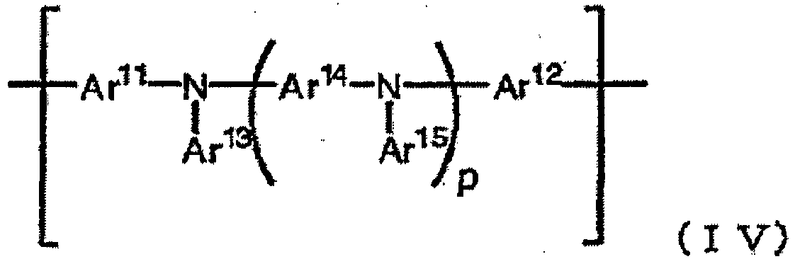 p représente un nombre entier de 0 à 3,Ar11 et Ar12 représentent chacun indépendamment une liaison directe ou un groupe cyclique aromatique qui peut avoir un substituant, etAr13 à Ar15 représentent chacun indépendamment un groupe cyclique aromatique qui peut avoir un substituant,Ar11 et Ar12 ne pouvant pas être à la fois une liaison directe.
 - Matériau de dispositif électronique, qui comprend le polymère selon la revendication 4 ou 5.
- Composition pour dispositif électronique, qui comprend le matériau de dispositif électronique selon la revendication 3 ou 6 et un solvant.
- Élément électroluminescent organique qui comprend une anode, une cathode et une couche organique intercalée entre l'anode et la cathode, dans lequel la couche organique comprend un composé qui est représenté par la formule générale (V) suivante et qui possède un poids moléculaire supérieur ou égal à 400 :
 R21 et R22 sont liés l'un à l'autre pour représenter un groupe représenté par -CH=CH- ou -CH2-CH2- ;Arb représente un groupe cyclique hydrocarboné aromatique qui peut avoir un substituant, dans lequel le substituant de Arb est sélectionné parmi les groupes cycliques hydrocarbonés aromatiques monovalents dérivés de monocycles ou de cycles condensés di- à penta-cycliques à 5 ou 6 chaînons ; les groupes hétérocycliques aromatiques monovalents dérivés de monocycles ou de cycles condensés di- à tétra-cycliques à 5 ou 6 chaînons ; et les groupes arylamino ayant un groupe cyclique hydrocarboné aromatique ayant 6 à 12 atomes de carbone, dans lequel les parties de chaîne hydrocarbonée dans le substituant de Arb possèdent 1 à 3 atomes de carbone ;d représente un nombre entier de 1 à 4 ou de 1 à 3 ; quand une pluralité de Arb est contenue dans la molécule, les Arb peuvent être identiques ou différents ; ou le polymère selon la revendication 4 ou 5 et dans lequel la couche organique est une couche formée par une méthode de formation de film humide au moyen de la composition pour dispositifs électroniques selon la revendication 7.
 - Élément électroluminescent organique selon la revendication 8, dans lequel la couche organique est une couche luminescente.
- Élément de cellules solaires organiques qui comprend une anode, une cathode et une couche organique intercalée entre l'anode et la cathode, dans lequel la couche organique comprend un composé qui est représenté par la formule générale (V) suivante et qui possède un poids moléculaire supérieur ou égal à 400 : dans laquelle
 R21 et R22 sont liés l'un à l'autre pour représenter un groupe représenté par -CH=CH- ou -CH2-CH2- ;Arb représente un groupe cyclique hydrocarboné aromatique qui peut avoir un substituant, dans lequel le substituant de Arb est sélectionné parmi les groupes cycliques hydrocarbonés aromatiques monovalents dérivés de monocycles ou de cycles condensés di- à penta-cycliques à 5 ou 6 chaînons ; les groupes hétérocycliques aromatiques monovalents dérivés de monocycles ou de cycles condensés di- à tétra-cycliques à 5 ou 6 chaînons ; et les groupes arylamino ayant un groupe cyclique hydrocarboné aromatique ayant 6 à 12 atomes de carbone, dans lequel les parties de chaîne hydrocarbonée dans le substituant de Arb possèdent 1 à 3 atomes de carbone ;d représente un nombre entier de 1 à 4 ou de 1 à 3 ; quand une pluralité de Arb est contenue dans la molécule, les Arb peuvent être identiques ou différents ; ou le polymère selon la revendication 4 ou 5 et dans lequel la couche organique est une couche formée par une méthode de formation de film humide au moyen de la composition pour dispositifs électroniques selon la revendication 7.
 - Affichage qui comprend l'élément électro-luminescent organique selon la revendication 8 ou 9.
- Éclairage qui comprend l'élément électro-luminescent organique selon la revendication 8 ou 9.
Applications Claiming Priority (2)
| Application Number | Priority Date | Filing Date | Title |
|---|---|---|---|
| JP2009251096 | 2009-10-30 | ||
| PCT/JP2010/069220 WO2011052698A1 (fr) | 2009-10-30 | 2010-10-28 | Composé de faible poids moléculaire, polymère, matériau pour dispositifs électroniques, composition pour dispositifs électroniques, élément organique électroluminescent, élément de cellule solaire organique, équipement d'affichage et d'éclairage |
Publications (3)
| Publication Number | Publication Date |
|---|---|
| EP2495229A1 EP2495229A1 (fr) | 2012-09-05 |
| EP2495229A4 EP2495229A4 (fr) | 2013-08-21 |
| EP2495229B1 true EP2495229B1 (fr) | 2016-06-01 |
Family
ID=43922121
Family Applications (1)
| Application Number | Title | Priority Date | Filing Date |
|---|---|---|---|
| EP10826830.1A Active EP2495229B1 (fr) | 2009-10-30 | 2010-10-28 | Composé de faible poids moléculaire, polymère, matériau pour dispositifs électroniques, composition pour dispositifs électroniques, élément organique électroluminescent, élément de cellule solaire organique, équipement d'affichage et d'éclairage |
Country Status (7)
| Country | Link |
|---|---|
| US (1) | US20120193617A1 (fr) |
| EP (1) | EP2495229B1 (fr) |
| JP (1) | JP5857743B2 (fr) |
| KR (1) | KR101830985B1 (fr) |
| CN (1) | CN102245543B (fr) |
| TW (1) | TWI485124B (fr) |
| WO (1) | WO2011052698A1 (fr) |
Families Citing this family (8)
| Publication number | Priority date | Publication date | Assignee | Title |
|---|---|---|---|---|
| EP2748877B1 (fr) * | 2011-08-26 | 2016-02-10 | Merck Patent GmbH | Formulation de semi-conducteurs organiques |
| KR20150052024A (ko) * | 2012-09-04 | 2015-05-13 | 미쯔비시 가가꾸 가부시끼가이샤 | 유기 전계 발광 소자 및 그의 제조 방법 |
| WO2017102048A1 (fr) * | 2015-12-15 | 2017-06-22 | Merck Patent Gmbh | Esters contenant des groupes aromatiques comme solvants pour formulations électroniques organiques |
| CN105576146B (zh) * | 2016-03-23 | 2017-09-26 | 京东方科技集团股份有限公司 | 发光器件及其制造方法和显示装置 |
| CN106920887A (zh) * | 2016-05-10 | 2017-07-04 | 广东聚华印刷显示技术有限公司 | 印刷oled器件及其制备方法 |
| US9831434B1 (en) | 2016-06-22 | 2017-11-28 | International Business Machines Corporation | Functionalized pyranopyran-derived acceptors for donor-acceptor polymers |
| CN106960922B (zh) * | 2017-04-10 | 2019-03-12 | 京东方科技集团股份有限公司 | 喷墨打印成膜方法 |
| EP3901194A4 (fr) * | 2018-12-20 | 2022-03-02 | Mitsubishi Chemical Corporation | Photodiode organique et capteur cmos infrarouge |
Family Cites Families (44)
| Publication number | Priority date | Publication date | Assignee | Title |
|---|---|---|---|---|
| US4539507A (en) | 1983-03-25 | 1985-09-03 | Eastman Kodak Company | Organic electroluminescent devices having improved power conversion efficiencies |
| US5061569A (en) | 1990-07-26 | 1991-10-29 | Eastman Kodak Company | Electroluminescent device with organic electroluminescent medium |
| JP3562652B2 (ja) | 1992-04-03 | 2004-09-08 | パイオニア株式会社 | 有機エレクトロルミネッセンス素子 |
| JPH06207169A (ja) | 1992-11-17 | 1994-07-26 | Idemitsu Kosan Co Ltd | 有機エレクトロルミネッセンス素子 |
| JP2734341B2 (ja) | 1993-03-26 | 1998-03-30 | 住友電気工業株式会社 | 有機エレクトロルミネッセンス素子 |
| JPH0753953A (ja) | 1993-08-19 | 1995-02-28 | Mitsubishi Chem Corp | 有機電界発光素子 |
| JPH1079297A (ja) | 1996-07-09 | 1998-03-24 | Sony Corp | 電界発光素子 |
| US5776622A (en) | 1996-07-29 | 1998-07-07 | Eastman Kodak Company | Bilayer eletron-injeting electrode for use in an electroluminescent device |
| US5645948A (en) | 1996-08-20 | 1997-07-08 | Eastman Kodak Company | Blue organic electroluminescent devices |
| JPH10270171A (ja) | 1997-01-27 | 1998-10-09 | Junji Kido | 有機エレクトロルミネッセント素子 |
| US6497969B2 (en) * | 1997-09-05 | 2002-12-24 | Nessdisplay Co., Ltd. | Electroluminescent device having an organic layer including polyimide |
| JPH11242996A (ja) | 1998-02-25 | 1999-09-07 | Mitsubishi Chemical Corp | 有機電界発光素子 |
| JPH11251067A (ja) | 1998-03-02 | 1999-09-17 | Junji Kido | 有機エレクトロルミネッセント素子 |
| JP4258583B2 (ja) * | 1999-02-23 | 2009-04-30 | 淳二 城戸 | 電界発光素子 |
| US6921588B2 (en) * | 1999-12-15 | 2005-07-26 | Samsung Sdi Co., Ltd. | Organic electroluminescent device having high luminance efficiency |
| JP2001223084A (ja) | 2000-02-07 | 2001-08-17 | Junji Kido | 有機電界発光素子 |
| JP2002100482A (ja) | 2000-09-20 | 2002-04-05 | Mitsubishi Chemicals Corp | 有機電界発光素子 |
| JP2002100478A (ja) | 2000-09-20 | 2002-04-05 | Mitsubishi Chemicals Corp | 有機電界発光素子及びその製造方法 |
| JP4023204B2 (ja) | 2001-05-02 | 2007-12-19 | 淳二 城戸 | 有機電界発光素子 |
| US7250226B2 (en) | 2001-08-31 | 2007-07-31 | Nippon Hoso Kyokai | Phosphorescent compound, a phosphorescent composition and an organic light-emitting device |
| JP3996036B2 (ja) | 2001-11-19 | 2007-10-24 | 三菱化学株式会社 | 芳香族ジアミン含有高分子化合物およびそれを用いる有機電界発光素子 |
| JP4502357B2 (ja) * | 2002-03-08 | 2010-07-14 | キヤノン株式会社 | 新規化合物とその合成方法、インク、インクカートリッジ、記録ユニット、インクジェット記録装置及び記録方法 |
| JP2004002740A (ja) | 2002-03-22 | 2004-01-08 | Mitsubishi Chemicals Corp | 高分子化合物、1,4−フェニレンジアミン誘導体、電荷輸送材料、有機電界発光素子材料および有機電界発光素子 |
| AU2003269913A1 (en) * | 2002-07-15 | 2004-02-02 | Massachusetts Institute Of Technology | Emissive, high charge transport polymers |
| EP1528074B1 (fr) * | 2002-08-09 | 2014-03-26 | Tosoh Corporation | Nouveau polymere triarylamine, son procede de production et son utilisation |
| US6969578B2 (en) * | 2002-08-19 | 2005-11-29 | Eastman Kodak Company | Optical recording material |
| US20060194073A1 (en) | 2003-03-07 | 2006-08-31 | Masato Okada | Organic compound and organic electrolumiscent device |
| GB0306409D0 (en) | 2003-03-20 | 2003-04-23 | Cambridge Display Tech Ltd | Electroluminescent device |
| JP2004362930A (ja) * | 2003-06-04 | 2004-12-24 | Mitsubishi Chemicals Corp | 有機電界発光素子、電荷輸送材料、及び有機電界発光素子材料 |
| JP2005022962A (ja) | 2003-06-11 | 2005-01-27 | Mitsubishi Materials Corp | ガラス組成物、混合体、ペースト、グリーンシートおよびpdp |
| JP4084271B2 (ja) | 2003-09-12 | 2008-04-30 | 株式会社リコー | 用紙後処理装置 |
| TW200530373A (en) * | 2003-12-12 | 2005-09-16 | Sumitomo Chemical Co | Polymer and light-emitting element using said polymer |
| JP2005243300A (ja) * | 2004-02-24 | 2005-09-08 | Sanyo Electric Co Ltd | 有機エレクトロルミネッセント素子及びその製造方法 |
| EP2325191A1 (fr) | 2004-03-11 | 2011-05-25 | Mitsubishi Chemical Corporation | Composition pour une couche transportant des charges et pour un composé ionique, couche transportant des charges et composant électroluminescent organique utilisant celle-ci |
| EP1728827A4 (fr) | 2004-03-25 | 2010-02-03 | Nissan Chemical Ind Ltd | Vernis a transport de charge et dispositifs electroluminescents organiques fabriques a l'aide dudit vernis |
| EP1768463A4 (fr) * | 2004-05-17 | 2011-04-13 | Zeon Corp | Élément électroluminescent, équipement d'éclairage et dispositif d'affichage |
| CN101014667A (zh) * | 2004-09-08 | 2007-08-08 | 佳能株式会社 | 颜料晶体制备阶段中的中间化学物质、使用它的颜料晶体制备方法、颜料晶体 |
| CN101115708B (zh) * | 2005-02-07 | 2010-10-13 | 出光兴产株式会社 | 芳香族胺衍生物以及使用其的有机电致发光元件 |
| GB2442656B (en) * | 2005-06-22 | 2009-12-23 | Sumitomo Chemical Co | Polymer material and polymer light-emitting device |
| US20090174326A1 (en) * | 2005-11-30 | 2009-07-09 | Sumitomo Chemical Company, Limited | Polymer material and polymer light-emitting device using same |
| JP5186757B2 (ja) * | 2006-11-27 | 2013-04-24 | コニカミノルタホールディングス株式会社 | 有機エレクトロルミネッセンス素子の製造方法、有機エレクトロルミネッセンス素子、表示装置及び照明装置 |
| US8187770B2 (en) * | 2007-10-19 | 2012-05-29 | The Regents Of The University Of California | High performance, crosslinked polymeric material for holographic data storage |
| EP2270069B1 (fr) * | 2008-02-15 | 2017-03-29 | Mitsubishi Chemical Corporation | Polymère conjugué, polymère insolubilisé, matière de dispositif électroluminescent organique, composition pour dispositif électroluminescent organique, procédé pour produire le polymère, dispositif électroluminescent organique, affichage el organique et illuminateur el organique |
| JP5075714B2 (ja) | 2008-04-02 | 2012-11-21 | 富士フイルム株式会社 | 色分解光学系および撮像装置 |
-
2010
- 2010-10-28 EP EP10826830.1A patent/EP2495229B1/fr active Active
- 2010-10-28 KR KR1020117012967A patent/KR101830985B1/ko active IP Right Grant
- 2010-10-28 JP JP2011538488A patent/JP5857743B2/ja active Active
- 2010-10-28 CN CN201080003531.6A patent/CN102245543B/zh active Active
- 2010-10-28 WO PCT/JP2010/069220 patent/WO2011052698A1/fr active Application Filing
- 2010-10-29 TW TW099137329A patent/TWI485124B/zh active
-
2012
- 2012-04-16 US US13/447,899 patent/US20120193617A1/en not_active Abandoned
Also Published As
| Publication number | Publication date |
|---|---|
| KR20120078666A (ko) | 2012-07-10 |
| US20120193617A1 (en) | 2012-08-02 |
| JPWO2011052698A1 (ja) | 2013-03-21 |
| CN102245543A (zh) | 2011-11-16 |
| KR101830985B1 (ko) | 2018-02-21 |
| EP2495229A1 (fr) | 2012-09-05 |
| WO2011052698A1 (fr) | 2011-05-05 |
| EP2495229A4 (fr) | 2013-08-21 |
| TW201124364A (en) | 2011-07-16 |
| TWI485124B (zh) | 2015-05-21 |
| JP5857743B2 (ja) | 2016-02-10 |
| CN102245543B (zh) | 2014-09-10 |
Similar Documents
| Publication | Publication Date | Title |
|---|---|---|
| JP5880654B2 (ja) | 発光層材料、有機電界発光素子用組成物、これらを利用した有機電界発光素子、有機el表示装置、及び有機el照明 | |
| EP2117062B1 (fr) | Composition pour un dispositif organique, membrane polymère et dispositif électroluminescent organique | |
| EP2314639B1 (fr) | Polymère transporteur de charges, composition pour élément électroluminescent organique, élément électroluminescent organique, dispositif d affichage électroluminescent organique et dispositif d éclairage électroluminescent organique | |
| KR101708064B1 (ko) | 유기 전계 발광 소자, 유기 el 표시 장치 및 유기 el 조명 | |
| EP3182479B1 (fr) | Polymère conjugué pour élément électroluminescent organique | |
| EP2695882B1 (fr) | Composé organique, matière de transport de charges, composition contenant ledit composé, élément électroluminescent organique, dispositif d'affichage et dispositif d'éclairage | |
| EP2495229B1 (fr) | Composé de faible poids moléculaire, polymère, matériau pour dispositifs électroniques, composition pour dispositifs électroniques, élément organique électroluminescent, élément de cellule solaire organique, équipement d'affichage et d'éclairage | |
| JP5434088B2 (ja) | 架橋性有機化合物、有機電界発光素子用組成物、有機電界発光素子および有機elディスプレイ | |
| EP2333862A1 (fr) | Procede de fabrication d'un element organique electroluminescent, element organique electroluminescent, affichage organique electroluminescent et eclairage organique electroluminescent | |
| KR20180128094A (ko) | 모노아민 화합물, 전하 수송 재료, 전하 수송막용 조성물, 유기 전계 발광 소자, 유기 el 표시 장치 및 유기 el 조명 | |
| JP5343818B2 (ja) | アリールアミンポリマー、有機電界発光素子材料、有機電界発光素子用組成物、有機電界発光素子、有機el表示装置及び有機el照明 | |
| JP4985441B2 (ja) | 高分子化合物、有機電界発光素子材料、有機電界発光素子用組成物および有機電界発光素子 | |
| JP5423064B2 (ja) | 有機電界発光素子用組成物、有機電界発光素子、有機elディスプレイ及び有機el照明 | |
| JP5685882B2 (ja) | 電荷輸送材料、電荷輸送膜用組成物、有機電界発光素子、有機電界発光素子表示装置及び有機電界発光素子照明装置 | |
| JP2010239134A (ja) | 有機電界発光素子、有機elディスプレイ及び有機el照明 | |
| JP2022136017A (ja) | 芳香族化合物 |
Legal Events
| Date | Code | Title | Description |
|---|---|---|---|
| PUAI | Public reference made under article 153(3) epc to a published international application that has entered the european phase |
Free format text: ORIGINAL CODE: 0009012 |
|
| 17P | Request for examination filed |
Effective date: 20110608 |
|
| AK | Designated contracting states |
Kind code of ref document: A1 Designated state(s): AL AT BE BG CH CY CZ DE DK EE ES FI FR GB GR HR HU IE IS IT LI LT LU LV MC MK MT NL NO PL PT RO RS SE SI SK SM TR |
|
| RIN1 | Information on inventor provided before grant (corrected) |
Inventor name: LI YANJUN Inventor name: URANO TOSHIYUKI Inventor name: NAKAI TOSHIMITSU Inventor name: IIDA KOICHIRO Inventor name: BABA TATSUSHI |
|
| DAX | Request for extension of the european patent (deleted) | ||
| A4 | Supplementary search report drawn up and despatched |
Effective date: 20130718 |
|
| RIC1 | Information provided on ipc code assigned before grant |
Ipc: C08G 73/02 20060101ALI20130712BHEP Ipc: C07C 211/45 20060101ALI20130712BHEP Ipc: C08G 61/12 20060101ALI20130712BHEP Ipc: H01L 51/50 20060101ALI20130712BHEP Ipc: H01L 51/42 20060101ALI20130712BHEP Ipc: C07C 13/605 20060101AFI20130712BHEP Ipc: C07C 13/44 20060101ALI20130712BHEP Ipc: C09K 11/06 20060101ALI20130712BHEP |
|
| 17Q | First examination report despatched |
Effective date: 20140214 |
|
| GRAP | Despatch of communication of intention to grant a patent |
Free format text: ORIGINAL CODE: EPIDOSNIGR1 |
|
| INTG | Intention to grant announced |
Effective date: 20150804 |
|
| GRAS | Grant fee paid |
Free format text: ORIGINAL CODE: EPIDOSNIGR3 |
|
| INTG | Intention to grant announced |
Effective date: 20160204 |
|
| GRAA | (expected) grant |
Free format text: ORIGINAL CODE: 0009210 |
|
| AK | Designated contracting states |
Kind code of ref document: B1 Designated state(s): AL AT BE BG CH CY CZ DE DK EE ES FI FR GB GR HR HU IE IS IT LI LT LU LV MC MK MT NL NO PL PT RO RS SE SI SK SM TR |
|
| REG | Reference to a national code |
Ref country code: GB Ref legal event code: FG4D |
|
| REG | Reference to a national code |
Ref country code: CH Ref legal event code: EP Ref country code: AT Ref legal event code: REF Ref document number: 803798 Country of ref document: AT Kind code of ref document: T Effective date: 20160615 |
|
| REG | Reference to a national code |
Ref country code: IE Ref legal event code: FG4D |
|
| REG | Reference to a national code |
Ref country code: DE Ref legal event code: R096 Ref document number: 602010033843 Country of ref document: DE |
|
| REG | Reference to a national code |
Ref country code: LT Ref legal event code: MG4D |
|
| REG | Reference to a national code |
Ref country code: NL Ref legal event code: MP Effective date: 20160601 |
|
| PG25 | Lapsed in a contracting state [announced via postgrant information from national office to epo] |
Ref country code: NO Free format text: LAPSE BECAUSE OF FAILURE TO SUBMIT A TRANSLATION OF THE DESCRIPTION OR TO PAY THE FEE WITHIN THE PRESCRIBED TIME-LIMIT Effective date: 20160901 Ref country code: LT Free format text: LAPSE BECAUSE OF FAILURE TO SUBMIT A TRANSLATION OF THE DESCRIPTION OR TO PAY THE FEE WITHIN THE PRESCRIBED TIME-LIMIT Effective date: 20160601 Ref country code: FI Free format text: LAPSE BECAUSE OF FAILURE TO SUBMIT A TRANSLATION OF THE DESCRIPTION OR TO PAY THE FEE WITHIN THE PRESCRIBED TIME-LIMIT Effective date: 20160601 |
|
| REG | Reference to a national code |
Ref country code: AT Ref legal event code: MK05 Ref document number: 803798 Country of ref document: AT Kind code of ref document: T Effective date: 20160601 |
|
| PG25 | Lapsed in a contracting state [announced via postgrant information from national office to epo] |
Ref country code: GR Free format text: LAPSE BECAUSE OF FAILURE TO SUBMIT A TRANSLATION OF THE DESCRIPTION OR TO PAY THE FEE WITHIN THE PRESCRIBED TIME-LIMIT Effective date: 20160902 Ref country code: HR Free format text: LAPSE BECAUSE OF FAILURE TO SUBMIT A TRANSLATION OF THE DESCRIPTION OR TO PAY THE FEE WITHIN THE PRESCRIBED TIME-LIMIT Effective date: 20160601 Ref country code: ES Free format text: LAPSE BECAUSE OF FAILURE TO SUBMIT A TRANSLATION OF THE DESCRIPTION OR TO PAY THE FEE WITHIN THE PRESCRIBED TIME-LIMIT Effective date: 20160601 Ref country code: RS Free format text: LAPSE BECAUSE OF FAILURE TO SUBMIT A TRANSLATION OF THE DESCRIPTION OR TO PAY THE FEE WITHIN THE PRESCRIBED TIME-LIMIT Effective date: 20160601 Ref country code: SE Free format text: LAPSE BECAUSE OF FAILURE TO SUBMIT A TRANSLATION OF THE DESCRIPTION OR TO PAY THE FEE WITHIN THE PRESCRIBED TIME-LIMIT Effective date: 20160601 Ref country code: LV Free format text: LAPSE BECAUSE OF FAILURE TO SUBMIT A TRANSLATION OF THE DESCRIPTION OR TO PAY THE FEE WITHIN THE PRESCRIBED TIME-LIMIT Effective date: 20160601 Ref country code: NL Free format text: LAPSE BECAUSE OF FAILURE TO SUBMIT A TRANSLATION OF THE DESCRIPTION OR TO PAY THE FEE WITHIN THE PRESCRIBED TIME-LIMIT Effective date: 20160601 |
|
| PG25 | Lapsed in a contracting state [announced via postgrant information from national office to epo] |
Ref country code: SK Free format text: LAPSE BECAUSE OF FAILURE TO SUBMIT A TRANSLATION OF THE DESCRIPTION OR TO PAY THE FEE WITHIN THE PRESCRIBED TIME-LIMIT Effective date: 20160601 Ref country code: IS Free format text: LAPSE BECAUSE OF FAILURE TO SUBMIT A TRANSLATION OF THE DESCRIPTION OR TO PAY THE FEE WITHIN THE PRESCRIBED TIME-LIMIT Effective date: 20161001 Ref country code: CZ Free format text: LAPSE BECAUSE OF FAILURE TO SUBMIT A TRANSLATION OF THE DESCRIPTION OR TO PAY THE FEE WITHIN THE PRESCRIBED TIME-LIMIT Effective date: 20160601 Ref country code: RO Free format text: LAPSE BECAUSE OF FAILURE TO SUBMIT A TRANSLATION OF THE DESCRIPTION OR TO PAY THE FEE WITHIN THE PRESCRIBED TIME-LIMIT Effective date: 20160601 Ref country code: IT Free format text: LAPSE BECAUSE OF FAILURE TO SUBMIT A TRANSLATION OF THE DESCRIPTION OR TO PAY THE FEE WITHIN THE PRESCRIBED TIME-LIMIT Effective date: 20160601 Ref country code: EE Free format text: LAPSE BECAUSE OF FAILURE TO SUBMIT A TRANSLATION OF THE DESCRIPTION OR TO PAY THE FEE WITHIN THE PRESCRIBED TIME-LIMIT Effective date: 20160601 |
|
| PG25 | Lapsed in a contracting state [announced via postgrant information from national office to epo] |
Ref country code: SM Free format text: LAPSE BECAUSE OF FAILURE TO SUBMIT A TRANSLATION OF THE DESCRIPTION OR TO PAY THE FEE WITHIN THE PRESCRIBED TIME-LIMIT Effective date: 20160601 Ref country code: AT Free format text: LAPSE BECAUSE OF FAILURE TO SUBMIT A TRANSLATION OF THE DESCRIPTION OR TO PAY THE FEE WITHIN THE PRESCRIBED TIME-LIMIT Effective date: 20160601 Ref country code: PL Free format text: LAPSE BECAUSE OF FAILURE TO SUBMIT A TRANSLATION OF THE DESCRIPTION OR TO PAY THE FEE WITHIN THE PRESCRIBED TIME-LIMIT Effective date: 20160601 Ref country code: BE Free format text: LAPSE BECAUSE OF NON-PAYMENT OF DUE FEES Effective date: 20160601 Ref country code: PT Free format text: LAPSE BECAUSE OF FAILURE TO SUBMIT A TRANSLATION OF THE DESCRIPTION OR TO PAY THE FEE WITHIN THE PRESCRIBED TIME-LIMIT Effective date: 20161003 |
|
| REG | Reference to a national code |
Ref country code: DE Ref legal event code: R097 Ref document number: 602010033843 Country of ref document: DE |
|
| PLBE | No opposition filed within time limit |
Free format text: ORIGINAL CODE: 0009261 |
|
| STAA | Information on the status of an ep patent application or granted ep patent |
Free format text: STATUS: NO OPPOSITION FILED WITHIN TIME LIMIT |
|
| 26N | No opposition filed |
Effective date: 20170302 |
|
| PG25 | Lapsed in a contracting state [announced via postgrant information from national office to epo] |
Ref country code: DK Free format text: LAPSE BECAUSE OF FAILURE TO SUBMIT A TRANSLATION OF THE DESCRIPTION OR TO PAY THE FEE WITHIN THE PRESCRIBED TIME-LIMIT Effective date: 20160601 Ref country code: SI Free format text: LAPSE BECAUSE OF FAILURE TO SUBMIT A TRANSLATION OF THE DESCRIPTION OR TO PAY THE FEE WITHIN THE PRESCRIBED TIME-LIMIT Effective date: 20160601 |
|
| REG | Reference to a national code |
Ref country code: CH Ref legal event code: PL |
|
| GBPC | Gb: european patent ceased through non-payment of renewal fee |
Effective date: 20161028 |
|
| REG | Reference to a national code |
Ref country code: IE Ref legal event code: MM4A |
|
| REG | Reference to a national code |
Ref country code: FR Ref legal event code: ST Effective date: 20170630 |
|
| PG25 | Lapsed in a contracting state [announced via postgrant information from national office to epo] |
Ref country code: GB Free format text: LAPSE BECAUSE OF NON-PAYMENT OF DUE FEES Effective date: 20161028 Ref country code: CH Free format text: LAPSE BECAUSE OF NON-PAYMENT OF DUE FEES Effective date: 20161031 Ref country code: LI Free format text: LAPSE BECAUSE OF NON-PAYMENT OF DUE FEES Effective date: 20161031 Ref country code: FR Free format text: LAPSE BECAUSE OF NON-PAYMENT OF DUE FEES Effective date: 20161102 |
|
| PG25 | Lapsed in a contracting state [announced via postgrant information from national office to epo] |
Ref country code: LU Free format text: LAPSE BECAUSE OF NON-PAYMENT OF DUE FEES Effective date: 20161028 |
|
| REG | Reference to a national code |
Ref country code: DE Ref legal event code: R082 Ref document number: 602010033843 Country of ref document: DE Representative=s name: VOSSIUS & PARTNER PATENTANWAELTE RECHTSANWAELT, DE Ref country code: DE Ref legal event code: R081 Ref document number: 602010033843 Country of ref document: DE Owner name: MITSUBISHI CHEMICAL CORPORATION, JP Free format text: FORMER OWNER: MITSUBISHI CHEMICAL CORPORATION, TOKIO, JP |
|
| PG25 | Lapsed in a contracting state [announced via postgrant information from national office to epo] |
Ref country code: IE Free format text: LAPSE BECAUSE OF NON-PAYMENT OF DUE FEES Effective date: 20161028 |
|
| PG25 | Lapsed in a contracting state [announced via postgrant information from national office to epo] |
Ref country code: HU Free format text: LAPSE BECAUSE OF FAILURE TO SUBMIT A TRANSLATION OF THE DESCRIPTION OR TO PAY THE FEE WITHIN THE PRESCRIBED TIME-LIMIT; INVALID AB INITIO Effective date: 20101028 Ref country code: CY Free format text: LAPSE BECAUSE OF FAILURE TO SUBMIT A TRANSLATION OF THE DESCRIPTION OR TO PAY THE FEE WITHIN THE PRESCRIBED TIME-LIMIT Effective date: 20160601 |
|
| PG25 | Lapsed in a contracting state [announced via postgrant information from national office to epo] |
Ref country code: MK Free format text: LAPSE BECAUSE OF FAILURE TO SUBMIT A TRANSLATION OF THE DESCRIPTION OR TO PAY THE FEE WITHIN THE PRESCRIBED TIME-LIMIT Effective date: 20160601 Ref country code: MT Free format text: LAPSE BECAUSE OF NON-PAYMENT OF DUE FEES Effective date: 20161031 Ref country code: TR Free format text: LAPSE BECAUSE OF FAILURE TO SUBMIT A TRANSLATION OF THE DESCRIPTION OR TO PAY THE FEE WITHIN THE PRESCRIBED TIME-LIMIT Effective date: 20160601 Ref country code: MC Free format text: LAPSE BECAUSE OF FAILURE TO SUBMIT A TRANSLATION OF THE DESCRIPTION OR TO PAY THE FEE WITHIN THE PRESCRIBED TIME-LIMIT Effective date: 20160601 |
|
| PG25 | Lapsed in a contracting state [announced via postgrant information from national office to epo] |
Ref country code: BG Free format text: LAPSE BECAUSE OF FAILURE TO SUBMIT A TRANSLATION OF THE DESCRIPTION OR TO PAY THE FEE WITHIN THE PRESCRIBED TIME-LIMIT Effective date: 20160601 |
|
| PG25 | Lapsed in a contracting state [announced via postgrant information from national office to epo] |
Ref country code: AL Free format text: LAPSE BECAUSE OF FAILURE TO SUBMIT A TRANSLATION OF THE DESCRIPTION OR TO PAY THE FEE WITHIN THE PRESCRIBED TIME-LIMIT Effective date: 20160601 |
|
| P01 | Opt-out of the competence of the unified patent court (upc) registered |
Effective date: 20230522 |
|
| PGFP | Annual fee paid to national office [announced via postgrant information from national office to epo] |
Ref country code: DE Payment date: 20230906 Year of fee payment: 14 |