EP2487796A2 - Ausgangskreis, System mit dem Ausgangskreis und Verfahren zur Steuerung des Ausgangskreises - Google Patents
Ausgangskreis, System mit dem Ausgangskreis und Verfahren zur Steuerung des Ausgangskreises Download PDFInfo
- Publication number
- EP2487796A2 EP2487796A2 EP20120151757 EP12151757A EP2487796A2 EP 2487796 A2 EP2487796 A2 EP 2487796A2 EP 20120151757 EP20120151757 EP 20120151757 EP 12151757 A EP12151757 A EP 12151757A EP 2487796 A2 EP2487796 A2 EP 2487796A2
- Authority
- EP
- European Patent Office
- Prior art keywords
- transistor
- circuit
- coupled
- output circuit
- terminal
- Prior art date
- Legal status (The legal status is an assumption and is not a legal conclusion. Google has not performed a legal analysis and makes no representation as to the accuracy of the status listed.)
- Granted
Links
Images


Classifications
-
- H—ELECTRICITY
- H03—ELECTRONIC CIRCUITRY
- H03K—PULSE TECHNIQUE
- H03K19/00—Logic circuits, i.e. having at least two inputs acting on one output; Inverting circuits
- H03K19/0175—Coupling arrangements; Interface arrangements
- H03K19/0185—Coupling arrangements; Interface arrangements using field effect transistors only
- H03K19/018507—Interface arrangements
-
- H—ELECTRICITY
- H03—ELECTRONIC CIRCUITRY
- H03K—PULSE TECHNIQUE
- H03K19/00—Logic circuits, i.e. having at least two inputs acting on one output; Inverting circuits
- H03K19/003—Modifications for increasing the reliability for protection
- H03K19/00346—Modifications for eliminating interference or parasitic voltages or currents
- H03K19/00361—Modifications for eliminating interference or parasitic voltages or currents in field effect transistor circuits
Definitions
- the present application relates to an output circuit, a system including the output circuit, and a method of controlling the output circuit.
- Communication among a plurality of devices is, for example, conventionally carried out by serial communication.
- Such devices include an open-drain type output circuit (see Japanese Patent Publication No. 2009-531934 ).
- a plurality of devices 11, 12, and 13 is mutually coupled by a transmission path 14 which transmits and receives data.
- the device 13 includes an output circuit 15 which outputs data.
- other devices 11 and 12 also include a similar output circuit.
- the output circuit 15 is an open drain type driver circuit.
- a resistor R1 pulls up a potential level of the transmission path 14.
- the device 13 activates an N-channel MOS transistor T1, which is coupled to an external terminal P0, to pull down the potential level of the transmission path 14, which is coupled to the external terminal P0.
- the voltage Vc of the signal propagated through the transmission path 14 is changed, as illustrated in Fig. 2A .
- the output circuit 15 activates the N-channel MOS transistor T1 to change the potential of the transmission path 14 from H level to L level.
- a waveform shaping capacitor C1 may be coupled between a gate and a drain of the transistor T1 to adjust the slope of the fall edge of the potential level in the transmission path 14.
- the power supply of the device 13 that does not perform the communication may be turned off.
- the supply of high potential voltage VDE to an inverter circuit 16, for example is stopped.
- a gate terminal of the transistor T1 is in a floating state.
- the gate terminal of the transistor T1 of the output circuit 15 is AC coupled with the transmission path 14 through the waveform shaping capacitor C1. Therefore, when the potential of the transmission path 14 changes from L level to H level, the gate voltage of the transistor T1 also rises.
- the transistor T1 is then weakly activated. As a result, the waveform of the voltage Vc in the transmission path 14 changes, as illustrated in Fig. 2B . That is, the signal waveform propagated through the transmission path 14 changes undesirably.
- an output circuit includes a first transistor coupled to an external terminal and including a gate terminal that receives a first drive signal.
- the first transistor drives a potential at the external terminal in accordance with the first drive signal.
- a first capacitor includes a first end coupled to the gate terminal of the first transistor and a second end coupled to the external terminal.
- the output circuit also includes a circuit portion coupled to the first transistor. The circuit portion maintains the first transistor in an inactivated state when the gate terminal of the first transistor is in a floating state. According to this embodiment, the signal waveform is suppressed from undesirably changing.
- a system includes a plurality of devices that communicate with each other through a transmission path coupled to an external terminal.
- Each of the plurality of devices includes an output circuit.
- the output circuit includes a first transistor coupled to an external terminal and including a gate terminal that receives a first drive signal.
- the first transistor drives a potential at the external terminal in accordance with the first drive signal.
- a first capacitor includes a first end coupled to the gate terminal of the first transistor and a second end coupled to the external terminal.
- a circuit portion coupled to the first transistor maintains the first transistor in an inactivated state when the gate terminal of the first transistor is in a floating state. According to this embodiment, the signal waveform is suppressed from undesirably changing.
- a method of controlling an output circuit including a first transistor, a first capacitor, and a second transistor, the first transistor coupled to an external terminal and including a gate terminal that receives a first drive signal, the first capacitor including a first end coupled to the gate terminal of the first transistor and a second end coupled to the external terminal, and the second transistor coupled to the first transistor, the method including: driving the first transistor with the first drive signal; and maintaining the first transistor in an inactivated state by the second transistor when the gate terminal of the first transistor is in a floating state.
- the signal waveform is suppressed from undesirably changing.
- Fig. 1 is a schematic circuit block diagram of a system including an output circuit
- Figs. 2A and 2B are waveform charts illustrating change in potential level of a transmission path between devices
- Fig. 3 is a schematic circuit block diagram of a system including an output circuit
- Fig. 4 is a schematic block diagram of a device
- Fig. 5 is a schematic circuit diagram of an input/output circuit of a first embodiment
- Fig. 6 is a schematic operation waveform chart of the input/output circuit of Fig. 5 ;
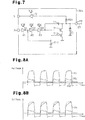
- Fig. 7 is a schematic circuit diagram of an input/output circuit of a second embodiment
- Fig. 8A is a schematic operation waveform chart of the input/output circuit of Fig. 7 ;
- Fig. 8B is a schematic operation waveform chart of the input/output circuit, where a solid line indicates the operation waveform of the input/output circuit of Fig. 1 , and a dashed line indicates the waveform of the gate voltage of the transistor T1 of the input/output circuit of Fig. 5 .
- an electronic system includes a plurality of (four in Fig. 3 ) of devices 21, 22, 23, and 24.
- the devices 21 to 24 are coupled to each other by a bus 25.
- the devices 21 to 24 are formed to transmit and receive signals and data with each other through the bus 25 in accordance with a given synchronous serial communication.
- the synchronous serial communication is, for example, an Inter Integrated Circuit communication.
- the bus 25 includes, for example, a first transmission path 26, which transmits a clock signal, and a second transmission path 27, which transmits data.
- each of the transmission paths 26 and 27 is a cable or a pattern wiring formed on a substrate.
- a resistor R11 is arranged on the first transmission path 26.
- the resistor R11 includes a first terminal coupled to the first transmission path 26 and a second terminal supplied with a voltage Vp.
- the resistor R11 pulls up a potential level in the first transmission path 26.
- a resistor R12 is arranged on the second transmission path 27.
- the resistor R12 includes a first terminal coupled to the second transmission path 27 and a second terminal supplied with the voltage Vp.
- the resistor R12 pulls up a potential level in the second transmission path 27.
- At least one of the devices 21 to 24 is formed to operate as a master device.
- the master device is a microcontroller that generates a clock signal for data transfer and outputs the clock signal to the first transmission path 26.
- the master device starts and terminates the data transfer on the bus.
- the device whose address is instructed by the master device is called a slave device.
- the device 21 is the master device, and the devices 22 to 24 are the slave devices.
- the device 22 includes a logic circuit 31 that operates by a first high potential voltage VDI.
- the logic circuit 31 is coupled to an input/output circuit 33 that operates by a second high potential voltage VDE through a shift circuit 32.
- the shift circuit 32 shifts a level of the signal, which is output from the logic circuit 31, to a level of the signal, which is handled by the input/output circuits 33 and 34. Further, the shift circuit 32 shifts a level of the signal, which is output from the input/output circuits 33 and 34, to a level of the signal, which is handled by the logic circuit 31.
- the logic circuit 31 includes, for example, a CPU, or the like, and has a data processing function and a communication control function.
- the input/output circuit 33 pulls down a potential level in the transmission path 26 coupled to an external terminal P1 based on a signal provided from the logic circuit 31 through the shift circuit 32.
- the input/output circuit 33 outputs a signal based on the change in the potential level of the transmission path 26 to the shift circuit 32.
- the input/output circuit 34 pulls down a potential level in the transmission path 27 coupled to an external terminal P2 based on a signal provided from the logic circuit 31 through the shift circuit 32.
- the input/output circuit 34 outputs a signal based on the change in the potential level of the transmission path 27 to the shift circuit 32.
- the input/output circuit 34 includes inverter circuits 41 to 43.
- a signal So is provided to the inverter circuit 41 based on a signal output from the shift circuit 32 illustrated in Fig. 4 .
- An output terminal of the inverter circuit 41 is coupled to an input terminal of the inverter circuit 42.
- An output terminal of the inverter circuit 42 is coupled to an input terminal of the inverter circuit 43.
- the inverter circuits 41 to 43 coupled in series in this manner operate by the high potential voltage VDE supplied as a drive voltage.
- An output terminal of the inverter circuit 43 is coupled to a pull-down transistor T1.
- the transistor T1 is an N-channel MOS transistor and includes a gate terminal coupled to the output terminal of the inverter circuit 43, a source terminal coupled to the wiring supplied with a low potential voltage (reference potential, e.g., ground potential), and a drain terminal coupled to the external terminal P2.
- the wiring supplied with the low potential voltage is the ground.
- a waveform shaping capacitor C1 is coupled to the transistor T1.
- the capacitor C1 includes a first terminal coupled to the drain terminal of the transistor T1 and a second terminal coupled to the gate terminal of the transistor T1.
- the capacitor C1 has a capacitance value that is set such that the slope of the fall (Fall-rate) of the potential level of the transmission path 27 conforms to the provision of the communication.
- the external terminal P2 is coupled to a cathode of a diode D1.
- An anode of the diode D1 is coupled to the ground.
- the diode D1 is arranged as a protective element from en electrostatic discharge (ESD).
- a first terminal of the capacitor C2 is coupled to the external terminal P2.
- a second terminal of the capacitor C2 is coupled to the transistor T2.
- the capacitor C2 has a capacitance value that is set to, for example, about 1/10 of the capacitance value of the capacitor C1.
- the transistor T2 has the same conductivity type as the pull-down transistor T1.
- the transistor T2 is an N-channel MOS transistor.
- the transistor T2 includes a gate terminal coupled to the second terminal of the capacitor C2, a source terminal coupled to the ground, and a drain terminal coupled to the gate terminal of the transistor T1 (i.e., second terminal of capacitor C1).
- the gate terminal of the transistor T2 is coupled to a transistor T3.
- the transistor T3 has the same conductivity type as the transistors T1 and T2.
- the transistor T3 is an N-channel MOS transistor.
- the transistor T3 includes a drain terminal coupled to the gate terminal of the transistor T2, a source terminal coupled to the ground, and a gate terminal supplied with the high potential voltage VDE.
- a first terminal of the resistor R21 is coupled to the external terminal P2.
- a second terminal of the resistor R21 is coupled to an input terminal of a buffer circuit 51.
- the buffer circuit 51 is, for example, a Schmidt trigger gate.
- the buffer circuit 51 operates by the high potential voltage VDE supplied as a drive voltage.
- An output signal Si of the buffer circuit 51 is provided to the logic circuit 31 through the shift circuit 32 illustrated in Fig. 4 .
- Fig. 5 illustrates the input/output circuit 34 for driving the transmission path 27, the input/output circuit 33 for driving the transmission path 26 illustrated in Fig. 4 is also similarly formed.
- the transistor T3 When the power supply (high potential voltage VDE) is supplied to the input/output circuit 34 of the device 22, the transistor T3 is activated by the high potential voltage VDE to set the gate voltage of the transistor T2 to ground level. Thus, the transistor T2 is inactivated.
- the inverter circuit 43 When the signal So is H level, the inverter circuit 43 provides the signal S3 of L level to the gate terminal of the transistor T1. The transistor T1 is inactivated in response to the signal S3 of L level. In this case, the potential level of the transmission path 27 is pulled up by the resistor R12 illustrated in Fig. 3 . That is, the potential of the transmission path 27 becomes H level.
- the inverter circuit 43 raises the gate voltage of the transistor T1 from L level.
- the inverter circuit 43 is formed by a high potential side transistor, which is coupled to the wiring supplied with the high potential voltage, and a low potential side transistor, which is coupled to the ground.
- the inverter circuit 43 further includes a resistor element (not illustrated) coupled between the output terminal of the inverter circuit 43 and the high potential side transistor.
- the resistor element of the inverter circuit 43 gradually raises the gate voltage of the transistor T1. That is, the current supplied to the gate terminal of the transistor T1 is set by the resistor element.
- the transistor T1 is activated when the gate voltage of the transistor T1 reaches the threshold voltage of the transistor T1.
- the drain current of the transistor T1 gradually increases according to the rise in the gate voltage of the transistor T1. This gradually pulls down the potential level of the transmission path 27.
- the transistor T3 When the power supply (high potential voltage VDE) is not supplied to the input/output circuit 34 of the device 22, the transistor T3 is inactivated and the gate terminal of the transistor T2 is in a floating state.
- the potential level of the transmission path 27 is pulled down by the operation of another device (e.g., device 23 illustrated in Fig. 3 ) and set to L level.
- another device e.g., device 23 illustrated in Fig. 3
- the pull down transistor (T1) of another device is inactivated, the potential level of the transmission path 27 is pulled up by the resistor R12 (see Fig. 3 ) and raised from L level to H level.
- the gate terminal of the transistor T1 illustrated in Fig. 5 is AC coupled with the external terminal P2 through the capacitor C1. Therefore, the gate voltage of the transistor T1 rises according to the rise in the potential level of the transmission path 27.
- the gate terminal of the transistor T2 is also AC coupled with the external terminal P2 through the capacitor C2. Therefore, the gate voltage of the transistor T2 rises according to the rise in the potential level of the transmission path 27.
- the parasitic capacitance of the transistor T2 is sufficiently small compared to the parasitic capacitance of the gate of the transistor T1.
- the capacitance value of the capacitor C2 may be set smaller than the capacitance value of the capacitor C1.
- the capacitance value of the capacitor C2 is set to about 1/10 of the capacitance value of the capacitor C1, as described above.
- the gate voltage of the transistor T2 rises faster than the gate voltage of the transistor T1.
- the transistor T2 is activated before the transistor T1.
- the transistor T2 that is activated couples the gate terminal of the transistor T1 to the wiring supplied with the low potential voltage (ground potential).
- the transistor T2 and the capacitor C2 are included in a pull-down circuit 44 that pulls down the potential at the gate terminal of the transistor T1.
- the pull-down circuit 44 is an example of a circuit portion that maintains the transistor T1 in an inactivated state when the gate terminal of the transistor T1 is in the floating state.
- the transistor T2 that is activated by the terminal voltage of the capacitor C2 couples the second terminal of the capacitor C1, which is coupled to the gate terminal of the transistor T1, to the ground.
- the charges of the capacitor C1 which are charged by the rise in the potential level of the transmission path 27 flow toward the ground, thus pulling down the gate voltage of the transistor T1 to the ground level. Therefore, the transistor T1 maintains the inactivated state.
- the voltage Vc of the transmission path 27 changes from L level to H level by the operation of the input/output circuit of another device.
- the transistor T1 of the input/output circuit 34 is not activated in an unintended manner and the voltage Vc of the transmission path 27 does not lower to the undesired level even if the power supply of the device 22 is turned off.
- the waveform illustrated by a dashed line in Fig. 6 indicates the change in waveform obtained by the circuit structure illustrated in Fig. 1 .
- the output circuit of the first embodiment has the following advantages.
- the first transistor T1 is activated and inactivated in response to the signal S3.
- the transistor T1 that is activated pulls down the potential level in the transmission path 27 coupled to the external terminal P2.
- the potential level of the transmission path 27 falls at the slope corresponding to the capacitance value of the capacitor C1, which AC couples the gate terminal of the transistor T1 and the external terminal P2.
- the pull-down circuit 44 pulls down the gate voltage of the transistor T1 in accordance with the potential at the external terminal P2 and inactivates the transistor T1.
- the rising waveform of the potential level in the transmission path 27 coupled to the external terminal P2 is suppressed from undesirably changing.
- the transistor T3 is coupled to the gate terminal of the transistor T2.
- the high potential voltage VDE is supplied to the gate terminal of the transistor T3.
- the transistor T3 is activated, thereby pulling down the gate voltage of the transistor T2. Therefore, when the high potential voltage VDE is supplied, the transistor T2 is inactivated and the signal S3 activates and inactivates the transistor T1.
- an input/output circuit 34a includes two transistors T11 and T12 that are cascade coupled, or series coupled.
- the first transistor T11 and the second transistor T12 are the same conductivity type as the transistor T1 illustrated in Fig. 5 , that is, the N-channel MOS transistors.
- the drain terminal of the first transistor T11 is coupled to the external terminal P2.
- the source terminal of the first transistor T11 is coupled to the drain terminal of the second transistor T12.
- the source terminal of the second transistor T12 is coupled to the wiring supplied with the low potential voltage (reference potential, e.g., ground potential).
- the wiring supplied with the low potential voltage is the ground in the present embodiment.
- the first transistor T11 and the second transistor T12 are formed to pull down the potential level of the transmission path 27, similar to the transistor T1 illustrated in Fig. 3 .
- the gate width of each of transistors T11 and T12 is set to be twice the gate width of the transistor T1 ( Fig. 5 ) so that the current substantially equal to the switching current flowing from the external terminal P2 towards the ground when the transistor T1 ( Fig. 5 ) is activated flows to the transistors T11 and T12.
- the gate terminal of the first transistor T11 is coupled to the output terminal of the inverter circuit 43.
- the waveform shaping capacitor C1 is coupled between the gate terminal and the drain terminal of the first transistor T11.
- the gate terminal of the second transistor T12 is coupled to the output terminal of the inverter circuit 41.
- the gate terminal of the second transistor T12 is also coupled to a first terminal of the capacitor C11.
- a second terminal of the capacitor C11 is coupled to the ground.
- the inverter circuit 43 is an example of a first gate circuit
- the inverter circuit 41 is an example of a second gate circuit
- the signal S3 is an example of a first drive signal
- the signal S1 is an example of a second drive signal.
- the second transistor T12 and the capacitor C11 form a circuit portion that maintains the first transistor T11 in an inactivated state when the gate terminal of the first transistor T11 is in the floating state.
- Fig. 7 illustrates the input/output circuit 34a for driving the transmission path 27, the input/output circuit 33 for driving the transmission path 26 illustrated in Fig. 4 is also similarly formed.
- the output signal S1 of the inverter circuit 41 responding to the signal So is provided to the gate terminal of the second transistor T12. Further, the output signal S1 of the inverter circuit 41 is provided to the gate terminal of the first transistor T11 as the signal S3 through the two inverter circuits 42 and 43. Therefore, the signal substantially in phase with respect to each other is provided to the gate terminal of the first transistor T11 and the gate terminal of the second transistor T12. That is, the first transistor T11 and the second transistor T12 are activated and inactivated substantially in phase. In other words, the signal S1 and the signal S3 involve a substantially similar logical change. The first and second transistors T11 and T12 that are activated pull down the potential level of the transmission path 27.
- the gate terminal of the first transistor T11 is in the floating state.
- the gate voltage VG1 of the first transistor T11 fluctuates, as illustrated by a dashed line in Fig. 8A , due to the AC coupling of the waveform shaping capacitor C1.
- the dashed line illustrated in Fig. 8B indicates the waveform of the gate voltage of the transistor T1 illustrated in Fig. 5 .
- the gate voltage VG2 of the second transistor T12 is AC coupled to the ground via the capacitor C11.
- the gate voltage VG2 of the second transistor T12 is held at a stable potential (around ground level).
- the gate voltage VG2 does not exceed the threshold voltage of the second transistor T12. Therefore, the second transistor T12 continues the inactivated state.
- the output circuit of the second embodiment has the following advantages.
- the first transistor T11 and the second transistor T12 are coupled in series between the external terminal P2 and the ground.
- the first transistor T11 is activated and inactivated in response to the signal S3 output from the inverter circuit 43.
- the second transistor T12 is activated and inactivated in response to the signal S1 output from the inverter circuit 41.
- the waveform shaping capacitor C1 is coupled between the gate terminal of the first transistor T11 and the external terminal P2.
- the gate terminal of the second transistor T12 is coupled to the ground via the capacitor C11.
- the capacitor C11 holds the gate voltage of the transistor T12 at around the ground level. As a result, the transistor T12 is inactivated. Thus, even if the potential level in the transmission path 27 coupled to the external terminal P2 changes by the operation of another device and the gate voltage of the first transistor T11 fluctuates by the AC coupling of the capacitor C1, the second transistor T12 continues the inactivated state. This suppresses the first transistor T11 from being activated in an unintended manner. In other words, the waveform of the voltage Vc of the transmission path 27 is suppressed from undesirably changing.
- the output circuit may be formed by combining the structure illustrated in Fig. 5 (transistors T2 and T3 and capacitor C2) and the structure illustrated in Fig. 7 (transistor T12 and capacitor C11).
- the input/output circuit 34a illustrated in Fig. 5 may further include the transistor T12 and the capacitor C11 illustrated in Fig. 7 .
- the input/output circuit 34 may be formed as an output circuit omitting the function of the input circuit (resistor R21 and buffer circuit 51) from the circuit 34 (or 34a).
- the transistors that form the input/output circuit 34 are not limited to the MOS transistors, and may be bipolar transistors.
- the first high potential voltage VDI and the second high potential voltage VDE are illustrated as in Fig. 4 .
- the structure of the output circuit (input/output circuit) described above may be applied to the device in which a single voltage is supplied to the logic circuit 31 and the input/output circuit 33.
Landscapes
- Engineering & Computer Science (AREA)
- Computer Hardware Design (AREA)
- Physics & Mathematics (AREA)
- Computing Systems (AREA)
- General Engineering & Computer Science (AREA)
- Mathematical Physics (AREA)
- Logic Circuits (AREA)
- Electronic Switches (AREA)
Applications Claiming Priority (1)
| Application Number | Priority Date | Filing Date | Title |
|---|---|---|---|
| JP2011028880A JP5516449B2 (ja) | 2011-02-14 | 2011-02-14 | 出力回路、システム、及び出力回路の制御方法 |
Publications (3)
| Publication Number | Publication Date |
|---|---|
| EP2487796A2 true EP2487796A2 (de) | 2012-08-15 |
| EP2487796A3 EP2487796A3 (de) | 2013-07-31 |
| EP2487796B1 EP2487796B1 (de) | 2018-01-03 |
Family
ID=45531218
Family Applications (1)
| Application Number | Title | Priority Date | Filing Date |
|---|---|---|---|
| EP12151757.7A Not-in-force EP2487796B1 (de) | 2011-02-14 | 2012-01-19 | Ausgangskreis, System mit dem Ausgangskreis und Verfahren zur Steuerung des Ausgangskreises |
Country Status (4)
| Country | Link |
|---|---|
| US (1) | US8487649B2 (de) |
| EP (1) | EP2487796B1 (de) |
| JP (1) | JP5516449B2 (de) |
| CN (1) | CN102638258B (de) |
Families Citing this family (4)
| Publication number | Priority date | Publication date | Assignee | Title |
|---|---|---|---|---|
| US10854586B1 (en) * | 2019-05-24 | 2020-12-01 | Bae Systems Information And Electronics Systems Integration Inc. | Multi-chip module hybrid integrated circuit with multiple power zones that provide cold spare support |
| US10990471B2 (en) | 2019-05-29 | 2021-04-27 | Bae Systems Information And Electronic Systems Integration Inc. | Apparatus and method for reducing radiation induced multiple-bit memory soft errors |
| US11342915B1 (en) | 2021-02-11 | 2022-05-24 | Bae Systems Information And Electronic Systems Integration Inc. | Cold spare tolerant radiation hardened generic level shifter circuit |
| JP2023147535A (ja) * | 2022-03-30 | 2023-10-13 | ラピステクノロジー株式会社 | 信号入出力回路 |
Citations (1)
| Publication number | Priority date | Publication date | Assignee | Title |
|---|---|---|---|---|
| JP2009531934A (ja) | 2006-03-31 | 2009-09-03 | エヌエックスピー ビー ヴィ | 容量帰還を用いる信号ドライバのための方法およびシステム |
Family Cites Families (11)
| Publication number | Priority date | Publication date | Assignee | Title |
|---|---|---|---|---|
| US5051625B1 (en) * | 1988-10-28 | 1993-11-16 | Nissan Motor Co.,Ltd. | Output buffer circuits for reducing noise |
| US5334889A (en) * | 1990-06-20 | 1994-08-02 | Oki Electric Industry, Co., Ltd. | CMOS output buffer circuit with less noise |
| US5117129A (en) | 1990-10-16 | 1992-05-26 | International Business Machines Corporation | Cmos off chip driver for fault tolerant cold sparing |
| FR2813461B1 (fr) | 2000-08-22 | 2003-01-31 | St Microelectronics Sa | Dispositif de protection d'un transistor integre contre des decharges electrostatiques |
| JP3844120B2 (ja) | 2001-10-19 | 2006-11-08 | 株式会社ルネサステクノロジ | 半導体装置 |
| US20040017698A1 (en) * | 2002-07-25 | 2004-01-29 | Micron Technology, Inc. | Refined gate coupled noise compensation for open-drain output from semiconductor device |
| JP4817372B2 (ja) * | 2006-03-28 | 2011-11-16 | 富士通セミコンダクター株式会社 | オープンドレイン出力回路 |
| JP4973243B2 (ja) * | 2007-03-06 | 2012-07-11 | 富士通セミコンダクター株式会社 | 半導体出力回路及び外部出力信号生成方法並びに半導体装置 |
| US7852110B2 (en) * | 2008-05-21 | 2010-12-14 | Texas Instruments Incorporated | Controlling the slew-rate of an output buffer |
| US8072721B2 (en) | 2009-06-10 | 2011-12-06 | Hong Kong Applied Science And Technology Research Institute Co., Ltd. | ESD protection using a capacitivly-coupled clamp for protecting low-voltage core transistors from high-voltage outputs |
| JP5565336B2 (ja) * | 2011-02-14 | 2014-08-06 | 富士通セミコンダクター株式会社 | 出力回路、システム、及び出力回路の制御方法 |
-
2011
- 2011-02-14 JP JP2011028880A patent/JP5516449B2/ja active Active
-
2012
- 2012-01-17 CN CN201210024935.4A patent/CN102638258B/zh active Active
- 2012-01-17 US US13/351,797 patent/US8487649B2/en active Active
- 2012-01-19 EP EP12151757.7A patent/EP2487796B1/de not_active Not-in-force
Patent Citations (1)
| Publication number | Priority date | Publication date | Assignee | Title |
|---|---|---|---|---|
| JP2009531934A (ja) | 2006-03-31 | 2009-09-03 | エヌエックスピー ビー ヴィ | 容量帰還を用いる信号ドライバのための方法およびシステム |
Also Published As
| Publication number | Publication date |
|---|---|
| JP2012169843A (ja) | 2012-09-06 |
| US20120206186A1 (en) | 2012-08-16 |
| JP5516449B2 (ja) | 2014-06-11 |
| EP2487796B1 (de) | 2018-01-03 |
| CN102638258A (zh) | 2012-08-15 |
| CN102638258B (zh) | 2014-12-03 |
| EP2487796A3 (de) | 2013-07-31 |
| US8487649B2 (en) | 2013-07-16 |
Similar Documents
| Publication | Publication Date | Title |
|---|---|---|
| US9257973B1 (en) | Supply-state-enabled level shifter interface circuit and method | |
| EP2624455B1 (de) | Pegelschieberschaltung | |
| US7859314B2 (en) | Method and system for a signal driver using capacitive feedback | |
| EP1102402A1 (de) | Pegelregelungsschaltung und Datenausgangsschaltung | |
| CN108804368B (zh) | 能够连接到串行外围接口总线的缓冲器级设备 | |
| CN106257668A (zh) | 半导体器件 | |
| US9385718B1 (en) | Input-output buffer circuit with a gate bias generator | |
| EP2487796A2 (de) | Ausgangskreis, System mit dem Ausgangskreis und Verfahren zur Steuerung des Ausgangskreises | |
| US7999569B2 (en) | Edge rate suppression for open drain buses | |
| US8614598B2 (en) | Output circuit, system including output circuit, and method of controlling output circuit | |
| EP1999849B1 (de) | Elektronische vorrichtung und integrierte schaltung | |
| CN118300573A (zh) | 一种驱动电路、lin总线以及驱动方法 | |
| JP2002204154A (ja) | 終端回路およびその方法 | |
| US7663407B2 (en) | Semiconductor device having transfer gate between pre-buffer and main buffer | |
| CN114095004A (zh) | 驱动电路 | |
| CN103578525B (zh) | 用于限流地给节点再充电的电路 | |
| US20160241233A1 (en) | Driver circuit for single wire protocol slave unit | |
| JP5689778B2 (ja) | 入力回路 | |
| JP6113489B2 (ja) | 半導体回路及び半導体装置 | |
| CN114817112A (zh) | 一种从机设备以及主从机通信系统 | |
| JP5509187B2 (ja) | 出力バッファ回路およびファンアウトバッファ |
Legal Events
| Date | Code | Title | Description |
|---|---|---|---|
| PUAI | Public reference made under article 153(3) epc to a published international application that has entered the european phase |
Free format text: ORIGINAL CODE: 0009012 |
|
| AK | Designated contracting states |
Kind code of ref document: A2 Designated state(s): AL AT BE BG CH CY CZ DE DK EE ES FI FR GB GR HR HU IE IS IT LI LT LU LV MC MK MT NL NO PL PT RO RS SE SI SK SM TR |
|
| AX | Request for extension of the european patent |
Extension state: BA ME |
|
| RIC1 | Information provided on ipc code assigned before grant |
Ipc: H03K 19/003 20060101AFI20130319BHEP Ipc: H03K 19/0185 20060101ALI20130319BHEP |
|
| PUAL | Search report despatched |
Free format text: ORIGINAL CODE: 0009013 |
|
| AK | Designated contracting states |
Kind code of ref document: A3 Designated state(s): AL AT BE BG CH CY CZ DE DK EE ES FI FR GB GR HR HU IE IS IT LI LT LU LV MC MK MT NL NO PL PT RO RS SE SI SK SM TR |
|
| AX | Request for extension of the european patent |
Extension state: BA ME |
|
| RIC1 | Information provided on ipc code assigned before grant |
Ipc: H03K 19/0185 20060101ALI20130625BHEP Ipc: H03K 19/003 20060101AFI20130625BHEP |
|
| 17P | Request for examination filed |
Effective date: 20140127 |
|
| RBV | Designated contracting states (corrected) |
Designated state(s): AL AT BE BG CH CY CZ DE DK EE ES FI FR GB GR HR HU IE IS IT LI LT LU LV MC MK MT NL NO PL PT RO RS SE SI SK SM TR |
|
| 17Q | First examination report despatched |
Effective date: 20140226 |
|
| RAP1 | Party data changed (applicant data changed or rights of an application transferred) |
Owner name: SOCIONEXT INC. |
|
| GRAP | Despatch of communication of intention to grant a patent |
Free format text: ORIGINAL CODE: EPIDOSNIGR1 |
|
| INTG | Intention to grant announced |
Effective date: 20170727 |
|
| GRAS | Grant fee paid |
Free format text: ORIGINAL CODE: EPIDOSNIGR3 |
|
| GRAA | (expected) grant |
Free format text: ORIGINAL CODE: 0009210 |
|
| AK | Designated contracting states |
Kind code of ref document: B1 Designated state(s): AL AT BE BG CH CY CZ DE DK EE ES FI FR GB GR HR HU IE IS IT LI LT LU LV MC MK MT NL NO PL PT RO RS SE SI SK SM TR |
|
| REG | Reference to a national code |
Ref country code: GB Ref legal event code: FG4D |
|
| REG | Reference to a national code |
Ref country code: CH Ref legal event code: EP Ref country code: AT Ref legal event code: REF Ref document number: 961150 Country of ref document: AT Kind code of ref document: T Effective date: 20180115 |
|
| REG | Reference to a national code |
Ref country code: IE Ref legal event code: FG4D |
|
| REG | Reference to a national code |
Ref country code: DE Ref legal event code: R096 Ref document number: 602012041518 Country of ref document: DE |
|
| REG | Reference to a national code |
Ref country code: NL Ref legal event code: MP Effective date: 20180103 |
|
| REG | Reference to a national code |
Ref country code: LT Ref legal event code: MG4D |
|
| REG | Reference to a national code |
Ref country code: AT Ref legal event code: MK05 Ref document number: 961150 Country of ref document: AT Kind code of ref document: T Effective date: 20180103 |
|
| PG25 | Lapsed in a contracting state [announced via postgrant information from national office to epo] |
Ref country code: NL Free format text: LAPSE BECAUSE OF FAILURE TO SUBMIT A TRANSLATION OF THE DESCRIPTION OR TO PAY THE FEE WITHIN THE PRESCRIBED TIME-LIMIT Effective date: 20180103 |
|
| PG25 | Lapsed in a contracting state [announced via postgrant information from national office to epo] |
Ref country code: LT Free format text: LAPSE BECAUSE OF FAILURE TO SUBMIT A TRANSLATION OF THE DESCRIPTION OR TO PAY THE FEE WITHIN THE PRESCRIBED TIME-LIMIT Effective date: 20180103 Ref country code: CY Free format text: LAPSE BECAUSE OF FAILURE TO SUBMIT A TRANSLATION OF THE DESCRIPTION OR TO PAY THE FEE WITHIN THE PRESCRIBED TIME-LIMIT Effective date: 20180103 Ref country code: FI Free format text: LAPSE BECAUSE OF FAILURE TO SUBMIT A TRANSLATION OF THE DESCRIPTION OR TO PAY THE FEE WITHIN THE PRESCRIBED TIME-LIMIT Effective date: 20180103 Ref country code: ES Free format text: LAPSE BECAUSE OF FAILURE TO SUBMIT A TRANSLATION OF THE DESCRIPTION OR TO PAY THE FEE WITHIN THE PRESCRIBED TIME-LIMIT Effective date: 20180103 Ref country code: NO Free format text: LAPSE BECAUSE OF FAILURE TO SUBMIT A TRANSLATION OF THE DESCRIPTION OR TO PAY THE FEE WITHIN THE PRESCRIBED TIME-LIMIT Effective date: 20180403 Ref country code: HR Free format text: LAPSE BECAUSE OF FAILURE TO SUBMIT A TRANSLATION OF THE DESCRIPTION OR TO PAY THE FEE WITHIN THE PRESCRIBED TIME-LIMIT Effective date: 20180103 |
|
| PG25 | Lapsed in a contracting state [announced via postgrant information from national office to epo] |
Ref country code: RS Free format text: LAPSE BECAUSE OF FAILURE TO SUBMIT A TRANSLATION OF THE DESCRIPTION OR TO PAY THE FEE WITHIN THE PRESCRIBED TIME-LIMIT Effective date: 20180103 Ref country code: SE Free format text: LAPSE BECAUSE OF FAILURE TO SUBMIT A TRANSLATION OF THE DESCRIPTION OR TO PAY THE FEE WITHIN THE PRESCRIBED TIME-LIMIT Effective date: 20180103 Ref country code: LV Free format text: LAPSE BECAUSE OF FAILURE TO SUBMIT A TRANSLATION OF THE DESCRIPTION OR TO PAY THE FEE WITHIN THE PRESCRIBED TIME-LIMIT Effective date: 20180103 Ref country code: BG Free format text: LAPSE BECAUSE OF FAILURE TO SUBMIT A TRANSLATION OF THE DESCRIPTION OR TO PAY THE FEE WITHIN THE PRESCRIBED TIME-LIMIT Effective date: 20180403 Ref country code: AT Free format text: LAPSE BECAUSE OF FAILURE TO SUBMIT A TRANSLATION OF THE DESCRIPTION OR TO PAY THE FEE WITHIN THE PRESCRIBED TIME-LIMIT Effective date: 20180103 Ref country code: IS Free format text: LAPSE BECAUSE OF FAILURE TO SUBMIT A TRANSLATION OF THE DESCRIPTION OR TO PAY THE FEE WITHIN THE PRESCRIBED TIME-LIMIT Effective date: 20180503 Ref country code: GR Free format text: LAPSE BECAUSE OF FAILURE TO SUBMIT A TRANSLATION OF THE DESCRIPTION OR TO PAY THE FEE WITHIN THE PRESCRIBED TIME-LIMIT Effective date: 20180404 Ref country code: PL Free format text: LAPSE BECAUSE OF FAILURE TO SUBMIT A TRANSLATION OF THE DESCRIPTION OR TO PAY THE FEE WITHIN THE PRESCRIBED TIME-LIMIT Effective date: 20180103 |
|
| REG | Reference to a national code |
Ref country code: CH Ref legal event code: PL |
|
| REG | Reference to a national code |
Ref country code: DE Ref legal event code: R097 Ref document number: 602012041518 Country of ref document: DE |
|
| PG25 | Lapsed in a contracting state [announced via postgrant information from national office to epo] |
Ref country code: MC Free format text: LAPSE BECAUSE OF FAILURE TO SUBMIT A TRANSLATION OF THE DESCRIPTION OR TO PAY THE FEE WITHIN THE PRESCRIBED TIME-LIMIT Effective date: 20180103 Ref country code: AL Free format text: LAPSE BECAUSE OF FAILURE TO SUBMIT A TRANSLATION OF THE DESCRIPTION OR TO PAY THE FEE WITHIN THE PRESCRIBED TIME-LIMIT Effective date: 20180103 Ref country code: LU Free format text: LAPSE BECAUSE OF NON-PAYMENT OF DUE FEES Effective date: 20180119 Ref country code: RO Free format text: LAPSE BECAUSE OF FAILURE TO SUBMIT A TRANSLATION OF THE DESCRIPTION OR TO PAY THE FEE WITHIN THE PRESCRIBED TIME-LIMIT Effective date: 20180103 Ref country code: IT Free format text: LAPSE BECAUSE OF FAILURE TO SUBMIT A TRANSLATION OF THE DESCRIPTION OR TO PAY THE FEE WITHIN THE PRESCRIBED TIME-LIMIT Effective date: 20180103 Ref country code: EE Free format text: LAPSE BECAUSE OF FAILURE TO SUBMIT A TRANSLATION OF THE DESCRIPTION OR TO PAY THE FEE WITHIN THE PRESCRIBED TIME-LIMIT Effective date: 20180103 |
|
| REG | Reference to a national code |
Ref country code: IE Ref legal event code: MM4A |
|
| REG | Reference to a national code |
Ref country code: BE Ref legal event code: MM Effective date: 20180131 |
|
| PLBE | No opposition filed within time limit |
Free format text: ORIGINAL CODE: 0009261 |
|
| STAA | Information on the status of an ep patent application or granted ep patent |
Free format text: STATUS: NO OPPOSITION FILED WITHIN TIME LIMIT |
|
| PG25 | Lapsed in a contracting state [announced via postgrant information from national office to epo] |
Ref country code: SK Free format text: LAPSE BECAUSE OF FAILURE TO SUBMIT A TRANSLATION OF THE DESCRIPTION OR TO PAY THE FEE WITHIN THE PRESCRIBED TIME-LIMIT Effective date: 20180103 Ref country code: LI Free format text: LAPSE BECAUSE OF NON-PAYMENT OF DUE FEES Effective date: 20180131 Ref country code: SM Free format text: LAPSE BECAUSE OF FAILURE TO SUBMIT A TRANSLATION OF THE DESCRIPTION OR TO PAY THE FEE WITHIN THE PRESCRIBED TIME-LIMIT Effective date: 20180103 Ref country code: CH Free format text: LAPSE BECAUSE OF NON-PAYMENT OF DUE FEES Effective date: 20180131 Ref country code: DK Free format text: LAPSE BECAUSE OF FAILURE TO SUBMIT A TRANSLATION OF THE DESCRIPTION OR TO PAY THE FEE WITHIN THE PRESCRIBED TIME-LIMIT Effective date: 20180103 Ref country code: BE Free format text: LAPSE BECAUSE OF NON-PAYMENT OF DUE FEES Effective date: 20180131 Ref country code: CZ Free format text: LAPSE BECAUSE OF FAILURE TO SUBMIT A TRANSLATION OF THE DESCRIPTION OR TO PAY THE FEE WITHIN THE PRESCRIBED TIME-LIMIT Effective date: 20180103 |
|
| 26N | No opposition filed |
Effective date: 20181005 |
|
| GBPC | Gb: european patent ceased through non-payment of renewal fee |
Effective date: 20180403 |
|
| PG25 | Lapsed in a contracting state [announced via postgrant information from national office to epo] |
Ref country code: IE Free format text: LAPSE BECAUSE OF NON-PAYMENT OF DUE FEES Effective date: 20180119 |
|
| PG25 | Lapsed in a contracting state [announced via postgrant information from national office to epo] |
Ref country code: SI Free format text: LAPSE BECAUSE OF FAILURE TO SUBMIT A TRANSLATION OF THE DESCRIPTION OR TO PAY THE FEE WITHIN THE PRESCRIBED TIME-LIMIT Effective date: 20180103 Ref country code: GB Free format text: LAPSE BECAUSE OF NON-PAYMENT OF DUE FEES Effective date: 20180403 |
|
| PG25 | Lapsed in a contracting state [announced via postgrant information from national office to epo] |
Ref country code: FR Free format text: LAPSE BECAUSE OF NON-PAYMENT OF DUE FEES Effective date: 20180303 |
|
| PG25 | Lapsed in a contracting state [announced via postgrant information from national office to epo] |
Ref country code: MT Free format text: LAPSE BECAUSE OF NON-PAYMENT OF DUE FEES Effective date: 20180119 |
|
| PG25 | Lapsed in a contracting state [announced via postgrant information from national office to epo] |
Ref country code: TR Free format text: LAPSE BECAUSE OF FAILURE TO SUBMIT A TRANSLATION OF THE DESCRIPTION OR TO PAY THE FEE WITHIN THE PRESCRIBED TIME-LIMIT Effective date: 20180103 |
|
| PG25 | Lapsed in a contracting state [announced via postgrant information from national office to epo] |
Ref country code: HU Free format text: LAPSE BECAUSE OF FAILURE TO SUBMIT A TRANSLATION OF THE DESCRIPTION OR TO PAY THE FEE WITHIN THE PRESCRIBED TIME-LIMIT; INVALID AB INITIO Effective date: 20120119 Ref country code: PT Free format text: LAPSE BECAUSE OF FAILURE TO SUBMIT A TRANSLATION OF THE DESCRIPTION OR TO PAY THE FEE WITHIN THE PRESCRIBED TIME-LIMIT Effective date: 20180103 |
|
| PG25 | Lapsed in a contracting state [announced via postgrant information from national office to epo] |
Ref country code: MK Free format text: LAPSE BECAUSE OF NON-PAYMENT OF DUE FEES Effective date: 20180103 |
|
| REG | Reference to a national code |
Ref country code: DE Ref legal event code: R082 Ref document number: 602012041518 Country of ref document: DE Representative=s name: HL KEMPNER PATENTANWALT, RECHTSANWALT, SOLICIT, DE |
|
| PGFP | Annual fee paid to national office [announced via postgrant information from national office to epo] |
Ref country code: DE Payment date: 20220119 Year of fee payment: 11 |
|
| REG | Reference to a national code |
Ref country code: DE Ref legal event code: R119 Ref document number: 602012041518 Country of ref document: DE |
|
| PG25 | Lapsed in a contracting state [announced via postgrant information from national office to epo] |
Ref country code: DE Free format text: LAPSE BECAUSE OF NON-PAYMENT OF DUE FEES Effective date: 20230801 |