EP2470954B1 - Procede de fabrication des vitrages electrochromes - Google Patents
Procede de fabrication des vitrages electrochromes Download PDFInfo
- Publication number
- EP2470954B1 EP2470954B1 EP10757863.5A EP10757863A EP2470954B1 EP 2470954 B1 EP2470954 B1 EP 2470954B1 EP 10757863 A EP10757863 A EP 10757863A EP 2470954 B1 EP2470954 B1 EP 2470954B1
- Authority
- EP
- European Patent Office
- Prior art keywords
- layers
- glass
- electrochromic
- layer
- substrates
- Prior art date
- Legal status (The legal status is an assumption and is not a legal conclusion. Google has not performed a legal analysis and makes no representation as to the accuracy of the status listed.)
- Active
Links
- 238000004519 manufacturing process Methods 0.000 title claims description 43
- 239000000758 substrate Substances 0.000 claims description 96
- 239000011521 glass Substances 0.000 claims description 78
- 238000000034 method Methods 0.000 claims description 59
- 238000000576 coating method Methods 0.000 claims description 32
- 239000010416 ion conductor Substances 0.000 claims description 23
- 238000000059 patterning Methods 0.000 claims description 9
- QGLKJKCYBOYXKC-UHFFFAOYSA-N nonaoxidotritungsten Chemical compound O=[W]1(=O)O[W](=O)(=O)O[W](=O)(=O)O1 QGLKJKCYBOYXKC-UHFFFAOYSA-N 0.000 claims description 8
- 238000004544 sputter deposition Methods 0.000 claims description 8
- 229910001930 tungsten oxide Inorganic materials 0.000 claims description 8
- BQCADISMDOOEFD-UHFFFAOYSA-N Silver Chemical compound [Ag] BQCADISMDOOEFD-UHFFFAOYSA-N 0.000 claims description 7
- 229910052709 silver Inorganic materials 0.000 claims description 6
- 239000004332 silver Substances 0.000 claims description 5
- 230000000903 blocking effect Effects 0.000 claims description 3
- VNNRSPGTAMTISX-UHFFFAOYSA-N chromium nickel Chemical compound [Cr].[Ni] VNNRSPGTAMTISX-UHFFFAOYSA-N 0.000 claims description 2
- 238000010884 ion-beam technique Methods 0.000 claims description 2
- 229910001120 nichrome Inorganic materials 0.000 claims description 2
- 229920000642 polymer Polymers 0.000 claims description 2
- 229910012305 LiPON Inorganic materials 0.000 claims 1
- 238000005520 cutting process Methods 0.000 claims 1
- 238000010030 laminating Methods 0.000 claims 1
- 239000010410 layer Substances 0.000 description 120
- 230000008569 process Effects 0.000 description 31
- 238000000151 deposition Methods 0.000 description 29
- 239000000463 material Substances 0.000 description 27
- 230000008021 deposition Effects 0.000 description 26
- 239000010408 film Substances 0.000 description 21
- 239000011248 coating agent Substances 0.000 description 20
- 239000002200 LIPON - lithium phosphorus oxynitride Substances 0.000 description 18
- 229910052744 lithium Inorganic materials 0.000 description 13
- 230000004888 barrier function Effects 0.000 description 12
- 239000003792 electrolyte Substances 0.000 description 12
- WHXSMMKQMYFTQS-UHFFFAOYSA-N Lithium Chemical compound [Li] WHXSMMKQMYFTQS-UHFFFAOYSA-N 0.000 description 11
- 230000008901 benefit Effects 0.000 description 10
- 230000005540 biological transmission Effects 0.000 description 10
- XEEYBQQBJWHFJM-UHFFFAOYSA-N iron Substances [Fe] XEEYBQQBJWHFJM-UHFFFAOYSA-N 0.000 description 10
- 238000004513 sizing Methods 0.000 description 10
- 238000004040 coloring Methods 0.000 description 9
- 230000010354 integration Effects 0.000 description 9
- 150000002500 ions Chemical class 0.000 description 9
- 230000002829 reductive effect Effects 0.000 description 9
- 238000005496 tempering Methods 0.000 description 9
- 230000007547 defect Effects 0.000 description 8
- 238000010586 diagram Methods 0.000 description 8
- 238000001704 evaporation Methods 0.000 description 8
- 238000010348 incorporation Methods 0.000 description 8
- 238000013461 design Methods 0.000 description 7
- 230000008020 evaporation Effects 0.000 description 7
- 230000007935 neutral effect Effects 0.000 description 7
- 230000003287 optical effect Effects 0.000 description 7
- 239000010409 thin film Substances 0.000 description 7
- 239000005341 toughened glass Substances 0.000 description 7
- 238000010521 absorption reaction Methods 0.000 description 6
- 230000008859 change Effects 0.000 description 6
- 238000005516 engineering process Methods 0.000 description 6
- 238000003475 lamination Methods 0.000 description 6
- 239000003570 air Substances 0.000 description 5
- 238000011161 development Methods 0.000 description 5
- 238000003780 insertion Methods 0.000 description 5
- 229910015867 LixMyOz Inorganic materials 0.000 description 4
- 238000013459 approach Methods 0.000 description 4
- 230000001351 cycling effect Effects 0.000 description 4
- 230000000694 effects Effects 0.000 description 4
- 230000006872 improvement Effects 0.000 description 4
- 230000037431 insertion Effects 0.000 description 4
- 238000012545 processing Methods 0.000 description 4
- 230000009467 reduction Effects 0.000 description 4
- 238000001878 scanning electron micrograph Methods 0.000 description 4
- 238000002834 transmittance Methods 0.000 description 4
- 238000000429 assembly Methods 0.000 description 3
- 230000015572 biosynthetic process Effects 0.000 description 3
- 230000015556 catabolic process Effects 0.000 description 3
- 238000001816 cooling Methods 0.000 description 3
- 238000006731 degradation reaction Methods 0.000 description 3
- 238000005137 deposition process Methods 0.000 description 3
- 230000004313 glare Effects 0.000 description 3
- 238000010438 heat treatment Methods 0.000 description 3
- 238000009830 intercalation Methods 0.000 description 3
- 239000011229 interlayer Substances 0.000 description 3
- 229910052742 iron Inorganic materials 0.000 description 3
- 238000002955 isolation Methods 0.000 description 3
- 229910001416 lithium ion Inorganic materials 0.000 description 3
- 230000002441 reversible effect Effects 0.000 description 3
- 238000012546 transfer Methods 0.000 description 3
- IJGRMHOSHXDMSA-UHFFFAOYSA-N Atomic nitrogen Chemical compound N#N IJGRMHOSHXDMSA-UHFFFAOYSA-N 0.000 description 2
- 229910013292 LiNiO Inorganic materials 0.000 description 2
- 229910016226 LixNi1-xO Inorganic materials 0.000 description 2
- 229910014279 LixNi1−xO Inorganic materials 0.000 description 2
- 229910005855 NiOx Inorganic materials 0.000 description 2
- 229910052581 Si3N4 Inorganic materials 0.000 description 2
- 229910003070 TaOx Inorganic materials 0.000 description 2
- 230000003667 anti-reflective effect Effects 0.000 description 2
- 230000000712 assembly Effects 0.000 description 2
- QVGXLLKOCUKJST-UHFFFAOYSA-N atomic oxygen Chemical compound [O] QVGXLLKOCUKJST-UHFFFAOYSA-N 0.000 description 2
- 238000006243 chemical reaction Methods 0.000 description 2
- 239000003086 colorant Substances 0.000 description 2
- 239000002131 composite material Substances 0.000 description 2
- 239000004020 conductor Substances 0.000 description 2
- 230000008878 coupling Effects 0.000 description 2
- 238000010168 coupling process Methods 0.000 description 2
- 238000005859 coupling reaction Methods 0.000 description 2
- 238000009792 diffusion process Methods 0.000 description 2
- 239000012777 electrically insulating material Substances 0.000 description 2
- 239000007772 electrode material Substances 0.000 description 2
- 239000002001 electrolyte material Substances 0.000 description 2
- 230000008030 elimination Effects 0.000 description 2
- 238000003379 elimination reaction Methods 0.000 description 2
- 238000005265 energy consumption Methods 0.000 description 2
- 238000011066 ex-situ storage Methods 0.000 description 2
- 239000005357 flat glass Substances 0.000 description 2
- 229920000592 inorganic polymer Polymers 0.000 description 2
- 230000003993 interaction Effects 0.000 description 2
- 230000002687 intercalation Effects 0.000 description 2
- URIIGZKXFBNRAU-UHFFFAOYSA-N lithium;oxonickel Chemical compound [Li].[Ni]=O URIIGZKXFBNRAU-UHFFFAOYSA-N 0.000 description 2
- 230000007774 longterm Effects 0.000 description 2
- 230000007246 mechanism Effects 0.000 description 2
- 229910052751 metal Inorganic materials 0.000 description 2
- 239000002184 metal Substances 0.000 description 2
- 150000004706 metal oxides Chemical group 0.000 description 2
- 239000000203 mixture Substances 0.000 description 2
- 230000004048 modification Effects 0.000 description 2
- 238000012986 modification Methods 0.000 description 2
- 238000005457 optimization Methods 0.000 description 2
- 229920000620 organic polymer Polymers 0.000 description 2
- 229910052760 oxygen Inorganic materials 0.000 description 2
- 239000001301 oxygen Substances 0.000 description 2
- 230000005855 radiation Effects 0.000 description 2
- 238000001552 radio frequency sputter deposition Methods 0.000 description 2
- 238000005478 sputtering type Methods 0.000 description 2
- 230000003068 static effect Effects 0.000 description 2
- 229910052720 vanadium Inorganic materials 0.000 description 2
- OKTJSMMVPCPJKN-UHFFFAOYSA-N Carbon Chemical compound [C] OKTJSMMVPCPJKN-UHFFFAOYSA-N 0.000 description 1
- 238000012369 In process control Methods 0.000 description 1
- 229910013928 LiCo0.95Mg0.05O2 Inorganic materials 0.000 description 1
- 229910032387 LiCoO2 Inorganic materials 0.000 description 1
- 229910014235 MyOz Inorganic materials 0.000 description 1
- 230000006750 UV protection Effects 0.000 description 1
- 238000002835 absorbance Methods 0.000 description 1
- 239000000654 additive Substances 0.000 description 1
- 229910052782 aluminium Inorganic materials 0.000 description 1
- 239000012080 ambient air Substances 0.000 description 1
- 238000000137 annealing Methods 0.000 description 1
- 239000010405 anode material Substances 0.000 description 1
- 230000009286 beneficial effect Effects 0.000 description 1
- 239000007844 bleaching agent Substances 0.000 description 1
- 229910052799 carbon Inorganic materials 0.000 description 1
- 239000000919 ceramic Substances 0.000 description 1
- 230000000295 complement effect Effects 0.000 description 1
- 238000012864 cross contamination Methods 0.000 description 1
- 230000003247 decreasing effect Effects 0.000 description 1
- 230000001934 delay Effects 0.000 description 1
- 230000006866 deterioration Effects 0.000 description 1
- 230000001627 detrimental effect Effects 0.000 description 1
- 230000006353 environmental stress Effects 0.000 description 1
- 238000000605 extraction Methods 0.000 description 1
- 230000002349 favourable effect Effects 0.000 description 1
- 238000009501 film coating Methods 0.000 description 1
- 239000011888 foil Substances 0.000 description 1
- 238000009472 formulation Methods 0.000 description 1
- 150000004820 halides Chemical class 0.000 description 1
- BHEPBYXIRTUNPN-UHFFFAOYSA-N hydridophosphorus(.) (triplet) Chemical compound [PH] BHEPBYXIRTUNPN-UHFFFAOYSA-N 0.000 description 1
- 229910052739 hydrogen Inorganic materials 0.000 description 1
- 238000010965 in-process control Methods 0.000 description 1
- 238000011065 in-situ storage Methods 0.000 description 1
- 229910010272 inorganic material Inorganic materials 0.000 description 1
- 239000011147 inorganic material Substances 0.000 description 1
- 230000002427 irreversible effect Effects 0.000 description 1
- 238000010329 laser etching Methods 0.000 description 1
- 238000006138 lithiation reaction Methods 0.000 description 1
- 229910001386 lithium phosphate Inorganic materials 0.000 description 1
- 229910052749 magnesium Inorganic materials 0.000 description 1
- 229910044991 metal oxide Inorganic materials 0.000 description 1
- 150000002739 metals Chemical class 0.000 description 1
- 229910052750 molybdenum Inorganic materials 0.000 description 1
- 238000012544 monitoring process Methods 0.000 description 1
- 229910000480 nickel oxide Inorganic materials 0.000 description 1
- 229910052758 niobium Inorganic materials 0.000 description 1
- 229910052757 nitrogen Inorganic materials 0.000 description 1
- 239000011368 organic material Substances 0.000 description 1
- 239000007800 oxidant agent Substances 0.000 description 1
- GNRSAWUEBMWBQH-UHFFFAOYSA-N oxonickel Chemical compound [Ni]=O GNRSAWUEBMWBQH-UHFFFAOYSA-N 0.000 description 1
- 238000002294 plasma sputter deposition Methods 0.000 description 1
- XOFYZVNMUHMLCC-ZPOLXVRWSA-N prednisone Chemical compound O=C1C=C[C@]2(C)[C@H]3C(=O)C[C@](C)([C@@](CC4)(O)C(=O)CO)[C@@H]4[C@@H]3CCC2=C1 XOFYZVNMUHMLCC-ZPOLXVRWSA-N 0.000 description 1
- 238000004886 process control Methods 0.000 description 1
- 238000013341 scale-up Methods 0.000 description 1
- 238000012216 screening Methods 0.000 description 1
- 238000000926 separation method Methods 0.000 description 1
- 229910052710 silicon Inorganic materials 0.000 description 1
- HQVNEWCFYHHQES-UHFFFAOYSA-N silicon nitride Chemical compound N12[Si]34N5[Si]62N3[Si]51N64 HQVNEWCFYHHQES-UHFFFAOYSA-N 0.000 description 1
- 239000005361 soda-lime glass Substances 0.000 description 1
- 229910052708 sodium Inorganic materials 0.000 description 1
- 239000007787 solid Substances 0.000 description 1
- 125000006850 spacer group Chemical group 0.000 description 1
- 241000894007 species Species 0.000 description 1
- 229910052715 tantalum Inorganic materials 0.000 description 1
- PBCFLUZVCVVTBY-UHFFFAOYSA-N tantalum pentoxide Inorganic materials O=[Ta](=O)O[Ta](=O)=O PBCFLUZVCVVTBY-UHFFFAOYSA-N 0.000 description 1
- 238000005382 thermal cycling Methods 0.000 description 1
- 230000036964 tight binding Effects 0.000 description 1
- 230000007704 transition Effects 0.000 description 1
- 238000011282 treatment Methods 0.000 description 1
- TWQULNDIKKJZPH-UHFFFAOYSA-K trilithium;phosphate Chemical compound [Li+].[Li+].[Li+].[O-]P([O-])([O-])=O TWQULNDIKKJZPH-UHFFFAOYSA-K 0.000 description 1
- 238000010792 warming Methods 0.000 description 1
- XLYOFNOQVPJJNP-UHFFFAOYSA-N water Substances O XLYOFNOQVPJJNP-UHFFFAOYSA-N 0.000 description 1
- 229910052726 zirconium Inorganic materials 0.000 description 1
Images


Classifications
-
- G—PHYSICS
- G02—OPTICS
- G02F—OPTICAL DEVICES OR ARRANGEMENTS FOR THE CONTROL OF LIGHT BY MODIFICATION OF THE OPTICAL PROPERTIES OF THE MEDIA OF THE ELEMENTS INVOLVED THEREIN; NON-LINEAR OPTICS; FREQUENCY-CHANGING OF LIGHT; OPTICAL LOGIC ELEMENTS; OPTICAL ANALOGUE/DIGITAL CONVERTERS
- G02F1/00—Devices or arrangements for the control of the intensity, colour, phase, polarisation or direction of light arriving from an independent light source, e.g. switching, gating or modulating; Non-linear optics
- G02F1/01—Devices or arrangements for the control of the intensity, colour, phase, polarisation or direction of light arriving from an independent light source, e.g. switching, gating or modulating; Non-linear optics for the control of the intensity, phase, polarisation or colour
- G02F1/15—Devices or arrangements for the control of the intensity, colour, phase, polarisation or direction of light arriving from an independent light source, e.g. switching, gating or modulating; Non-linear optics for the control of the intensity, phase, polarisation or colour based on an electrochromic effect
- G02F1/1514—Devices or arrangements for the control of the intensity, colour, phase, polarisation or direction of light arriving from an independent light source, e.g. switching, gating or modulating; Non-linear optics for the control of the intensity, phase, polarisation or colour based on an electrochromic effect characterised by the electrochromic material, e.g. by the electrodeposited material
- G02F1/1523—Devices or arrangements for the control of the intensity, colour, phase, polarisation or direction of light arriving from an independent light source, e.g. switching, gating or modulating; Non-linear optics for the control of the intensity, phase, polarisation or colour based on an electrochromic effect characterised by the electrochromic material, e.g. by the electrodeposited material comprising inorganic material
- G02F1/1524—Transition metal compounds
-
- B—PERFORMING OPERATIONS; TRANSPORTING
- B32—LAYERED PRODUCTS
- B32B—LAYERED PRODUCTS, i.e. PRODUCTS BUILT-UP OF STRATA OF FLAT OR NON-FLAT, e.g. CELLULAR OR HONEYCOMB, FORM
- B32B17/00—Layered products essentially comprising sheet glass, or glass, slag, or like fibres
- B32B17/06—Layered products essentially comprising sheet glass, or glass, slag, or like fibres comprising glass as the main or only constituent of a layer, next to another layer of a specific material
- B32B17/10—Layered products essentially comprising sheet glass, or glass, slag, or like fibres comprising glass as the main or only constituent of a layer, next to another layer of a specific material of synthetic resin
- B32B17/10005—Layered products essentially comprising sheet glass, or glass, slag, or like fibres comprising glass as the main or only constituent of a layer, next to another layer of a specific material of synthetic resin laminated safety glass or glazing
- B32B17/10009—Layered products essentially comprising sheet glass, or glass, slag, or like fibres comprising glass as the main or only constituent of a layer, next to another layer of a specific material of synthetic resin laminated safety glass or glazing characterized by the number, the constitution or treatment of glass sheets
- B32B17/10036—Layered products essentially comprising sheet glass, or glass, slag, or like fibres comprising glass as the main or only constituent of a layer, next to another layer of a specific material of synthetic resin laminated safety glass or glazing characterized by the number, the constitution or treatment of glass sheets comprising two outer glass sheets
- B32B17/10045—Layered products essentially comprising sheet glass, or glass, slag, or like fibres comprising glass as the main or only constituent of a layer, next to another layer of a specific material of synthetic resin laminated safety glass or glazing characterized by the number, the constitution or treatment of glass sheets comprising two outer glass sheets with at least one intermediate layer consisting of a glass sheet
- B32B17/10055—Layered products essentially comprising sheet glass, or glass, slag, or like fibres comprising glass as the main or only constituent of a layer, next to another layer of a specific material of synthetic resin laminated safety glass or glazing characterized by the number, the constitution or treatment of glass sheets comprising two outer glass sheets with at least one intermediate layer consisting of a glass sheet with at least one intermediate air space
-
- B—PERFORMING OPERATIONS; TRANSPORTING
- B32—LAYERED PRODUCTS
- B32B—LAYERED PRODUCTS, i.e. PRODUCTS BUILT-UP OF STRATA OF FLAT OR NON-FLAT, e.g. CELLULAR OR HONEYCOMB, FORM
- B32B17/00—Layered products essentially comprising sheet glass, or glass, slag, or like fibres
- B32B17/06—Layered products essentially comprising sheet glass, or glass, slag, or like fibres comprising glass as the main or only constituent of a layer, next to another layer of a specific material
- B32B17/10—Layered products essentially comprising sheet glass, or glass, slag, or like fibres comprising glass as the main or only constituent of a layer, next to another layer of a specific material of synthetic resin
- B32B17/10005—Layered products essentially comprising sheet glass, or glass, slag, or like fibres comprising glass as the main or only constituent of a layer, next to another layer of a specific material of synthetic resin laminated safety glass or glazing
- B32B17/10165—Functional features of the laminated safety glass or glazing
- B32B17/10174—Coatings of a metallic or dielectric material on a constituent layer of glass or polymer
-
- B—PERFORMING OPERATIONS; TRANSPORTING
- B32—LAYERED PRODUCTS
- B32B—LAYERED PRODUCTS, i.e. PRODUCTS BUILT-UP OF STRATA OF FLAT OR NON-FLAT, e.g. CELLULAR OR HONEYCOMB, FORM
- B32B17/00—Layered products essentially comprising sheet glass, or glass, slag, or like fibres
- B32B17/06—Layered products essentially comprising sheet glass, or glass, slag, or like fibres comprising glass as the main or only constituent of a layer, next to another layer of a specific material
- B32B17/10—Layered products essentially comprising sheet glass, or glass, slag, or like fibres comprising glass as the main or only constituent of a layer, next to another layer of a specific material of synthetic resin
- B32B17/10005—Layered products essentially comprising sheet glass, or glass, slag, or like fibres comprising glass as the main or only constituent of a layer, next to another layer of a specific material of synthetic resin laminated safety glass or glazing
- B32B17/1055—Layered products essentially comprising sheet glass, or glass, slag, or like fibres comprising glass as the main or only constituent of a layer, next to another layer of a specific material of synthetic resin laminated safety glass or glazing characterized by the resin layer, i.e. interlayer
- B32B17/10761—Layered products essentially comprising sheet glass, or glass, slag, or like fibres comprising glass as the main or only constituent of a layer, next to another layer of a specific material of synthetic resin laminated safety glass or glazing characterized by the resin layer, i.e. interlayer containing vinyl acetal
-
- B—PERFORMING OPERATIONS; TRANSPORTING
- B32—LAYERED PRODUCTS
- B32B—LAYERED PRODUCTS, i.e. PRODUCTS BUILT-UP OF STRATA OF FLAT OR NON-FLAT, e.g. CELLULAR OR HONEYCOMB, FORM
- B32B17/00—Layered products essentially comprising sheet glass, or glass, slag, or like fibres
- B32B17/06—Layered products essentially comprising sheet glass, or glass, slag, or like fibres comprising glass as the main or only constituent of a layer, next to another layer of a specific material
- B32B17/10—Layered products essentially comprising sheet glass, or glass, slag, or like fibres comprising glass as the main or only constituent of a layer, next to another layer of a specific material of synthetic resin
- B32B17/10005—Layered products essentially comprising sheet glass, or glass, slag, or like fibres comprising glass as the main or only constituent of a layer, next to another layer of a specific material of synthetic resin laminated safety glass or glazing
- B32B17/10807—Making laminated safety glass or glazing; Apparatus therefor
- B32B17/10981—Pre-treatment of the layers
-
- E—FIXED CONSTRUCTIONS
- E06—DOORS, WINDOWS, SHUTTERS, OR ROLLER BLINDS IN GENERAL; LADDERS
- E06B—FIXED OR MOVABLE CLOSURES FOR OPENINGS IN BUILDINGS, VEHICLES, FENCES OR LIKE ENCLOSURES IN GENERAL, e.g. DOORS, WINDOWS, BLINDS, GATES
- E06B3/00—Window sashes, door leaves, or like elements for closing wall or like openings; Layout of fixed or moving closures, e.g. windows in wall or like openings; Features of rigidly-mounted outer frames relating to the mounting of wing frames
- E06B3/66—Units comprising two or more parallel glass or like panes permanently secured together
- E06B3/67—Units comprising two or more parallel glass or like panes permanently secured together characterised by additional arrangements or devices for heat or sound insulation or for controlled passage of light
- E06B3/6715—Units comprising two or more parallel glass or like panes permanently secured together characterised by additional arrangements or devices for heat or sound insulation or for controlled passage of light specially adapted for increased thermal insulation or for controlled passage of light
- E06B3/6722—Units comprising two or more parallel glass or like panes permanently secured together characterised by additional arrangements or devices for heat or sound insulation or for controlled passage of light specially adapted for increased thermal insulation or for controlled passage of light with adjustable passage of light
-
- E—FIXED CONSTRUCTIONS
- E06—DOORS, WINDOWS, SHUTTERS, OR ROLLER BLINDS IN GENERAL; LADDERS
- E06B—FIXED OR MOVABLE CLOSURES FOR OPENINGS IN BUILDINGS, VEHICLES, FENCES OR LIKE ENCLOSURES IN GENERAL, e.g. DOORS, WINDOWS, BLINDS, GATES
- E06B9/00—Screening or protective devices for wall or similar openings, with or without operating or securing mechanisms; Closures of similar construction
- E06B9/24—Screens or other constructions affording protection against light, especially against sunshine; Similar screens for privacy or appearance; Slat blinds
-
- G—PHYSICS
- G02—OPTICS
- G02F—OPTICAL DEVICES OR ARRANGEMENTS FOR THE CONTROL OF LIGHT BY MODIFICATION OF THE OPTICAL PROPERTIES OF THE MEDIA OF THE ELEMENTS INVOLVED THEREIN; NON-LINEAR OPTICS; FREQUENCY-CHANGING OF LIGHT; OPTICAL LOGIC ELEMENTS; OPTICAL ANALOGUE/DIGITAL CONVERTERS
- G02F1/00—Devices or arrangements for the control of the intensity, colour, phase, polarisation or direction of light arriving from an independent light source, e.g. switching, gating or modulating; Non-linear optics
- G02F1/01—Devices or arrangements for the control of the intensity, colour, phase, polarisation or direction of light arriving from an independent light source, e.g. switching, gating or modulating; Non-linear optics for the control of the intensity, phase, polarisation or colour
- G02F1/15—Devices or arrangements for the control of the intensity, colour, phase, polarisation or direction of light arriving from an independent light source, e.g. switching, gating or modulating; Non-linear optics for the control of the intensity, phase, polarisation or colour based on an electrochromic effect
- G02F1/1514—Devices or arrangements for the control of the intensity, colour, phase, polarisation or direction of light arriving from an independent light source, e.g. switching, gating or modulating; Non-linear optics for the control of the intensity, phase, polarisation or colour based on an electrochromic effect characterised by the electrochromic material, e.g. by the electrodeposited material
- G02F1/1523—Devices or arrangements for the control of the intensity, colour, phase, polarisation or direction of light arriving from an independent light source, e.g. switching, gating or modulating; Non-linear optics for the control of the intensity, phase, polarisation or colour based on an electrochromic effect characterised by the electrochromic material, e.g. by the electrodeposited material comprising inorganic material
- G02F1/1525—Devices or arrangements for the control of the intensity, colour, phase, polarisation or direction of light arriving from an independent light source, e.g. switching, gating or modulating; Non-linear optics for the control of the intensity, phase, polarisation or colour based on an electrochromic effect characterised by the electrochromic material, e.g. by the electrodeposited material comprising inorganic material characterised by a particular ion transporting layer, e.g. electrolyte
-
- G—PHYSICS
- G02—OPTICS
- G02F—OPTICAL DEVICES OR ARRANGEMENTS FOR THE CONTROL OF LIGHT BY MODIFICATION OF THE OPTICAL PROPERTIES OF THE MEDIA OF THE ELEMENTS INVOLVED THEREIN; NON-LINEAR OPTICS; FREQUENCY-CHANGING OF LIGHT; OPTICAL LOGIC ELEMENTS; OPTICAL ANALOGUE/DIGITAL CONVERTERS
- G02F1/00—Devices or arrangements for the control of the intensity, colour, phase, polarisation or direction of light arriving from an independent light source, e.g. switching, gating or modulating; Non-linear optics
- G02F1/01—Devices or arrangements for the control of the intensity, colour, phase, polarisation or direction of light arriving from an independent light source, e.g. switching, gating or modulating; Non-linear optics for the control of the intensity, phase, polarisation or colour
- G02F1/15—Devices or arrangements for the control of the intensity, colour, phase, polarisation or direction of light arriving from an independent light source, e.g. switching, gating or modulating; Non-linear optics for the control of the intensity, phase, polarisation or colour based on an electrochromic effect
- G02F1/153—Constructional details
- G02F1/1533—Constructional details structural features not otherwise provided for
-
- E—FIXED CONSTRUCTIONS
- E06—DOORS, WINDOWS, SHUTTERS, OR ROLLER BLINDS IN GENERAL; LADDERS
- E06B—FIXED OR MOVABLE CLOSURES FOR OPENINGS IN BUILDINGS, VEHICLES, FENCES OR LIKE ENCLOSURES IN GENERAL, e.g. DOORS, WINDOWS, BLINDS, GATES
- E06B9/00—Screening or protective devices for wall or similar openings, with or without operating or securing mechanisms; Closures of similar construction
- E06B9/24—Screens or other constructions affording protection against light, especially against sunshine; Similar screens for privacy or appearance; Slat blinds
- E06B2009/2464—Screens or other constructions affording protection against light, especially against sunshine; Similar screens for privacy or appearance; Slat blinds featuring transparency control by applying voltage, e.g. LCD, electrochromic panels
-
- G—PHYSICS
- G02—OPTICS
- G02F—OPTICAL DEVICES OR ARRANGEMENTS FOR THE CONTROL OF LIGHT BY MODIFICATION OF THE OPTICAL PROPERTIES OF THE MEDIA OF THE ELEMENTS INVOLVED THEREIN; NON-LINEAR OPTICS; FREQUENCY-CHANGING OF LIGHT; OPTICAL LOGIC ELEMENTS; OPTICAL ANALOGUE/DIGITAL CONVERTERS
- G02F1/00—Devices or arrangements for the control of the intensity, colour, phase, polarisation or direction of light arriving from an independent light source, e.g. switching, gating or modulating; Non-linear optics
- G02F1/01—Devices or arrangements for the control of the intensity, colour, phase, polarisation or direction of light arriving from an independent light source, e.g. switching, gating or modulating; Non-linear optics for the control of the intensity, phase, polarisation or colour
- G02F1/15—Devices or arrangements for the control of the intensity, colour, phase, polarisation or direction of light arriving from an independent light source, e.g. switching, gating or modulating; Non-linear optics for the control of the intensity, phase, polarisation or colour based on an electrochromic effect
- G02F1/1506—Devices or arrangements for the control of the intensity, colour, phase, polarisation or direction of light arriving from an independent light source, e.g. switching, gating or modulating; Non-linear optics for the control of the intensity, phase, polarisation or colour based on an electrochromic effect caused by electrodeposition, e.g. electrolytic deposition of an inorganic material on or close to an electrode
- G02F1/1508—Devices or arrangements for the control of the intensity, colour, phase, polarisation or direction of light arriving from an independent light source, e.g. switching, gating or modulating; Non-linear optics for the control of the intensity, phase, polarisation or colour based on an electrochromic effect caused by electrodeposition, e.g. electrolytic deposition of an inorganic material on or close to an electrode using a solid electrolyte
-
- Y—GENERAL TAGGING OF NEW TECHNOLOGICAL DEVELOPMENTS; GENERAL TAGGING OF CROSS-SECTIONAL TECHNOLOGIES SPANNING OVER SEVERAL SECTIONS OF THE IPC; TECHNICAL SUBJECTS COVERED BY FORMER USPC CROSS-REFERENCE ART COLLECTIONS [XRACs] AND DIGESTS
- Y10—TECHNICAL SUBJECTS COVERED BY FORMER USPC
- Y10T—TECHNICAL SUBJECTS COVERED BY FORMER US CLASSIFICATION
- Y10T156/00—Adhesive bonding and miscellaneous chemical manufacture
- Y10T156/10—Methods of surface bonding and/or assembly therefor
- Y10T156/1052—Methods of surface bonding and/or assembly therefor with cutting, punching, tearing or severing
- Y10T156/1062—Prior to assembly
Definitions
- Certain examples of this disclosure relate to electrochromic (EC) devices, assemblies incorporating electrochromic devices, and/or methods of making the same. More particularly, certain examples of this disclosure relate to improved EC materials, EC device stacks, high-volume manufacturing (HVM) compatible process integration schemes, and/or high-throughput low cost deposition sources, equipment, and factories. Example embodiments of this invention relate to a method of making electrochromic insulating glass units.
- Windows provide natural light, fresh air, access, and connection to the outside world. However, they also represent a significant source of wasted energy. With the growing trend in increasing the use of architectural windows, balancing the conflicting interests of energy efficiency and human comfort is becoming more and more important. Furthermore, the concerns with global warming and carbon footprints are adding to the impetus for novel energy efficient glazing systems.
- windows are unique elements in most buildings in that they have the ability to "supply" energy to the building in the form of winter solar gain and daylight year around. In current applications, they are responsible for about 5% of the entire U.S. energy consumption, or about 12% of all energy used in buildings.
- Current window technology often leads to excessive heating costs in winter, excessive cooling in summer, and often fails to capture the benefits of daylight, that would allow lights to be dimmed or turned off in much of the nation's commercial stock. These factors result in an energy "cost" of over 5 Quads: 2.7 Quads of energy use annually in homes, about 1.5 Quads in the commercial sector, and another 1 Quad of potential lighting energy savings with daylight strategies.
- electrochromic windows may provide a significant reduction in energy use. Indeed, ECWs have the potential to impact all the window energy end uses, e.g., by reducing cooling loads in climates where windows contribute to substantial cooling loads while allowing the same window to admit solar gain in winter to reduce heating, and modulating daylight to allow electric lighting to be reduced in commercial buildings while also controlling glare. For example, as the exterior light and heat levels change, the performance of the window can be automatically adjusted to suit conditions via an automated feedback control.
- Electrochromic (EC) windows are known. See, for example, U.S. Patent Nos. 7,547,658 ; 7,545,551 ; 7,525,714 ; 7,511,872 ; 7,450,294 ; 7,411,716 ; 7,375,871 ; and 7, 190, 506 .
- DE 10 2006 042 538 A1 relates to a composite glass that comprises a first thick glass made from hardened soda-lime glass and a first thin glass having a thickness of not more than 1.5 mm and a functionalized surface.
- Some current EC dynamic windows provide transmissions ranging from about 3% in the tinted state to about 70% in the clear state. As indicated above, the solar heat gain control (SHGC) range is quite large. Indeed, some current EC dynamic windows provide an SHGC range from about .09 in the tinted to about .48 in the clear state.
- SHGC solar heat gain control
- Lithium based-inorganic EC technology also offers the advantages of durability, low voltage (less than about 5V) operation, clarity (70%), transparency when power is off, and low energy consumption. Despite these broad ranges, current lithium-based inorganic ECWs unfortunately offer limited color variation, and maximum opacity could be improved (e.g., relative to other switchable glazing types).
- lithium-based inorganic ECWs Another drawback with current lithium-based inorganic ECWs relates to their slow switching times. Indeed, current switching times for lithium-based inorganic ECWs typically range from about 5-10 minutes. Proton-based inorganic and organic polymer device mechanisms switch somewhat faster (e.g., 15 seconds to 5 minutes) but unfortunately suffer from degradation of the ionic conductor in the former case and degradation of the polymer in the latter case.
- the operational voltage for lithium based inorganic as well as proton-based inorganic and organic polymer type EC devices typically operate with 1-5 V DC and typically consume 2-3 W/m 2 when switching and 0.5-1 W/m 2 while maintaining the tinted state.
- Fig. 1(a) is a schematic diagram of a typical electrochromic window
- Fig. 1(b) is a schematic diagram of a typical electrochromic window in a tinted or colored state.
- the active stack 100 shown in Fig. 1(a) includes four components, namely, first and second transparent current collectors 102 and 104; a cathode 106 (and often the coloration layer); an electrolyte 108 (which is ionically conducting but electrically insulating); and an anode 110, which is the source of the active ions (e.g. Li, Na, H, etc.) that switch the glazing properties upon transfer to and from cathode.
- the active ions e.g. Li, Na, H, etc.
- the anode 110 may be a coloration layer, if coloration occurs anodically, e.g., as ions exit the layer. These components are sandwiched between first and second glass substrates 112 and 114. Fundamentally, the electrochromic device dynamically changes optical absorptivity, with the movement (intercalation and de-intercalation) of the Li into and out of the cathode 106. This, in turn, modulates the interaction with solar radiation thereby modulating the SHGC for energy control, as well as visibility and glare (important for human comfort). Because Li is in the cathode 106, the electrochromic window in a tinted or colored state and only a portion of incident light and heat are transmitted through the ECW.
- the EC device fabrication is incompatible the fabrication flow of the glazing industry.
- One critical safety requirement in the building code is that the outermost glass in an insulated glass unit (IGU) be tempered.
- IGU insulated glass unit
- large sheets of glass typically up to 3.2 m wide
- the EC finished glass could be tempered and cut to size.
- tempered glass cannot be cut.
- the practice in the coated glass industry is that large sheets of glass (typically up to 3.2 m wide) are first coated and then sold to the window fabrication sites where they are sized and tempered.
- tempered glass cannot be cut afterwards, and the EC glass cannot be tempered after EC fabrication because the tempering temperatures would destroy the EC device. Consequently, current ECW fabrication techniques rely on already cut and tempered glass for EC fabrication. This is problematic for several reasons. For example, incoming tempered glass has a wide variation in thickness leading to substantial variation in the properties of the coating. Additionally, the presence of multiple substrate sizes and types leads to challenges in process control, throughput, and yield, which makes reproducible high yielding high volume manufacturing difficult.
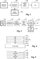
- Fig. 2 is a block diagram illustrating a current ECW fabrication process.
- the outermost glass is cut to size and tempered in 202, which corresponds to an EC glass fabrication process.
- the EC device is fabricated, e.g., so that it has the layer structure shown in Fig. 1 (a) , in 204.
- the EC device is patterned in 206, e.g., to reduce defects and improve yield and appearance.
- Bus bars are added to provide "electrification" (e.g., wiring) for the EC device in 208.
- a second substrate is added in spaced apart relation to the EC device, e.g., as shown in Figs. 1(a) and 1(b) .
- 204, 206, 208, and 210 represent an insulating glass (IG) unit fabrication process.
- This IG unit may ultimately be incorporated into an ECW, e.g., as shown on the left-hand side of Fig. 1(b) .
- the most practical place to have the EC coating is on the inner surface of the outermost lite.
- the placement of bus bars on this surface for electrification presents challenges not only to current IG fabricators, but also to glazers.
- Architects, commercial building owners, and end-users require information about the durability of the EC window over long durations of time.
- the reliability of the IG unit seal therefore is a concern.
- the EC IG unit differs from conventional windows in that interconnections to power the device must pass through the moisture barrier seal. There are no standards for interconnects and feed-throughs that preserve the seal integrity. What is on the market is proprietary. There are also concerns about the durability of the EC film stack when exposed to the range of solar and environmental stresses that a window experiences over its lifetime.
- Certain samples relate to top-down and/or bottom-up changes to (a) materials, (b) the electrochromic device stack, (c) high volume compatible process integration schemes, and (d) high throughput, low cost deposition techniques and equipment. In so doing, certain examples may be used to provide reduced cost EC assemblies, en route to "Net-Zero Energy Buildings.”
- Certain examples involve an optically doped cathode and/or anode for greater visible transmission in the clear state, greater solar heat gain control (SHGC) delta between these states, improved appearance, and better reliability.
- SHGC solar heat gain control
- Controlling the stoichiometry of WO x advantageously may result in improvements with respect to the SHGC delta and better appearance (e.g., in terms of coloration).
- Anodically coloring the counter electrode also may increase the SHGC delta.
- Another aspect of certain examples involves the incorporation of a novel electrochromic device stack.
- a novel electrochromic device stack For example, the inclusion of a low-cost, low-Fe mid-lite substrate may help reduce the need for substrate-device barrier layers.
- An improved transparent current collector (TCC) with much higher conductivity and transmittance than ITO may be provided for increased switching speed and reduced cost.
- TCC transparent current collector
- LiPON lithium phosphorus oxynitride
- the use of transparent dielectric/conductive layers may be used to shift the color based on selective interference in certain examples.
- Still another aspect of certain examples involves novel techniques for electrochromic device integration.
- certain examples may involve the use of laminated/bonded glass for the outer lite of EC IG unit. This may advantageously result in the complete elimination of the use of tempered glass in EC fabrication step, reduce the need for glass sizing and tempering before EC processing, enable the use of a single standard type and sized glass in EC fabrication for best process reproducibility and economy of scale, and/or enable post-EC fabrication sizing of glass. It also may advantageously enable device patterning after all EC layers have been deposited, thereby reducing.the likelihood of defects and improving yield and appearance.
- a novel LiPON deposition source capablee of achieving high deposition rates and modulating growth kinetics may, in turn, enable high throughput and better film characteristics in certain examples.
- Certain examples also may use a novel linear showerhead based Li evaporator with remote, normal ambient compatible Li sources.
- a method of making electrochromic glass units i.e. windows according to appended independent claim 1 is provided.
- a method of making an electrochromic (EC) assembly is provided.
- First, second, and third glass substrates are provided, wherein the second substrate is thermally tempered and the first substrate is not thermally tempered.
- a plurality of EC device layers are sputtering-deposited, directly or indirectly, on the first substrate, with the plurality of EC device layers comprising a first transparent conductive coating (TCC), a counter electrode (CE) layer, ion conductor (IC) layer, an EC layer, and a second TCC.
- TCC transparent conductive coating
- CE counter electrode
- IC ion conductor
- a method of making an electrochromic (EC) assembly is provided.
- a plurality of EC device layers are sputtering-deposited, directly or indirectly, on a first substrate, with the plurality of device layers comprising, in order moving away from the first substrate, a first transparent conductive coating (TCC), a cathode layer, an electrolyte layer, an anodically coloring anode layer, and a second TCC.
- TCC transparent conductive coating
- the first substrate with the plurality of device layers sputter-deposited thereon is connected to a second substrate such that the first and second substrates are in substantially parallel and spaced apart relation to one another.
- an electrochromic (EC) assembly is provided.
- First, second, and third glass substrates are provided, with the second and third substrates being substantially parallel to and spaced apart from one another.
- a plurality of sputter deposited EC device layers are supported by the first substrate, with the plurality of EC device layers comprising a first transparent conductive coating (TCC), a counter electrode (CE) layer, ion conductor (IC) layer, an EC layer, and a second TCC.
- TCC transparent conductive coating
- CE counter electrode
- IC ion conductor
- EC electrochromic
- an electrochromic (EC) assembly is provided. At least first and second glass substrates are provided, with the first and second substrates being substantially parallel to and spaced apart from one another. A plurality of sputter deposited device layers are supported by the first substrate, with the plurality of EC device layers comprising a first transparent conductive coating (TCC), a doped and anodically coloring counter electrode (CE) layer, an ion conductor (IC) layer, a doped EC layer comprising WOx, and a second TCC.
- TCC transparent conductive coating
- CE doped and anodically coloring counter electrode
- IC ion conductor
- an electrochromic device including a plurality of thin-film layers supported by a first substrate.
- the plurality of layers comprises a doped and anodically coloring anode layer; an electrolyte layer comprising Li; and a doped cathode layer comprising WOx.
- Certain example embodiments involve an optically doped cathode and/or anode for greater visible transmission in the clear state, greater solar heat gain control (SHGC) delta between these states, improved appearance, and better reliability.
- SHGC solar heat gain control
- Controlling the stoichiometry of WO x advantageously may result in improvements with respect to the SHGC delta and better appearance (e.g., in terms of coloration).
- Anodically coloring the counter electrode also may increase the SHGC delta.
- Another aspect of certain examples involves the incorporation of a novel electrochromic device stack.
- a novel electrochromic device stack For example, the inclusion of a low-cost, low-Fe mid-lite substrate may help reduce the need for substrate-device barrier layers.
- An improved transparent current collector (TCC) with much higher conductivity and transmittance than ITO may be provided for increased switching speed and reduced cost.
- TCC transparent current collector
- LiPON lithium phosphorus oxynitride
- the use of transparent dielectric/conductive layers may be used to shift the color based on selective interference in certain examples.
- Still another aspect of certain examples involves novel techniques for electrochromic device integration.
- certain examples may involve the use of laminated/bonded glass for the outer lite of EC IG unit. This may advantageously result in the complete elimination of the use of tempered glass in EC fabrication step, reduce the need for glass sizing and tempering before EC processing, enable the use of a single standard type and sized glass in EC fabrication for best process reproducibility and economy of scale, and/or enable post-EC fabrication sizing of glass. It also may advantageously enable device patterning after all EC layers have been deposited, thereby reducing the likelihood of defects and improving yield and appearance.
- a novel LiPON deposition source capable of achieving high deposition rates and modulating growth kinetics may, in turn, enable high throughput and better film characteristics in certain examples Certain examples also may use a novel linear showerhead based Li evaporator with remote, normal ambient compatible Li sources.
- Certain examples involve changes to EC materials, the EC device stack, HVM compatible process integration schemes, and/or high-throughput low cost deposition sources, equipment, and factories. These aspects of certain examples are discussed, in turn, below.
- Certain examples relate to advantages in terms of one or more of cost, device performance, durability, aesthetics, and/or scalability. For example, some current electrochromic products cost more than $50/sq. ft., whereas the techniques of certain examples may provide electrochromic products at a cost that preferably is less than $25/sq. ft., more preferably less than $20/sq. ft., and still more preferably less than $15/sq. ft. Although it is difficult to run wiring and control infrastructure for current products, certain examples may provide for relatively simple modular products, with wireless powering and/or control options.
- delta E may be less than about 1.5, more preferably less than about 1.25, and still more preferably less than about 1.
- certain examples may reduce the yellowish hue in the clear state and the multiple colors that sometimes are present in the tinted state, instead providing a more neutral color in the clear state with a choice from one of multiple colors in the tinted state.
- certain examples may reduce switching uniformity problems, e.g., by causing the latitude to at least appear to change "all at once" (at least as compared to the variability in shade lines and individual controls in current systems).
- current EC devices generally are limited to 1m wide designs, certain examples may scale up to 3.2m wide (or even wider) designs so as to be in-line with commonly available stock glass sheets.
- Fig. 3 is a block diagram illustrating an ECW fabrication process in accordance with an example embodiment.
- the Fig. 3 process differs from the Fig. 2 process in several ways, owing to the fact that the Fig. 3 process is designed to provide an EC device on an EC substrate that may be bonded, laminated, or otherwise connected to a temperable substrate.
- a material such as PVB, EVA, or the like may be used, as may "optibond technology," which is commercially available from Litemax.
- the laminate that is used may incorporate a UV blocker (e.g., a UVA blocker).
- a UVA blocker may be included, with Tuv ⁇ 1%, more preferably ⁇ .75%, and still more preferably ⁇ .5%.
- the UV blocker may a thin film coating comprising one or more of Bi, BiO, Zn, ZnO, TiO, BiSnO, AgO, Ce, CeO, and/or the like.
- a PET coating may be provided, with a UV blocking material provided thereon and/or therein.
- an ITO-coated PET layer may be provided in certain example embodiments. It will be appreciated that organic and/or inorganic materials may be used in connection with certain example embodiments.
- the laminate may be selected so that its refractive index matches with the adjacent layers and/or substrates. This advantageously will help keep reflectance low. Reflectance also may be lowered, e.g., by incorporation of one or more anti-reflective (AR) layers.
- AR anti-reflective
- the EC device is provided on a separate substrate that may be later bonded, laminated, or otherwise connected to a temperable substrate, efficiencies can be realized, e.g., in that larger sheets can be sputter-coated or the like and later cut to size. Example structural details are provided below.
- large size glass is provided in 302.
- An EC device is fabricated according to the example techniques described below in 304. Device patterning and sizing is carried out in 306, thereby forming a plurality of EC devices on a plurality of corresponding EC substrates. As indicated above, this is an advantage over the conventional process shown in Fig. 2 , where individual EC devices are fabricated directly on individually pre-cut individually already-tempered substrates.
- bus bars are connected and the EC device is "electrified" (e.g., wired) in 308.
- the bus bars may be formed by selectively laser etching away layers to carefully expose the TCC.
- both "full” and “half” cuts may be made, e.g., to expose the bottom and top TCCs.
- the laser power may be controlled to selectively remove some or all of the layers in this manner.
- the outer substrate to which the EC device and substrate is to be connected is sized and tempered. Then, in 310, the appropriately sized EC devices are laminated, bonded, or otherwise connected to the appropriately sized outer substrates. The sub-assemblies comprising the EC devices laminated, bonded, or otherwise connected to the outer substrates are then build into corresponding insulating glass (IG) units in 314, e.g., as described in greater detail below.
- IG insulating glass
- Fig. 4 is an illustrative electrochromic substrate and stack helpful to understand the present invention.
- Fig. 4 incorporates an electrochromic stack 400 that is somewhat similar to known electrochromic stacks in that it incorporates conductive layers (TCCs), an electrochromic (EC) layer, a counter electrode (CE) layer, and an ion conductor (IC) layer.
- TCCs conductive layers
- EC electrochromic
- CE counter electrode
- IC ion conductor
- the Fig. 4 electrochromic stack 400 differs from current stacks in terms of materials, overall stack design, and performance characteristics. For example, thermal performance, EC speed, long-term EC reliability, and aesthetics may be improved, e.g., optimize the performance of known materials and develop new material systems that further improve performance of the overall EC device.
- thermal performance, EC speed, long-term EC reliability, and aesthetics may be improved, e.g., optimize the performance of known materials and develop new material systems that further improve performance of the overall EC device
- a first area of innovation involves the cathode/EC and anode/CE electrode materials.
- the thermal performance of an ECW is related to the range of SHGC between clear and tinted states.
- the absorptivity of either or both of the cathode and anode layers may be reduced in the clear state, and/or an anodically coloring counter electrode may be created to lower the transmission (T v ) in the colored state.
- the appropriate material selection may also increase reliability and switching speed.
- a counter electrode typically includes NiO, with Li+ or H+ ions.
- NiO NiO
- Li+ or H+ ions As described above, improving thermal performance, lowering aborptance, and improving reliability and stability of conductive electrode CE are advantageous.
- additives such Mg, Al, Si, Zr, Nb and Ta, a significant reduction of EC and CE film absorptance may be achieved, especially at short wavelengths.
- films containing V and Ag have not show the same improvements in optical properties compared to those of pure nickel oxide.
- Mg and/or other element incorporation in a combinatorial fashion, may be used to optimize its beneficial effect in both NiO and LiNiO systems for widening the band gap and improving the transmittance substantially.
- the inclusion of W into the LiNiO also is possible in certain examples, and it may be used to improve the stability as a CE layer to UV radiation and moisture.
- This and/or other substitutional doping may be used to increase electrical conductivity (in some cases by 3 orders of magnitude, e.g., LiCoO 2 vs. LiCo 0.95 Mg 0.05 O 2 ).
- doping the CE (and/or the IC) with Mg also makes it a "faster" conductor.
- Certain examples also may involve anodically coloring the counter electrode, e.g., for improved thermal performance.
- the CE is used to store the charge, which is in turn used to color the electrochromic layer.
- the CE layer may allow charges to intercalate easily; be stable and durable to repeated cycling; and be very transparent in the clear state; and if possible, display electrochromism when fully discharged of intercalated ions (e.g., anodically).
- the CE may be made electrochromic.
- the CE may be the "reverse" of the EC layer, e.g., such that it becomes transparent with ions, and provides for a color change on ion loss.
- certain examples may incorporate a CE based on NiO systems that have been shown to be stable upon repeated charge insertion/extraction cycling. These systems sometimes display a small amount of residual absorption when the device is fully intercalated, e.g., in Li x NiO (1+y) state in the reaction shown below. The challenge is to remove this absorption without sacrificing the wide dynamic range and good switching kinetics of the device.
- the substitutional doping, analogous to the discussion in previous section, using Li may induce better T v and remedy the small absorbance that is counter to increasing the SHGC delta.
- Li x Ni 1-x O may have a wide optical dynamic range and more neutral color than tungsten oxide, as well as better stability.
- Li x Ni 1-x O may be anodically coloring, thereby providing the advantage of being complementary to cathodic tungsten oxide.
- a combination of these materials may be favorable with regard to electrochemical potentials, and as well as attaining a neutral deeper color in the dark state.
- the photopic coloration efficiency of this anodically coloring material typically is high.
- the absorptivity and/or color modulation of the EC tungsten oxide (WOx) may be altered for thermal performance and appearance.
- Stoichiometric WO 3 films are transparent for energies below the fundamental band gap at ⁇ 3 eV. Li ion intercalation leads to electrochromism manifested by a broad absorption band centered at ⁇ 1.2 eV, which produces a distinctly blue color. This phenomenon may be described in terms of intervalence charge transfer with electrons transferred from a W 5+ site to an adjacent W 6+ site. The effects of polarons may be incorporated into a new model using tight binding approximation.
- the value of x in slightly sub-stoichiometric WO x can be optimized in certain examples so that the EC material is yet more transparent and, upon increased lithiation, increases absorbtivity.
- the sub-stoichiometric value of x preferably is 2.4 ⁇ x ⁇ 3; more preferably 2.6 ⁇ x ⁇ 3.
- a value of about 2.88 has been found to be particularly advantageous. Such values help reduce "yellowness" and improve the depth of color of the EC, which helps improve clear and colored states.
- One solution involves reducing (or minimizing) the amount of blind-charge present in the film by understanding the root cause of the Li "loss.”
- One solution is related to the type of target used in the deposition of the EC material, the addition of an ion beam, and the monitoring of the process to judiciously control the stoichiometry of the films.
- EC films with acceptable electrochromic properties may be deposited from ceramic targets using ion assisted twin magnetron configurations.
- certain examples may employ substitutional doping and grain structure control to modulate the yellowish hue in the clear state.
- ECW is the yellowish baseline color in the clear state. The root causes are thought to be (1) the structural instability of metal oxide units (WO x ) with Li insertion/de-insertion cycles, leading to Jan-Teller distortion and corresponding shift in energy structure and color, (2) the base color of NiO x , the most frequently used base anode material, and (3) interference related to grain boundaries.
- WO x metal oxide units
- Doping with appropriate metals (V, Mo, etc., into NiO x ) and halides (e.g., Cl) may be used in certain examples to address a least the first two root causes to change the band gap (and thus the varied light-material interaction) and/or to enhance the WO x structural stability over Li cycling.
- the grain structure may be modulated by deposition process optimization in certain examples, either with in situ or post-deposition ex situ treatments (e.g., applying substrate bias and microwave enhancements or annealing). This also may be used to enhance the structural stability of WO x over Li cycling.
- the IC helps to maintain internal electrical isolation between the EC and CE electrodes while providing ionic conductance for electrochromic behavior.
- the stability and reliability of electrochromism depends on the properties of the electrolyte.
- Lithium phosphorous oxynitride (LiPON) may be used as the electrolyte layer material in certain example. The choice is based on its superior reliability and stability, as demonstrated in the thin film battery applications.
- LiPON is an electrically insulating material (> 1E14 ⁇ -cm), so RF sputtering is traditionally used and it exhibits a low deposition rate ( ⁇ 1 ⁇ m/hr). This low deposition rate may be improved as discussed below, and/or other materials and methods that are more amenable to high throughput production may be used in connection with certain examples.
- the leakage current can be split into contributions that are associated with the thin film stack itself (diffusion limited), and that are associated with localized point defects, (both bulk and interfacial).
- the forward and reverse barrier heights for the EC/CE junction may be optimized by altering the composition, structure, and interface chemistry of the IC. The evidence suggests that leakage current may be reduced to negligible levels through selection of appropriate process and materials for the IC layer. Accordingly, certain examples provide an IC layer where the integrity of the electron barrier structure is maintained with adequate ionic conductivity.
- the EC device stack 400 may include a first transparent conductive coating (TCC) 404, a counter electrode layer 406, an ion conductor layer 408, an electrochromic layer 410, and a second TCC 412.
- TCC transparent conductive coating
- Each of the first and second TCCs 404 and 412 may be about 200 nm thick in certain examples.
- An example layer system for one or both of the TCCs is provided below, e.g., in connection with Fig. 5 .
- the anodic CE layer 406 may be about 100-400 nm thick, and it may include NiO and contain Li+ or H+ ions.
- a LiPON-based IC/electrolyte layer 408 may be about 1-3 microns.
- the EC layer 410 may be 100-400 nm thick. Either or both of the CE layer 406 and the EC layer 410 may be doped, e.g., to provide for better and/or deeper coloration.
- a barrier layer (not shown in the Fig. 4 example) may be provided over the outermost TCC 412, and such a barrier layer may enable color shift. In certain examples, the outermost TCC 412 itself may enable color shift.
- the EC device stack 400 is provided on an EC substrate 402 which may, in certain examples, be provided as a standard size/thickness large substrate.
- the EC substrate 402 may be a low iron, non-tempered substrate that is cut after the EC device is fabricated on it.
- Example low-iron glass substrates are disclosed in, for example, U.S. Application Serial No. 12/385,318 , as well as in U.S. Publication Nos. 2006/0169316 ; 2006/0249199 ; 2007/0215205 ; 2009/0223252 ; 2010/0122728 ; and 2009/0217978 .
- the EC device stack design shown in Fig. 4 and described herein differs from current designs in a number of respects including, for example, the use of the novel transparent conductor described below, multiple dielectric layers for interferometric color shift, low Fe and low cost substrates on which the EC layers are formed, LiPON as the electrolyte, and stack thickness optimization. These factors each affect transmittance, color, transition speed and cost, as described elsewhere.
- the switching speed of an EC device is limited by the sheet resistance of the TCO layers, although voltage drop in the EC layer also contributes to delays. This is because the voltage that can be applied to the device is fixed, and the amount of charge that must be transferred in order to fully color the device scales with the area. Given a series of devices of fixed length, but with progressively larger widths, as the separation between the bus bars gets larger, the impedance of the EC stack itself (the part of the device where the current travels perpendicular to the surface of the glass) gets smaller. In contrast, the impedance of the TCO layers where the current is flowing parallel to the surface of the glass gets larger. Overall, this change in area leads to a larger potential drop in the TCO layers. This results in a lower potential applied directly to the stack, leading to slower switching. Thus, it will be appreciated that to increase the switching speed of reasonably sized devices, e.g., suitable for architectural applications, the conductivity of the TCO layers may be increased.
- Such stacks may have sheet resistances at least one order of magnitude lower than those of currently available TCOs. Additional advantages of this coating include its "low-E” functionality, which helps improve SHGC and UV protection of the active layers.
- Fig. 5 is an illustrative transparent conductive coating (TCC) usable in connection with certain examples.
- the example TCC of Fig. 5 includes a silver-based layer 506, sandwiched by first and second ITO layers 502 and 510.
- First and second interlayers 504 and 508 may be provided between the silver-based layer 506 and the first and second ITO layers 502 and 510.
- Such interlayers may comprise NiCr (e.g., NiCrOx) and/or Cu.
- the silver-based layer 506 preferably is 100-200 angstroms thick, more preferably 120-180 angstroms thick, and sometimes 140 angstroms thick.
- Each ITO layer preferably is 1000-2000 angstroms thick, more preferably 1200-1600 angstroms thick, and sometimes about 1400 angstroms thick.
- the interlayers preferably are 1-20 angstroms thick, more preferably 5-15 angstroms thick, and sometimes 10 angstroms thick.
- the visible transmission of such layers may be optimized to provide visible transmission of preferably 65%, more preferably 75%, still more preferably 80%, and sometimes as high as 85% or higher.
- low-E coatings may be provided between a glass substrate and the lower-most ITO layer in certain examples.
- Such low-E coatings may include layers with alternating high and low indexes of refraction, e.g., in a high-low-high-low-high arrangement.
- Fig. 5 shows a simple TCC layer stack, other layer stacks also are possible.
- a suitable TCC layer stack may include 2, 3, 4, or more of the layer stack shown in Fig. 5 .
- the TCCs may be graphene- and/or CNT-based. See, for example, U.S. Application Serial Nos. 12/461,349 and 12/659,352 .
- a color shifting layer stack may be deposited adjacent to the EC coating stack, and it may comprise sputterable insulating and metallic layers.
- the optical properties as well as thickness of the individual layers may be engineered to provide functionality including, for example, enhanced solar performance, visible color coordinate shifts into a more desirable neutral tone both in the un-tinted and tinted states, and UV screening to the underlying EC stack, thus prolonging its life.
- these layers may increase the reliability of the EC window, e.g., by functioning as a barrier for ambient oxidants when and if the seal in the IG unit breaks down. It is also feasible to use the TCC, discussed above to accomplish this functionality.
- a thin barrier layer such as a silicon nitride inclusive (e.g., Si 3 N 4 or other suitable stoichiometry) layer.
- a low Fe, lower cost glass product may reduce and sometimes even eliminate the need for a barrier layer, thereby leading to a reduction in process complexity, improvement in transparency, and lowering EC manufacturing costs.
- LiPON as the IC layer advantageously increases device reliability.
- reliability is increased at least in terms of life cycle by using the most robust and electrochemically stable electrolyte, (LiPON), which is stable up to 5.5V and against Li metal and whose life cycle in thin film battery application has been demonstrated to be over 100,000 cycles with minimal losses in capacity.
- Minimal capacity loss for the battery may translate to a reduced shift in optical properties in electrochromics.
- Stack thickness may be optimized in certain examples to improve the switching speed of the EC device. For example, one way to improve the EC device speed is to reduce the thickness of the CE and IC layers. The rate of switching has been found to increase with increases in lithium levels. However, it also has been found that if the lithium level is increased too far, the devices become electronically "leaky,” thereby failing to become fully colored and also failing to reduce the rate of switching. The stack materials and thickness ranges specified above have been found to be advantageous in terms of improve switching speed, although it is also possible to adjust the thicknesses and materials in other ways in different examples.
- certain example embodiments instead involve lamination, a non-tempered single type of glass for EC fabrication, post-EC fabrication glass sizing, and device patterning after blanket deposition of EC layers. From the Fig. 3 schematic and description provided above, it will be appreciated that there is an absence of tempering, along with the inclusion of lamination steps.
- the outer window glass includes a two-sheet glass unit.
- a first sheet is provided for use as the EC sheet, and the other sheet is provided to meet the tempering/safety and other product requirements.
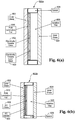
- This arrangement is shown in Figs. 6(a) and 6(b) , which show cross-sectional views for IG units prodicible in accordance with certain example embodiments. It will be appreciated from Figs. 6(a) and 6(b) that there are at least two options for bonding the EC glass.
- the EC stack faces the open inner space, whereas the EC stack is directly bonded to the outer lite in the example illustrated in Fig. 6(b) .
- Fig. 6(b) is particularly advantageous in that it is perhaps better protected from the breach of IG unit seal.
- One advantageous consequence of this lamination/bonded concept is that the tempering requirement for the glass used for EC device fabrication can sometimes be completely eliminated. This, in turn, opens the door to using single type substrates and post-fabrication glass sizing with non-tempered glass, consistent and compatible with the current fabrication flows of coated glass and windows. Consequently, this helps lead to a robust and stable production environment for optimal process control, throughput and yield, and to lower cost.
- the IG units 600a and 600b shown in Figs. 6(a) and 6(b) are similar to one another. Both include outer glass substrates 602 that may be tempered, along with inner glass substrates 604. These substrates 602 and 604 are substantially parallel to one another and spaced apart, e.g., using spacers 606, thus forming an isolation gap 608.
- a laminate 610 e.g., a PVB lamination foil, an EVA laminate, an optibond laminate, etc. helps connect the outer glass substrate 602 to the EC glass 402. In Fig. 6(a) , the laminate 610 connects the outer glass substrate 602 to the EC glass substrate 402 so that the EC layer stack 400 faces the isolation gap 608.
- the laminate 610 connects outer glass substrate 602 to the EC glass substrate 402 so that the EC layer stack 400 is provided between these two substrates 602 and 402.
- Some or all of the substrates may be UltraWhite glass substrates, which are commercially available from the assignee of the instant invention.
- the integration modification to pattern the device after all EC layers are deposited is another advantage of certain examples, e.g., as compared to the conventional process shown in Fig. 2 , where multiple device patterning was needed, e.g., as indicated by the bi-directional arrow.
- the EC integration flow that includes lamination, bonding, or other connection of two glass sheets to form a single outer lite of an IG unit, as illustrated in Figs. 6(a) and 6(b) for example, may lead to additional benefits.
- such designs have the potential for broadening the product applications, e.g., by flexibly combining the standard EC glass with any another glass product whose properties can be selected to meet the desired window requirements, including safety, color, sound barrier, and others. This process flow is consistent with the current value chain of the glass industry and would help broader the applicable application areas to further amortize the development and cost.
- the lamination, bonding, and/or other connection of glass units in certain examples may be similar to those techniques used in both glass (safety products, etc.) and thin-film solar photovoltaic industries.
- Challenges related to thermal cycling and actual temperature to which the "absorptive" EC device can be subjected may be mitigated, e.g., by selecting the materials so that they match with one another (e.g., in terms of coefficient of thermal expansion, etc.) to help ensure compatibility in potentially harsh environments.
- Fig. 7 is a third illustrative electrochromic insulating glass (IG) unit producible in accordance with an example embodiment.
- the example illustrated in Fig. 7 is similar to the Fig. 6(b) in that sputter-deposited EC layers 400 are disposed between the outer glass substrate 602 and the mid-lite 402.
- the example illustrated in Fig. 7 differs from the example illustrated in Fig. 6(b) in that it includes a number of optional low-E coatings.
- first low-E coating 702 located on an inner surface of the outer glass substrate 602, second and third low-E coatings 704 and 706 located on opposing surfaces of the mid-lite 402, and a fourth low-E coating 708 on the surface of the inner substrate 604 facing the air gap 608.
- first low-E coating 702 located on an inner surface of the outer glass substrate 602
- second and third low-E coatings 704 and 706 located on opposing surfaces of the mid-lite 402
- fourth low-E coating 708 on the surface of the inner substrate 604 facing the air gap 608.
- One or more of the optional low-E coatings may be the SunGuard SuperNeutral 70 (SN70) low-E coating commercially available from the assignee, although other low-E coatings also may be used. For example, see U.S. Patent Nos.
- Certain example embodiments make EC technology more cost-effective by providing high deposition rate deposition sources to allow high throughput, low capital intensive EC factories.
- the table below identifies possible deposition methods for the EC layers usable in connection with certain example embodiments.
- There are two basic approaches for the lithiated layers namely, single step deposition from a composite target or sequential deposition of oxide and lithium.
- Using highly reactive Li in a manufacturing environment may be problematic.
- using a lithiated target may lead to inconsistency in stoichiometry over the target lifetime, when a sputtering method is used.
- certain example embodiments may implement a two-step method.
- Step 1 Step 2 Target Sputtering Type Target Sputtering Type Li x M y O z Li x M y O z pDC or RF in Ar ambient N/A N/A Li x M y O z M y O z pDC or RF in Ar/O 2 Li Evap or Sputt in Ar Li x M y O z M DC or pDC in Ar/O 2 Li Evap or Sputt in Ar LiPON Li 3 PO 4 RF (in nitrogen ambient) N/A N/A TaO x Ta 2 O 5 pDC or RF in Ar then O 2 N/A N/A TaO x Ta DC or pDC in O 2 N/A N/A
- LiPON electrolyte may be used in certain examples, because of its superior reliability and stability as demonstrated in the thin film battery applications.
- LiPON is an electrically insulating material (greater than 1E14 ⁇ -cm), so conventional RF sputtering typically exhibits a low deposition rate (less than 1 ⁇ m/hr). Conventional deposition of Li by evaporation is also slow. Accordingly, certain example embodiments may be sped-up so as to be compatible with a high throughput and large area coating system.
- certain example embodiments may implement a multi-frequency based plasma deposition source, in which higher frequency plasma is superimposed with the common RF power. This may enhance the control of plasma density and sheath voltage. It also may increase the deposition rate, as well as impart energy onto the growing film, e.g., to modulate growth kinetics. This may also affect conformality, morphology, crystallinity, and low pinhole density to yield films with better coating characteristics. This, in turn, will allow the use of thinner electrolytes, leading to higher manufacturing throughput, and lower impedance EC device with faster device switching speeds.
- Fig. 8(a) is an SEM image of a 600 nm Al layer deposited by conventional evaporation. The image in Fig.
- Fig. 8(a) reveals a columnar structure having a rough surface.
- Fig. 8(b) is an SEM image of a 600 nm A1 layer deposited using a plasma-activated evaporation in accordance with certain example embodiments. That is, Fig. 8(b) shows a multi-plasma sputtering concept for RF-HF combination source. The SEM photograph in Fig. 8(b) shows an example of the effects of imparting energy onto a growing film, which include a denser structure having a smooth surface.
- Li sputtering issues with “clustering" and low deposition rate, which negatively affect the uniformity. Clustering occurs when the sputtering species is much heavier (e.g., Ar) and the sheath voltage is too high leading to high momentum. Use of lower atomic weight He and Ne will both reduce the deposition rate and incur high cost. Consequently, a multiple-frequency plasma source, analogous to the one proposed for LiPON deposition, may be used in certain example embodiments. However, RF may be superimposed upon DC sputtering to increase the plasma density and to reduce the sheath voltage. This will allow the use of lower cost Ar while also reducing clustering.
- RF may be superimposed upon DC sputtering to increase the plasma density and to reduce the sheath voltage. This will allow the use of lower cost Ar while also reducing clustering.
- time savings may be realized in certain example embodiments, as active layers may be processed in a single integrated deposition system where the substrates see only the clean deposition chambers, thereby reducing yield- and aesthetics-affecting defects/debris caused by, for example, patterning, substrate sizing, exposure to air, etc.
- the limited air exposure also reduces clean-room requirement and once again leads to overall cost reduction.
- the EC layer stack process may be sped up at least 2 times compared to current practices, more preferably at least 3 times, and still more preferably at least 5 times.
- Multiple targets e.g., 2, 3, 4, or even 5 or more targets may be used in the deposition process to increase line speed.
- An example EC IG unit includes a tempered outer substrate, a mid-lite, and an inner substrate.
- the outer substrate is a 6mm thick UltraWhite substrate
- the mid-lite is a 1mm thick Ultra White substrate.
- the outer substrate and the mid-lite are bonded together using an optibond laminate.
- Electrochromic layers are disposed on the surface of the mid-lite that face the outer substrate.
- the TCCs used in connection with the electrochromic layers correspond to the Fig. 5 example layer stack.
- a SunGuard SuperNeutral 70 low-E coating commercially available from the assignee is formed on both sides of the electrochromic layers.
- the inner susbtrate is a 6mm thick sheet of Clear glass, commercially available from the assignee.
- An air gap of 12mm is present between the mid-light and the inner substrate.
- This arrangement may have the following example properties: Condition Visible Light Solar Energy (Direct) Winter Summer LSG %T %Reflectance %T % R Out U-value U-value Shading Coef. SHGC RHG Indoor Outdoor Night Day Untinted LiPON 48 15 18 15 43 .291 .28 .22 .35 49 2.03 Tinted LiPON 2 11 9 1 40 .291 .28 .07 .062 17 .36 As is known, LSG stands for light-to-solar gain. In the table above, "% R Out” refers to the percent of direct solar energy reflected out.
- transmission in the tinted state preferably is less than 5%, more preferably less than 4%, still more preferably less than 3%, and sometimes even about 2%.
- transmission in the untinted state preferably is at least about 40%, more preferably at least about 45%, and sometimes 48% or even higher.
- SHGC preferably ranges from .03 to .5.
- a first layer may be said to be “on” or “supported by” a second layer, even if there are one or more layers therebetween.
Claims (10)
- Procédé de fabrication d'unités de vitrage isolant électrochromes, le procédé comprenant :la fourniture (302) d'un premier substrat de verre (402) ;la mise en place (304) de couches d'un composant électrochrome sur le premier substrat, comprenant au moins une couche de contre-électrode -CE- (406), une couche conductrice d'ions -IC- (408) et une couche électrochrome -EC- (410), et des premier et second revêtements conducteurs transparents -TCC- (404, 412) formant les couches extérieures opposées des couches du composant électrochrome ;la structuration (306) des couches du composant électrochrome et le découpage du premier substrat de verre (402) sur lequel sont déposées les couches du composant électrochrome, de façon à former une pluralité de substrats du composant électrochrome (402) ;la fourniture d'une pluralité de seconds substrats de verre (402) ayant subi une trempe thermique ;le contrecollage ou le collage (312) de la pluralité de substrats (402) du composant électrochrome respectivement à la pluralité de deuxièmes substrats de verre (602) ;la fourniture d'une pluralité de troisièmes substrats de verre (604) ;la formation d'une pluralité d'unités de vitrage isolant -IG- électrochromes (600a, 600b), chacune comprenant un substrat (402) du composant électrochrome et un second substrat (602), sensiblement parallèle au troisième substrat de verre (604) et écarté de ce dernier.
- Procédé selon la revendication 1, dans lequel les couches (406, 408, 410) du composant électrochrome sont déposées par pulvérisation cathodique, la pulvérisation cathodique étant de préférence assistée par un faisceau d'ions.
- Procédé selon la revendication 1, dans lequel les couches (406, 408, 410) du composant électrochrome sont en regard des deuxièmes ou des troisièmes substrats (602, 604) après assemblage dans les unité de vitrage IG (600a, 600b).
- Procédé selon la revendication 1, dans lequel chacun desdits TCC (404, 412) comprend une couche d'argent (506) intercalée entre les couches d'ITO (502, 510), et en outre dans lequel des couches (504, 508) contenant du NiCr, ou en Cu, sont disposées entre la couche d'argent (506) et les couches d'ITO (502, 510), de préférence dans lequel la résistance de feuille de chacun desdits TTC (404, 412) est d'environ 5 ohms/carré.
- Procédé selon la revendication 1, dans lequel la couche conductrice d'ions (408) comprend du LiPON.
- Procédé selon la revendication 1, dans lequel la couche électrochrome (410) comprend de l'oxyde de tungstène.
- Procédé selon la revendication 6, dans lequel l'oxyde de tungstène est sous-stoechiométrique.
- Procédé selon la revendication 7, dans lequel l'oxyde de tungstène sous-stoechiométrique WOx présente une valeur sous-stoechiométrique x comprise dans la plage 2,6<x<3.
- Procédé selon la revendication 6, dans lequel la couche de contre-électrode (406), la couche conductrice d'ions (408) et/ou la couche électrochrome (410) sont dopées avec du Mg, le procédé comprenant de préférence en outre :
la fourniture d'un ou plusieurs revêtements à faible émissivité (702, 704, 706, 708), les revêtements à faible émissivité étant prévus sur les surfaces intérieures des deuxièmes substrats (602), sur l'une des surfaces du premier substrat (402) ou sur les deux, et/ou sur les surfaces intérieures des troisièmes substrats de verre (604), plus particulièrement comprenant en outre la fourniture de revêtements (702) bloquant les UV sur les surfaces intérieures des deuxièmes substrats (602). - Procédé selon la revendication 1, dans lequel la pluralité de substrats (402) du composant électrochrome sont contrecollés ou collés à la pluralité de deuxièmes substrats de verre (602), par l'intermédiaire de couches respectives (610) à base d'un polymère.
Priority Applications (1)
| Application Number | Priority Date | Filing Date | Title |
|---|---|---|---|
| PL10757863T PL2470954T3 (pl) | 2009-08-27 | 2010-08-24 | Metoda wytwarzania okien elektrochromatycznych |
Applications Claiming Priority (3)
| Application Number | Priority Date | Filing Date | Title |
|---|---|---|---|
| US23758009P | 2009-08-27 | 2009-08-27 | |
| US12/805,145 US8858748B2 (en) | 2009-08-27 | 2010-07-14 | Electrochromic devices, assemblies incorporating electrochromic devices, and/or methods of making the same |
| PCT/US2010/002332 WO2011028254A2 (fr) | 2009-08-27 | 2010-08-24 | Dispositifs électrochromes, ensembles incorporant des dispositifs électrochromes et/ou leurs procédés de réalisation |
Publications (2)
| Publication Number | Publication Date |
|---|---|
| EP2470954A2 EP2470954A2 (fr) | 2012-07-04 |
| EP2470954B1 true EP2470954B1 (fr) | 2018-12-05 |
Family
ID=43623078
Family Applications (2)
| Application Number | Title | Priority Date | Filing Date |
|---|---|---|---|
| EP10757862.7A Active EP2470953B1 (fr) | 2009-08-27 | 2010-08-24 | Dispositif électrochrome et assemblage l'incorporant |
| EP10757863.5A Active EP2470954B1 (fr) | 2009-08-27 | 2010-08-24 | Procede de fabrication des vitrages electrochromes |
Family Applications Before (1)
| Application Number | Title | Priority Date | Filing Date |
|---|---|---|---|
| EP10757862.7A Active EP2470953B1 (fr) | 2009-08-27 | 2010-08-24 | Dispositif électrochrome et assemblage l'incorporant |
Country Status (12)
| Country | Link |
|---|---|
| US (4) | US8858748B2 (fr) |
| EP (2) | EP2470953B1 (fr) |
| JP (2) | JP5581387B2 (fr) |
| BR (2) | BR112012007879B1 (fr) |
| ES (2) | ES2596652T3 (fr) |
| IN (2) | IN2012DN01735A (fr) |
| MX (2) | MX2012002443A (fr) |
| PL (2) | PL2470953T3 (fr) |
| RU (2) | RU2531063C2 (fr) |
| TR (1) | TR201902917T4 (fr) |
| TW (2) | TWI542934B (fr) |
| WO (2) | WO2011028254A2 (fr) |
Families Citing this family (104)
| Publication number | Priority date | Publication date | Assignee | Title |
|---|---|---|---|---|
| US7593154B2 (en) * | 2005-10-11 | 2009-09-22 | Sage Electrochromics, Inc. | Electrochromic devices having improved ion conducting layers |
| US9136569B2 (en) | 2008-05-21 | 2015-09-15 | Applied Materials, Inc. | Microwave rapid thermal processing of electrochemical devices |
| US9782949B2 (en) | 2008-05-30 | 2017-10-10 | Corning Incorporated | Glass laminated articles and layered articles |
| US8514476B2 (en) | 2008-06-25 | 2013-08-20 | View, Inc. | Multi-pane dynamic window and method for making same |
| US9261751B2 (en) | 2010-04-30 | 2016-02-16 | View, Inc. | Electrochromic devices |
| US10261381B2 (en) | 2009-03-31 | 2019-04-16 | View, Inc. | Fabrication of low defectivity electrochromic devices |
| US10591795B2 (en) | 2009-03-31 | 2020-03-17 | View, Inc. | Counter electrode for electrochromic devices |
| US8582193B2 (en) | 2010-04-30 | 2013-11-12 | View, Inc. | Electrochromic devices |
| US10852613B2 (en) | 2009-03-31 | 2020-12-01 | View, Inc. | Counter electrode material for electrochromic devices |
| US10156762B2 (en) | 2009-03-31 | 2018-12-18 | View, Inc. | Counter electrode for electrochromic devices |
| US11187954B2 (en) | 2009-03-31 | 2021-11-30 | View, Inc. | Electrochromic cathode materials |
| US8432603B2 (en) * | 2009-03-31 | 2013-04-30 | View, Inc. | Electrochromic devices |
| US9723723B2 (en) | 2009-03-31 | 2017-08-01 | View, Inc. | Temperable electrochromic devices |
| FR2948356B1 (fr) * | 2009-07-22 | 2011-08-19 | Saint Gobain | Dispositif electrochrome |
| US20110030290A1 (en) * | 2009-08-07 | 2011-02-10 | Slovak Steven M | Energy efficient fenestration product with suspended particle device |
| US8858748B2 (en) | 2009-08-27 | 2014-10-14 | Guardian Industries Corp. | Electrochromic devices, assemblies incorporating electrochromic devices, and/or methods of making the same |
| US11732527B2 (en) | 2009-12-22 | 2023-08-22 | View, Inc. | Wirelessly powered and powering electrochromic windows |
| US11314139B2 (en) | 2009-12-22 | 2022-04-26 | View, Inc. | Self-contained EC IGU |
| US8213074B1 (en) | 2011-03-16 | 2012-07-03 | Soladigm, Inc. | Onboard controller for multistate windows |
| WO2011087726A2 (fr) | 2009-12-22 | 2011-07-21 | Soladigm, Inc. | Fenêtres électrochcromiques à alimentation sans fil |
| US11342791B2 (en) | 2009-12-22 | 2022-05-24 | View, Inc. | Wirelessly powered and powering electrochromic windows |
| US10303035B2 (en) | 2009-12-22 | 2019-05-28 | View, Inc. | Self-contained EC IGU |
| ES2450520T5 (es) | 2010-03-05 | 2017-08-07 | Sage Electrochromics, Inc. | Laminado de un dispositivo electrocrómico a sustratos de vidrio |
| US9759975B2 (en) | 2010-04-30 | 2017-09-12 | View, Inc. | Electrochromic devices |
| FR2962682B1 (fr) | 2010-07-16 | 2015-02-27 | Saint Gobain | Vitrage electrochimique a proprietes optiques et/ou energetiques electrocommandables |
| US8270059B2 (en) | 2010-08-05 | 2012-09-18 | Soladigm, Inc. | Multi-pane electrochromic windows |
| US20220032584A1 (en) * | 2010-11-08 | 2022-02-03 | View, Inc. | Electrochromic window fabrication methods |
| US8164818B2 (en) | 2010-11-08 | 2012-04-24 | Soladigm, Inc. | Electrochromic window fabrication methods |
| US9958750B2 (en) | 2010-11-08 | 2018-05-01 | View, Inc. | Electrochromic window fabrication methods |
| US9442339B2 (en) | 2010-12-08 | 2016-09-13 | View, Inc. | Spacers and connectors for insulated glass units |
| CN112731720A (zh) | 2010-12-08 | 2021-04-30 | 唯景公司 | 绝缘玻璃装置的改良隔板 |
| US10180606B2 (en) | 2010-12-08 | 2019-01-15 | View, Inc. | Connectors for smart windows |
| US8643933B2 (en) | 2011-12-14 | 2014-02-04 | View, Inc. | Connectors for smart windows |
| US10175549B2 (en) | 2011-03-16 | 2019-01-08 | View, Inc. | Connectors for smart windows |
| US9454055B2 (en) | 2011-03-16 | 2016-09-27 | View, Inc. | Multipurpose controller for multistate windows |
| US10429712B2 (en) | 2012-04-20 | 2019-10-01 | View, Inc. | Angled bus bar |
| WO2012162502A1 (fr) * | 2011-05-26 | 2012-11-29 | Sage Electrochromics, Inc. | Barre omnibus en pont pour dispositifs électrochromes |
| EP2724194B1 (fr) * | 2011-06-21 | 2019-01-09 | View, Inc. | Dispositifs électrochromiques aptes à être trempés |
| FR2977040B1 (fr) * | 2011-06-23 | 2013-06-14 | Saint Gobain | Procede de fabrication d'un dispositif electrochimique a proprietes de transmission optique et/ou energetique electrocommandables |
| JP2014525607A (ja) * | 2011-08-26 | 2014-09-29 | ザ リージェンツ オブ ザ ユニバーシティ オブ カリフォルニア | ナノ構造を持つ透明な導電性酸化物のエレクトロクロミックデバイス |
| US9885934B2 (en) | 2011-09-14 | 2018-02-06 | View, Inc. | Portable defect mitigators for electrochromic windows |
| WO2013039915A1 (fr) * | 2011-09-14 | 2013-03-21 | Soladigm, Inc. | Appareil d'atténuation de défauts portatif pour fenêtres électrochromiques |
| CA2859023C (fr) * | 2011-12-12 | 2023-08-22 | View, Inc. | Dispositifs en couches minces et fabrication de ceux-ci |
| US10739658B2 (en) | 2011-12-12 | 2020-08-11 | View, Inc. | Electrochromic laminates |
| US11048137B2 (en) | 2011-12-12 | 2021-06-29 | View, Inc. | Thin-film devices and fabrication |
| US10606142B2 (en) | 2011-12-12 | 2020-03-31 | View, Inc. | Thin-film devices and fabrication |
| US11865632B2 (en) | 2011-12-12 | 2024-01-09 | View, Inc. | Thin-film devices and fabrication |
| US10295880B2 (en) | 2011-12-12 | 2019-05-21 | View, Inc. | Narrow pre-deposition laser deletion |
| US20210394489A1 (en) | 2011-12-12 | 2021-12-23 | View, Inc. | Thin-film devices and fabrication |
| US10802371B2 (en) | 2011-12-12 | 2020-10-13 | View, Inc. | Thin-film devices and fabrication |
| US11719039B2 (en) | 2011-12-14 | 2023-08-08 | View, Inc. | Connectors for smart windows |
| US11635666B2 (en) | 2012-03-13 | 2023-04-25 | View, Inc | Methods of controlling multi-zone tintable windows |
| EP3410183B1 (fr) | 2012-03-13 | 2022-06-15 | View, Inc. | Atténuation de défauts visibles pour fenêtres électrochromes |
| US9341912B2 (en) | 2012-03-13 | 2016-05-17 | View, Inc. | Multi-zone EC windows |
| IN2014DN08858A (fr) | 2012-04-05 | 2015-05-22 | Sage Electrochromics Inc | |
| JP2013254196A (ja) * | 2012-05-11 | 2013-12-19 | Ricoh Co Ltd | エレクトロクロミック表示装置 |
| US10583523B2 (en) | 2012-05-18 | 2020-03-10 | View, Inc. | Circumscribing defects in optical devices |
| US11255120B2 (en) | 2012-05-25 | 2022-02-22 | View, Inc. | Tester and electrical connectors for insulated glass units |
| KR20150032312A (ko) * | 2012-06-26 | 2015-03-25 | 어플라이드 머티어리얼스, 인코포레이티드 | 전기화학 디바이스들의 마이크로파 급속 열 프로세싱 |
| US10288971B2 (en) | 2012-08-23 | 2019-05-14 | View, Inc. | Photonic-powered EC devices |
| US9158172B2 (en) * | 2012-11-14 | 2015-10-13 | Sage Electrochromics, Inc. | Color matched coating for bus bars |
| CN105324706B (zh) * | 2013-01-21 | 2018-07-24 | 基内斯恰技术股份有限公司 | 电致变色锂镍第五族混合金属氧化物 |
| RU2678028C2 (ru) * | 2013-06-18 | 2019-01-22 | Вью, Инк. | Электрохромные устройства непрямоугольных форм |
| US11891327B2 (en) | 2014-05-02 | 2024-02-06 | View, Inc. | Fabrication of low defectivity electrochromic devices |
| US10294415B2 (en) | 2014-06-09 | 2019-05-21 | iGlass Technology, Inc. | Electrochromic composition and electrochromic device using same |
| US10344208B2 (en) | 2014-06-09 | 2019-07-09 | iGlass Technology, Inc. | Electrochromic device and method for manufacturing electrochromic device |
| US10345671B2 (en) | 2014-09-05 | 2019-07-09 | View, Inc. | Counter electrode for electrochromic devices |
| US10228601B2 (en) | 2014-11-26 | 2019-03-12 | View, Inc. | Counter electrode for electrochromic devices |
| JP7067833B2 (ja) * | 2014-11-26 | 2022-05-16 | ビュー, インコーポレイテッド | エレクトロクロミックデバイス用の対電極 |
| WO2016100075A1 (fr) | 2014-12-15 | 2016-06-23 | View, Inc. | Joints pour fenêtres électrochromiques |
| EP4120012A1 (fr) * | 2014-12-19 | 2023-01-18 | View, Inc. | Atténuation des défauts dans un dispositif électrochromique sous une barre omnibus |
| US10316581B1 (en) | 2015-01-12 | 2019-06-11 | Kinestral Technologies, Inc. | Building model generation and intelligent light control for smart windows |
| US9658508B1 (en) | 2015-01-12 | 2017-05-23 | Kinestral Technologies, Inc. | Manufacturing methods for a transparent conductive oxide on a flexible substrate |
| RU2609599C2 (ru) * | 2015-04-14 | 2017-02-02 | Федеральное государственное унитарное предприятие "Научно-исследовательский институт прикладной акустики" | Противоэлектрод для электрохромного устройства и способ его изготовления |
| US9951552B2 (en) | 2015-05-26 | 2018-04-24 | Guardian Glass, LLC | Glazing with heat flux sensor and/or methods of making the same |
| LT6395B (lt) | 2015-07-24 | 2017-06-12 | Kauno technologijos universitetas | Mikroorganizmų augimo greičio automatinė valdymo sistema ir būdas |
| EP3332288B1 (fr) * | 2015-08-07 | 2020-10-07 | Kinestral Technologies, Inc. | Ensembles formant dispositifs électrochromes |
| US10597518B2 (en) | 2016-04-15 | 2020-03-24 | Furcifer Inc. | Solid polymer electrolyte for electrochromic devices |
| US10392301B2 (en) | 2016-04-15 | 2019-08-27 | Furcifer Inc. | Integration of electrochromic films on a substrate |
| CN109073949B (zh) | 2016-04-19 | 2022-01-11 | Sage电致变色显示有限公司 | 包括透明导电氧化物层和汇流条的电致变色装置和其形成方法 |
| KR102336524B1 (ko) * | 2016-05-20 | 2021-12-07 | 젠텍스 코포레이션 | 전압 균일화를 위한 저항성 코팅 |
| EP3469419B1 (fr) * | 2016-06-14 | 2023-11-29 | Furcifer Inc. | Intégration de films électrochromiques sur un substrat |
| WO2017218705A1 (fr) * | 2016-06-17 | 2017-12-21 | View, Inc. | Atténuation des défauts dans un dispositif électrochrome sous une barre omnibus |
| SG11201802760PA (en) * | 2016-11-11 | 2018-06-28 | Zhuhai Singyes New Materials Technology Co Ltd | Smart glass fixed door of multimedia system of platform screen door |
| RU2649062C1 (ru) * | 2016-12-07 | 2018-03-29 | Федеральное государственное бюджетное учреждение науки Физический институт им. П.Н. Лебедева Российской академии наук (ФГБУН ФИАН) | Оптический модулятор |
| JP7152407B2 (ja) | 2017-02-08 | 2022-10-12 | カーディナル アイジー カンパニー | フィルムからガラスへ切り替え可能なガラス |
| US11320713B2 (en) | 2017-02-16 | 2022-05-03 | View, Inc. | Solar power dynamic glass for heating and cooling buildings |
| JP2020508491A (ja) | 2017-02-27 | 2020-03-19 | セイジ・エレクトロクロミクス,インコーポレイテッド | 基板および透明導電層を含む電気デバイスおよびその形成プロセス |
| RU2676807C9 (ru) * | 2017-06-07 | 2019-03-19 | Общество с ограниченной ответственностью "СмартЭлектроГласс" | Электрохромное устройство и способ его изготовления |
| US11015384B2 (en) | 2017-06-08 | 2021-05-25 | Apple Inc. | Light transmitting panel with active components |
| EP3418795A1 (fr) * | 2017-06-22 | 2018-12-26 | Essilor International | Dispositif multifonctionnel destiné à une lentille ophtalmique |
| WO2019050530A1 (fr) | 2017-09-08 | 2019-03-14 | Guardian Glass, LLC | Dispositif électrochrome durable comprenant un film d'oxyde de tungstène préparé dans un environnement de bombardement ionique élevé et de dépôt basse pression et ses procédés de fabrication |
| EP3682295B1 (fr) | 2017-09-12 | 2023-09-06 | Sage Electrochromics, Inc. | Dispositif à transmission variable non électroluminescent et son procédé de formation |
| CA3087435C (fr) * | 2018-01-22 | 2023-01-10 | Saint-Gobain Glass France | Vitrage isolant, fenetre et procede pour sa fabrication |
| CN112585529A (zh) * | 2018-07-16 | 2021-03-30 | 波利斯德有限公司 | 用于可变透射和电化学装置的聚合物组合物 |
| WO2020018002A1 (fr) | 2018-07-18 | 2020-01-23 | Comberry, Llc | Matériau électrochromique et son procédé de fabrication |
| US11732526B2 (en) * | 2019-03-27 | 2023-08-22 | Halio, Inc. | Shear stress reduction in electrochromic device assemblies |
| TWI711269B (zh) * | 2019-06-04 | 2020-11-21 | 正修學校財團法人正修科技大學 | 智慧型太陽能模組 |
| KR102201636B1 (ko) * | 2019-08-13 | 2021-01-12 | 박중원 | 전기 변색 소자 |
| KR102201637B1 (ko) * | 2019-08-21 | 2021-01-12 | 박중원 | 플렉서블 전기 변색 소자 및 그것을 제조하는 방법 |
| US11820227B2 (en) | 2020-04-16 | 2023-11-21 | Saint-Gobain Glass France | Functional element having electrically controllable optical properties |
| EP4241134A1 (fr) * | 2020-11-05 | 2023-09-13 | Sage Electrochromics, Inc. | Vitrage électrochimique à faible émissivité |
| CN113296328B (zh) * | 2021-06-10 | 2022-03-29 | 浙江大学 | 全无机多彩透射型电致变色薄膜、镀膜玻璃及设计方法 |
| US20240003840A1 (en) * | 2022-06-29 | 2024-01-04 | Sage Electrochromics, Inc. | Resistivity Control of Coated Glass Units for Uniformity Improvement |
Family Cites Families (54)
| Publication number | Priority date | Publication date | Assignee | Title |
|---|---|---|---|---|
| US4416517A (en) * | 1980-12-22 | 1983-11-22 | Corning Glass Works | Electrochromic devices including a mica layer electrolyte |
| JPS58209721A (ja) | 1982-06-01 | 1983-12-06 | Asahi Glass Co Ltd | エレクトロクロミツク表示体 |
| US5253101A (en) * | 1987-12-28 | 1993-10-12 | Ford Motor Company | Electrochromic material and method of making an electrochromic material |
| JPH01115725U (fr) * | 1988-01-29 | 1989-08-03 | ||
| KR920704179A (ko) * | 1990-03-06 | 1992-12-19 | 리챠드 지. 워터맨 | 밀봉된 전기발색 장치(sealed electrochromic device) |
| FR2669325B1 (fr) | 1990-11-16 | 1993-04-23 | Saint Gobain Vitrage Int | Substrat en verre revetu de multicouches minces metalliques et vitrages l'incorporant. |
| ES2186676T3 (es) * | 1992-04-10 | 2003-05-16 | Sun Active Glass Electrochrom | Estructuras electrocromas y procedimientos. |
| JPH09171188A (ja) | 1995-12-18 | 1997-06-30 | Ulvac Japan Ltd | 積層型透明導電膜 |
| US6178034B1 (en) * | 1996-04-10 | 2001-01-23 | Donnelly Corporation | Electrochromic devices |
| WO1998048323A1 (fr) * | 1997-04-18 | 1998-10-29 | Koninklijke Philips Electronics N.V. | Element electrochromique, dispositif d'affichage avec element electrochromique, et procede de fabrication d'une couche electrochromique |
| DE19748358A1 (de) * | 1997-11-03 | 1999-05-06 | Bayer Ag | Elektrochromes System |
| FR2781084B1 (fr) | 1998-07-10 | 2007-08-31 | Saint Gobain Vitrage | Procede de traitement d'un dispositif electrochimique |
| DE19905797A1 (de) * | 1999-02-12 | 2000-08-17 | Bayer Ag | Elektrochrome Vorrichtung mit Nanoteilchen und UV-Absorber in der Schutzschicht |
| US6849328B1 (en) * | 1999-07-02 | 2005-02-01 | Ppg Industries Ohio, Inc. | Light-transmitting and/or coated article with removable protective coating and methods of making the same |
| US7064882B2 (en) * | 2002-09-30 | 2006-06-20 | Gentex Corporation | Electrochromic devices having no positional offset between substrates |
| US7344782B2 (en) * | 2000-07-10 | 2008-03-18 | Guardian Industries Corp. | Coated article with low-E coating including IR reflecting layer(s) and corresponding method |
| US6445503B1 (en) * | 2000-07-10 | 2002-09-03 | Guardian Industries Corp. | High durable, low-E, heat treatable layer coating system |
| US6576349B2 (en) * | 2000-07-10 | 2003-06-10 | Guardian Industries Corp. | Heat treatable low-E coated articles and methods of making same |
| US6407847B1 (en) | 2000-07-25 | 2002-06-18 | Gentex Corporation | Electrochromic medium having a color stability |
| DE10118617B4 (de) | 2001-04-12 | 2007-11-08 | Econtrol-Glas Gmbh & Co.Kg | Verglasungseinheit für Gebäude |
| US7256923B2 (en) * | 2001-06-25 | 2007-08-14 | University Of Washington | Switchable window based on electrochromic polymers |
| SE0103198D0 (sv) | 2001-09-26 | 2001-09-26 | Andris Azens | Electrochromic film and device comprising the same |
| JP3947838B2 (ja) | 2001-11-19 | 2007-07-25 | セイコーエプソン株式会社 | 区画部材の形成方法、基板、液晶表示装置及びその製造方法、並びに電子機器 |
| US6830817B2 (en) * | 2001-12-21 | 2004-12-14 | Guardian Industries Corp. | Low-e coating with high visible transmission |
| JP3922255B2 (ja) * | 2003-06-30 | 2007-05-30 | ブラザー工業株式会社 | 固体撮像素子及びその製造方法、装着方法 |
| DE10342397B4 (de) | 2003-09-13 | 2008-04-03 | Schott Ag | Transparente Schutzschicht für einen Körper und deren Verwendung |
| US7217460B2 (en) | 2004-03-11 | 2007-05-15 | Guardian Industries Corp. | Coated article with low-E coating including tin oxide interlayer |
| US7450294B2 (en) * | 2004-03-12 | 2008-11-11 | Boeing Co | Multi-color electrochromic apparatus and methods |
| EP1737924B1 (fr) * | 2004-04-19 | 2018-02-14 | LG Chem, Ltd. | Electrolyte polymere-gel comprenant un liquide ionique et dispositif electrochromique l'utilisant |
| US7311975B2 (en) * | 2004-06-25 | 2007-12-25 | Centre Luxembourgeois De Recherches Pour Le Verre Et La Ceramique S.A. (C.R.V.C.) | Coated article having low-E coating with ion beam treated IR reflecting layer and corresponding method |
| US7229533B2 (en) * | 2004-06-25 | 2007-06-12 | Guardian Industries Corp. | Method of making coated article having low-E coating with ion beam treated and/or formed IR reflecting layer |
| FR2873460B1 (fr) | 2004-07-21 | 2006-10-06 | Saint Gobain | Systeme electrochimique a electrolyte non oxyde |
| US7419725B2 (en) * | 2004-09-01 | 2008-09-02 | Guardian Industries Corp. | Coated article with low-E coating including IR reflecting layer(s) and corresponding method |
| US7217461B2 (en) * | 2004-09-01 | 2007-05-15 | Centre Luxembourgeois De Recherches Pour Le Verre Et La Ceramique S.A. (C.R.V.C.) | Coated article with low-E coating including IR reflecting layer(s) and corresponding method |
| US7198851B2 (en) * | 2004-09-01 | 2007-04-03 | Centre Luxembourgeois De Recherches Pour Le Verre Et La Ceramique S.A. (C.R.V.C.) | Coated article with low-E coating including IR reflecting layer(s) and corresponding method |
| US7375871B2 (en) * | 2004-11-03 | 2008-05-20 | Leviton Manufacturing Co., Inc. | Electrochromic glass control device |
| US7537677B2 (en) * | 2005-01-19 | 2009-05-26 | Guardian Industries Corp. | Method of making low-E coating using ceramic zinc inclusive target, and target used in same |
| US7700869B2 (en) * | 2005-02-03 | 2010-04-20 | Guardian Industries Corp. | Solar cell low iron patterned glass and method of making same |
| US7700870B2 (en) * | 2005-05-05 | 2010-04-20 | Guardian Industries Corp. | Solar cell using low iron high transmission glass with antimony and corresponding method |
| US7248392B2 (en) * | 2005-07-01 | 2007-07-24 | Ppg Industries Ohio, Inc. | Vision panel having a multi-layer primer |
| JP5105140B2 (ja) * | 2005-09-12 | 2012-12-19 | 独立行政法人産業技術総合研究所 | 全固体型反射調光エレクトロクロミック素子及びそれを用いた調光部材 |
| US20070076286A1 (en) * | 2005-09-23 | 2007-04-05 | Yungeun Sung | Electrochromic device comprising protective inorganic solid electrolyte film and manufacturing method thereof |
| JP4777749B2 (ja) * | 2005-11-18 | 2011-09-21 | 公益財団法人鉄道総合技術研究所 | 低交流損失酸化物超電導導体の製造方法 |
| JP2007187993A (ja) | 2006-01-16 | 2007-07-26 | Bridgestone Corp | エレクトロクロミック素子及びその製造方法 |
| US7557053B2 (en) * | 2006-03-13 | 2009-07-07 | Guardian Industries Corp. | Low iron high transmission float glass for solar cell applications and method of making same |
| US8648252B2 (en) * | 2006-03-13 | 2014-02-11 | Guardian Industries Corp. | Solar cell using low iron high transmission glass and corresponding method |
| FR2904437B1 (fr) * | 2006-07-28 | 2008-10-24 | Saint Gobain | Dispositif actif a proprietes energetiques/optiques variables |
| DE102006042538B4 (de) | 2006-09-11 | 2011-07-14 | FuTech GmbH, 39124 | Verbundglas, Verglasungselement und Verfahren zu deren Herstellung, und Verwendung des Verbundglases |
| US7830585B2 (en) * | 2006-11-09 | 2010-11-09 | Sage Electrochromics, Inc. | Method of making an ion-switching device without a separate lithiation step |
| JP2010100440A (ja) * | 2007-02-08 | 2010-05-06 | Nippon Sheet Glass Co Ltd | ソーダ石灰系ガラス組成物 |
| JP2009053497A (ja) | 2007-08-28 | 2009-03-12 | Kuraray Co Ltd | エレクトロクロミック表示素子及びその製造方法 |
| US8671717B2 (en) * | 2008-03-06 | 2014-03-18 | Guardian Industries Corp. | Photovoltaic device having low iron high transmission glass with lithium oxide for reducing seed free time and corresponding method |
| US20100122728A1 (en) * | 2008-11-17 | 2010-05-20 | Fulton Kevin R | Photovoltaic device using low iron high transmission glass with antimony and reduced alkali content and corresponding method |
| US8858748B2 (en) * | 2009-08-27 | 2014-10-14 | Guardian Industries Corp. | Electrochromic devices, assemblies incorporating electrochromic devices, and/or methods of making the same |
-
2010
- 2010-07-14 US US12/805,145 patent/US8858748B2/en active Active
- 2010-07-14 US US12/805,144 patent/US8289610B2/en active Active
- 2010-08-20 TW TW099127979A patent/TWI542934B/zh active
- 2010-08-20 TW TW099127981A patent/TWI534519B/zh active
- 2010-08-24 WO PCT/US2010/002332 patent/WO2011028254A2/fr active Application Filing
- 2010-08-24 PL PL10757862T patent/PL2470953T3/pl unknown
- 2010-08-24 ES ES10757862.7T patent/ES2596652T3/es active Active
- 2010-08-24 MX MX2012002443A patent/MX2012002443A/es active IP Right Grant
- 2010-08-24 EP EP10757862.7A patent/EP2470953B1/fr active Active
- 2010-08-24 PL PL10757863T patent/PL2470954T3/pl unknown
- 2010-08-24 EP EP10757863.5A patent/EP2470954B1/fr active Active
- 2010-08-24 TR TR2019/02917T patent/TR201902917T4/tr unknown
- 2010-08-24 BR BR112012007879-8A patent/BR112012007879B1/pt active IP Right Grant
- 2010-08-24 RU RU2012111658/28A patent/RU2531063C2/ru active
- 2010-08-24 RU RU2012111663/28A patent/RU2569913C2/ru active
- 2010-08-24 BR BR112012008048-2A patent/BR112012008048B1/pt active IP Right Grant
- 2010-08-24 MX MX2012002442A patent/MX2012002442A/es active IP Right Grant
- 2010-08-24 ES ES10757863T patent/ES2712524T3/es active Active
- 2010-08-24 WO PCT/US2010/002331 patent/WO2011028253A2/fr active Application Filing
- 2010-08-24 JP JP2012526726A patent/JP5581387B2/ja active Active
- 2010-08-24 JP JP2012526725A patent/JP5667189B2/ja not_active Expired - Fee Related
-
2012
- 2012-02-27 IN IN1735DEN2012 patent/IN2012DN01735A/en unknown
- 2012-03-05 IN IN1952DEN2012 patent/IN2012DN01952A/en unknown
- 2012-09-17 US US13/621,310 patent/US8638487B2/en active Active
-
2013
- 2013-12-20 US US14/135,675 patent/US9140950B2/en active Active
Non-Patent Citations (1)
| Title |
|---|
| None * |
Also Published As
Similar Documents
| Publication | Publication Date | Title |
|---|---|---|
| EP2470954B1 (fr) | Procede de fabrication des vitrages electrochromes | |
| JP7379600B2 (ja) | エレクトロクロミック素子及び陽極着色エレクトロクロミック物質 |
Legal Events
| Date | Code | Title | Description |
|---|---|---|---|
| PUAI | Public reference made under article 153(3) epc to a published international application that has entered the european phase |
Free format text: ORIGINAL CODE: 0009012 |
|
| 17P | Request for examination filed |
Effective date: 20120323 |
|
| AK | Designated contracting states |
Kind code of ref document: A2 Designated state(s): AL AT BE BG CH CY CZ DE DK EE ES FI FR GB GR HR HU IE IS IT LI LT LU LV MC MK MT NL NO PL PT RO SE SI SK SM TR |
|
| DAX | Request for extension of the european patent (deleted) | ||
| 17Q | First examination report despatched |
Effective date: 20160524 |
|
| STAA | Information on the status of an ep patent application or granted ep patent |
Free format text: STATUS: EXAMINATION IS IN PROGRESS |
|
| RAP1 | Party data changed (applicant data changed or rights of an application transferred) |
Owner name: GUARDIAN GLASS, LLC |
|
| GRAP | Despatch of communication of intention to grant a patent |
Free format text: ORIGINAL CODE: EPIDOSNIGR1 |
|
| STAA | Information on the status of an ep patent application or granted ep patent |
Free format text: STATUS: GRANT OF PATENT IS INTENDED |
|
| INTG | Intention to grant announced |
Effective date: 20180626 |
|
| GRAS | Grant fee paid |
Free format text: ORIGINAL CODE: EPIDOSNIGR3 |
|
| GRAA | (expected) grant |
Free format text: ORIGINAL CODE: 0009210 |
|
| GRAA | (expected) grant |
Free format text: ORIGINAL CODE: 0009210 |
|
| STAA | Information on the status of an ep patent application or granted ep patent |
Free format text: STATUS: THE PATENT HAS BEEN GRANTED |
|
| AK | Designated contracting states |
Kind code of ref document: B1 Designated state(s): AL AT BE BG CH CY CZ DE DK EE ES FI FR GB GR HR HU IE IS IT LI LT LU LV MC MK MT NL NO PL PT RO SE SI SK SM TR |
|
| REG | Reference to a national code |
Ref country code: GB Ref legal event code: FG4D |
|
| REG | Reference to a national code |
Ref country code: CH Ref legal event code: EP |
|
| REG | Reference to a national code |
Ref country code: AT Ref legal event code: REF Ref document number: 1073806 Country of ref document: AT Kind code of ref document: T Effective date: 20181215 |
|
| REG | Reference to a national code |
Ref country code: IE Ref legal event code: FG4D |
|
| REG | Reference to a national code |
Ref country code: DE Ref legal event code: R096 Ref document number: 602010055615 Country of ref document: DE |
|
| REG | Reference to a national code |
Ref country code: NL Ref legal event code: MP Effective date: 20181205 |
|
| REG | Reference to a national code |
Ref country code: AT Ref legal event code: MK05 Ref document number: 1073806 Country of ref document: AT Kind code of ref document: T Effective date: 20181205 |
|
| REG | Reference to a national code |
Ref country code: LT Ref legal event code: MG4D |
|
| PG25 | Lapsed in a contracting state [announced via postgrant information from national office to epo] |
Ref country code: BG Free format text: LAPSE BECAUSE OF FAILURE TO SUBMIT A TRANSLATION OF THE DESCRIPTION OR TO PAY THE FEE WITHIN THE PRESCRIBED TIME-LIMIT Effective date: 20190305 Ref country code: FI Free format text: LAPSE BECAUSE OF FAILURE TO SUBMIT A TRANSLATION OF THE DESCRIPTION OR TO PAY THE FEE WITHIN THE PRESCRIBED TIME-LIMIT Effective date: 20181205 Ref country code: LT Free format text: LAPSE BECAUSE OF FAILURE TO SUBMIT A TRANSLATION OF THE DESCRIPTION OR TO PAY THE FEE WITHIN THE PRESCRIBED TIME-LIMIT Effective date: 20181205 Ref country code: HR Free format text: LAPSE BECAUSE OF FAILURE TO SUBMIT A TRANSLATION OF THE DESCRIPTION OR TO PAY THE FEE WITHIN THE PRESCRIBED TIME-LIMIT Effective date: 20181205 Ref country code: LV Free format text: LAPSE BECAUSE OF FAILURE TO SUBMIT A TRANSLATION OF THE DESCRIPTION OR TO PAY THE FEE WITHIN THE PRESCRIBED TIME-LIMIT Effective date: 20181205 Ref country code: AT Free format text: LAPSE BECAUSE OF FAILURE TO SUBMIT A TRANSLATION OF THE DESCRIPTION OR TO PAY THE FEE WITHIN THE PRESCRIBED TIME-LIMIT Effective date: 20181205 Ref country code: NO Free format text: LAPSE BECAUSE OF FAILURE TO SUBMIT A TRANSLATION OF THE DESCRIPTION OR TO PAY THE FEE WITHIN THE PRESCRIBED TIME-LIMIT Effective date: 20190305 |
|
| REG | Reference to a national code |
Ref country code: ES Ref legal event code: FG2A Ref document number: 2712524 Country of ref document: ES Kind code of ref document: T3 Effective date: 20190513 |
|
| PG25 | Lapsed in a contracting state [announced via postgrant information from national office to epo] |
Ref country code: GR Free format text: LAPSE BECAUSE OF FAILURE TO SUBMIT A TRANSLATION OF THE DESCRIPTION OR TO PAY THE FEE WITHIN THE PRESCRIBED TIME-LIMIT Effective date: 20190306 Ref country code: SE Free format text: LAPSE BECAUSE OF FAILURE TO SUBMIT A TRANSLATION OF THE DESCRIPTION OR TO PAY THE FEE WITHIN THE PRESCRIBED TIME-LIMIT Effective date: 20181205 Ref country code: AL Free format text: LAPSE BECAUSE OF FAILURE TO SUBMIT A TRANSLATION OF THE DESCRIPTION OR TO PAY THE FEE WITHIN THE PRESCRIBED TIME-LIMIT Effective date: 20181205 |
|
| PG25 | Lapsed in a contracting state [announced via postgrant information from national office to epo] |
Ref country code: NL Free format text: LAPSE BECAUSE OF FAILURE TO SUBMIT A TRANSLATION OF THE DESCRIPTION OR TO PAY THE FEE WITHIN THE PRESCRIBED TIME-LIMIT Effective date: 20181205 |
|
| PG25 | Lapsed in a contracting state [announced via postgrant information from national office to epo] |
Ref country code: CZ Free format text: LAPSE BECAUSE OF FAILURE TO SUBMIT A TRANSLATION OF THE DESCRIPTION OR TO PAY THE FEE WITHIN THE PRESCRIBED TIME-LIMIT Effective date: 20181205 Ref country code: PT Free format text: LAPSE BECAUSE OF FAILURE TO SUBMIT A TRANSLATION OF THE DESCRIPTION OR TO PAY THE FEE WITHIN THE PRESCRIBED TIME-LIMIT Effective date: 20190405 |
|
| PG25 | Lapsed in a contracting state [announced via postgrant information from national office to epo] |
Ref country code: SK Free format text: LAPSE BECAUSE OF FAILURE TO SUBMIT A TRANSLATION OF THE DESCRIPTION OR TO PAY THE FEE WITHIN THE PRESCRIBED TIME-LIMIT Effective date: 20181205 Ref country code: IS Free format text: LAPSE BECAUSE OF FAILURE TO SUBMIT A TRANSLATION OF THE DESCRIPTION OR TO PAY THE FEE WITHIN THE PRESCRIBED TIME-LIMIT Effective date: 20190405 Ref country code: SM Free format text: LAPSE BECAUSE OF FAILURE TO SUBMIT A TRANSLATION OF THE DESCRIPTION OR TO PAY THE FEE WITHIN THE PRESCRIBED TIME-LIMIT Effective date: 20181205 Ref country code: EE Free format text: LAPSE BECAUSE OF FAILURE TO SUBMIT A TRANSLATION OF THE DESCRIPTION OR TO PAY THE FEE WITHIN THE PRESCRIBED TIME-LIMIT Effective date: 20181205 Ref country code: RO Free format text: LAPSE BECAUSE OF FAILURE TO SUBMIT A TRANSLATION OF THE DESCRIPTION OR TO PAY THE FEE WITHIN THE PRESCRIBED TIME-LIMIT Effective date: 20181205 |
|
| REG | Reference to a national code |
Ref country code: DE Ref legal event code: R097 Ref document number: 602010055615 Country of ref document: DE |
|
| PLBE | No opposition filed within time limit |
Free format text: ORIGINAL CODE: 0009261 |
|
| STAA | Information on the status of an ep patent application or granted ep patent |
Free format text: STATUS: NO OPPOSITION FILED WITHIN TIME LIMIT |
|
| PG25 | Lapsed in a contracting state [announced via postgrant information from national office to epo] |
Ref country code: SI Free format text: LAPSE BECAUSE OF FAILURE TO SUBMIT A TRANSLATION OF THE DESCRIPTION OR TO PAY THE FEE WITHIN THE PRESCRIBED TIME-LIMIT Effective date: 20181205 Ref country code: DK Free format text: LAPSE BECAUSE OF FAILURE TO SUBMIT A TRANSLATION OF THE DESCRIPTION OR TO PAY THE FEE WITHIN THE PRESCRIBED TIME-LIMIT Effective date: 20181205 |
|
| 26N | No opposition filed |
Effective date: 20190906 |
|
| PG25 | Lapsed in a contracting state [announced via postgrant information from national office to epo] |
Ref country code: LI Free format text: LAPSE BECAUSE OF NON-PAYMENT OF DUE FEES Effective date: 20190831 Ref country code: LU Free format text: LAPSE BECAUSE OF NON-PAYMENT OF DUE FEES Effective date: 20190824 Ref country code: CH Free format text: LAPSE BECAUSE OF NON-PAYMENT OF DUE FEES Effective date: 20190831 Ref country code: MC Free format text: LAPSE BECAUSE OF FAILURE TO SUBMIT A TRANSLATION OF THE DESCRIPTION OR TO PAY THE FEE WITHIN THE PRESCRIBED TIME-LIMIT Effective date: 20181205 |
|
| REG | Reference to a national code |
Ref country code: BE Ref legal event code: MM Effective date: 20190831 |
|
| PG25 | Lapsed in a contracting state [announced via postgrant information from national office to epo] |
Ref country code: IE Free format text: LAPSE BECAUSE OF NON-PAYMENT OF DUE FEES Effective date: 20190824 |
|
| PG25 | Lapsed in a contracting state [announced via postgrant information from national office to epo] |
Ref country code: BE Free format text: LAPSE BECAUSE OF NON-PAYMENT OF DUE FEES Effective date: 20190831 |
|
| PG25 | Lapsed in a contracting state [announced via postgrant information from national office to epo] |
Ref country code: CY Free format text: LAPSE BECAUSE OF FAILURE TO SUBMIT A TRANSLATION OF THE DESCRIPTION OR TO PAY THE FEE WITHIN THE PRESCRIBED TIME-LIMIT Effective date: 20181205 |
|
| PG25 | Lapsed in a contracting state [announced via postgrant information from national office to epo] |
Ref country code: HU Free format text: LAPSE BECAUSE OF FAILURE TO SUBMIT A TRANSLATION OF THE DESCRIPTION OR TO PAY THE FEE WITHIN THE PRESCRIBED TIME-LIMIT; INVALID AB INITIO Effective date: 20100824 Ref country code: MT Free format text: LAPSE BECAUSE OF FAILURE TO SUBMIT A TRANSLATION OF THE DESCRIPTION OR TO PAY THE FEE WITHIN THE PRESCRIBED TIME-LIMIT Effective date: 20181205 |
|
| PG25 | Lapsed in a contracting state [announced via postgrant information from national office to epo] |
Ref country code: MK Free format text: LAPSE BECAUSE OF FAILURE TO SUBMIT A TRANSLATION OF THE DESCRIPTION OR TO PAY THE FEE WITHIN THE PRESCRIBED TIME-LIMIT Effective date: 20181205 |
|
| PGFP | Annual fee paid to national office [announced via postgrant information from national office to epo] |
Ref country code: IT Payment date: 20220712 Year of fee payment: 13 Ref country code: ES Payment date: 20220902 Year of fee payment: 13 |
|
| PGFP | Annual fee paid to national office [announced via postgrant information from national office to epo] |
Ref country code: FR Payment date: 20220709 Year of fee payment: 13 |
|
| PGFP | Annual fee paid to national office [announced via postgrant information from national office to epo] |
Ref country code: TR Payment date: 20230822 Year of fee payment: 14 Ref country code: GB Payment date: 20230706 Year of fee payment: 14 |
|
| PGFP | Annual fee paid to national office [announced via postgrant information from national office to epo] |
Ref country code: PL Payment date: 20230616 Year of fee payment: 14 Ref country code: DE Payment date: 20230627 Year of fee payment: 14 |