EP2439517A1 - Detection method and detection device for wafer level led chips and transparent probe card thereof - Google Patents
Detection method and detection device for wafer level led chips and transparent probe card thereof Download PDFInfo
- Publication number
- EP2439517A1 EP2439517A1 EP11182130A EP11182130A EP2439517A1 EP 2439517 A1 EP2439517 A1 EP 2439517A1 EP 11182130 A EP11182130 A EP 11182130A EP 11182130 A EP11182130 A EP 11182130A EP 2439517 A1 EP2439517 A1 EP 2439517A1
- Authority
- EP
- European Patent Office
- Prior art keywords
- led chips
- image
- light
- sub
- probe card
- Prior art date
- Legal status (The legal status is an assumption and is not a legal conclusion. Google has not performed a legal analysis and makes no representation as to the accuracy of the status listed.)
- Granted
Links
Images



Classifications
-
- H—ELECTRICITY
- H10—SEMICONDUCTOR DEVICES; ELECTRIC SOLID-STATE DEVICES NOT OTHERWISE PROVIDED FOR
- H10P—GENERIC PROCESSES OR APPARATUS FOR THE MANUFACTURE OR TREATMENT OF DEVICES COVERED BY CLASS H10
- H10P74/00—Testing or measuring during manufacture or treatment of wafers, substrates or devices
- H10P74/20—Testing or measuring during manufacture or treatment of wafers, substrates or devices characterised by the properties tested or measured, e.g. structural or electrical properties
- H10P74/203—Structural properties, e.g. testing or measuring thicknesses, line widths, warpage, bond strengths or physical defects
-
- G—PHYSICS
- G01—MEASURING; TESTING
- G01N—INVESTIGATING OR ANALYSING MATERIALS BY DETERMINING THEIR CHEMICAL OR PHYSICAL PROPERTIES
- G01N21/00—Investigating or analysing materials by the use of optical means, i.e. using sub-millimetre waves, infrared, visible or ultraviolet light
- G01N21/84—Systems specially adapted for particular applications
- G01N21/88—Investigating the presence of flaws or contamination
- G01N21/95—Investigating the presence of flaws or contamination characterised by the material or shape of the object to be examined
- G01N21/9501—Semiconductor wafers
-
- G—PHYSICS
- G01—MEASURING; TESTING
- G01M—TESTING STATIC OR DYNAMIC BALANCE OF MACHINES OR STRUCTURES; TESTING OF STRUCTURES OR APPARATUS, NOT OTHERWISE PROVIDED FOR
- G01M11/00—Testing of optical apparatus; Testing structures by optical methods not otherwise provided for
- G01M11/02—Testing optical properties
-
- G—PHYSICS
- G01—MEASURING; TESTING
- G01N—INVESTIGATING OR ANALYSING MATERIALS BY DETERMINING THEIR CHEMICAL OR PHYSICAL PROPERTIES
- G01N21/00—Investigating or analysing materials by the use of optical means, i.e. using sub-millimetre waves, infrared, visible or ultraviolet light
- G01N21/84—Systems specially adapted for particular applications
- G01N21/88—Investigating the presence of flaws or contamination
- G01N21/95—Investigating the presence of flaws or contamination characterised by the material or shape of the object to be examined
- G01N21/956—Inspecting patterns on the surface of objects
-
- G—PHYSICS
- G01—MEASURING; TESTING
- G01R—MEASURING ELECTRIC VARIABLES; MEASURING MAGNETIC VARIABLES
- G01R31/00—Arrangements for testing electric properties; Arrangements for locating electric faults; Arrangements for electrical testing characterised by what is being tested not provided for elsewhere
- G01R31/26—Testing of individual semiconductor devices
- G01R31/2607—Circuits therefor
- G01R31/2632—Circuits therefor for testing diodes
- G01R31/2635—Testing light-emitting diodes, laser diodes or photodiodes
Definitions
- the disclosure relates in general to a chip detection method, a detection device and a probe card thereof, and more particularly to a detection method and a detection device for wafer level light emitting diode (LED) chips, and a transparent probe card thereof.
- LED light emitting diode
- the conventional detection method for test of the luminescent properties of the LED chips on the wafer one by one is performed with a point testing device.
- a point testing device there are 2000 LED chips on a 2-inch wafer, the testing time is tedious and efficiency is poor when the LED chips are tested one by one by the point testing method.
- Examples of the conventional point testing device include the point testing structure disclosed in the Taiwanese Patent Publication No. M382577 “Point Testing Device” and the Taiwanese Patent Publication No. M260860 "Structure Using Cut Die Point Testing System”.
- the said point testing device performs test on single LED chip.
- the system for testing the electric and luminescent properties of the single LED chip is slow and incurs high cost, and does not meet the market requirements of fast and simple testing system.
- how to provide automatic detection method and the detection device for LED chips for analyzing the spectrums, luminous intensities and luminescent properties of the LED chips so as to perform classification promptly has become an essential technology to the industries.
- the disclosure is directed to a detection method and a detection device for wafer level LED chips and a transparent probe card thereof.
- the detection method and detection device of the disclosure have the advantages of quick detection and classification.
- the present disclosure resolves the efficiency problem occurring to the conventional point testing device, which can only detect one single LED chip at a time and is unable to increase the efficiency.
- a detection method for wafer level LED chips is provided.
- the method is used in a wafer and the wafer includes a base substrate and a plurality of LED chips disposed on a base substrate, wherein each of the LED chips includes at least a testing pad.
- the detection method includes the following steps.
- a transparent probe card including a plurality of contacts is provided, wherein the contacts correspond to the testing pads.
- the transparent probe card covers the wafer for electrically connecting the testing pad via the contacts of the transparent probe card so as to perform a light-up test on the LED chips.
- an imaging process is performed on the light signals of the LED chips to form an image on a sensing element.
- the image is captured, and the image is converted into an optical field information and a position information corresponding to each of the LED chips.
- the spectrum and luminous intensity of each of the LED chips are obtained according to the optical field information of each of the LED chips.
- the LED chips are classified according to the spectrum and/or luminous intensity of each of the LED chips.
- a detection device for wafer level LED chips is provided.
- the device is used in a wafer and the wafer includes a base substrate and a plurality of LED chips disposed on a base substrate, wherein each of the LED chips includes at least a testing pad.
- the detection device includes a transparent probe card, an imaging module, an image processing module, an analysis module and a classification module.
- the transparent probe card includes a plurality of contacts respectively corresponding to the testing pads.
- the transparent probe card covers the wafer for electrically connecting the testing pad via the contacts of the transparent probe cards so as to perform a light-up test on the LED chips.
- the imaging module is used for collecting light signals after lighting up the LED chips to form an image.
- the image processing module is used for capturing the image and converting the image into an optical field information and a position information corresponding to each of the LED chips.
- the analysis module is coupled to the image processing module and obtains the spectrum and luminous intensity of each of the LED chips according to each of the optical field information of the LED chips and position information.
- the classification module couples the analysis module and the image processing module to obtain the position information of each of the LED chips and further classify the LED chips according to the spectrum and/or luminous intensity of each of the LED.
- a transparent probe card used in a wafer includes a base substrate and a plurality of LED chips disposed on a base substrate, wherein each of the LED chips includes a plurality of first testing pads and a plurality of second testing pas.
- the transparent probe card includes a transparent substrate, a plurality of first transparent conductive wires and a plurality of second transparent conductive wires.
- the first transparent conductive wires are disposed on the transparent substrate, wherein each of the first transparent conductive wires includes a plurality of first contacts whose positions corresponding to that of the first testing pads.
- the second transparent conductive wires, disposed on the transparent substrate, are intersected and electrically isolated with the first transparent conductive wires, wherein each of the second transparent conductive wires includes a plurality of second contacts whose positions corresponding to that of the second testing pads.
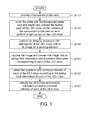
- FIG. 1 shows a flowchart of a detection method for wafer level LED chips according to an embodiment of the disclosure.
- FIG. 2 shows a detection device for wafer level LED chips according to an embodiment of the disclosure.
- FIG. 3A shows a top view of a transparent probe card according to an embodiment of the disclosure.
- FIG. 3B shows a top view of LED chips disposed on a base substrate
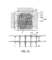
- FIG. 3C shows a top view of a transparent probe card disposed on a wafer and a partial enlargement of region A;
- FIG. 4 shows a flowchart of light filtering process according to a preferred embodiment of the disclosure.
- FIG. 5 shows an image processing module according to an embodiment of the disclosure.
- a detection method and detection device for wafer level LED chips and a transparent probe card thereof disclosed in an embodiment of the disclosure mainly perform electric property analysis and light-up test on the LED chips disposed on a base substrate.
- a transparent probe card combined with an image processing module are used as an electrical detection unit and an optical detection unit for the LED chips, and the LED chips are classified according to the obtained information of spectrums and luminous intensities.
- the detection method includes steps S110 ⁇ S160.
- step S110 a transparent probe card is provided.
- step S120 A wafer is covered with the transparent probe card, and the testing pads of each of the LED chips are electrically connected via the contacts of the transparent probe card so as to perform a light-up test on the LED chips.
- step S130 an imaging process is performed on the light signals of the LED chips to form an image on a sensing element.
- step S140 the image is captured, and the image signal is converted into an optical field information and a position information corresponding to each of the LED chips.
- step S150 the spectrum and luminous intensity of each of the LED chips are obtained according to the optical field information of each of the LED chips.
- step S160 the LED chips are classified according to the spectrum and/or luminous intensity of each of the LED chips.
- the detection method may include a step (not illustrated the diagram) of performing a light filtering process.
- the step of the light filtering process is performed after step S130 of the imaging process, but the disclosure is not limited thereto.
- the step of the filtering process can also be performed before step S130 of the imaging process.
- the detection device includes a transparent probe card 310 (referring to FIG. 3A ), an imaging module 320, an image processing module 330, an analysis module 340 and a classification module 350.
- the transparent probe card 310 covers the wafer 300, and the electrical testing contacts P1 and P2 (illustrated in FIG. 3C ) of the transparent probe card 310 provide power to each of the LED chips 302 disposed on the base substrate 304 so as to perform a light-up test on the LED chips 302.
- the imaging module 320 can be realized by an imaging module 320 composed of a lens 322 or a plurality of lenses 322 for collecting the light signals L and imaging on the image processing module 330, so that the light signals L becomes a recognizable image, such as a spot diagram, wherein the light signal L is formed when the LED chips 302 are lighted up.
- the position (that is, the position information) of the light spot displayed on the spot diagram denotes the actual position of each of the LED chips 302 disposed on the base substrate 304.
- the light spots at different positions contain the information (that is, the optical field information) of the spectrums and the luminous intensities of the LED chips 302 disposed on different positions.
- the image processing module 330 includes an array type charge coupled device (CCD) with high light sensitivity or a sensing element 332 with high resolution level such as a complementary metal oxide semiconductor (CMOS).
- CMOS complementary metal oxide semiconductor
- the image processing module 330 is used for capturing the image, converting the image into an optical field information and a position information corresponding to each of the LED chips 302, and further outputting the optical field information and the corresponding position information to the analysis module 340.
- the analysis module 340 is used for analyzing the optical field information and the corresponding position information of the LED chips.
- the analysis module 340 analyzes the optical field information of each of the LED chips 302 to trace back the spectrum and the luminous intensity of each of the LED chips 302 by the neural image analysis technology.
- the classification module 350 is coupled to the analysis module 340 and the image processing module 330 to obtain the position information of each of the LED chips 302 and perform classification according to the spectrum and the luminous intensity of each of the LED chips 302.
- the classification module 350 includes a display unit (not illustrated) for displaying the positions, distribution, eye-catching colors or marks of the LED chips 302 of different categories which can be used as a basis for classification.
- the detection device further includes a filter module 360 used for filtering the light signals L, which is disposed on the imaging path of the light signals L.
- the filter module 360 is disposed between the imaging module 320 and the image processing module 330, but the disclosure is not limited thereto, and the filter module 360 can also be disposed between the wafer 300 and the imaging module 320.
- FIG. 3A shows a top view of a transparent probe card according to an embodiment of the disclosure.
- FIG. 3B shows a top view of LED chips disposed on a base substrate.
- FIG. 3C shows a top view of a transparent probe card disposed on a wafer and a partial enlargement of region A.
- the transparent probe card 310 includes a transparent substrate 312, a plurality of first transparent conductive wires 314 and a plurality of second transparent conductive wires 316.
- the transparent substrate 312, made from such as glass, covers the wafer 300.
- each of the first transparent conductive wires 314 includes a plurality of first contacts P1 (such as conductive bumps) whose positions respectively corresponding to that of the first testing pads T1 of the LED chips 302.
- first contacts P1 such as conductive bumps
- each of the second transparent conductive wires 316 includes a plurality of second contacts P2 (such as conductive bumps) whose positions respectively corresponding to that of the second testing pads T2 of the LED chips 302.
- first transparent conductive wires 314 and the second transparent conductive wires 316 are separated by such as an insulator (not illustrated), so that the first transparent conductive wires 314 and the second transparent conductive wires 316 are electrically isolated at the junctions.
- first transparent conductive wires 314 and the second transparent conductive wires 316 can also be completely separated by an insulation layer (not illustrated).
- the first transparent conductive wires 314 are disposed on the insulation layer, and the second transparent conductive wires 316 are disposed under the insulation layer electrically connected to the second contacts P2 via a plurality of conductive vias (not illustrated) passing through the insulation layer, wherein the second contacts P2 are disposed on the insulation layer and corresponding to the conductive vias,.
- the transparent probe card 310 covers the wafer 300, and has a size slightly larger than or equal to that of the wafer 300.
- the first testing pads T1 (such as P-type electrodes) and the second testing pads T2 (such as N-type electrodes) disposed on each of the LED chips 302 are electrically connected via the first contacts P1 and the second contacts P2 disposed on the first transparent conductive wires 314 and the second transparent conductive wires 316 respectively.
- the first testing pads T1 are used for receiving a first voltage (such as a positive voltage), and the second testing pads T2 are used for receiving a second voltage (such as a negative voltage, a ground voltage, or other voltages lower than the first voltage).
- the transparent probe card 310 electrifies the first testing pads T1 and the second testing pads T2 of each of the LED chips 302, the luminous layer of each of the LED chips 302 is powered on and illuminates so that a light-up test can be performed on the LED chips 302 disposed on the base substrate 304. Since the substrate and the conductive wires of the transparent probe card 310 are both made from transparent material, the transparent probe card 310, despite covering on the wafer 300, will not block the light signal L emitted from the LED chips 302, and the subsequent process of capturing the image formed by the light signal L emitted from the LED chips 302 will not be affected either.
- a part or a totality of the first transparent conductive layer 314 and the second transparent conductive layer 316 disposed on the transparent probe card 310 can be selectively electrified, so that one or several rows of LED chips 302, and a part or a totality of the LED chips 302 distributed on the base substrate 304 can be sequentially or regionally powered to perform electric property test and light-up test via circuit control.
- the LED chips 302 can be sequentially lighted up in a top down manner, meanwhile, the image of the LED chips 302 on the same row can be captured so as to obtain the optical field information and position information of each of the LED chips 302 on the same row.
- the voltage-current supplied by the contacts P1 and P2 disposed on the transparent probe card 310 to perform electric property test can be controlled by an external auto testing equipment (ATE) to obtain the luminous intensity of each of the LED chips 302 and a voltage-current optical-electro characteristics curve.
- ATE external auto testing equipment
- the values of the electric test (such as the working voltage and the reverse breakdown voltage) transmitted to the auto testing equipment via the test contacts P1 and P2 of the transparent probe card 310 can also be stored in the auto testing equipment and used as a basis for classifying the LED chips 302.
- FIG. 4 shows a flowchart of light filtering process according to an embodiment of the disclosure.
- a rotary disk 362 is provided, wherein a first filter F1, a second filter F2 and a third filter F3 are respectively disposed on the peripheral region of the rotary disk 362, and rotate around of the center of the rotary disk 362 and change their positions accordingly.
- the rotary disk 362 is rotated for enabling the first filter F1 to be disposed on the optical path of the light signal L of the LED chips 302 to form a first sub-image on the sensing element 332.
- the first filter F1 such as a red light filter
- the first filter F1 can filter off the light of all range of wavelengths except the red light wavelength, so that the first sub-image only corresponds to the red light component of the light signal L.
- the rotary disk 362 is again rotated for enabling the second filter F2 to be disposed on the optical path of the light signals L of the LED chips 302 to form a second sub-image on the sensing element 332.
- the second filter F2 such as a green light filter, can filter off the light of all range of wavelengths except the green light wavelength, so that the second sub-image only corresponds to the green light component of the light signal L.
- the rotary disk 362 is again rotated for enabling the third filter F3 to be disposed on the optical path of the light signals L of the LED chips 302 to form a third sub-image on the sensing element 332.
- the third filter F3 such as a blue light filter, can filter off the light of all range of wavelengths except the blue light wavelength, so that the third sub-image only corresponds to the blue light component of the light signal L.
- the image processing module 330 such as a high-end computing image processor, includes a first processing unit 333, a second processing unit 334, a third processing unit 335 and a merging unit 336.
- the merging unit 336 is electrically connected to the first processing unit 333, the second processing unit 334 and the third processing unit 335.
- the first processing unit 333 is used for processing the first sub-image and converting the signal of the first sub-image into a first color light information corresponding to each of the LED chips 302.
- the first color light information includes such as the information of the spectrum and luminous intensity of the red light.
- the second processing unit 334 is used for processing the second sub-image and converting the signal of the second sub-image into a second color light information corresponding to each of the LED chips 302.
- the second color light information includes such as the information of the spectrum and luminous intensity of the green light.
- the third processing unit 335 is used for processing the third sub-image and converting the signal of the third sub-image into a third color light information corresponding to each of the LED chips 302.
- the third color light information includes such as the information of the spectrum and luminous intensity of the blue light.
- the merging unit 336 is used for merging the first, the second and the third color light information to reproduce the optical field information corresponding to all of the spectrums of the visible lights and the luminous intensities of the visible lights of each of the LED chips 302.
- the LED chips disposed on the base substrate are lighted up by the transparent probe card, and a light-up test is performed on a part or all of the LED chips.
- the imaging process is performed by the imaging module and the image processing module for one or several times, so that all of the optical field information and position information of the LED chips can be obtained at one time.
- the conventional point testing device can only detect one single LED chip at a time. Afterwards, the spectrum and luminous intensity of each of the LED chips are obtained by the analysis module for performing classification.
- the detection method and detection device for wafer level LED chips and the transparent probe card thereof disclosed in the disclosure not only meet the market requirements of fast response rate, excellent reproducibility, high light sensitivity and simple detection system, but also have the advantages of quick detection and classification.
Landscapes
- Physics & Mathematics (AREA)
- General Physics & Mathematics (AREA)
- Chemical & Material Sciences (AREA)
- Analytical Chemistry (AREA)
- Biochemistry (AREA)
- Life Sciences & Earth Sciences (AREA)
- Health & Medical Sciences (AREA)
- General Health & Medical Sciences (AREA)
- Immunology (AREA)
- Pathology (AREA)
- Optics & Photonics (AREA)
- Testing Or Measuring Of Semiconductors Or The Like (AREA)
- Testing Of Individual Semiconductor Devices (AREA)
- Led Devices (AREA)
Abstract
Description
- This application claims the benefit of Taiwan application Serial No.
99134642, filed October 11, 2010 - The disclosure relates in general to a chip detection method, a detection device and a probe card thereof, and more particularly to a detection method and a detection device for wafer level light emitting diode (LED) chips, and a transparent probe card thereof.
- The conventional detection method for test of the luminescent properties of the LED chips on the wafer one by one is performed with a point testing device. Suppose there are 2000 LED chips on a 2-inch wafer, the testing time is tedious and efficiency is poor when the LED chips are tested one by one by the point testing method.
- Examples of the conventional point testing device include the point testing structure disclosed in the Taiwanese Patent Publication No.
M382577 M260860 - The disclosure is directed to a detection method and a detection device for wafer level LED chips and a transparent probe card thereof. The detection method and detection device of the disclosure have the advantages of quick detection and classification. The present disclosure resolves the efficiency problem occurring to the conventional point testing device, which can only detect one single LED chip at a time and is unable to increase the efficiency.
- According to a first aspect of the present disclosure, a detection method for wafer level LED chips is provided. The method is used in a wafer and the wafer includes a base substrate and a plurality of LED chips disposed on a base substrate, wherein each of the LED chips includes at least a testing pad. The detection method includes the following steps. A transparent probe card including a plurality of contacts is provided, wherein the contacts correspond to the testing pads. The transparent probe card covers the wafer for electrically connecting the testing pad via the contacts of the transparent probe card so as to perform a light-up test on the LED chips. When the LED chips are lighted up, an imaging process is performed on the light signals of the LED chips to form an image on a sensing element. The image is captured, and the image is converted into an optical field information and a position information corresponding to each of the LED chips. The spectrum and luminous intensity of each of the LED chips are obtained according to the optical field information of each of the LED chips. The LED chips are classified according to the spectrum and/or luminous intensity of each of the LED chips.
- According to a second aspect of the present disclosure, a detection device for wafer level LED chips is provided. The device is used in a wafer and the wafer includes a base substrate and a plurality of LED chips disposed on a base substrate, wherein each of the LED chips includes at least a testing pad. The detection device includes a transparent probe card, an imaging module, an image processing module, an analysis module and a classification module. The transparent probe card includes a plurality of contacts respectively corresponding to the testing pads. The transparent probe card covers the wafer for electrically connecting the testing pad via the contacts of the transparent probe cards so as to perform a light-up test on the LED chips. The imaging module is used for collecting light signals after lighting up the LED chips to form an image. The image processing module is used for capturing the image and converting the image into an optical field information and a position information corresponding to each of the LED chips. The analysis module is coupled to the image processing module and obtains the spectrum and luminous intensity of each of the LED chips according to each of the optical field information of the LED chips and position information. The classification module couples the analysis module and the image processing module to obtain the position information of each of the LED chips and further classify the LED chips according to the spectrum and/or luminous intensity of each of the LED.
- According to a third aspect of the present disclosure, a transparent probe card used in a wafer is provided. The wafer includes a base substrate and a plurality of LED chips disposed on a base substrate, wherein each of the LED chips includes a plurality of first testing pads and a plurality of second testing pas. The transparent probe card includes a transparent substrate, a plurality of first transparent conductive wires and a plurality of second transparent conductive wires. The first transparent conductive wires are disposed on the transparent substrate, wherein each of the first transparent conductive wires includes a plurality of first contacts whose positions corresponding to that of the first testing pads. The second transparent conductive wires, disposed on the transparent substrate, are intersected and electrically isolated with the first transparent conductive wires, wherein each of the second transparent conductive wires includes a plurality of second contacts whose positions corresponding to that of the second testing pads.
- The above and other aspects of the disclosure will become better understood with regard to the following detailed description of the non-limiting embodiment(s). The following description is made with reference to the accompanying drawings.
-
FIG. 1 shows a flowchart of a detection method for wafer level LED chips according to an embodiment of the disclosure. -
FIG. 2 shows a detection device for wafer level LED chips according to an embodiment of the disclosure. -
FIG. 3A shows a top view of a transparent probe card according to an embodiment of the disclosure. -
FIG. 3B shows a top view of LED chips disposed on a base substrate -
FIG. 3C shows a top view of a transparent probe card disposed on a wafer and a partial enlargement of region A; -
FIG. 4 shows a flowchart of light filtering process according to a preferred embodiment of the disclosure; and -
FIG. 5 shows an image processing module according to an embodiment of the disclosure. - A detection method and detection device for wafer level LED chips and a transparent probe card thereof disclosed in an embodiment of the disclosure mainly perform electric property analysis and light-up test on the LED chips disposed on a base substrate. According to the detection method and device of the embodiment of the disclosure, a transparent probe card combined with an image processing module are used as an electrical detection unit and an optical detection unit for the LED chips, and the LED chips are classified according to the obtained information of spectrums and luminous intensities.
- Referring to
FIG. 1 , a flowchart of a detection method for wafer level LED chips according to an embodiment of the disclosure is shown. The detection method includes steps S110~S160. In step S110, a transparent probe card is provided. In step S120, A wafer is covered with the transparent probe card, and the testing pads of each of the LED chips are electrically connected via the contacts of the transparent probe card so as to perform a light-up test on the LED chips. In step S130, an imaging process is performed on the light signals of the LED chips to form an image on a sensing element. In step S140, the image is captured, and the image signal is converted into an optical field information and a position information corresponding to each of the LED chips. In step S150, the spectrum and luminous intensity of each of the LED chips are obtained according to the optical field information of each of the LED chips. In step S160, the LED chips are classified according to the spectrum and/or luminous intensity of each of the LED chips. - Moreover, prior to step S140 of capturing the image, the detection method may include a step (not illustrated the diagram) of performing a light filtering process. Preferably, the step of the light filtering process is performed after step S130 of the imaging process, but the disclosure is not limited thereto. The step of the filtering process can also be performed before step S130 of the imaging process.
- Referring to
FIG. 2 , a detection device for wafer level LED chips according to an embodiment of the disclosure is shown. The detection device includes a transparent probe card 310 (referring toFIG. 3A ), animaging module 320, animage processing module 330, ananalysis module 340 and aclassification module 350. Thetransparent probe card 310 covers thewafer 300, and the electrical testing contacts P1 and P2 (illustrated inFIG. 3C ) of thetransparent probe card 310 provide power to each of theLED chips 302 disposed on thebase substrate 304 so as to perform a light-up test on the LED chips 302. - Moreover, the
imaging module 320 can be realized by animaging module 320 composed of alens 322 or a plurality oflenses 322 for collecting the light signals L and imaging on theimage processing module 330, so that the light signals L becomes a recognizable image, such as a spot diagram, wherein the light signal L is formed when theLED chips 302 are lighted up. The position (that is, the position information) of the light spot displayed on the spot diagram denotes the actual position of each of theLED chips 302 disposed on thebase substrate 304. The light spots at different positions contain the information (that is, the optical field information) of the spectrums and the luminous intensities of theLED chips 302 disposed on different positions. - The
image processing module 330 includes an array type charge coupled device (CCD) with high light sensitivity or asensing element 332 with high resolution level such as a complementary metal oxide semiconductor (CMOS). Theimage processing module 330 is used for capturing the image, converting the image into an optical field information and a position information corresponding to each of the LED chips 302, and further outputting the optical field information and the corresponding position information to theanalysis module 340. - The
analysis module 340 is used for analyzing the optical field information and the corresponding position information of the LED chips. Theanalysis module 340 analyzes the optical field information of each of theLED chips 302 to trace back the spectrum and the luminous intensity of each of theLED chips 302 by the neural image analysis technology. - The
classification module 350 is coupled to theanalysis module 340 and theimage processing module 330 to obtain the position information of each of theLED chips 302 and perform classification according to the spectrum and the luminous intensity of each of the LED chips 302. In an embodiment, theclassification module 350 includes a display unit (not illustrated) for displaying the positions, distribution, eye-catching colors or marks of theLED chips 302 of different categories which can be used as a basis for classification. - Moreover, the detection device further includes a
filter module 360 used for filtering the light signals L, which is disposed on the imaging path of the light signals L. In an embodiment, thefilter module 360 is disposed between theimaging module 320 and theimage processing module 330, but the disclosure is not limited thereto, and thefilter module 360 can also be disposed between thewafer 300 and theimaging module 320. - Referring to
FIGS. 3A, 3B and3C .FIG. 3A shows a top view of a transparent probe card according to an embodiment of the disclosure.FIG. 3B shows a top view of LED chips disposed on a base substrate.FIG. 3C shows a top view of a transparent probe card disposed on a wafer and a partial enlargement of region A. Thetransparent probe card 310 includes atransparent substrate 312, a plurality of first transparentconductive wires 314 and a plurality of second transparentconductive wires 316. Thetransparent substrate 312, made from such as glass, covers thewafer 300. The first and the second transparentconductive wires transparent substrate 312, and the first transparentconductive wires 314 are intersected and electrically isolated with the second transparentconductive wires 316. As indicated in the partial enlargement ofFIG. 3C , each of the first transparentconductive wires 314 includes a plurality of first contacts P1 (such as conductive bumps) whose positions respectively corresponding to that of the first testing pads T1 of the LED chips 302. In addition, a plurality of second transparentconductive wires 316 are respectively intersected with the first transparentconductive wires 314, and each of the second transparentconductive wires 316 includes a plurality of second contacts P2 (such as conductive bumps) whose positions respectively corresponding to that of the second testing pads T2 of the LED chips 302. - In addition, the junctions between the first transparent
conductive wires 314 and the second transparentconductive wires 316 are separated by such as an insulator (not illustrated), so that the first transparentconductive wires 314 and the second transparentconductive wires 316 are electrically isolated at the junctions. Besides, the first transparentconductive wires 314 and the second transparentconductive wires 316 can also be completely separated by an insulation layer (not illustrated). The first transparentconductive wires 314 are disposed on the insulation layer, and the second transparentconductive wires 316 are disposed under the insulation layer electrically connected to the second contacts P2 via a plurality of conductive vias (not illustrated) passing through the insulation layer, wherein the second contacts P2 are disposed on the insulation layer and corresponding to the conductive vias,. - Referring to
FIG. 2 andFIG. 3C . Thetransparent probe card 310 covers thewafer 300, and has a size slightly larger than or equal to that of thewafer 300. The first testing pads T1 (such as P-type electrodes) and the second testing pads T2 (such as N-type electrodes) disposed on each of theLED chips 302 are electrically connected via the first contacts P1 and the second contacts P2 disposed on the first transparentconductive wires 314 and the second transparentconductive wires 316 respectively. The first testing pads T1 are used for receiving a first voltage (such as a positive voltage), and the second testing pads T2 are used for receiving a second voltage (such as a negative voltage, a ground voltage, or other voltages lower than the first voltage). When thetransparent probe card 310 electrifies the first testing pads T1 and the second testing pads T2 of each of the LED chips 302, the luminous layer of each of the LED chips 302 is powered on and illuminates so that a light-up test can be performed on theLED chips 302 disposed on thebase substrate 304. Since the substrate and the conductive wires of thetransparent probe card 310 are both made from transparent material, thetransparent probe card 310, despite covering on thewafer 300, will not block the light signal L emitted from the LED chips 302, and the subsequent process of capturing the image formed by the light signal L emitted from the LED chips 302 will not be affected either. - In the present embodiment of the disclosure, a part or a totality of the first transparent
conductive layer 314 and the second transparentconductive layer 316 disposed on thetransparent probe card 310 can be selectively electrified, so that one or several rows ofLED chips 302, and a part or a totality of theLED chips 302 distributed on thebase substrate 304 can be sequentially or regionally powered to perform electric property test and light-up test via circuit control. For example, theLED chips 302 can be sequentially lighted up in a top down manner, meanwhile, the image of the LED chips 302 on the same row can be captured so as to obtain the optical field information and position information of each of the LED chips 302 on the same row. - In addition, the voltage-current supplied by the contacts P1 and P2 disposed on the
transparent probe card 310 to perform electric property test can be controlled by an external auto testing equipment (ATE) to obtain the luminous intensity of each of theLED chips 302 and a voltage-current optical-electro characteristics curve. The values of the electric test (such as the working voltage and the reverse breakdown voltage) transmitted to the auto testing equipment via the test contacts P1 and P2 of thetransparent probe card 310 can also be stored in the auto testing equipment and used as a basis for classifying the LED chips 302. - Referring to
FIG. 2 andFIG. 4. FIG. 4 shows a flowchart of light filtering process according to an embodiment of the disclosure. In step S21 0, arotary disk 362 is provided, wherein a first filter F1, a second filter F2 and a third filter F3 are respectively disposed on the peripheral region of therotary disk 362, and rotate around of the center of therotary disk 362 and change their positions accordingly. Next, in steps S220 and S222, therotary disk 362 is rotated for enabling the first filter F1 to be disposed on the optical path of the light signal L of theLED chips 302 to form a first sub-image on thesensing element 332. The first filter F1, such as a red light filter, can filter off the light of all range of wavelengths except the red light wavelength, so that the first sub-image only corresponds to the red light component of the light signal L. Then, in steps S230 and S232, therotary disk 362 is again rotated for enabling the second filter F2 to be disposed on the optical path of the light signals L of theLED chips 302 to form a second sub-image on thesensing element 332. The second filter F2, such as a green light filter, can filter off the light of all range of wavelengths except the green light wavelength, so that the second sub-image only corresponds to the green light component of the light signal L. In steps S240 and S242, therotary disk 362 is again rotated for enabling the third filter F3 to be disposed on the optical path of the light signals L of theLED chips 302 to form a third sub-image on thesensing element 332. The third filter F3, such as a blue light filter, can filter off the light of all range of wavelengths except the blue light wavelength, so that the third sub-image only corresponds to the blue light component of the light signal L. - Referring to
FIG. 5 , an image processing module according to a embodiment of the disclosure is shown. Theimage processing module 330, such as a high-end computing image processor, includes afirst processing unit 333, asecond processing unit 334, athird processing unit 335 and a mergingunit 336. The mergingunit 336 is electrically connected to thefirst processing unit 333, thesecond processing unit 334 and thethird processing unit 335. Thefirst processing unit 333 is used for processing the first sub-image and converting the signal of the first sub-image into a first color light information corresponding to each of the LED chips 302. The first color light information includes such as the information of the spectrum and luminous intensity of the red light. Thesecond processing unit 334 is used for processing the second sub-image and converting the signal of the second sub-image into a second color light information corresponding to each of the LED chips 302. The second color light information includes such as the information of the spectrum and luminous intensity of the green light. Thethird processing unit 335 is used for processing the third sub-image and converting the signal of the third sub-image into a third color light information corresponding to each of the LED chips 302. The third color light information includes such as the information of the spectrum and luminous intensity of the blue light. The mergingunit 336 is used for merging the first, the second and the third color light information to reproduce the optical field information corresponding to all of the spectrums of the visible lights and the luminous intensities of the visible lights of each of the LED chips 302. - According to the detection method and detection device for wafer level LED chips and the transparent probe card thereof disclosed in the above embodiments of the disclosure, the LED chips disposed on the base substrate are lighted up by the transparent probe card, and a light-up test is performed on a part or all of the LED chips. When the LED chips are lighted up, the imaging process is performed by the imaging module and the image processing module for one or several times, so that all of the optical field information and position information of the LED chips can be obtained at one time. The conventional point testing device can only detect one single LED chip at a time. Afterwards, the spectrum and luminous intensity of each of the LED chips are obtained by the analysis module for performing classification. Thus, the detection method and detection device for wafer level LED chips and the transparent probe card thereof disclosed in the disclosure not only meet the market requirements of fast response rate, excellent reproducibility, high light sensitivity and simple detection system, but also have the advantages of quick detection and classification.
- While the disclosure has been described by way of example and in terms of the exemplary embodiment(s), it is to be understood that the disclosure is not limited thereto. On the contrary, it is intended to cover various modifications and similar arrangements and procedures, and the scope of the appended claims therefore should be accorded the broadest interpretation so as to encompass all such modifications and similar arrangements and procedures.
Claims (15)
- A detection method for wafer level LED chips, wherein a wafer comprises a base substrate and a plurality of LED chips disposed on the base substrate, each of the LED chips comprises at least a testing pad, the detection method comprising:providing a transparent probe card comprising a plurality of contacts corresponding to the testing pads;performing an imaging process on light signals of the LED chips when the LED chips are lighted up so to form an image on a sensing element;capturing the image and converting the image into an optical field information and a position information corresponding to each of the LED chips;obtaining a spectrum and luminous intensity of each of the LED chips according to the optical field information of each of the LED chips; andclassifying the LED chips according to the spectrum and/or luminous intensity of each of the LED chips.
- The detection method according to claim 1,wherein the step of providing a transparent probe card further comprising covering the wafer with the transparent probe card and electrically connecting the testing pads via the contacts of the transparent probe card so as to perform a light-up test on the LED chips.
- The detection method according to claim 1, wherein before capturing the image formed by the light signals of the LED chips, the method further comprises performing a light filtering process.
- The detection method according to claim 3, wherein the light filtering process comprises:providing a rotary disk on which a first filter, a second filter and a third filter are disposed;rotating the rotary disk for enabling the first filter to be disposed in an optical path of the light signals of the LED chips to form a first sub-image on the sensing element;rotating the rotary disk for enabling the second filter to be disposed in the optical path of the light signals of the LED chips to form a second sub-image on the sensing element; androtating the rotary disk for enabling the third filter to be disposed in the optical path of the light signals of the LED chips to form a third sub-image on the sensing element.
- The detection method according to claim 4, wherein after the light filtering process, the method further comprises:capturing the first sub-image and converting the first sub-image into a first color light information corresponding to each of the LED chips;capturing the second sub-image and converting the second sub-image into a second color light information corresponding to each of the LED chips;capturing the third sub-image and converting the third sub-image into a third color light information corresponding to each of the LED chips; andmerging the first, the second and the third color light information to obtain the optical field information corresponding to each of the LED chips.
- The detection method according to claim 5 wherein the first color light information comprises information of the spectrum and luminous intensity of a red light, the second color light information comprises information of the spectrum and luminous intensity of a green light, the third color light information comprises information of the spectrum and luminous intensity of a blue light.
- A detection device for wafer level LED chips, wherein the detection device is used in a wafer which comprises a base substrate and a plurality of the LED chips disposed on the base substrate and comprising a plurality of testing pads, the detection device comprises:a transparent probe card comprising a plurality of contacts respectively corresponding to the testing pads and covering on the wafer, wherein the transparent probe card electrically connects the testing pads via the contacts of the transparent probe card so as to perform a light-up test on the LED chips;an imaging module used for collecting light signals after lighting up the LED chips to form an image;an image processing module used for capturing the image and converting the image into an optical field information and a position information corresponding to each of the LED chips;an analysis module coupled to the image processing module, wherein the analysis module obtains a spectrum and luminous intensity of each of the LED chips according to the optical field information and the position information of each of the LED chips; anda classification module used for coupling the analysis module and the image processing module to obtain the position information of each of the LED chips and classifying the LED chips according to the spectrum and/or luminous intensity of each of the LED chips.
- The detection device according to claim 7, further comprising a filter module used for filtering the light signals of the LED chips, wherein the image processing module comprises a sensing element, and the filter module comprises:a rotary disk;a first filter disposed on the rotary disk, wherein the first filter is rotated to an optical path of the light signals of the LED chips along with the rotary disk to form a first sub-image on the sensing element;a second filter disposed on the rotary disk, wherein the second filter is rotated to the optical path of the light signal of the LED chips along with the rotary disk to form a second sub-image on the sensing element; anda third filter disposed on the rotary disk, wherein the third filter is rotated to the optical path of the light signal of the LED chips along with the rotary disk to form a third sub-image on the sensing element.
- The detection device according to claim 8, wherein the image processing module further comprises:a first processing unit used for processing the first sub-image and converting the first sub-image into a first color light information corresponding to each of the LED chips ;a second processing unit used for processing the second sub-image and converting the second sub-image into a second color light information corresponding to each of the LED chips;a third processing unit used for processing the third sub-image and converting the third sub-image into a third color light information corresponding to each of the LED chips; anda merging unit electrically connected to the first, the second and the third processing units for merging the first, the second and the third color light information to reproduce the optical field information corresponding to each of the LED chips.
- The detection method according to claim 9, wherein the first color light information comprises information of the spectrum and luminous intensity of a red light, the second color light information comprises information of the spectrum and luminous intensity of a green light, the third color light information comprises information of the spectrum and luminous intensity of a blue light.
- A transparent probe card used in a wafer according to the detection device of claim 8, wherein the wafer comprises a base substrate and a plurality of the LED chips disposed on the base substrate, wherein each of the LED chips comprises a plurality of first testing pads and a plurality of second testing pads, the transparent probe card comprising:a transparent substrate;a plurality of first transparent conductive wires disposed on the transparent substrate, wherein each of the first transparent conductive wires comprises a plurality of first contacts whose positions corresponding to that of the first testing pads; anda plurality of second transparent conductive wires disposed on the transparent substrate and intersected and electrically isolated with the first transparent conductive wires, wherein each of the second transparent conductive wires comprises a plurality of second contacts whose positions corresponding to that of the second testing pads.
- The transparent probe card according to claim 11, wherein a material of the transparent substrate comprises glass, and a material of the first and the second transparent conductive wires comprises indium tin oxide.
- The transparent probe card according to claim 11, wherein the first and the second contacts are conductive bumps.
- The transparent probe card according to claim 11, wherein the first transparent conductive wires and the second transparent conductive wires are substantially perpendicular to each other and respectively used for receiving a first voltage and a second voltage different from the first voltage.
- The transparent probe card according to claim 11, wherein each of the first testing pads is electrically connected to its corresponding first contact, and each of the second testing pads is electrically connected to its corresponding second contact.
Applications Claiming Priority (1)
| Application Number | Priority Date | Filing Date | Title |
|---|---|---|---|
| TW099134642A TW201216391A (en) | 2010-10-11 | 2010-10-11 | Detection method and detection device for LED chips on wafer and transparent probe card thereof |
Publications (2)
| Publication Number | Publication Date |
|---|---|
| EP2439517A1 true EP2439517A1 (en) | 2012-04-11 |
| EP2439517B1 EP2439517B1 (en) | 2015-04-29 |
Family
ID=44674530
Family Applications (1)
| Application Number | Title | Priority Date | Filing Date |
|---|---|---|---|
| EP20110182130 Not-in-force EP2439517B1 (en) | 2010-10-11 | 2011-09-21 | Detection method and detection device for wafer level led chips and transparent probe card thereof |
Country Status (5)
| Country | Link |
|---|---|
| EP (1) | EP2439517B1 (en) |
| JP (1) | JP2012084883A (en) |
| KR (1) | KR20120037352A (en) |
| CN (1) | CN102445668B (en) |
| TW (1) | TW201216391A (en) |
Cited By (22)
| Publication number | Priority date | Publication date | Assignee | Title |
|---|---|---|---|---|
| US8767198B2 (en) * | 2012-09-27 | 2014-07-01 | Genesis Photonics Inc | Detection apparatus |
| WO2015036368A1 (en) * | 2013-09-10 | 2015-03-19 | Osram Opto Semiconductors Gmbh | Testing device and method for testing optoelectronic components |
| CN104515779A (en) * | 2014-12-21 | 2015-04-15 | 广州市明森机电设备有限公司 | Calibration method and calibration device for concave and convex character codes of smart card |
| DE102017101538A1 (en) | 2017-01-26 | 2018-07-26 | Osram Opto Semiconductors Gmbh | Method for classifying semiconductor chips and semiconductor chip |
| WO2020013441A1 (en) | 2018-07-10 | 2020-01-16 | Samsung Electronics Co., Ltd. | Electronic apparatus, method for manufacturing led module and computer-readable recording medium |
| EP3610275A4 (en) * | 2017-05-29 | 2020-04-29 | Samsung Electronics Co., Ltd. | WAFER PROBE CARD, ANALYSIS APPARATUS COMPRISING SAID CARD AND METHOD FOR MANUFACTURING THE WAFER PROBE CARD |
| US10761146B2 (en) | 2017-05-29 | 2020-09-01 | Samsung Electronics Co., Ltd. | Wafer probe card for evaluating micro light emitting diodes, analysis apparatus including the same, and method of fabricating the wafer probe card |
| CN112033646A (en) * | 2020-08-13 | 2020-12-04 | 歌尔光学科技有限公司 | Multi-lamp module testing method, device and equipment and computer readable storage medium |
| US10962586B2 (en) | 2017-01-23 | 2021-03-30 | Apple Inc. | Light emitting diode (LED) test apparatus and method of manufacture |
| EP3642879A4 (en) * | 2017-06-20 | 2021-04-14 | Tesoro Scientific, Inc. | LUMINESCENT DIODE (LED) TEST APPARATUS AND ASSOCIATED MANUFACTURING PROCESS |
| CN112798923A (en) * | 2019-10-25 | 2021-05-14 | 台湾爱司帝科技股份有限公司 | Light emitting diode wafer and light emitting diode wafer detection device and method |
| US11037841B2 (en) | 2016-12-16 | 2021-06-15 | Apple Inc. | Light emitting diode (LED) test apparatus and method of manufacture |
| CN113791326A (en) * | 2021-09-08 | 2021-12-14 | 严群 | Equipment for realizing photoelectric performance test of LED device by injecting current into dielectric layer |
| CN114252238A (en) * | 2020-09-24 | 2022-03-29 | 均豪精密工业股份有限公司 | Detection equipment and its light-receiving device |
| TWI759864B (en) * | 2020-09-17 | 2022-04-01 | 均豪精密工業股份有限公司 | Detection apparatus and light-receiving device thereof |
| CN114594400A (en) * | 2022-04-11 | 2022-06-07 | 广东中睿智能科技有限公司 | LED module brightness measuring equipment |
| CN116571469A (en) * | 2023-04-07 | 2023-08-11 | 东莞市中麒光电技术有限公司 | Point measurement and sorting method for LED chip packaging body |
| US11788885B2 (en) | 2021-02-26 | 2023-10-17 | Advantest Corporation | Test apparatus, test method, and computer-readable storage medium |
| US11800619B2 (en) | 2021-01-21 | 2023-10-24 | Advantest Corporation | Test apparatus, test method, and computer-readable storage medium |
| US12130324B2 (en) | 2021-01-13 | 2024-10-29 | Advantest Corporation | Test apparatus, test method, and computer-readable storage medium |
| CN119124559A (en) * | 2024-09-23 | 2024-12-13 | 江西耀驰科技有限公司 | A Mini LED chip detection method and device based on a multi-channel probe group |
| US12625176B2 (en) | 2021-09-08 | 2026-05-12 | Advantest Corporation | Testing apparatus, testing method, and computer-readable storage medium |
Families Citing this family (28)
| Publication number | Priority date | Publication date | Assignee | Title |
|---|---|---|---|---|
| DE102012017564B4 (en) * | 2012-09-05 | 2018-10-11 | Universität Konstanz | Device for non-permanent electrical contacting of solar cells for measuring electrical properties |
| GB2508792A (en) | 2012-09-11 | 2014-06-18 | Rec Modules Pte Ltd | Back contact solar cell cell interconnection arrangements |
| TWI467141B (en) * | 2012-12-19 | 2015-01-01 | Ind Tech Res Inst | Measurement device and measurement method |
| CN104101744B (en) * | 2013-04-10 | 2017-05-24 | 佛山市国星半导体技术有限公司 | Probe clamp, and LED rapid lightening testing apparatus and method |
| TWI485371B (en) * | 2013-04-24 | 2015-05-21 | Genesis Photonics Inc | Inspection device |
| KR101408767B1 (en) * | 2013-09-27 | 2014-06-19 | 박지암 | Method for eccentricity measuring of lens type LED module |
| TWI498578B (en) * | 2014-01-29 | 2015-09-01 | King Yuan Electronics Co Ltd | Semiconductor device test system and method for accelerating image processing thereof |
| CN106301218A (en) * | 2016-11-01 | 2017-01-04 | 常州天合光能有限公司 | A kind of test device for many main grids cell piece |
| KR102387464B1 (en) * | 2017-10-12 | 2022-04-15 | 삼성전자주식회사 | Apparatus and method for testing interconnect circuit, and method for manufacturing semiconductor device comprising the method |
| JP2019078685A (en) * | 2017-10-26 | 2019-05-23 | 株式会社ブイ・テクノロジー | Led chip inspection method, inspection device therefor, and led display manufacturing method |
| CN107807321A (en) * | 2017-10-27 | 2018-03-16 | 河海大学常州校区 | A kind of ultraviolet LED Online Transaction Processing |
| KR102430497B1 (en) | 2017-12-07 | 2022-08-08 | 삼성전자주식회사 | Manufacturing method of light emitting device |
| JP7083659B2 (en) * | 2018-02-16 | 2022-06-13 | 株式会社ディスコ | Optical device inspection device and inspection method for optical devices |
| CN109065464A (en) * | 2018-06-25 | 2018-12-21 | 易美芯光(北京)科技有限公司 | A kind of test method of mini LED and micro LED |
| TWI652751B (en) * | 2018-06-26 | 2019-03-01 | 旺矽科技股份有限公司 | Point measuring method for surface-emitting laser crystal grains of vertical resonance cavity |
| CN110967570B (en) * | 2018-09-30 | 2021-11-05 | 上海微电子装备(集团)股份有限公司 | Probe card, automatic optical detection device and method |
| TWI870388B (en) * | 2019-03-02 | 2025-01-21 | 以色列商奧寶科技有限公司 | Micro-luminescent diode luminescence inspection device and optical filter inspection device used in the device and micro-luminescent diode luminescence inspection method using the device incorporated into the process |
| CN110554300B (en) * | 2019-09-05 | 2024-03-29 | 佛山市国星半导体技术有限公司 | Detection device and detection method for detecting hydrolysis resistance of LED chip |
| CN112635339B (en) * | 2019-09-24 | 2023-02-28 | 成都辰显光电有限公司 | Micro-LED test circuit, device and method |
| CN112578307A (en) * | 2019-09-29 | 2021-03-30 | 成都辰显光电有限公司 | Light-emitting device testing device, system and testing method |
| CN112649178A (en) * | 2019-10-12 | 2021-04-13 | 成都辰显光电有限公司 | LED luminescence detection system and LED luminescence detection method |
| CN113324739A (en) * | 2021-06-04 | 2021-08-31 | 盐城东紫光电科技有限公司 | Using method of MiniLED detection equipment with point-to-point multi-optical-path optical component |
| US20220402146A1 (en) * | 2021-06-18 | 2022-12-22 | Win Semiconductors Corp. | Testing system and method of testing and transferring light-emitting element |
| CN114823408B (en) * | 2022-05-05 | 2023-10-24 | 无锡美科微电子技术有限公司 | Wafer inspection system and wafer inspection method |
| WO2024053198A1 (en) * | 2022-09-06 | 2024-03-14 | 株式会社ジャパンディスプレイ | Method for inspecting luminescent elements |
| WO2025003771A1 (en) * | 2023-06-29 | 2025-01-02 | Inziv Ltd. | Fast inspection of device under test |
| TWI874076B (en) * | 2023-12-27 | 2025-02-21 | 麥科先進股份有限公司 | Method for detecting an object, method and equipment for transferring an electronic component, and method for manufacturing a light-emitting diode display |
| TWI890328B (en) * | 2024-02-22 | 2025-07-11 | 友達光電股份有限公司 | Mass detecting apparatus and method for electroluminescent devices array |
Citations (4)
| Publication number | Priority date | Publication date | Assignee | Title |
|---|---|---|---|---|
| DE19717369A1 (en) * | 1996-10-04 | 1998-04-09 | Mitsubishi Electric Corp | Probe card and probe device using such probe card |
| US20060226848A1 (en) * | 2005-03-30 | 2006-10-12 | Youngtek Electronics Corporation | Mass-production LED test device for mass production |
| US20070170933A1 (en) * | 2006-01-23 | 2007-07-26 | Maxmile Technologies, Llc | Method and Apparatus for Nondestructively Evaluating Light-Emitting Materials |
| US20100244055A1 (en) * | 2009-03-24 | 2010-09-30 | Hymite A/S | Semiconductor-based sub-mounts for optoelectronic devices with conductive paths to facilitate testing and binning |
Family Cites Families (9)
| Publication number | Priority date | Publication date | Assignee | Title |
|---|---|---|---|---|
| JPH08306747A (en) * | 1995-04-28 | 1996-11-22 | Matsushita Electric Ind Co Ltd | Semiconductor device inspection method and probe card used for the inspection |
| JP3133938B2 (en) * | 1996-03-08 | 2001-02-13 | シャープ株式会社 | Apparatus for measuring electro-optical characteristics of semiconductor devices |
| CN1184486C (en) * | 2001-12-21 | 2005-01-12 | 瀚宇彩晶股份有限公司 | Electronic product circuit signal location detection system and method |
| JP2006253339A (en) * | 2005-03-10 | 2006-09-21 | Fuji Photo Film Co Ltd | Method and device for measuring radiation angle for light emitting element |
| JP4901246B2 (en) * | 2006-03-15 | 2012-03-21 | 財団法人21あおもり産業総合支援センター | Spectral luminance distribution estimation system and method |
| CN101261306B (en) * | 2008-04-14 | 2010-12-08 | 无锡市易控系统工程有限公司 | Full-automatic wafer test method and equipment accomplishing the method |
| CN101566500A (en) * | 2008-04-23 | 2009-10-28 | 广州市光机电技术研究院 | Device and method for testing LED light source intensity space distribution characteristic |
| JP2010217217A (en) * | 2009-03-13 | 2010-09-30 | Sharp Corp | White color adjusting device of led backlight |
| TWM382577U (en) * | 2009-10-15 | 2010-06-11 | Wecon Automation Corp | Device for spot test |
-
2010
- 2010-10-11 TW TW099134642A patent/TW201216391A/en unknown
- 2010-12-24 CN CN201010621746.6A patent/CN102445668B/en not_active Expired - Fee Related
-
2011
- 2011-09-21 EP EP20110182130 patent/EP2439517B1/en not_active Not-in-force
- 2011-10-07 JP JP2011222652A patent/JP2012084883A/en active Pending
- 2011-10-10 KR KR1020110103079A patent/KR20120037352A/en not_active Ceased
Patent Citations (4)
| Publication number | Priority date | Publication date | Assignee | Title |
|---|---|---|---|---|
| DE19717369A1 (en) * | 1996-10-04 | 1998-04-09 | Mitsubishi Electric Corp | Probe card and probe device using such probe card |
| US20060226848A1 (en) * | 2005-03-30 | 2006-10-12 | Youngtek Electronics Corporation | Mass-production LED test device for mass production |
| US20070170933A1 (en) * | 2006-01-23 | 2007-07-26 | Maxmile Technologies, Llc | Method and Apparatus for Nondestructively Evaluating Light-Emitting Materials |
| US20100244055A1 (en) * | 2009-03-24 | 2010-09-30 | Hymite A/S | Semiconductor-based sub-mounts for optoelectronic devices with conductive paths to facilitate testing and binning |
Cited By (28)
| Publication number | Priority date | Publication date | Assignee | Title |
|---|---|---|---|---|
| TWI460404B (en) * | 2012-09-27 | 2014-11-11 | Genesis Photonics Inc | Detection apparatus |
| US8767198B2 (en) * | 2012-09-27 | 2014-07-01 | Genesis Photonics Inc | Detection apparatus |
| WO2015036368A1 (en) * | 2013-09-10 | 2015-03-19 | Osram Opto Semiconductors Gmbh | Testing device and method for testing optoelectronic components |
| CN104515779A (en) * | 2014-12-21 | 2015-04-15 | 广州市明森机电设备有限公司 | Calibration method and calibration device for concave and convex character codes of smart card |
| US11037841B2 (en) | 2016-12-16 | 2021-06-15 | Apple Inc. | Light emitting diode (LED) test apparatus and method of manufacture |
| US10962586B2 (en) | 2017-01-23 | 2021-03-30 | Apple Inc. | Light emitting diode (LED) test apparatus and method of manufacture |
| DE102017101538A1 (en) | 2017-01-26 | 2018-07-26 | Osram Opto Semiconductors Gmbh | Method for classifying semiconductor chips and semiconductor chip |
| DE102017101538B4 (en) | 2017-01-26 | 2022-09-29 | OSRAM Opto Semiconductors Gesellschaft mit beschränkter Haftung | Process for classifying semiconductor chips |
| US10761146B2 (en) | 2017-05-29 | 2020-09-01 | Samsung Electronics Co., Ltd. | Wafer probe card for evaluating micro light emitting diodes, analysis apparatus including the same, and method of fabricating the wafer probe card |
| EP3610275A4 (en) * | 2017-05-29 | 2020-04-29 | Samsung Electronics Co., Ltd. | WAFER PROBE CARD, ANALYSIS APPARATUS COMPRISING SAID CARD AND METHOD FOR MANUFACTURING THE WAFER PROBE CARD |
| EP3642879A4 (en) * | 2017-06-20 | 2021-04-14 | Tesoro Scientific, Inc. | LUMINESCENT DIODE (LED) TEST APPARATUS AND ASSOCIATED MANUFACTURING PROCESS |
| US10989755B2 (en) | 2017-06-20 | 2021-04-27 | Apple Inc. | Light emitting diode (LED) test apparatus and method of manufacture |
| WO2020013441A1 (en) | 2018-07-10 | 2020-01-16 | Samsung Electronics Co., Ltd. | Electronic apparatus, method for manufacturing led module and computer-readable recording medium |
| EP3803958A4 (en) * | 2018-07-10 | 2021-09-15 | Samsung Electronics Co., Ltd. | ELECTRONIC DEVICE, LED MODULE MANUFACTURING PROCESS AND COMPUTER READABLE RECORDING SUPPORT |
| US11251222B2 (en) | 2018-07-10 | 2022-02-15 | Samsung Electronics Co., Ltd. | Technique of generating a micro light emitting diode module using a plurality of micro LEDs having similar characteristics |
| CN112798923A (en) * | 2019-10-25 | 2021-05-14 | 台湾爱司帝科技股份有限公司 | Light emitting diode wafer and light emitting diode wafer detection device and method |
| CN112033646B (en) * | 2020-08-13 | 2022-09-20 | 歌尔光学科技有限公司 | Multi-lamp module testing method, device and equipment and computer readable storage medium |
| CN112033646A (en) * | 2020-08-13 | 2020-12-04 | 歌尔光学科技有限公司 | Multi-lamp module testing method, device and equipment and computer readable storage medium |
| TWI759864B (en) * | 2020-09-17 | 2022-04-01 | 均豪精密工業股份有限公司 | Detection apparatus and light-receiving device thereof |
| CN114252238A (en) * | 2020-09-24 | 2022-03-29 | 均豪精密工业股份有限公司 | Detection equipment and its light-receiving device |
| US12130324B2 (en) | 2021-01-13 | 2024-10-29 | Advantest Corporation | Test apparatus, test method, and computer-readable storage medium |
| US11800619B2 (en) | 2021-01-21 | 2023-10-24 | Advantest Corporation | Test apparatus, test method, and computer-readable storage medium |
| US11788885B2 (en) | 2021-02-26 | 2023-10-17 | Advantest Corporation | Test apparatus, test method, and computer-readable storage medium |
| CN113791326A (en) * | 2021-09-08 | 2021-12-14 | 严群 | Equipment for realizing photoelectric performance test of LED device by injecting current into dielectric layer |
| US12625176B2 (en) | 2021-09-08 | 2026-05-12 | Advantest Corporation | Testing apparatus, testing method, and computer-readable storage medium |
| CN114594400A (en) * | 2022-04-11 | 2022-06-07 | 广东中睿智能科技有限公司 | LED module brightness measuring equipment |
| CN116571469A (en) * | 2023-04-07 | 2023-08-11 | 东莞市中麒光电技术有限公司 | Point measurement and sorting method for LED chip packaging body |
| CN119124559A (en) * | 2024-09-23 | 2024-12-13 | 江西耀驰科技有限公司 | A Mini LED chip detection method and device based on a multi-channel probe group |
Also Published As
| Publication number | Publication date |
|---|---|
| EP2439517B1 (en) | 2015-04-29 |
| CN102445668A (en) | 2012-05-09 |
| KR20120037352A (en) | 2012-04-19 |
| CN102445668B (en) | 2013-10-16 |
| TW201216391A (en) | 2012-04-16 |
| JP2012084883A (en) | 2012-04-26 |
Similar Documents
| Publication | Publication Date | Title |
|---|---|---|
| EP2439517B1 (en) | Detection method and detection device for wafer level led chips and transparent probe card thereof | |
| US10720468B2 (en) | Redundancy in inorganic light emitting diode displays | |
| US9912291B2 (en) | Method and system for testing indirect bandgap semiconductor devices using luminescence imaging | |
| US9977947B2 (en) | Fingerprint identification method and device thereof | |
| CN109119356B (en) | Detection equipment and detection method of array substrate | |
| JP2011216794A (en) | Light emission measuring apparatus and light emission measuring method, control program, and readable recording medium | |
| US10714667B2 (en) | Method of manufacturing light emitting device | |
| KR20120105828A (en) | Semiconductor light emitting diode chip, method of fabricating the chip and method for quality control of the chip | |
| US11790691B2 (en) | Fingerprint identification sensor, display substrate, display device and fingerprint identification method | |
| CN214225327U (en) | Wafer level light emitting diode chip detection device | |
| US12148786B2 (en) | Electronic detection interface and electronic detection module using the same | |
| US20250321190A1 (en) | Inspection device | |
| CN120870156A (en) | Detection device | |
| US20240008170A1 (en) | Led circuit board structure, led testing and packaging method and led pixel package | |
| TW202135183A (en) | Micro led display panel | |
| TWI485371B (en) | Inspection device | |
| US20230178681A1 (en) | Method for manufacturing display device | |
| CN117218991A (en) | Screen based on luminous detection integrated device and control method and system thereof | |
| JP2024118517A (en) | Solar cell inspection equipment | |
| KR101503142B1 (en) | Apparatus for inspecting a light-emitting device | |
| CN115602661A (en) | A detection device and a detection method for a light-emitting element | |
| US20250374728A1 (en) | Micro-led monitoring |
Legal Events
| Date | Code | Title | Description |
|---|---|---|---|
| AK | Designated contracting states |
Kind code of ref document: A1 Designated state(s): AL AT BE BG CH CY CZ DE DK EE ES FI FR GB GR HR HU IE IS IT LI LT LU LV MC MK MT NL NO PL PT RO RS SE SI SK SM TR |
|
| AX | Request for extension of the european patent |
Extension state: BA ME |
|
| PUAI | Public reference made under article 153(3) epc to a published international application that has entered the european phase |
Free format text: ORIGINAL CODE: 0009012 |
|
| 17P | Request for examination filed |
Effective date: 20120714 |
|
| REG | Reference to a national code |
Ref country code: DE Ref legal event code: R079 Ref document number: 602011016051 Country of ref document: DE Free format text: PREVIOUS MAIN CLASS: G01N0021660000 Ipc: G01N0021956000 |
|
| GRAP | Despatch of communication of intention to grant a patent |
Free format text: ORIGINAL CODE: EPIDOSNIGR1 |
|
| RIC1 | Information provided on ipc code assigned before grant |
Ipc: G01R 31/26 20140101ALI20141017BHEP Ipc: G01N 21/95 20060101ALI20141017BHEP Ipc: G01N 21/956 20060101AFI20141017BHEP |
|
| INTG | Intention to grant announced |
Effective date: 20141119 |
|
| GRAS | Grant fee paid |
Free format text: ORIGINAL CODE: EPIDOSNIGR3 |
|
| GRAA | (expected) grant |
Free format text: ORIGINAL CODE: 0009210 |
|
| AK | Designated contracting states |
Kind code of ref document: B1 Designated state(s): AL AT BE BG CH CY CZ DE DK EE ES FI FR GB GR HR HU IE IS IT LI LT LU LV MC MK MT NL NO PL PT RO RS SE SI SK SM TR |
|
| REG | Reference to a national code |
Ref country code: GB Ref legal event code: FG4D |
|
| REG | Reference to a national code |
Ref country code: CH Ref legal event code: EP |
|
| REG | Reference to a national code |
Ref country code: AT Ref legal event code: REF Ref document number: 724697 Country of ref document: AT Kind code of ref document: T Effective date: 20150515 |
|
| REG | Reference to a national code |
Ref country code: IE Ref legal event code: FG4D |
|
| REG | Reference to a national code |
Ref country code: DE Ref legal event code: R096 Ref document number: 602011016051 Country of ref document: DE Effective date: 20150611 |
|
| REG | Reference to a national code |
Ref country code: AT Ref legal event code: MK05 Ref document number: 724697 Country of ref document: AT Kind code of ref document: T Effective date: 20150429 |
|
| REG | Reference to a national code |
Ref country code: LT Ref legal event code: MG4D |
|
| PG25 | Lapsed in a contracting state [announced via postgrant information from national office to epo] |
Ref country code: PT Free format text: LAPSE BECAUSE OF FAILURE TO SUBMIT A TRANSLATION OF THE DESCRIPTION OR TO PAY THE FEE WITHIN THE PRESCRIBED TIME-LIMIT Effective date: 20150831 Ref country code: NO Free format text: LAPSE BECAUSE OF FAILURE TO SUBMIT A TRANSLATION OF THE DESCRIPTION OR TO PAY THE FEE WITHIN THE PRESCRIBED TIME-LIMIT Effective date: 20150729 Ref country code: FI Free format text: LAPSE BECAUSE OF FAILURE TO SUBMIT A TRANSLATION OF THE DESCRIPTION OR TO PAY THE FEE WITHIN THE PRESCRIBED TIME-LIMIT Effective date: 20150429 Ref country code: ES Free format text: LAPSE BECAUSE OF FAILURE TO SUBMIT A TRANSLATION OF THE DESCRIPTION OR TO PAY THE FEE WITHIN THE PRESCRIBED TIME-LIMIT Effective date: 20150429 Ref country code: LT Free format text: LAPSE BECAUSE OF FAILURE TO SUBMIT A TRANSLATION OF THE DESCRIPTION OR TO PAY THE FEE WITHIN THE PRESCRIBED TIME-LIMIT Effective date: 20150429 Ref country code: HR Free format text: LAPSE BECAUSE OF FAILURE TO SUBMIT A TRANSLATION OF THE DESCRIPTION OR TO PAY THE FEE WITHIN THE PRESCRIBED TIME-LIMIT Effective date: 20150429 |
|
| PG25 | Lapsed in a contracting state [announced via postgrant information from national office to epo] |
Ref country code: LV Free format text: LAPSE BECAUSE OF FAILURE TO SUBMIT A TRANSLATION OF THE DESCRIPTION OR TO PAY THE FEE WITHIN THE PRESCRIBED TIME-LIMIT Effective date: 20150429 Ref country code: RS Free format text: LAPSE BECAUSE OF FAILURE TO SUBMIT A TRANSLATION OF THE DESCRIPTION OR TO PAY THE FEE WITHIN THE PRESCRIBED TIME-LIMIT Effective date: 20150429 Ref country code: IS Free format text: LAPSE BECAUSE OF FAILURE TO SUBMIT A TRANSLATION OF THE DESCRIPTION OR TO PAY THE FEE WITHIN THE PRESCRIBED TIME-LIMIT Effective date: 20150829 Ref country code: AT Free format text: LAPSE BECAUSE OF FAILURE TO SUBMIT A TRANSLATION OF THE DESCRIPTION OR TO PAY THE FEE WITHIN THE PRESCRIBED TIME-LIMIT Effective date: 20150429 Ref country code: GR Free format text: LAPSE BECAUSE OF FAILURE TO SUBMIT A TRANSLATION OF THE DESCRIPTION OR TO PAY THE FEE WITHIN THE PRESCRIBED TIME-LIMIT Effective date: 20150730 |
|
| PG25 | Lapsed in a contracting state [announced via postgrant information from national office to epo] |
Ref country code: DK Free format text: LAPSE BECAUSE OF FAILURE TO SUBMIT A TRANSLATION OF THE DESCRIPTION OR TO PAY THE FEE WITHIN THE PRESCRIBED TIME-LIMIT Effective date: 20150429 Ref country code: EE Free format text: LAPSE BECAUSE OF FAILURE TO SUBMIT A TRANSLATION OF THE DESCRIPTION OR TO PAY THE FEE WITHIN THE PRESCRIBED TIME-LIMIT Effective date: 20150429 |
|
| REG | Reference to a national code |
Ref country code: DE Ref legal event code: R097 Ref document number: 602011016051 Country of ref document: DE |
|
| PG25 | Lapsed in a contracting state [announced via postgrant information from national office to epo] |
Ref country code: SK Free format text: LAPSE BECAUSE OF FAILURE TO SUBMIT A TRANSLATION OF THE DESCRIPTION OR TO PAY THE FEE WITHIN THE PRESCRIBED TIME-LIMIT Effective date: 20150429 Ref country code: CZ Free format text: LAPSE BECAUSE OF FAILURE TO SUBMIT A TRANSLATION OF THE DESCRIPTION OR TO PAY THE FEE WITHIN THE PRESCRIBED TIME-LIMIT Effective date: 20150429 Ref country code: RO Free format text: LAPSE BECAUSE OF NON-PAYMENT OF DUE FEES Effective date: 20150429 Ref country code: PL Free format text: LAPSE BECAUSE OF FAILURE TO SUBMIT A TRANSLATION OF THE DESCRIPTION OR TO PAY THE FEE WITHIN THE PRESCRIBED TIME-LIMIT Effective date: 20150429 |
|
| PLBE | No opposition filed within time limit |
Free format text: ORIGINAL CODE: 0009261 |
|
| STAA | Information on the status of an ep patent application or granted ep patent |
Free format text: STATUS: NO OPPOSITION FILED WITHIN TIME LIMIT |
|
| 26N | No opposition filed |
Effective date: 20160201 |
|
| PG25 | Lapsed in a contracting state [announced via postgrant information from national office to epo] |
Ref country code: LU Free format text: LAPSE BECAUSE OF FAILURE TO SUBMIT A TRANSLATION OF THE DESCRIPTION OR TO PAY THE FEE WITHIN THE PRESCRIBED TIME-LIMIT Effective date: 20150921 Ref country code: IT Free format text: LAPSE BECAUSE OF FAILURE TO SUBMIT A TRANSLATION OF THE DESCRIPTION OR TO PAY THE FEE WITHIN THE PRESCRIBED TIME-LIMIT Effective date: 20150429 Ref country code: MC Free format text: LAPSE BECAUSE OF FAILURE TO SUBMIT A TRANSLATION OF THE DESCRIPTION OR TO PAY THE FEE WITHIN THE PRESCRIBED TIME-LIMIT Effective date: 20150429 |
|
| REG | Reference to a national code |
Ref country code: CH Ref legal event code: PL |
|
| GBPC | Gb: european patent ceased through non-payment of renewal fee |
Effective date: 20150921 |
|
| PG25 | Lapsed in a contracting state [announced via postgrant information from national office to epo] |
Ref country code: SI Free format text: LAPSE BECAUSE OF FAILURE TO SUBMIT A TRANSLATION OF THE DESCRIPTION OR TO PAY THE FEE WITHIN THE PRESCRIBED TIME-LIMIT Effective date: 20150429 |
|
| REG | Reference to a national code |
Ref country code: IE Ref legal event code: MM4A |
|
| REG | Reference to a national code |
Ref country code: FR Ref legal event code: ST Effective date: 20160531 |
|
| PG25 | Lapsed in a contracting state [announced via postgrant information from national office to epo] |
Ref country code: GB Free format text: LAPSE BECAUSE OF NON-PAYMENT OF DUE FEES Effective date: 20150921 Ref country code: LI Free format text: LAPSE BECAUSE OF NON-PAYMENT OF DUE FEES Effective date: 20150930 Ref country code: CH Free format text: LAPSE BECAUSE OF NON-PAYMENT OF DUE FEES Effective date: 20150930 Ref country code: IE Free format text: LAPSE BECAUSE OF NON-PAYMENT OF DUE FEES Effective date: 20150921 |
|
| PG25 | Lapsed in a contracting state [announced via postgrant information from national office to epo] |
Ref country code: BE Free format text: LAPSE BECAUSE OF FAILURE TO SUBMIT A TRANSLATION OF THE DESCRIPTION OR TO PAY THE FEE WITHIN THE PRESCRIBED TIME-LIMIT Effective date: 20150429 Ref country code: FR Free format text: LAPSE BECAUSE OF NON-PAYMENT OF DUE FEES Effective date: 20150930 |
|
| PG25 | Lapsed in a contracting state [announced via postgrant information from national office to epo] |
Ref country code: MT Free format text: LAPSE BECAUSE OF FAILURE TO SUBMIT A TRANSLATION OF THE DESCRIPTION OR TO PAY THE FEE WITHIN THE PRESCRIBED TIME-LIMIT Effective date: 20150429 |
|
| PG25 | Lapsed in a contracting state [announced via postgrant information from national office to epo] |
Ref country code: BG Free format text: LAPSE BECAUSE OF FAILURE TO SUBMIT A TRANSLATION OF THE DESCRIPTION OR TO PAY THE FEE WITHIN THE PRESCRIBED TIME-LIMIT Effective date: 20150429 Ref country code: SM Free format text: LAPSE BECAUSE OF FAILURE TO SUBMIT A TRANSLATION OF THE DESCRIPTION OR TO PAY THE FEE WITHIN THE PRESCRIBED TIME-LIMIT Effective date: 20150429 Ref country code: HU Free format text: LAPSE BECAUSE OF FAILURE TO SUBMIT A TRANSLATION OF THE DESCRIPTION OR TO PAY THE FEE WITHIN THE PRESCRIBED TIME-LIMIT; INVALID AB INITIO Effective date: 20110921 |
|
| PG25 | Lapsed in a contracting state [announced via postgrant information from national office to epo] |
Ref country code: SE Free format text: LAPSE BECAUSE OF FAILURE TO SUBMIT A TRANSLATION OF THE DESCRIPTION OR TO PAY THE FEE WITHIN THE PRESCRIBED TIME-LIMIT Effective date: 20150429 Ref country code: CY Free format text: LAPSE BECAUSE OF FAILURE TO SUBMIT A TRANSLATION OF THE DESCRIPTION OR TO PAY THE FEE WITHIN THE PRESCRIBED TIME-LIMIT Effective date: 20150429 |
|
| PG25 | Lapsed in a contracting state [announced via postgrant information from national office to epo] |
Ref country code: TR Free format text: LAPSE BECAUSE OF FAILURE TO SUBMIT A TRANSLATION OF THE DESCRIPTION OR TO PAY THE FEE WITHIN THE PRESCRIBED TIME-LIMIT Effective date: 20150429 |
|
| PG25 | Lapsed in a contracting state [announced via postgrant information from national office to epo] |
Ref country code: MK Free format text: LAPSE BECAUSE OF FAILURE TO SUBMIT A TRANSLATION OF THE DESCRIPTION OR TO PAY THE FEE WITHIN THE PRESCRIBED TIME-LIMIT Effective date: 20150429 |
|
| PG25 | Lapsed in a contracting state [announced via postgrant information from national office to epo] |
Ref country code: AL Free format text: LAPSE BECAUSE OF FAILURE TO SUBMIT A TRANSLATION OF THE DESCRIPTION OR TO PAY THE FEE WITHIN THE PRESCRIBED TIME-LIMIT Effective date: 20150429 |
|
| PGFP | Annual fee paid to national office [announced via postgrant information from national office to epo] |
Ref country code: NL Payment date: 20220926 Year of fee payment: 12 Ref country code: DE Payment date: 20220928 Year of fee payment: 12 |
|
| REG | Reference to a national code |
Ref country code: DE Ref legal event code: R119 Ref document number: 602011016051 Country of ref document: DE |
|
| REG | Reference to a national code |
Ref country code: NL Ref legal event code: MM Effective date: 20231001 |
|
| PG25 | Lapsed in a contracting state [announced via postgrant information from national office to epo] |
Ref country code: NL Free format text: LAPSE BECAUSE OF NON-PAYMENT OF DUE FEES Effective date: 20231001 |
|
| PG25 | Lapsed in a contracting state [announced via postgrant information from national office to epo] |
Ref country code: NL Free format text: LAPSE BECAUSE OF NON-PAYMENT OF DUE FEES Effective date: 20231001 |
|
| PG25 | Lapsed in a contracting state [announced via postgrant information from national office to epo] |
Ref country code: DE Free format text: LAPSE BECAUSE OF NON-PAYMENT OF DUE FEES Effective date: 20240403 |