US8767198B2 - Detection apparatus - Google Patents
Detection apparatus Download PDFInfo
- Publication number
- US8767198B2 US8767198B2 US13/838,824 US201313838824A US8767198B2 US 8767198 B2 US8767198 B2 US 8767198B2 US 201313838824 A US201313838824 A US 201313838824A US 8767198 B2 US8767198 B2 US 8767198B2
- Authority
- US
- United States
- Prior art keywords
- light
- emitting diode
- detection apparatus
- sensing device
- concentrating unit
- Prior art date
- Legal status (The legal status is an assumption and is not a legal conclusion. Google has not performed a legal analysis and makes no representation as to the accuracy of the status listed.)
- Active
Links
- 238000001514 detection method Methods 0.000 title claims abstract description 39
- 239000000523 sample Substances 0.000 claims abstract description 30
- 239000000758 substrate Substances 0.000 claims description 10
- 239000000463 material Substances 0.000 claims description 7
- 230000001419 dependent effect Effects 0.000 claims description 5
- 238000002834 transmittance Methods 0.000 claims description 5
- 239000013307 optical fiber Substances 0.000 claims description 4
- 230000002452 interceptive effect Effects 0.000 claims description 3
- 239000002365 multiple layer Substances 0.000 claims description 2
- 239000012141 concentrate Substances 0.000 abstract description 4
- 239000010410 layer Substances 0.000 description 8
- 238000000034 method Methods 0.000 description 5
- 238000012986 modification Methods 0.000 description 4
- 230000004048 modification Effects 0.000 description 4
- VYPSYNLAJGMNEJ-UHFFFAOYSA-N Silicium dioxide Chemical compound O=[Si]=O VYPSYNLAJGMNEJ-UHFFFAOYSA-N 0.000 description 3
- 230000008901 benefit Effects 0.000 description 3
- 238000005229 chemical vapour deposition Methods 0.000 description 2
- 238000000576 coating method Methods 0.000 description 2
- 238000004519 manufacturing process Methods 0.000 description 2
- 239000004793 Polystyrene Substances 0.000 description 1
- 229910052581 Si3N4 Inorganic materials 0.000 description 1
- XUIMIQQOPSSXEZ-UHFFFAOYSA-N Silicon Chemical compound [Si] XUIMIQQOPSSXEZ-UHFFFAOYSA-N 0.000 description 1
- NIXOWILDQLNWCW-UHFFFAOYSA-N acrylic acid group Chemical group C(C=C)(=O)O NIXOWILDQLNWCW-UHFFFAOYSA-N 0.000 description 1
- 238000010420 art technique Methods 0.000 description 1
- 239000011248 coating agent Substances 0.000 description 1
- 230000005611 electricity Effects 0.000 description 1
- 238000009713 electroplating Methods 0.000 description 1
- 238000004049 embossing Methods 0.000 description 1
- 238000005516 engineering process Methods 0.000 description 1
- 238000005530 etching Methods 0.000 description 1
- 230000003203 everyday effect Effects 0.000 description 1
- 238000002347 injection Methods 0.000 description 1
- 239000007924 injection Substances 0.000 description 1
- 230000001788 irregular Effects 0.000 description 1
- 239000003350 kerosene Substances 0.000 description 1
- 239000012528 membrane Substances 0.000 description 1
- QLOAVXSYZAJECW-UHFFFAOYSA-N methane;molecular fluorine Chemical compound C.FF QLOAVXSYZAJECW-UHFFFAOYSA-N 0.000 description 1
- 239000003921 oil Substances 0.000 description 1
- 229920002223 polystyrene Polymers 0.000 description 1
- 230000036632 reaction speed Effects 0.000 description 1
- 229910052710 silicon Inorganic materials 0.000 description 1
- 239000010703 silicon Substances 0.000 description 1
- 235000012239 silicon dioxide Nutrition 0.000 description 1
- 239000000377 silicon dioxide Substances 0.000 description 1
- HQVNEWCFYHHQES-UHFFFAOYSA-N silicon nitride Chemical compound N12[Si]34N5[Si]62N3[Si]51N64 HQVNEWCFYHHQES-UHFFFAOYSA-N 0.000 description 1
- 229910052814 silicon oxide Inorganic materials 0.000 description 1
Images


Classifications
-
- G—PHYSICS
- G01—MEASURING; TESTING
- G01J—MEASUREMENT OF INTENSITY, VELOCITY, SPECTRAL CONTENT, POLARISATION, PHASE OR PULSE CHARACTERISTICS OF INFRARED, VISIBLE OR ULTRAVIOLET LIGHT; COLORIMETRY; RADIATION PYROMETRY
- G01J1/00—Photometry, e.g. photographic exposure meter
- G01J1/42—Photometry, e.g. photographic exposure meter using electric radiation detectors
-
- G—PHYSICS
- G01—MEASURING; TESTING
- G01J—MEASUREMENT OF INTENSITY, VELOCITY, SPECTRAL CONTENT, POLARISATION, PHASE OR PULSE CHARACTERISTICS OF INFRARED, VISIBLE OR ULTRAVIOLET LIGHT; COLORIMETRY; RADIATION PYROMETRY
- G01J1/00—Photometry, e.g. photographic exposure meter
- G01J1/02—Details
- G01J1/04—Optical or mechanical part supplementary adjustable parts
- G01J1/0407—Optical elements not provided otherwise, e.g. manifolds, windows, holograms, gratings
- G01J1/0411—Optical elements not provided otherwise, e.g. manifolds, windows, holograms, gratings using focussing or collimating elements, i.e. lenses or mirrors; Aberration correction
-
- G—PHYSICS
- G01—MEASURING; TESTING
- G01J—MEASUREMENT OF INTENSITY, VELOCITY, SPECTRAL CONTENT, POLARISATION, PHASE OR PULSE CHARACTERISTICS OF INFRARED, VISIBLE OR ULTRAVIOLET LIGHT; COLORIMETRY; RADIATION PYROMETRY
- G01J1/00—Photometry, e.g. photographic exposure meter
- G01J1/02—Details
- G01J1/04—Optical or mechanical part supplementary adjustable parts
- G01J1/0407—Optical elements not provided otherwise, e.g. manifolds, windows, holograms, gratings
- G01J1/0422—Optical elements not provided otherwise, e.g. manifolds, windows, holograms, gratings using light concentrators, collectors or condensers
-
- G—PHYSICS
- G01—MEASURING; TESTING
- G01J—MEASUREMENT OF INTENSITY, VELOCITY, SPECTRAL CONTENT, POLARISATION, PHASE OR PULSE CHARACTERISTICS OF INFRARED, VISIBLE OR ULTRAVIOLET LIGHT; COLORIMETRY; RADIATION PYROMETRY
- G01J1/00—Photometry, e.g. photographic exposure meter
- G01J1/02—Details
- G01J1/04—Optical or mechanical part supplementary adjustable parts
- G01J1/0407—Optical elements not provided otherwise, e.g. manifolds, windows, holograms, gratings
- G01J1/0425—Optical elements not provided otherwise, e.g. manifolds, windows, holograms, gratings using optical fibers
-
- G—PHYSICS
- G01—MEASURING; TESTING
- G01J—MEASUREMENT OF INTENSITY, VELOCITY, SPECTRAL CONTENT, POLARISATION, PHASE OR PULSE CHARACTERISTICS OF INFRARED, VISIBLE OR ULTRAVIOLET LIGHT; COLORIMETRY; RADIATION PYROMETRY
- G01J1/00—Photometry, e.g. photographic exposure meter
- G01J1/42—Photometry, e.g. photographic exposure meter using electric radiation detectors
- G01J1/4257—Photometry, e.g. photographic exposure meter using electric radiation detectors applied to monitoring the characteristics of a beam, e.g. laser beam, headlamp beam
-
- G—PHYSICS
- G02—OPTICS
- G02B—OPTICAL ELEMENTS, SYSTEMS OR APPARATUS
- G02B19/00—Condensers, e.g. light collectors or similar non-imaging optics
- G02B19/0033—Condensers, e.g. light collectors or similar non-imaging optics characterised by the use
- G02B19/0047—Condensers, e.g. light collectors or similar non-imaging optics characterised by the use for use with a light source
- G02B19/0061—Condensers, e.g. light collectors or similar non-imaging optics characterised by the use for use with a light source the light source comprising a LED
- G02B19/0066—Condensers, e.g. light collectors or similar non-imaging optics characterised by the use for use with a light source the light source comprising a LED in the form of an LED array
-
- G—PHYSICS
- G02—OPTICS
- G02B—OPTICAL ELEMENTS, SYSTEMS OR APPARATUS
- G02B19/00—Condensers, e.g. light collectors or similar non-imaging optics
- G02B19/0033—Condensers, e.g. light collectors or similar non-imaging optics characterised by the use
- G02B19/0076—Condensers, e.g. light collectors or similar non-imaging optics characterised by the use for use with a detector
-
- G—PHYSICS
- G01—MEASURING; TESTING
- G01J—MEASUREMENT OF INTENSITY, VELOCITY, SPECTRAL CONTENT, POLARISATION, PHASE OR PULSE CHARACTERISTICS OF INFRARED, VISIBLE OR ULTRAVIOLET LIGHT; COLORIMETRY; RADIATION PYROMETRY
- G01J1/00—Photometry, e.g. photographic exposure meter
- G01J1/42—Photometry, e.g. photographic exposure meter using electric radiation detectors
- G01J2001/4247—Photometry, e.g. photographic exposure meter using electric radiation detectors for testing lamps or other light sources
-
- G—PHYSICS
- G01—MEASURING; TESTING
- G01R—MEASURING ELECTRIC VARIABLES; MEASURING MAGNETIC VARIABLES
- G01R31/00—Arrangements for testing electric properties; Arrangements for locating electric faults; Arrangements for electrical testing characterised by what is being tested not provided for elsewhere
- G01R31/26—Testing of individual semiconductor devices
- G01R31/2607—Circuits therefor
- G01R31/2632—Circuits therefor for testing diodes
- G01R31/2635—Testing light-emitting diodes, laser diodes or photodiodes
Definitions
- the present invention generally relates to a detection apparatus, in particularly a detection apparatus for detecting luminous efficiency of light-emitting diode chips.
- Light-emitting diode emits a monochromatic light by combining different electronic holes to achieve the purposes of lighting or warning. Compared with traditional lighting sources, the light-emitting diode has many benefits including high luminous efficiency, long service life, difficult to break and fast reaction speed, etc. Due to vigorous promotion by governments in recent years and the rapid expansion of LED street lamps in various cities, LEDs used as a method for lighting can been seen everywhere.
- a probe device is used to test the luminous efficiency of the light-emitting diode chips.
- the probe device provides the light-emitting voltage source for the light-emitting diode chips via the probe. Emitted light beams from the light-emitting diode chips pass through a chuck bearing this light-emitting diode chips, then are collected by a light-sensing device of the probe device, and then are used for determining the luminous efficiency of the light-emitting diode chips finally.
- the light beams emitted from the light-emitting diode chips may affect the accuracy of the light-emitting diode chips due to the detecting limit of the light-sensing device.
- one objective of the present invention is to provide a detection apparatus to solve the problem of poor light-collecting efficiency of the light-sensing device.
- Another objective of the present invention is to provide a detection apparatus to collect the emitted light beams from the light-emitting diode chips.
- the other objective of the present invention is to provide a detection apparatus to determine the luminous efficiency of the light-emitting diode chips accurately.
- the present invention provides a detection apparatus comprising a chuck, a probe device, a light-sensing device and a light-concentrating unit.
- the chuck bears light-emitting diode chips
- the probe device comprises two probes and a power supply.
- the two end points of the probes are electrically connected to one of the plurality of light-emitting diode chips and a power supply to make the light-emitting diode chip emit a plurality of the light beams.
- the light-sensing device is disposed on one side of a light-emitting surface of the light-emitting diode chip to receive the light beams emitted from the light-emitting diode chip.
- the light-concentrating unit is disposed between the light-emitting diode chip and the light-sensing device to concentrate the light beams emitted from the light-emitting diode chip.
- the light-concentrating unit and the chuck are interactive, and therefore another one of a plurality of light-emitting diode chips can be detected by moving the chuck.
- the chuck is composed of a material with light transmittance greater than 90%, and the light-sensing device could be an integral sphere, a solar panel, a phototransistor or a light dependent resistance.
- the light-concentrating unit may be a light-concentrating film. More explicitly, the light-concentrating film is a diaphragm with a plurality of micro structures on its surface in order to collect the plurality of light beams passing through the light-concentrating film.
- the light-concentrating unit may be a light-concentrating film.
- the light-concentrating film comprises the substrate with opposite upper and lower surfaces and a plurality of micro structures, and the plurality of micro structures are disposed on a lateral surface of the substrate close to the light-sensing device to collect the plurality of light beams passing through the light-concentrating film.
- the plurality of micro structures are not specifically limited to such following examples only: a plurality of prisms, a plurality of curved bars or a plurality of projections with curved surfaces.
- Said prisms mentioned above comprise the first inclined surface and the second inclined surface, and both of them form a vertex angle.
- Said zenith of the curved bar is an arc shape.
- the light-concentrating unit may be a convergent lens.
- the light-concentrating unit may be a lens assembly.
- the light-concentrating unit may be a light guide element.
- the light guide element comprises a light-incident plane and a light-emitting plane.
- the area of light-emitting plane is smaller than that of the light-incident plane.
- the light-incident plane faces towards the light-emitting diode chips, and the light-emitting plane faces towards the light-sensing device.
- the light-concentrating unit is a light guide element, and the light guide element comprises at least one optical fiber.
- the light-concentrating unit is a multi-layer diaphragm with different refractive indexes.
- the detection apparatus of the present invention has one or several following advantages:
- the detection apparatus of the present invention can solve the problem of poor light-collecting efficiency on the light-sensing device by collecting the emitted light beams from the light-emitting diode chips via the light-concentrating unit.
- the detection apparatus of the present invention can increase the probability of the light beams passing through the light-concentrating unit and arriving at the light-sensing device by guiding the emitted light beams from the light-emitting diode chips via the light guide element.
- the detection apparatus of the present invention can attain the objective of accurately determining the luminous efficiency of the light-emitting diode chips.
- FIG. 1 is a schematic cross-sectional view of a first embodiment of a detection apparatus of the present invention
- FIG. 2 is a schematic cross-sectional view of a second embodiment of the detection apparatus of the present invention.
- FIG. 3A is a schematic cross-sectional view of a first aspect of a light-concentrating unit of the present invention.
- FIG. 3B-3D are schematic cross-sectional views of three examples in a second aspect of the light-concentrating unit of the present invention.
- FIG. 4A is schematic cross-sectional view of a third aspect of the light-concentrating unit of the present invention.
- FIG. 4B is a schematic cross-sectional view of a fourth aspect of the light-concentrating unit of the present invention.
- FIG. 5A is a schematic cross-sectional view of a fifth aspect of the light-concentrating unit of the present invention.
- FIG. 5B is a schematic cross-sectional view of a sixth aspect of the light-concentrating unit of the present invention.
- FIG. 6 is a schematic cross-sectional view of a seventh aspect of the light-concentrating unit of the present invention.
- the detection apparatus of the present invention comprises a chuck 18 , a probe device 100 , a light-sensing device 15 and a light-concentrating unit 20 .
- the chuck 18 bears a plurality of light-emitting chips 10 to be detected
- the probe device 100 comprises two probes 12 and a power supply 13 .
- the two end points of the probes 12 electrically connect to one of the plurality of light-emitting diode chips A and the power supply 13 to make the light-emitting diode chip A emit a plurality of the light beams L 1 .
- the light-sensing device 15 is disposed on one side of a light-emitting surface of the light-emitting diode chip A to receive the light beams L 1 emitted from the light-emitting diode chip.
- the light-concentrating unit 20 is disposed between the light-emitting diode chip A and the light-sensing device 15 to concentrate the light beams L 1 emitted from the light-emitting diode chip A.
- the light-concentrating unit 20 can selectively interact with the chuck 18 .
- the chuck 18 is composed of a material with light transmittance greater than 90%, and the light-sensing device 15 could be a integral sphere, a solar panel, a phototransistor or the light dependent resistance.
- the detection apparatus of the present invention is suitable to be used for determining the luminous efficiency of the light-emitting diode chips 10 .
- the detection process is shown as follows:
- the power supply 13 of probe device 100 provides the voltage source for one of light-emitting diode chips A through the probe 12 , causing the light-emitting diode chip A to emit a plurality of light beams L 1 .
- the plurality of light beams L 1 emitted from the light-emitting diode chip A is incident to the chuck 18 .
- the plurality of light beams L 1 passes through the chuck 18 and is incident to the light-concentrating unit 20 which collects the plurality of light beams L 1 .
- the light-sensing device 15 receives the plurality of light beams L 1 collected by the light-concentrating unit 20 , and the electronic device 17 electrically connected with the light-sensing device 15 shows the luminous efficiency of the light-emitting diode chip A.
- the detection apparatus of the present invention comprises a chuck 18 , a probe device 100 , a light-sensing device 15 and a light-concentrating unit 20 .
- the chuck 18 bears a plurality of light-emitting chips 10 which are waiting to be detected, and the probe device 100 comprises two probes 12 and a power supply 13 .
- the two end points of the probes 12 electrically connect to one of the plurality of light-emitting diode chips A and the power supply 13 to make the light-emitting diode chip A emit a plurality of the light beams L 1 .
- the light-sensing device 15 is disposed on one side of a light-emitting surface of the light-emitting diode chip A to receive the light beams L 1 emitted from the light-emitting diode chip.
- the light-concentrating unit 20 is disposed between the light-emitting diode chip A and the light-sensing device 15 to concentrate the light beams L 1 emitted from the light-emitting diode chip A.
- the light-concentrating unit 20 is selectively interactive with the chuck 18 .
- the light-sensing device 15 could be, for example, an integral sphere, a solar panel, a phototransistor or a light dependent resistance.
- the difference between the first and second embodiments is that, in the second embodiment, the plurality of light beams L 1 emitted from the light-emitting diode chip do not pass through the chuck 18 but directly enter into the light-concentrating unit 20 in order for the light beams L 1 to be collected. Therefore, the chuck 18 in the second embodiment of the present invention is not required to be composed of the material with high light transmittance.
- the detection apparatus of the present invention is suitable to be used for determining the luminous efficiency of the light-emitting diode chips 10 .
- the detection process is as follows.
- the power supply 13 of the probe device 100 provides the voltage source for one of light-emitting diode chips A through the probe 12 , causing the light-emitting diode chip A to emit a plurality of light beams L 1 .
- the plurality of light beams L 1 emitted from the light-emitting diode chip A are incident to the light-concentrating unit 20 .
- the plurality of light beams L 1 are collected by the light-concentrating unit 20 .
- the light-sensing device 15 receives the plurality of light beams L 1 collected by the light-concentrating unit 20 , and the electronic device 17 electrically connected to the light-sensing device 15 shows the luminous efficiency of the light-emitting diode chip A.
- the present invention collects the plurality of light beams emitted from the light-emitting diode chips by utilizing the light-concentrating unit.
- Several aspects of the light-concentrating unit are listed in order to further illustrate the form of the light-concentrating unit, but these aspects are not intended to limit the present invention.
- FIGS. 3A to 5B for schematic cross-sectional views of the first to the sixth embodiments of the light-concentrating unit in accordance with the present invention. While the means of specific embodiments in the present invention has been described, numerous modifications and variations could be made thereto by those skilled in the art without departing from the scope and spirit of the present invention. The modifications and variations should be the scope claimed by the present invention.
- the light-concentrating unit 20 of the present invention may be a light-concentrating film.
- the light-concentrating film is a diaphragm with multiple micro structures 30 on its surface.
- the light-concentrating film is integrally made by such as embossing, or injection, etc.
- the light-concentrating unit 20 of the present invention may be a light-concentrating film.
- the light-concentrating film comprises the substrate 22 with opposite upper and lower surfaces as well as a plurality of micro structures, and the plurality of micro structures are disposed on one lateral surface of the substrate 22 close to the light-sensing device to collect a plurality of light beams passing through the light-concentrating film.
- the micro structures of the second aspect are prisms 32 , curved prisms 33 or projections 34 with curved surfaces.
- said prisms 32 are disposed on a lateral surface of the substrate 22 (upper or lower surface).
- Each prism 32 comprises the first inclined surface P 1 and the second inclined surface P 2 , and both P 1 and P 2 form a vertex angle. Because the objective of the prisms 32 of the second aspect is to collect the light beams entered into the light-concentrating unit 20 . Whatever the angle that can make the prism 32 have vertex angle V 1 with the function of collecting light beams would be within the scope of protection of the present invention.
- said curved prisms 33 are disposed on a lateral surface of the substrate 22 (upper or lower surface) and form the shape of curve on each zenith in order to collect the light beams incident to the light-concentrating unit 20 .
- the projections 34 with curved surface are disposed on one lateral surface of the substrate 22 (upper or lower surface) in order to collect the light beams injected into the light-concentrating unit 20 by its curved surface.
- the arc in both the curved prisms 33 and the projections 34 any curved surface with the function to collect light beams is within the protection range of the present invention.
- the manufacturing method of a micro structure for the second aspect of the light-concentrating unit in accordance with the preferred embodiment of the present invention may comprise the following processes applied for the light-emitting plane of the light-concentrating unit: coating process, dot printing, etching process, laser, chemical vapor deposition (CVD), etc. in order to form a regular or irregular coarse plane on the light-emitting plane of the light-concentrating unit.
- the material of micro structures could be, for example, polystyrene, silicon dioxide, poly acrylic, silicon oxide, silicon nitride, silicon oxynitride or fluorinated carbon.
- the light-concentrating unit 20 of the present invention may be exemplified like the convex lens.
- the light-concentrating unit 20 of the present invention may be exemplified such as a lens assembly.
- the number of transparent mirrors within the lens assembly is not limited to a specific number. As long as it enables the light-concentrating unit collect light beams, it should fall within the scope of protection of the present invention.
- the light-concentrating unit 20 of the present invention is may be light guide element.
- the light guide element comprises a light-incident plane 50 and a light-emitting plane 52 .
- the area of light-emitting plane 52 is smaller than that of light-incident plane 50 .
- the light-incident plane 50 faces towards the light-emitting diode chips, and the light-emitting plane 52 faces towards the light-sensing device.
- surfaces with light-reflecting function are disposed on two sides of the light-concentrating unit 20 of the fifth aspect, and the light-injecting plane 50 is connected with the light-emitting plane 52 via the surface with light-reflecting function. While the light beams injecting into the light-concentrating unit 20 inject on the surface of two sides of said light-concentrating unit, they are reflected back to the inner part of light-concentrating unit 20 by the surface with light-reflecting function. Thus, the light beams are collected further.
- the light-concentrating unit 20 of the present invention may be a light guide element, and the light guide element comprises at least one optical fiber 54 in order to guide a plurality of light beams to enter into the light-concentrating unit 20 .
- the light guide element is not limited to be the optical fiber 54 showed in FIG. 5B .
- any light guide element having the function of guiding light beams is within the scope of protection of the present invention.
- persons skilled in the art are able to realize the type and size of the light-leading device with light guide function, and therefore, it is needless to describe further here.
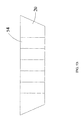
- the light-concentrating unit 20 of the present invention may be a multi-layer diaphragm with different refractive indexes ( FIG. 6 roughly illustrates a two-layer membrane).
- the film layer with high refractive index 60 and that with low refractive index 62 are overlapping.
- the film layer with high refractive index 60 faces towards the light-sensing device to collect the light beams injecting into the light-concentrating unit 20 by increasing the refractive index.
- the production method of the multiple-layer diaphragm may be exemplified by electroplating or coating, etc.
- the light-concentrating unit 20 of the present invention is preferably a multi-layer diaphragm with gradually changing refractive indexes.
- the number of the film layer of the multi-layer diaphragm is not limited to a specific number. As long as it enables the light-concentrating unit to collect light beams, it should fall within the scope of protection of the present invention.
- the detection apparatus of the present invention can collect the emitted light beams from the light-emitting diode chips via the light-concentrating unit, and enhance the efficiency for the collection of light beams on the light-sensing device, and then increasing the accuracy of detection apparatus to determine the luminous efficiency of the light-emitting diode chips.
Abstract
Description
Claims (15)
Applications Claiming Priority (3)
| Application Number | Priority Date | Filing Date | Title |
|---|---|---|---|
| TW101135674A | 2012-09-27 | ||
| TW101135674 | 2012-09-27 | ||
| TW101135674A TWI460404B (en) | 2012-09-27 | 2012-09-27 | Detection apparatus |
Publications (2)
| Publication Number | Publication Date |
|---|---|
| US20140084191A1 US20140084191A1 (en) | 2014-03-27 |
| US8767198B2 true US8767198B2 (en) | 2014-07-01 |
Family
ID=50337954
Family Applications (1)
| Application Number | Title | Priority Date | Filing Date |
|---|---|---|---|
| US13/838,824 Active US8767198B2 (en) | 2012-09-27 | 2013-03-15 | Detection apparatus |
Country Status (2)
| Country | Link |
|---|---|
| US (1) | US8767198B2 (en) |
| TW (1) | TWI460404B (en) |
Cited By (2)
| Publication number | Priority date | Publication date | Assignee | Title |
|---|---|---|---|---|
| US20130015859A1 (en) * | 2011-07-14 | 2013-01-17 | Chroma Ate Inc. | Testing apparatus for light emitting diodes |
| US20160313180A1 (en) * | 2013-12-11 | 2016-10-27 | Infiniled Limited | Apparatus and method for profiling a beam of a light emitting semiconductor device |
Families Citing this family (3)
| Publication number | Priority date | Publication date | Assignee | Title |
|---|---|---|---|---|
| KR20190099004A (en) * | 2016-12-16 | 2019-08-23 | 테소로 사이언티픽, 인코포레이티드 | Light emitting diode test device and manufacturing method |
| CN109917259A (en) * | 2017-12-12 | 2019-06-21 | 宏碁股份有限公司 | Apply the detection system and related detecting method in micromation light emitting device |
| JP7261404B2 (en) * | 2018-06-01 | 2023-04-20 | 株式会社日本マイクロニクス | Manufacturing method of connecting device |
Citations (8)
| Publication number | Priority date | Publication date | Assignee | Title |
|---|---|---|---|---|
| US7064832B2 (en) * | 2003-02-26 | 2006-06-20 | Delaware Capital Formation, Inc. | Color and intensity measuring module for test of light emitting components by automated test equipment |
| US7804589B2 (en) * | 2008-06-13 | 2010-09-28 | Chroma Ate Inc. | System and method for testing light-emitting devices |
| US20100246936A1 (en) * | 2008-06-04 | 2010-09-30 | Won Soo Ji | Led testing apparatus and testing method thereof |
| US20110053295A1 (en) * | 2009-08-28 | 2011-03-03 | Yoon Sang Bok | Resin application apparatus, optical property correction apparatus and method, and method for manufacturing led package |
| EP2439517A1 (en) * | 2010-10-11 | 2012-04-11 | Industrial Technology Research Institute | Detection method and detection device for wafer level led chips and transparent probe card thereof |
| US20120122250A1 (en) * | 2010-11-16 | 2012-05-17 | Samsung Led Co., Ltd. | Apparatus and method for manufacturing led package |
| US20130015859A1 (en) * | 2011-07-14 | 2013-01-17 | Chroma Ate Inc. | Testing apparatus for light emitting diodes |
| US20130301050A1 (en) * | 2012-05-14 | 2013-11-14 | Hon Hai Precision Industry Co., Ltd. | Method and device for testing light-emitting diode die |
-
2012
- 2012-09-27 TW TW101135674A patent/TWI460404B/en not_active IP Right Cessation
-
2013
- 2013-03-15 US US13/838,824 patent/US8767198B2/en active Active
Patent Citations (8)
| Publication number | Priority date | Publication date | Assignee | Title |
|---|---|---|---|---|
| US7064832B2 (en) * | 2003-02-26 | 2006-06-20 | Delaware Capital Formation, Inc. | Color and intensity measuring module for test of light emitting components by automated test equipment |
| US20100246936A1 (en) * | 2008-06-04 | 2010-09-30 | Won Soo Ji | Led testing apparatus and testing method thereof |
| US7804589B2 (en) * | 2008-06-13 | 2010-09-28 | Chroma Ate Inc. | System and method for testing light-emitting devices |
| US20110053295A1 (en) * | 2009-08-28 | 2011-03-03 | Yoon Sang Bok | Resin application apparatus, optical property correction apparatus and method, and method for manufacturing led package |
| EP2439517A1 (en) * | 2010-10-11 | 2012-04-11 | Industrial Technology Research Institute | Detection method and detection device for wafer level led chips and transparent probe card thereof |
| US20120122250A1 (en) * | 2010-11-16 | 2012-05-17 | Samsung Led Co., Ltd. | Apparatus and method for manufacturing led package |
| US20130015859A1 (en) * | 2011-07-14 | 2013-01-17 | Chroma Ate Inc. | Testing apparatus for light emitting diodes |
| US20130301050A1 (en) * | 2012-05-14 | 2013-11-14 | Hon Hai Precision Industry Co., Ltd. | Method and device for testing light-emitting diode die |
Cited By (4)
| Publication number | Priority date | Publication date | Assignee | Title |
|---|---|---|---|---|
| US20130015859A1 (en) * | 2011-07-14 | 2013-01-17 | Chroma Ate Inc. | Testing apparatus for light emitting diodes |
| US9429617B2 (en) * | 2011-07-14 | 2016-08-30 | Chroma Ate Inc. | Testing apparatus for light emitting diodes |
| US20160313180A1 (en) * | 2013-12-11 | 2016-10-27 | Infiniled Limited | Apparatus and method for profiling a beam of a light emitting semiconductor device |
| US11099063B2 (en) * | 2013-12-11 | 2021-08-24 | Facebook Technologies, Llc | Apparatus and method for profiling a beam of a light emitting semiconductor device |
Also Published As
| Publication number | Publication date |
|---|---|
| TWI460404B (en) | 2014-11-11 |
| TW201413224A (en) | 2014-04-01 |
| US20140084191A1 (en) | 2014-03-27 |
Similar Documents
| Publication | Publication Date | Title |
|---|---|---|
| US8767198B2 (en) | Detection apparatus | |
| US9322970B2 (en) | Optical system for coupling light from point light sources into a flat light guide | |
| JP4457100B2 (en) | Lighting device | |
| JP5339707B2 (en) | Linear concentrator | |
| US20100065875A1 (en) | Optical lens and light emitting device using the same | |
| TWI459006B (en) | Detection apparatus for led | |
| US20090213585A1 (en) | Light emitting diode display device | |
| TW200710455A (en) | Optical substrate, manufacturing method thereof, planar lighting device and electrooptical device | |
| JP2010102188A (en) | Light-emitting display board | |
| US9274164B2 (en) | Detection apparatus for light-emitting diode chips having a light sensing device receiving light beams penetrated through a transparent chuck | |
| US20110002126A1 (en) | Lens | |
| WO2007041458A3 (en) | Maximal-aperture reflecting objective | |
| US20120106134A1 (en) | Led ceiling lamp | |
| US7033062B2 (en) | Light source device with optical guiding member and planar light source device employing same | |
| US20150036321A1 (en) | Optical lens and backlight module incorporating the same | |
| TW201610490A (en) | Light guide | |
| TW201326890A (en) | Lens | |
| KR20100108246A (en) | Illumination device | |
| TW201423062A (en) | Detection apparatus for LED | |
| US20100157590A1 (en) | Condensing element systems and methods thereof | |
| CN103728544A (en) | Detection device | |
| US20130100657A1 (en) | Planar illuminating device | |
| US7916404B2 (en) | Fresnel lens with cavities | |
| US20080135093A1 (en) | Optoelectronic Device | |
| TW201405069A (en) | Light source module |
Legal Events
| Date | Code | Title | Description |
|---|---|---|---|
| AS | Assignment |
Owner name: GENESIS PHOTONICS INC, TAIWAN Free format text: ASSIGNMENT OF ASSIGNORS INTEREST;ASSIGNORS:TSAI, TAI-CHENG;WU, TAI-WEI;SHEU, GWO-JIUN;AND OTHERS;REEL/FRAME:030272/0912 Effective date: 20130304 |
|
| STCF | Information on status: patent grant |
Free format text: PATENTED CASE |
|
| MAFP | Maintenance fee payment |
Free format text: PAYMENT OF MAINTENANCE FEE, 4TH YEAR, LARGE ENTITY (ORIGINAL EVENT CODE: M1551) Year of fee payment: 4 |
|
| MAFP | Maintenance fee payment |
Free format text: PAYMENT OF MAINTENANCE FEE, 8TH YEAR, LARGE ENTITY (ORIGINAL EVENT CODE: M1552); ENTITY STATUS OF PATENT OWNER: LARGE ENTITY Year of fee payment: 8 |
|
| AS | Assignment |
Owner name: NICHIA CORPORATION, JAPAN Free format text: ASSIGNMENT OF ASSIGNORS INTEREST;ASSIGNOR:GENESIS PHOTONICS INC.;REEL/FRAME:066044/0807 Effective date: 20231123 Owner name: GENESIS PHOTONICS INC., TAIWAN Free format text: ADDRESS CHANGE REGISTRATION FORM;ASSIGNOR:GENESIS PHOTONICS INC.;REEL/FRAME:066044/0133 Effective date: 20221201 |