EP2417054B1 - Sensor device with reduced error due to parasitic capacitance - Google Patents
Sensor device with reduced error due to parasitic capacitance Download PDFInfo
- Publication number
- EP2417054B1 EP2417054B1 EP10762097.3A EP10762097A EP2417054B1 EP 2417054 B1 EP2417054 B1 EP 2417054B1 EP 10762097 A EP10762097 A EP 10762097A EP 2417054 B1 EP2417054 B1 EP 2417054B1
- Authority
- EP
- European Patent Office
- Prior art keywords
- capacitive
- drive
- node
- parasitic
- sense
- Prior art date
- Legal status (The legal status is an assumption and is not a legal conclusion. Google has not performed a legal analysis and makes no representation as to the accuracy of the status listed.)
- Active
Links
- 230000003071 parasitic effect Effects 0.000 title claims description 123
- 238000012937 correction Methods 0.000 claims description 16
- 238000000034 method Methods 0.000 claims description 14
- 230000004044 response Effects 0.000 claims description 4
- 230000010355 oscillation Effects 0.000 claims description 2
- 239000003990 capacitor Substances 0.000 description 23
- 239000000758 substrate Substances 0.000 description 8
- 230000001133 acceleration Effects 0.000 description 6
- 230000008859 change Effects 0.000 description 6
- 230000003534 oscillatory effect Effects 0.000 description 6
- 238000010586 diagram Methods 0.000 description 5
- 238000004519 manufacturing process Methods 0.000 description 4
- 230000002411 adverse Effects 0.000 description 3
- 238000002372 labelling Methods 0.000 description 3
- 230000009467 reduction Effects 0.000 description 3
- 238000013461 design Methods 0.000 description 2
- 238000001514 detection method Methods 0.000 description 2
- 230000000694 effects Effects 0.000 description 2
- 239000000463 material Substances 0.000 description 2
- 238000004806 packaging method and process Methods 0.000 description 2
- 230000008569 process Effects 0.000 description 2
- 239000004065 semiconductor Substances 0.000 description 2
- 238000013459 approach Methods 0.000 description 1
- 230000001413 cellular effect Effects 0.000 description 1
- 238000004891 communication Methods 0.000 description 1
- 239000004020 conductor Substances 0.000 description 1
- 230000001419 dependent effect Effects 0.000 description 1
- 238000005516 engineering process Methods 0.000 description 1
- 230000010354 integration Effects 0.000 description 1
- 230000003993 interaction Effects 0.000 description 1
- 230000007246 mechanism Effects 0.000 description 1
- 229910044991 metal oxide Inorganic materials 0.000 description 1
- 150000004706 metal oxides Chemical class 0.000 description 1
- 238000012544 monitoring process Methods 0.000 description 1
- 230000010363 phase shift Effects 0.000 description 1
- 238000012545 processing Methods 0.000 description 1
- 238000012552 review Methods 0.000 description 1
- 230000035945 sensitivity Effects 0.000 description 1
- 238000012360 testing method Methods 0.000 description 1
Images


Classifications
-
- G—PHYSICS
- G01—MEASURING; TESTING
- G01C—MEASURING DISTANCES, LEVELS OR BEARINGS; SURVEYING; NAVIGATION; GYROSCOPIC INSTRUMENTS; PHOTOGRAMMETRY OR VIDEOGRAMMETRY
- G01C19/00—Gyroscopes; Turn-sensitive devices using vibrating masses; Turn-sensitive devices without moving masses; Measuring angular rate using gyroscopic effects
- G01C19/56—Turn-sensitive devices using vibrating masses, e.g. vibratory angular rate sensors based on Coriolis forces
- G01C19/5776—Signal processing not specific to any of the devices covered by groups G01C19/5607 - G01C19/5719
-
- B—PERFORMING OPERATIONS; TRANSPORTING
- B81—MICROSTRUCTURAL TECHNOLOGY
- B81B—MICROSTRUCTURAL DEVICES OR SYSTEMS, e.g. MICROMECHANICAL DEVICES
- B81B3/00—Devices comprising flexible or deformable elements, e.g. comprising elastic tongues or membranes
- B81B3/0064—Constitution or structural means for improving or controlling the physical properties of a device
- B81B3/0086—Electrical characteristics, e.g. reducing driving voltage, improving resistance to peak voltage
Definitions
- the present invention relates generally to sensors. More specifically, the present invention relates to a sensor device with reduced parasitic-induced error.
- MEMS Microelectromechanical systems
- MEMS Microelectromechanical systems
- One common application of MEMS is the design and manufacture of sensor devices.
- the electromechanical portion of the device provides the sensing capability, while the electronic portion processes the information obtained by the electromechanical portion.
- One example of a MEMS sensor is a MEMS gyroscope sensor.
- a gyroscope sensor senses angular speed around one or more axes.
- MEMS gyroscope sensor uses a vibrating element to sense angular rate through the detection of a Coriolis force, or acceleration.
- the vibrating element is put into oscillatory motion in the X-axis (drive plane), which is parallel to the substrate. Once the vibrating element is put in motion, it is capable of detecting angular rates induced by the substrate being rotated about the Z-axis.
- the Coriolis acceleration occurs in the Y-axis (sense plane), which is perpendicular to both the X-axis and the Z-axis.
- the Coriolis acceleration produces a motion having an amplitude that is proportional to the angular rotation rate of the substrate.
- parasitic capacitance is the unavoidable and typically unwanted capacitance that exists between the parts of an electronic component or circuit due, in part, to their proximity to one another.
- all actual circuit elements such as, inductors, diodes, and transistors have internal parasitic capacitance, which can cause their behavior to depart from that of "ideal" circuit elements.
- Parasitic capacitance can also exist between closely spaced conductors, such as wires or printed circuit board traces.
- the parasitic capacitance may be inherent in a MEMS sensor or the associated packaging and bonding arrangement, so that the parasitic capacitance values could change not only for different sensor implementations, but the parasitic capacitance values could vary from unit-to-unit in production.
- a MEMS gyroscope sensor has parasitic capacitance between the drive nodes and the sense nodes of the device which produces an error in the signals corresponding to sensor position.
- Parasitic capacitances between the drive nodes and the sense nodes are particularly troublesome, since the parasitic capacitances produce currents that are in quadrature with the desired sensor position signal. Thus, an error is created in the signal determined at the sense nodes so that the position of the vibrating element is determined in error.
- Some approaches involve combining capacitors directly in parallel through a switch in series with each capacitor to create a one-port capacitive network with variable capacitance.
- the minimum capacitance of the switched elements cannot reach zero.
- the minimum achievable capacitance can increase as the number of switched capacitors increases.
- Limitations in the minimum physical size of the capacitors and an increase in the minimum achievable capacitance as the number of switched elements increases are highly undesirable in some MEMS gyroscope sensors where parasitic capacitance values can be in a range of approximately one half to fifty femtofarads.
- JP-A-2002267450 provides a vibration type angular velocity sensor.
- the method of JP-A-2002267450 cancels noise on a monitor/detection signal that results from a drive signal.
- An electromechanical correction is achieved by a weight oscillating in response to the drive signal.
- An electrode can apply a signal in proximity to a driving electrode. The result is the cancellation of the noise that would otherwise affect the output signal from the sensor.
- JP-A2002162228 provides cancellation of noise in another angular velocity sensor. A dummy signal is fed to the sensor to ensure that a noise component is deducted from a detected signal.
- an apparatus comprising the features of appended claim 1 is provided.
- a method comprising the steps of appended claim 12 is provided.
- Embodiments of the invention entail a microelectromechanical (MEMS) sensor with reduced parasitic-induced error and methodology for reducing parasitic-induced error in a MEMS sensor.
- MEMS microelectromechanical
- Two-port capacitive networks are implemented in the MEMS sensor that allow for adjustment of an effective capacitance in order to create opposing currents of the proper phase to cancel parasitic-induced error currents.
- the two-port capacitive networks are adjustable over a wide range of capacitances and allow the effective capacitances to be made as small as needed (e.g., below the smallest on-chip components or parasitic capacitances).
- the MEMS sensor discussed below is an inertial sensor having the appropriate circuitry and structure to form a MEMS gyroscope sensor with reduced parasitic-induced error.
- the principles discussed below that yield reduced parasitic-induced error may alternatively be applied to other types of devices, such as MEMS accelerometers, MEMS pressure sensors, and the like.
- the principles can be applied to non-MEMS devices or general integrated circuits. Accordingly, discussion of specific types of inertial sensors, such as a MEMS gyroscope, is exemplary and not intended to limit the scope of various embodiments.
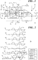
- FIG. 1 shows a schematic diagram of a prior art microelectromechanical systems (MEMS) gyroscope sensor 20 exemplifying the presence of parasitic capacitances 22 and 24.
- MEMS sensor 20 includes a sensor element, such as a resonator element 26, and a sensing circuit 28.
- Resonator element 26 includes one or more movable elements, typically referred to as proof masses. These movable elements are coupled to an underlying substrate (not shown) by various mechanical linkages and springs that enable their movement.
- Various embodiments may include one or more movable elements that may be configured, for example, as drive masses or as sense masses.
- the one or more movable elements are represented by a single structural element, i.e., a single proof mass 30.
- Resonator element 26 includes a drive structure 32 electrically coupled with a pair of drive nodes 34, 36.
- An alternating current (AC) voltage source 38 is coupled between drive nodes 34 and 36.
- Resonator element 26 further includes a sense structure 40 electrically coupled with a pair of sense nodes 42 and 44. Sense nodes 42 and 44 are in electrical communication with a sensing amplifier 46 of sensing circuit 28.
- Drive structure 32 includes moving drive fingers 48 (of which one is shown) extending from proof mass 30 and fixed drive fingers 50 (of which two are shown) which are anchored to an underlying substrate (not shown) so that fixed drive fingers 50 are non-movable relative to moving drive fingers 48.
- moving drive fingers 48 are configured to interleave with pairs of fixed drive fingers 50.
- Sense structure 40 includes moving sense fingers 52 (of which one is shown) extending from proof mass 30 and fixed sense fingers 54 (of which two are shown) which are anchored to the underlying substrate (not shown) so that fixed sense fingers 54 are non-movable relative to moving sense fingers 52.
- moving sense fingers 52 are configured to interleave with pairs of fixed sense fingers 54.
- proof mass 30, drive structure 32, and sense structure 40 are provided for illustrative purposes.
- the size, shape, quantity, and material of proof mass 30, components of drive structure 32, components of sense structure 40, and the like may be selected in accordance with known mechanical design principles to achieve the desired sensitivity, stability, and range of MEMS sensor 20.
- shape, size, material, and spring constants of the mechanical linkage and springs (not shown) suspending proof mass 30 may be selected to achieve the desired movement of proof mass 30.
- MEMS sensor 20 is implemented as a capacitance type gyroscope. That is, a drive signal, e.g., a sinusoidal drive voltage 56, from voltage source 38 is applied between fixed drive fingers 50 due to their electrical connection with drive nodes 34, 36, to cause oscillatory linear motion 58, labeled x(t), of proof mass 30.
- a drive signal e.g., a sinusoidal drive voltage 56
- oscillatory linear motion 58 labeled x(t)
- proof mass 30 will move.
- rotation of MEMS sensor 20 imparts a Coriolis force, also referred to as a Coriolis acceleration, to proof mass 30 that is proportional to the angular velocity, and depends on the orientation of the angular velocity vector with respect to the velocity vector of proof mass 30.
- the Coriolis acceleration, the angular velocity vector, and the mass velocity vector are mutually orthogonal.
- the resulting Coriolis acceleration due to the interaction of oscillatory linear motion 58 applied along the drive axis, i.e. an X-axis 60, and the input angular velocity about, for example, the Z-axis extending out of the page is transmitted along proof mass 30 to moving sense fingers 52.
- each moving sense finger 52 will move along the sense axis, i.e., a Y-axis 62, toward one of the adjacent fixed sense fingers 54 and away from another of the adjacent fixed sense fingers 54.
- the distance that the moving sense finger 52 moves will result in a proportional change in a capacitance 64, labeled C(t), between the fixed sense fingers 52 and the moving sense fingers 54.
- the change in capacitance 64 creates a sense current 66, labeled I(t).
- Sense current 66 is output via sense nodes 42 and 44 to sensing amplifier 46 where it may be amplified and converted to an output voltage 68, labeled V OUT (t), proportional to the angular velocity.
- Parasitic capacitance 22, labeled C P1 is present between drive node 34 and sense node 42, each of which are of the same polarity when drive voltage 56 is applied between drive nodes 34 and 36.
- Parasitic capacitance 22 creates a parasitic current 70, labeled I P1 (t), between drive node 34 and sense node 42.
- parasitic capacitance 24, labeled C P1 is present between drive node 36 and sense node 44, each of which are of the same polarity, when drive voltage 56 is applied between drive nodes 34 and 36.
- Parasitic capacitance 24 creates a parasitic current 72, labeled I P2 (t), between drive node 36 and sense node 44.
- drive node 34 is referred to hereinafter as first drive node 34 and sense node 42 is referred to hereinafter as first sense node 42 to denote their matching polarity.
- drive node 36 is referred to hereinafter as second drive node 36 and sense node 44 is referred to hereinafter as second sense node 44 to denote their matching polarity.
- Parasitic capacitances 22 and 24 are not physical components within MEMS sensor 20. Accordingly, their interconnection with drive nodes 34 and 36 and corresponding sense nodes 42 and 44 are represented by dashed lines.
- Parasitic currents 70 and 72 combine with sense current 66 and are thus output via first and second sense nodes 42 and 44 to sensing amplifier 46. Parasitic currents 70 and 72 may then be amplified with the desired signal, i.e., sense current 66, and converted to output voltage 68 at sensing amplifier 46. Consequently, the resulting output voltage 68 has a parasitic-induced error that adversely affects the sensed angular velocity.
- FIG. 2 shows a chart 74 of waveforms exemplifying parasitic-induced error introduced into the MEMS gyro sensor 20 ( FIG. 1 ) due to parasitic capacitances 22 and 24.
- Chart 74 includes a waveform 76 representing AC drive voltage 56 from voltage source 38 applied at drive nodes 34 and 36.
- Another waveform 78 represents the position, or oscillation, of moving sense fingers 48 extending from proof mass 30 in response to drive voltage 56.
- the next waveform 80 represents time varying capacitance 64 between moving sense fingers 52 and fixed sense fingers 54. Note that waveform 80, representing the time varying capacitance 64, is in phase with waveform 78, representing the position of moving sense fingers 48.
- a next waveform 82 represents sense current 66 related to time varying capacitance 64. Note that waveform 82, representing the changing sense current 66, is in phase with waveform 76, representing drive voltage 56.
- a next waveform 84 represents the combined parasitic currents 70 and 72 resulting from the corresponding parasitic capacitances 22 and 24. Waveform 84, representing the combined parasitic currents 70 and 72, is out of phase with waveform 80 representing sense current 66. Accordingly, a next waveform 86 (solid line) represents output voltage 68 adversely affected by a parasitic-induced error 88.
- Another waveform 90 (dashed line) overlies waveform 86 and represents a desired output voltage 92, labeled V DES (t), without parasitic-induced error 88.
- time varying parasitic capacitances 22 and 24 produce parasitic-induced error 88 in output voltage 68 corresponding to the position of proof mass 30, and consequently to the angular velocity.
- Parasitic capacitance 22 between first drive node 34 and first sense node 42 and parasitic capacitance 24 between second drive node 36 and second sense node 44 cause a phase error at output voltage 68 because the parasitic current contribution, i.e. parasitic currents 70 and 72, is out of phase with sense current 66. Of course, this phase error adversely affects the accuracy of MEMS sensor 20.
- parasitic capacitances 22 and 24 produce currents that are in quadrature with desired output voltage 92.
- a waveform 94 represents a quadrature signal 96 determined at sense nodes 42 and 44 in which parasitic-induced error 88 is also present in quadrature signal 96.
- An embodiment of the invention entails the implementation of two-port capacitive networks that largely cancel parasitic currents 70 and 72 thereby substantially reducing parasitic-induced error 88 on the output voltage 68 and commensurately on quadrature signal 96.
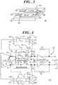
- FIG. 3 shows a perspective view of an exemplary MEMS device 98.
- MEMS device 98 generally includes an electromechanical portion 100 which provides the sensing capability and an electronic portion 102, in the form of a mixed signal integrated circuit (MS IC), which processes the information obtained by electromechanical portion 100.
- MS IC mixed signal integrated circuit
- Both electromechanical portion 100 and electronic portion 102 may be formed on a single substrate 104 with appropriate input and output traces 106 and with appropriate interconnecting traces 108.
- resonator element 26 may be implemented in electromechanical portion 100.
- Sensing circuit 28 FIG. 1
- capacitive networks discussed below
- other circuitry may be implemented in electronic portion 102.
- MEMS device 98 may be used to perform various monitoring and/or control functions in, for example, airbag deployment systems, automatic yaw control devices, safety mechanisms, cellular phones, laptop and notebook computers, cameras, game controllers, and the like where sensor accuracy combined with a miniaturized form factor are required. It should be noted that MEMS device 98 is provided for illustrative purposes. Those skilled in the art will recognize that MEMS device 98 can have various configurations, can have more or less components, and so forth.
- FIG. 4 shows a schematic diagram of a MEMS sensor 110 having two-port capacitive networks 112 and 114 implemented therein for reducing parasitic-induced error 88 ( FIG. 2 ) in accordance with an embodiment of the invention.
- MEMS sensor 110 may be generally configured to form MEMS device 98 ( FIG. 3 ).
- two-port capacitive networks 112 and 114 are discussed in connection with their integration into a MEMS sensor configuration such as that described in connection with FIG. 1 .
- the reference numerals utilized in FIG. 1 are also utilized in FIG. 4 when referencing the same components.
- the specific MEMS sensor can take various structural forms in alternative embodiments.
- MEMS sensor 110 includes resonator element 26 having drive structure 32 electrically coupled with first and second drive nodes 34 and 36, respectively, and sense structure 40 electrically coupled with first and second nodes 42 and 44, respectively.
- parasitic capacitance 22 is present between first drive node 34 and first sense node 42 which creates the phase shifted parasitic current 70 between first drive node 34 and first sense node 42.
- parasitic capacitance 24 is present between second drive node 36 and second sense node 44 which creates the phase shifted parasitic current 72 between second drive node 36 and second sense node 44.
- capacitive networks 112 and 114 may alternatively be applied to other types of MEMS devices, non-MEMS devices, and/or general integrated circuits where a reduction of parasitic-induced error 88 ( FIG. 2 ) is required.
- capacitive network 112 has an input 116 coupled to second drive node 36 and another input 118 coupled to ground.
- capacitive network 112 has an output 120 coupled to first sense node 42 and another output 122 coupled to ground.
- capacitive network 114 has an input 124 coupled to first drive node 34 and another input 126 coupled to ground.
- capacitive network 114 has an output 128 coupled to second sense node 44 and another output 130 coupled to ground.
- a two-port network is an electrical circuit with two pairs of terminals (i.e., the circuit connects two dipoles).
- the two terminals constitute a port if they satisfy a requirement known as a port condition, i.e., the same current must enter and leave a port.
- capacitive network 112 produces an effective capacitance 132, labeled C EFF1 , that is substantially equivalent to parasitic capacitance 22.
- a correction current 134 labeled I C1 (t) is formed through capacitive network 112 that is substantially equivalent to and out of phase with parasitic current 70.
- correction current 134 at sense node 42 cancels parasitic current 70 at sense node 42.
- capacitive network 114 produces an effective capacitance 136, labeled C EFF2 , that is substantially equivalent to parasitic capacitance 24. Accordingly, when drive voltage 56 is applied at input 124, a correction current 138, labeled I C2 (t) is formed through capacitive network 114 that is substantially equivalent to and out of phase with parasitic current 72. Thus, correction current 138 at sense node 44 cancels parasitic current 72 at sense node 44.
- each of capacitive networks 112 and 114 are digitally adjustable over a significant range, for example, over a range of approximately 0.2-50 femtofarads. Such an adjustment range is advantageous in MEMS sensor 110 where each of parasitic capacitances 22 and 24 are likely to be present in the range of 0.5-50 femtofarads. Parasitic capacitances 22 and 24 need not be identical. Accordingly, capacitive networks 112 and 114 are independently adjustable so that they may be individually adjusted, or tuned, to obtain appropriate values of effective capacitances 132 and 136.
- FIG. 5 shows a chart 140 of waveforms exemplifying a reduction in parasitic-induced error 88 ( FIG. 2 ) as a result of implementation of capacitive networks 112 and 114 in MEMS sensor 110.
- chart 140 includes waveform 76 representing AC drive voltage 56 from voltage source 38 applied at drive nodes 34 and 36, and waveform 78 representing oscillatory linear motion 58 of moving sense fingers 48 extending from proof mass 30 in response to drive voltage 56.
- chart 140 includes waveform 80 representing time varying capacitance 64 between moving sense fingers 52 and fixed sense fingers 54 and waveform 82, representing the changing sense current 66.
- Chart 140 further includes a waveform 142 that represents parasitic currents 70 and 72 being substantially canceled by corresponding correction currents 134 and 138. Accordingly, waveform 142 illustrates the total current resulting from parasitic currents 70 and 72 and corresponding correction currents 134 and 138 is substantially zero. Accordingly, a next waveform 144 represents output voltage 68 with parasitic-induced error 88 ( FIG. 2 ) greatly reduced. Likewise, another waveform 148 represents quadrature signal 96 determined at sense nodes 42 and 44 in which parasitic-induced error 88 is greatly reduced. That is, the phase shift from the desired signal, as shown in FIG. 2 , is largely absent in each of waveforms 144 and 148. Consequently, capacitive networks 112 and 114 implemented in MEMS sensor 110 largely cancel parasitic currents 70 and 72 thereby substantially reducing parasitic-induced error 88 on output voltage 68 and commensurately on quadrature signal 96.
- FIG. 6 shows schematic diagram of two-port capacitive network 112 in accordance with an embodiment.
- Capacitive network 112 represents a generalized two-port capacitive network model that, with the appropriate selection of capacitor values and the appropriate selection of capacitor circuits (discussed below), will produce effective capacitance 132 to create correction current 134 that substantially cancels parasitic current 70 ( FIG. 4 ).
- FIG. 6 is discussed in connection with capacitive network 112, it should be understood that the following description applies equivalently to capacitive network 114 ( FIG. 4 ) to yield effective capacitance 136 ( FIG. 4 ) and commensurately correction current 138 ( FIG. 4 ) that substantially cancels parasitic current 72 ( FIG. 4 ).
- Capacitive network 112 includes multiple capacitive circuits 150 connected in parallel. Each of capacitive circuits 150 has a corresponding input 152 coupled to input 116 of capacitive network 112 and a corresponding output 154 coupled to output 120 of capacitive network 112. Each of capacitive circuits 150 produces a circuit capacitance 156, labeled C eff1 , C eff2 , through C eff8 . As is well understood in the art, the total capacitance of two or more capacitors connected in parallel, with the same drive voltage applied to each capacitor, will be the sum of the capacitance values of the individual capacitors connected in parallel.
- effective capacitance 132 i.e., C EFF1
- circuit capacitances 156 i.e., C eff1 , C eff2 , through C eff8 .
- eff circuit capacitances 156
- the lower case labeling nomenclature of "eff" used in connection with circuit capacitances 156 is used herein to differentiate the individual circuit capacitances 156 from the sum of the capacitances, i.e. effective capacitance 132, labeled C EFF1 .
- capacitive network 112 includes eight capacitive circuits 150.
- an eight unit labeling nomenclature of individual components within capacitive circuits 150 is shown (for example, Cn1, Dn2, Cn3, Cn4, Cn5, and Sn, where n is a number between 1 and 8).
- capacitive network 112 is described as having eight capacitive circuits 150, it will become apparent that a capacitive network can be adapted to include more or less than eight capacitive circuits depending upon a desired range of values for effective capacitance 132 and/or the resolution of adjustment steps for capacitive network 112. Only three capacitive circuits 150 are shown in FIG. 6 for simplicity of illustration with ellipses being provided to represent the additional five capacitive circuits 150.
- capacitive circuits 150 are individually controlled by a digital control function 158 of MEMS sensor 110.
- MEMS sensor 110 includes multiple control circuits 162 (each of which are delineated by a dashed-line box), one each of control circuits 162 being coupled to one each of capacitive circuits 150.
- Each of control circuits 162 includes a switch element 164, which in some embodiments, may be a metal oxide semiconductor (MOS) transistor.
- MOS metal oxide semiconductor
- Digital control function 158 includes multiple digital control elements, or logic gates 166.
- digital control function 158 provides eight bits 168 of digital control, with each logic gate 166 providing a single bit 168.
- Each logic gate 166 includes a gate terminal 160 coupled to one of control circuits 162 that functions as a control input to its corresponding control circuit 162. As such, each logic gate 166 provides one bit 168 of digital control to its associated switch element 164.
- the individual logic gates 166 are numbered one through eight, with only three logic gates 166 being shown in association with their respective capacitive circuits 150 for simplicity of illustration. Ellipses are provided to represent the additional five logic gates 166.
- a logic gate performs a logical operation on one or more logic inputs and produces a single logic output, i.e., bit 168, having a first state 170 or a second state 172.
- a logic gate 166 may provide bit 168 in first state 170 that effects closure of (i.e., actuates) the associated switch element 164 or in second state 172 that effects opening of (i.e., de-actuates) the associated switch element 164 of the control circuit 162 to which logic gate 166 is coupled.
- switch element 164 when switch element 164 is closed, a shunt to ground is formed.
- switch element 164 when switch element 164 is closed for a particular capacitive circuit 150, then no current is present at its output, so circuit capacitance 156 is effectively zero.
- switch element 164 when switch element 164 is open, the shunt to ground is removed, and the particular capacitive circuit 150 provides circuit capacitance 156 and therefore a circuit current 174, labeled I eff1 , I eff2 , through I eff8 , at its output 154.
- the sum of the circuit currents 174 yields correction current 134, labeled I C1 (t) at first sense node 42.
- the desired effective capacitance 132 is produced to yield a desired correction current 134 at first sense node 42 that substantially cancels parasitic current 70 ( FIG. 4 ).
- the lower case labeling nomenclature of "eff' used in connection with circuit currents 174 is used herein to correspond with the same nomenclature used for the individual circuit capacitances 156.
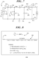
- FIG. 7 shows a circuit model 176 of one of multiple capacitive circuits 150 implemented in either of capacitive networks 112 and 114 ( FIG. 6 ) and FIG. 8 shows a chart 178 corresponding to circuit model 176 that provides equations for determining circuit capacitance 156, C EFF , achievable at each of capacitive circuits 150 in capacitive networks 112 and 114 ( FIG. 4 ).
- Each of capacitive circuits 150 of capacitive networks 112 and 114 is configured as shown in FIG. 7 . However, a combination of differing values of capacitance values within a particular capacitive circuit 150 yields a different circuit capacitance 156 at its output 154.
- Circuit model 176 provides means for determining circuit capacitance 156 for one of capacitive circuits 150.
- parasitic capacitances 22 and 24 ( FIG. 1 ) between drive nodes 34 and 36 and corresponding sense nodes 42 and 44 in a MEMS sensor (e.g., MEMS sensor 20 and MEMS sensor 110) are likely to be present in the range of 0.5 to 50 femtofarads.
- MEMS sensor 20 and MEMS sensor 110 e.g., MEMS sensor 20 and MEMS sensor 110
- parasitic capacitances 22 and 24 may be inherent in the MEMS sensor or the associated packaging and bonding arrangement so that parasitic capacitances 22 and 24 may vary, not only for different sensor implementations, but they may vary from unit-to-unit in production.
- capacitive circuit 150 includes a capacitive element 180, labeled C5, a capacitive element 182, labeled C3, and a capacitive element 184, labeled C1 connected in series.
- Capacitive element 180 has an end 181 coupled to input 152 of capacitive circuit 150 and capacitive element 184 has an end 185 coupled to output 154 of capacitive circuit 150.
- Capacitive circuit 150 further includes a capacitive element 186, labeled C4, and a capacitive element 188, labeled C2.
- Capacitive element 186 has an end 190 between capacitive elements 180 and 182 and another end 192 coupled to ground.
- capacitive element 188 has an end 194 between capacitive elements 182 and 184 and another end 196 coupled to ground.
- capacitive element 180 represents component Cn5 (e.g., C15, C25, through C85) of capacitive circuit 150.
- capacitive element 182 represents component Cn3 (e.g., C13, C23, through C83) of capacitive circuit 150.
- Capacitive element 184 represents component Cn1 (e.g., C11, C21, through C81) of capacitive circuit 150.
- Capacitive element 186 represents component Cn4 (e.g., C14, C24, through C84) of capacitive circuit 150 summed with the switch capacitance C sw across the corresponding switch 164.
- Capacitive element 188 represents component Dn2 (e.g., D12, D22, through D82) of capacitive circuit 150. More particularly, capacitive element 188 represents the capacitance seen at a diode (D12, D22, through D82).
- Capacitive elements 180, 182, 184, 186, and 188 may be integrated circuit (IC) capacitors, parasitic capacitors, or elements that behave substantially as capacitors, such as reverse-biased diodes or open switches.
- sensing amplifier 46 ( FIG. 1 ) maintains a low impedance at output 154, which is less than the impedance of the combination of capacitive elements 180, 182, 184, 186, and 188, then the relationship between drive voltage 56 at input 152 is determined entirely by the impedance of the combination of capacitive elements 180, 182, 184, 186, and 188. This relationship is represented by an equation 198 in chart 178.
- circuit capacitance 156 By analyzing circuit model 176 of capacitive circuit 150 and comparing the relationships, it can be shown that the effective capacitance of capacitive circuit 150, i.e., circuit capacitance 156, can be represented by an equation 200 shown in chart 178. Generally, the values of each of capacitive elements 180, 182, 184, 186, and 188 can be selected according to a predetermined required circuit capacitance 156.
- switch 164 is configured to that capacitive element 186, labeled C4, is shorted when switch 164 is closed. Accordingly, when switch 164 is closed, an effective capacitance at capacitive element 186 is infinite. In such a scenario, circuit capacitance 154 will be zero.
- a switch (not shown) may be arranged in parallel with capacitive element 188.
- an effective capacitance at capacitive element 188 will be infinite, thus producing circuit capacitance 154 of zero.
- FIG. 9 shows a table 202 of exemplary capacitor values for the multiple capacitive elements 180, 182, 184, 186, and 188 within capacitive circuits 150 ( FIG. 6 ) and the resulting effective network capacitances.
- Each row 204 of table 202 provides values for each of capacitive elements 180, 182, 184, 186, and 188 for one of capacitive circuits 150 to obtain a desired circuit capacitance 154.
- Circuit capacitance 154 for each of capacitive circuits 150 is shown in a column 206 of table 202 when an associated one of switch elements 164 ( FIG 6 ) is open, i.e., capacitive circuit 150 is "ON.”
- each row 204 of table 202 also shows that regardless of the values for each of capacitive elements 180, 182, 184, 186, and 188, when an associated one of switch elements 164 is closed, i.e., capacitive circuit 150 is "OFF," circuit capacitance will be zero, represented in a column 208.
- each of effective capacitances 132 and 134 can be determined by summing each of circuit capacitances 154, shown in column 206, for those capacitive circuits 150 that are "ON.”
- the selected values for each of capacitive elements 180, 182, 184, 186, and 188 can result in capacitive circuits 150 having different circuit capacitances 154 with respect to one another.
- the lowest effective capacitance 132 or 134 will be is 0 femtofarads and the highest effective capacitance 132 or 134 will be 51 femtofarads (all circuit capacitances 154 summed).
- capacitive networks 112 and 114 having values for capacitive elements 180, 182, 184, 186, and 188 in accordance with table 202 will yield a wide effective capacitance range (e.g., 0 to 51 femtofarads) with less than one femtofarad resolution (e.g., 0.2, 0.4, and 0.8 femtofarads).
- a terminal impedance 210 labeled Z 11
- a terminal impedance 212 labeled Z 22
- capacitive circuit 150 it is desirable for a terminal impedance 210, labeled Z 11 , at the input and a terminal impedance 212, labeled Z 22 , at the output of capacitive circuit 150 to remain within an acceptable range as capacitive network 112 or 114 is switched.
- neither input 152 nor output 154 should be shorted nor show an excessively large equivalent capacitance, as this could interfere with system operation by excessively loading drive nodes 34 and 36 and/or sense nodes 42 and 44 ( FIG. 4 ).
- excessive loading can create stability problems, can reduce signal levels below desirable levels, and/or can lead to other performance issues.
- terminal impedance 210 ( FIG. 7 ) has been converted to a terminal capacitance 214, labeled C11
- terminal impedance 212 ( FIG. 7 ) has been converted to a terminal capacitance 216, labeled C22.
- a column 218 of values represents terminal capacitance 214 for each combination of capacitive elements 180, 182, 184, 186, and 188 that results in a desired circuit capacitance 154 when an associated one of switch elements 164 ( FIG 6 ) is open, i.e., capacitive circuit 150 is "ON.”
- a column 220 of values represents terminal capacitance 214 when an associated one of switch elements 164 ( FIG 6 ) is closed, i.e., capacitive circuit 150 is "OFF.”
- a column 222 of values represents terminal capacitance 216 when an associated one of switch elements 164 ( FIG 6 ) is open, i.e., capacitive circuit 150 is "ON”
- a column 224 of values represents terminal capacitance 216 when an associated one of switch elements 164 ( FIG 6 ) is closed, i.e., capacitive circuit 150 is "OFF.”
- terminal capacitances 214 and 216 are of similar magnitudes to the values of capacitive elements 180, 182, 184, 186, and 188 so that drive nodes 34 and 36 and/or sense nodes 42 and 44 are not excessively loaded.
- a method for substantially cancelling parasitic currents 70 and 72 ( FIG. 4 ) in a MEMS sensor 110 entails providing capacitor networks 112 and 114 between appropriate drive nodes 34 and 36 and sense nodes 42 and 44, as described in detail above. A determination can then be made of parasitic capacitance 22 between drive node 34 and sense node 42 having the same polarity, and likewise, parasitic capacitance 24 between drive node 36 and sense node 44. This determination can be made in conjunction with post-production testing and calibration of MEMS sensor 110. Each of capacitor networks 112 and 114 can then be separately adjusted via digital control to selectively include, i.e., activate or inactivate, particular capacitive circuits 150 ( FIG. 6 ), as discussed above, to provide respective effective capacitances 132 and 136 ( FIG. 4 ).
- Embodiments of the invention are discussed in connection with two capacitive networks implemented in a differential sensor system.
- a single capacitive network e.g., capacitive network 112 ( FIG. 4 ) may be implemented in a single-ended sensor system.
- an element e.g., a resonator element, may have a single drive node and a single sense node between which parasitic current is present when a drive voltage from a voltage source is applied at the drive node.
- input 116 of capacitive network 112 is coupled to another voltage source and output 120 of capacitive network is coupled to the single sense node.
- the voltage source may be used to apply another drive voltage of opposite phase to capacitive network 112 to produce correction current 134 that substantially cancels the parasitic current.
- Embodiments of the invention entail microelectromechanical systems (MEMS) sensors, such as a gyroscope sensor, with reduced parasitic-induced error and methodology for reducing parasitic-induced error in a MEMS sensor.
- MEMS microelectromechanical systems
- Two-port capacitive networks are implemented in the MEMS sensor that allow for adjustment of an effective capacitance in order to create opposing currents of the proper phase to cancel parasitic-induced error currents.
- the two-port capacitive networks are digitally adjustable over a wide range of capacitances and allow the effective capacitances to be made as small as needed (e.g., below the smallest on-chip components or parasitic capacitances).
- the cancelation of parasitic-induced currents yields improved accuracy of a MEMS sensor.
Landscapes
- Engineering & Computer Science (AREA)
- Radar, Positioning & Navigation (AREA)
- Microelectronics & Electronic Packaging (AREA)
- Signal Processing (AREA)
- Physics & Mathematics (AREA)
- General Physics & Mathematics (AREA)
- Computer Hardware Design (AREA)
- Remote Sensing (AREA)
- Gyroscopes (AREA)
- Micromachines (AREA)
- Networks Using Active Elements (AREA)
- Piezo-Electric Or Mechanical Vibrators, Or Delay Or Filter Circuits (AREA)
- Measuring Fluid Pressure (AREA)
- Pressure Sensors (AREA)
Applications Claiming Priority (2)
| Application Number | Priority Date | Filing Date | Title |
|---|---|---|---|
| US12/421,513 US8096179B2 (en) | 2009-04-09 | 2009-04-09 | Sensor device with reduced parasitic-induced error |
| PCT/US2010/028282 WO2010117615A2 (en) | 2009-04-09 | 2010-03-23 | Sensor device with reduced parasitic-induced error |
Publications (3)
| Publication Number | Publication Date |
|---|---|
| EP2417054A2 EP2417054A2 (en) | 2012-02-15 |
| EP2417054A4 EP2417054A4 (en) | 2015-07-01 |
| EP2417054B1 true EP2417054B1 (en) | 2019-10-02 |
Family
ID=42933902
Family Applications (1)
| Application Number | Title | Priority Date | Filing Date |
|---|---|---|---|
| EP10762097.3A Active EP2417054B1 (en) | 2009-04-09 | 2010-03-23 | Sensor device with reduced error due to parasitic capacitance |
Country Status (6)
| Country | Link |
|---|---|
| US (1) | US8096179B2 (enExample) |
| EP (1) | EP2417054B1 (enExample) |
| JP (1) | JP5557354B2 (enExample) |
| CN (1) | CN102365229B (enExample) |
| TW (1) | TWI502885B (enExample) |
| WO (1) | WO2010117615A2 (enExample) |
Families Citing this family (19)
| Publication number | Priority date | Publication date | Assignee | Title |
|---|---|---|---|---|
| EP2177875A3 (en) * | 2008-10-14 | 2013-04-24 | Watson Industries, Inc. | A Vibrating Structural Gyroscope with Quadrature Control |
| IT1392553B1 (it) * | 2008-12-11 | 2012-03-09 | St Microelectronics Rousset | Dispositivo elettronico a capacita' variabile e dispositivo microelettromeccanico incorporante tale dispositivo elettronico |
| US8714012B2 (en) * | 2010-02-16 | 2014-05-06 | Stmicroelectronics S.R.L. | Microelectromechanical gyroscope with inversion of actuation forces, and method for actuating a microelectromechanical gyroscope |
| ITTO20110688A1 (it) * | 2011-07-28 | 2013-01-29 | St Microelectronics Srl | Giroscopio microelettromeccanico con funzione di autocalibrazione e metodo di calibrazione di un giroscopio microelettromeccanico |
| TWI416070B (zh) | 2011-12-26 | 2013-11-21 | Ind Tech Res Inst | 陀螺儀的讀取電路 |
| US9562767B2 (en) | 2014-08-12 | 2017-02-07 | Honeywell International Inc. | Systems and methods for improving MEMS gyroscope start time |
| JP6413462B2 (ja) | 2014-08-15 | 2018-10-31 | セイコーエプソン株式会社 | 物理量センサー、物理量センサー装置、電子機器および移動体 |
| US10317252B2 (en) | 2015-04-20 | 2019-06-11 | Infineon Technologies Ag | System and method for a capacitive sensor |
| KR101880911B1 (ko) * | 2017-02-21 | 2018-07-23 | 한국기술교육대학교 산학협력단 | 정전 용량형 mems 공진기 |
| CN106993355A (zh) * | 2017-04-06 | 2017-07-28 | 深圳格林绿梵生能源股份有限公司 | 一种基于均衡电容的多路反激led驱动器 |
| FR3079026B1 (fr) * | 2018-03-15 | 2021-01-01 | Sysnav | Procede de calibration d'un gyrometre equipant un vehicule |
| JP7119478B2 (ja) | 2018-03-23 | 2022-08-17 | セイコーエプソン株式会社 | 回路装置、物理量測定装置、電子機器及び移動体 |
| US11820649B2 (en) | 2018-05-18 | 2023-11-21 | Lawrence Livermore National Security, Llc | Position sensing circuit for an electrostatically driven MEMS device |
| US20190352174A1 (en) * | 2018-05-18 | 2019-11-21 | Lawrence Livermore National Security, Llc | Position sensing circuit for an electronically driven mems device |
| US11119606B2 (en) * | 2019-08-20 | 2021-09-14 | Synaptics Incorporated | Background capacitance compensation |
| CN112782427A (zh) * | 2019-11-07 | 2021-05-11 | 霍尼韦尔国际公司 | 用于避免振梁加速度计的电容馈通的谐振器电极配置 |
| FR3108897B1 (fr) * | 2020-04-03 | 2022-04-08 | Commissariat Energie Atomique | Procédé de commande d’un capteur |
| WO2022183030A1 (en) * | 2021-02-26 | 2022-09-01 | Lawrence Livermore National Security, Llc | Position sensing circuit for an electrostatically driven mems device |
| IT202100024644A1 (it) | 2021-09-27 | 2023-03-27 | St Microelectronics Srl | Circuito di controllo di un giroscopio mems, giroscopio mems e metodo di controllo |
Citations (1)
| Publication number | Priority date | Publication date | Assignee | Title |
|---|---|---|---|---|
| US20020175692A1 (en) * | 2001-02-21 | 2002-11-28 | Stmicroelectronics S.R.L. | Method and circuit for detecting movements through micro-electric-mechanical sensors, compensating parasitic capacitances and spurious movements |
Family Cites Families (28)
| Publication number | Priority date | Publication date | Assignee | Title |
|---|---|---|---|---|
| US5175518A (en) * | 1991-10-15 | 1992-12-29 | Watkins-Johnson Company | Wide percentage bandwidth microwave filter network and method of manufacturing same |
| CN1141429A (zh) * | 1995-01-11 | 1997-01-29 | 富川义朗 | 静电型传感器装置中减少电容分量的回路 |
| JP3489390B2 (ja) * | 1997-04-28 | 2004-01-19 | 株式会社村田製作所 | 角速度センサ装置 |
| US6233441B1 (en) * | 1998-05-29 | 2001-05-15 | Silicon Laboratories, Inc. | Method and apparatus for generating a discretely variable capacitance for synthesizing high-frequency signals for wireless communications |
| JP2000081335A (ja) * | 1998-09-07 | 2000-03-21 | Denso Corp | ヨーレートセンサ |
| KR100363783B1 (ko) * | 1999-09-09 | 2002-12-11 | 삼성전기주식회사 | 마이크로 자이로스코프의 각속도출력 보상회로 |
| JP4576703B2 (ja) | 2000-11-27 | 2010-11-10 | 株式会社デンソー | 角速度センサ |
| JP2002267450A (ja) | 2001-03-09 | 2002-09-18 | Denso Corp | 角速度センサ |
| DE10121517A1 (de) * | 2001-05-03 | 2002-11-14 | Infineon Technologies Ag | Verfahren und Vorrichtung zum Einstellen eines aktiven Filters |
| JP3861652B2 (ja) * | 2001-10-16 | 2006-12-20 | 株式会社デンソー | 容量式物理量センサ |
| US6715353B2 (en) * | 2002-04-25 | 2004-04-06 | Honeywell International, Inc. | MEMS gyroscope with parametric gain |
| US7253079B2 (en) * | 2002-05-09 | 2007-08-07 | The Charles Stark Draper Laboratory, Inc. | Coplanar mounting member for a MEM sensor |
| JP3812543B2 (ja) * | 2003-03-28 | 2006-08-23 | 株式会社デンソー | 角速度センサ装置及びその調整方法 |
| ATE452326T1 (de) * | 2004-02-04 | 2010-01-15 | Atlantic Inertial Systems Ltd | Verfahren zur verringerung des vorspannungsfehlers in einem kreisel mit vibrierender struktur |
| JP2005300202A (ja) * | 2004-04-07 | 2005-10-27 | Nippon Soken Inc | 静電振動型角速度センサ |
| US7102365B1 (en) * | 2005-04-01 | 2006-09-05 | Freescale Semiconductor, Inc. | Apparatus for current sensing |
| US7405099B2 (en) * | 2005-07-27 | 2008-07-29 | Freescale Semiconductor, Inc. | Wide and narrow trench formation in high aspect ratio MEMS |
| EP1790988B1 (en) * | 2005-11-29 | 2017-01-18 | STMicroelectronics Srl | Detection circuit using a differential capacitive sensor with input-common-mode control in a sense interface |
| US20070164378A1 (en) * | 2006-01-13 | 2007-07-19 | Honeywell International Inc. | Integrated mems package |
| WO2007135663A1 (en) * | 2006-05-19 | 2007-11-29 | N-Trig Ltd. | Variable capacitor array |
| US7434464B2 (en) * | 2006-09-29 | 2008-10-14 | Freescale Semiconductor, Inc. | Methods and apparatus for a MEMS gyro sensor |
| EP1959234A1 (en) * | 2007-02-13 | 2008-08-20 | STMicroelectronics S.r.l. | Microelectromechanical gyroscope with suppression of capacitive coupling spurious signals and control method of a microelectromechanical gyroscope |
| EP1959562B1 (en) * | 2007-02-15 | 2010-12-08 | STMicroelectronics Srl | Fully differential demodulator with variable gain and method for demodulating a signal |
| CN100439864C (zh) * | 2007-06-01 | 2008-12-03 | 北京沃尔康科技有限责任公司 | 一种新型硅微机械陀螺 |
| US7520170B2 (en) * | 2007-07-10 | 2009-04-21 | Freescale Semiconductor, Inc. | Output correction circuit for three-axis accelerometer |
| US7784344B2 (en) * | 2007-11-29 | 2010-08-31 | Honeywell International Inc. | Integrated MEMS 3D multi-sensor |
| CN101329190B (zh) * | 2008-07-22 | 2010-06-09 | 上海电力学院 | Mems器件微流量流速检测中寄生电容干扰信号的抑制方法 |
| US7825715B1 (en) * | 2008-10-03 | 2010-11-02 | Marvell International Ltd. | Digitally tunable capacitor |
-
2009
- 2009-04-09 US US12/421,513 patent/US8096179B2/en active Active
-
2010
- 2010-03-23 EP EP10762097.3A patent/EP2417054B1/en active Active
- 2010-03-23 JP JP2012504695A patent/JP5557354B2/ja active Active
- 2010-03-23 WO PCT/US2010/028282 patent/WO2010117615A2/en not_active Ceased
- 2010-03-23 CN CN201080015418.XA patent/CN102365229B/zh active Active
- 2010-04-07 TW TW099110775A patent/TWI502885B/zh active
Patent Citations (1)
| Publication number | Priority date | Publication date | Assignee | Title |
|---|---|---|---|---|
| US20020175692A1 (en) * | 2001-02-21 | 2002-11-28 | Stmicroelectronics S.R.L. | Method and circuit for detecting movements through micro-electric-mechanical sensors, compensating parasitic capacitances and spurious movements |
Also Published As
| Publication number | Publication date |
|---|---|
| US20100259318A1 (en) | 2010-10-14 |
| WO2010117615A2 (en) | 2010-10-14 |
| CN102365229B (zh) | 2015-03-25 |
| JP2012523565A (ja) | 2012-10-04 |
| TWI502885B (zh) | 2015-10-01 |
| EP2417054A2 (en) | 2012-02-15 |
| CN102365229A (zh) | 2012-02-29 |
| TW201101682A (en) | 2011-01-01 |
| EP2417054A4 (en) | 2015-07-01 |
| WO2010117615A3 (en) | 2011-01-13 |
| US8096179B2 (en) | 2012-01-17 |
| JP5557354B2 (ja) | 2014-07-23 |
Similar Documents
| Publication | Publication Date | Title |
|---|---|---|
| EP2417054B1 (en) | Sensor device with reduced error due to parasitic capacitance | |
| US8402666B1 (en) | Magneto meter using lorentz force for integrated systems | |
| CN110086429B (zh) | 集成电路装置、振动器件、电子设备以及移动体 | |
| US7513155B2 (en) | Inertial sensor | |
| US11754591B2 (en) | Vibrating beam accelerometer with pressure damping | |
| Seeger et al. | Development of high-performance high-volume consumer MEMS gyroscopes | |
| US20140074418A1 (en) | Method and system for calibrating an inertial sensor | |
| US20040158439A1 (en) | Magnetic field and acceleration sensor and method for simultaneously detecting magnetism and acceleration | |
| US7401515B2 (en) | Adaptive circuits and methods for reducing vibration or shock induced errors in inertial sensors | |
| EP2336788A1 (en) | Inertia sensor | |
| CN109579810B (zh) | 物理量测量装置、电子设备和移动体 | |
| US20090126491A1 (en) | Inertial sensor | |
| Judy | Evolution of integrated inertial MEMS technology | |
| CN110086428B (zh) | 集成电路装置、振荡器、电子设备以及移动体 | |
| US20150084711A1 (en) | Oscillation circuit, electronic apparatus, moving object, and method for manufacturing oscillation circuit | |
| EP4075096A1 (en) | Sensor and electronic device | |
| US10330475B2 (en) | Segmented electrode structure for quadrature reduction in an integrated device | |
| US20190126936A1 (en) | Physical Quantity Measurement Device, Electronic Apparatus, And Vehicle | |
| US6862938B1 (en) | Differential capacitive type MEMS sensor apparatus with capacitance compensator having MEMS structure | |
| CN110086430A (zh) | 集成电路装置、振荡器、电子设备和移动体 | |
| US7134338B2 (en) | Sensor with symmetrical limiting of a signal | |
| US11421991B2 (en) | Yaw-rate sensor with a substrate having a main extension plane, method for manufacturing a yaw-rate sensor | |
| Lee et al. | Electrical modeling of MEMS sensor for integrated accelerometer applications | |
| JP3141676B2 (ja) | 車両運動検出装置およびその検出感度調整方法 | |
| US12506457B2 (en) | DC restore scheme for capacitive sensing amplifiers with optimal noise filtering |
Legal Events
| Date | Code | Title | Description |
|---|---|---|---|
| PUAI | Public reference made under article 153(3) epc to a published international application that has entered the european phase |
Free format text: ORIGINAL CODE: 0009012 |
|
| 17P | Request for examination filed |
Effective date: 20111109 |
|
| AK | Designated contracting states |
Kind code of ref document: A2 Designated state(s): AT BE BG CH CY CZ DE DK EE ES FI FR GB GR HR HU IE IS IT LI LT LU LV MC MK MT NL NO PL PT RO SE SI SK SM TR |
|
| DAX | Request for extension of the european patent (deleted) | ||
| A4 | Supplementary search report drawn up and despatched |
Effective date: 20150601 |
|
| RIC1 | Information provided on ipc code assigned before grant |
Ipc: G01C 19/00 20130101ALI20150526BHEP Ipc: B81B 3/00 20060101ALI20150526BHEP Ipc: B81C 1/00 20060101ALI20150526BHEP Ipc: G01R 27/00 20060101ALI20150526BHEP Ipc: G01N 27/00 20060101ALI20150526BHEP Ipc: B81B 7/02 20060101AFI20150526BHEP Ipc: G01C 19/5776 20120101ALI20150526BHEP Ipc: G01P 15/08 20060101ALI20150526BHEP Ipc: B81B 7/00 20060101ALI20150526BHEP |
|
| RAP1 | Party data changed (applicant data changed or rights of an application transferred) |
Owner name: NXP USA, INC. |
|
| STAA | Information on the status of an ep patent application or granted ep patent |
Free format text: STATUS: EXAMINATION IS IN PROGRESS |
|
| 17Q | First examination report despatched |
Effective date: 20180607 |
|
| GRAP | Despatch of communication of intention to grant a patent |
Free format text: ORIGINAL CODE: EPIDOSNIGR1 |
|
| STAA | Information on the status of an ep patent application or granted ep patent |
Free format text: STATUS: GRANT OF PATENT IS INTENDED |
|
| INTG | Intention to grant announced |
Effective date: 20190712 |
|
| RIN1 | Information on inventor provided before grant (corrected) |
Inventor name: MIJUSKOVIC, DEJAN Inventor name: BIEN, DAVID E. |
|
| GRAS | Grant fee paid |
Free format text: ORIGINAL CODE: EPIDOSNIGR3 |
|
| GRAA | (expected) grant |
Free format text: ORIGINAL CODE: 0009210 |
|
| STAA | Information on the status of an ep patent application or granted ep patent |
Free format text: STATUS: THE PATENT HAS BEEN GRANTED |
|
| AK | Designated contracting states |
Kind code of ref document: B1 Designated state(s): AT BE BG CH CY CZ DE DK EE ES FI FR GB GR HR HU IE IS IT LI LT LU LV MC MK MT NL NO PL PT RO SE SI SK SM TR |
|
| REG | Reference to a national code |
Ref country code: GB Ref legal event code: FG4D |
|
| REG | Reference to a national code |
Ref country code: CH Ref legal event code: EP Ref country code: AT Ref legal event code: REF Ref document number: 1185954 Country of ref document: AT Kind code of ref document: T Effective date: 20191015 |
|
| REG | Reference to a national code |
Ref country code: DE Ref legal event code: R096 Ref document number: 602010061332 Country of ref document: DE |
|
| REG | Reference to a national code |
Ref country code: IE Ref legal event code: FG4D |
|
| REG | Reference to a national code |
Ref country code: NL Ref legal event code: MP Effective date: 20191002 |
|
| REG | Reference to a national code |
Ref country code: LT Ref legal event code: MG4D |
|
| REG | Reference to a national code |
Ref country code: AT Ref legal event code: MK05 Ref document number: 1185954 Country of ref document: AT Kind code of ref document: T Effective date: 20191002 |
|
| PG25 | Lapsed in a contracting state [announced via postgrant information from national office to epo] |
Ref country code: PT Free format text: LAPSE BECAUSE OF FAILURE TO SUBMIT A TRANSLATION OF THE DESCRIPTION OR TO PAY THE FEE WITHIN THE PRESCRIBED TIME-LIMIT Effective date: 20200203 Ref country code: BG Free format text: LAPSE BECAUSE OF FAILURE TO SUBMIT A TRANSLATION OF THE DESCRIPTION OR TO PAY THE FEE WITHIN THE PRESCRIBED TIME-LIMIT Effective date: 20200102 Ref country code: NO Free format text: LAPSE BECAUSE OF FAILURE TO SUBMIT A TRANSLATION OF THE DESCRIPTION OR TO PAY THE FEE WITHIN THE PRESCRIBED TIME-LIMIT Effective date: 20200102 Ref country code: FI Free format text: LAPSE BECAUSE OF FAILURE TO SUBMIT A TRANSLATION OF THE DESCRIPTION OR TO PAY THE FEE WITHIN THE PRESCRIBED TIME-LIMIT Effective date: 20191002 Ref country code: SE Free format text: LAPSE BECAUSE OF FAILURE TO SUBMIT A TRANSLATION OF THE DESCRIPTION OR TO PAY THE FEE WITHIN THE PRESCRIBED TIME-LIMIT Effective date: 20191002 Ref country code: LV Free format text: LAPSE BECAUSE OF FAILURE TO SUBMIT A TRANSLATION OF THE DESCRIPTION OR TO PAY THE FEE WITHIN THE PRESCRIBED TIME-LIMIT Effective date: 20191002 Ref country code: NL Free format text: LAPSE BECAUSE OF FAILURE TO SUBMIT A TRANSLATION OF THE DESCRIPTION OR TO PAY THE FEE WITHIN THE PRESCRIBED TIME-LIMIT Effective date: 20191002 Ref country code: AT Free format text: LAPSE BECAUSE OF FAILURE TO SUBMIT A TRANSLATION OF THE DESCRIPTION OR TO PAY THE FEE WITHIN THE PRESCRIBED TIME-LIMIT Effective date: 20191002 Ref country code: PL Free format text: LAPSE BECAUSE OF FAILURE TO SUBMIT A TRANSLATION OF THE DESCRIPTION OR TO PAY THE FEE WITHIN THE PRESCRIBED TIME-LIMIT Effective date: 20191002 Ref country code: LT Free format text: LAPSE BECAUSE OF FAILURE TO SUBMIT A TRANSLATION OF THE DESCRIPTION OR TO PAY THE FEE WITHIN THE PRESCRIBED TIME-LIMIT Effective date: 20191002 Ref country code: GR Free format text: LAPSE BECAUSE OF FAILURE TO SUBMIT A TRANSLATION OF THE DESCRIPTION OR TO PAY THE FEE WITHIN THE PRESCRIBED TIME-LIMIT Effective date: 20200103 Ref country code: ES Free format text: LAPSE BECAUSE OF FAILURE TO SUBMIT A TRANSLATION OF THE DESCRIPTION OR TO PAY THE FEE WITHIN THE PRESCRIBED TIME-LIMIT Effective date: 20191002 |
|
| PG25 | Lapsed in a contracting state [announced via postgrant information from national office to epo] |
Ref country code: CZ Free format text: LAPSE BECAUSE OF FAILURE TO SUBMIT A TRANSLATION OF THE DESCRIPTION OR TO PAY THE FEE WITHIN THE PRESCRIBED TIME-LIMIT Effective date: 20191002 Ref country code: IS Free format text: LAPSE BECAUSE OF FAILURE TO SUBMIT A TRANSLATION OF THE DESCRIPTION OR TO PAY THE FEE WITHIN THE PRESCRIBED TIME-LIMIT Effective date: 20200224 Ref country code: HR Free format text: LAPSE BECAUSE OF FAILURE TO SUBMIT A TRANSLATION OF THE DESCRIPTION OR TO PAY THE FEE WITHIN THE PRESCRIBED TIME-LIMIT Effective date: 20191002 |
|
| REG | Reference to a national code |
Ref country code: DE Ref legal event code: R097 Ref document number: 602010061332 Country of ref document: DE |
|
| PG2D | Information on lapse in contracting state deleted |
Ref country code: IS |
|
| PG25 | Lapsed in a contracting state [announced via postgrant information from national office to epo] |
Ref country code: DK Free format text: LAPSE BECAUSE OF FAILURE TO SUBMIT A TRANSLATION OF THE DESCRIPTION OR TO PAY THE FEE WITHIN THE PRESCRIBED TIME-LIMIT Effective date: 20191002 Ref country code: EE Free format text: LAPSE BECAUSE OF FAILURE TO SUBMIT A TRANSLATION OF THE DESCRIPTION OR TO PAY THE FEE WITHIN THE PRESCRIBED TIME-LIMIT Effective date: 20191002 Ref country code: RO Free format text: LAPSE BECAUSE OF FAILURE TO SUBMIT A TRANSLATION OF THE DESCRIPTION OR TO PAY THE FEE WITHIN THE PRESCRIBED TIME-LIMIT Effective date: 20191002 Ref country code: IS Free format text: LAPSE BECAUSE OF FAILURE TO SUBMIT A TRANSLATION OF THE DESCRIPTION OR TO PAY THE FEE WITHIN THE PRESCRIBED TIME-LIMIT Effective date: 20200202 |
|
| PLBE | No opposition filed within time limit |
Free format text: ORIGINAL CODE: 0009261 |
|
| STAA | Information on the status of an ep patent application or granted ep patent |
Free format text: STATUS: NO OPPOSITION FILED WITHIN TIME LIMIT |
|
| PG25 | Lapsed in a contracting state [announced via postgrant information from national office to epo] |
Ref country code: SM Free format text: LAPSE BECAUSE OF FAILURE TO SUBMIT A TRANSLATION OF THE DESCRIPTION OR TO PAY THE FEE WITHIN THE PRESCRIBED TIME-LIMIT Effective date: 20191002 Ref country code: IT Free format text: LAPSE BECAUSE OF FAILURE TO SUBMIT A TRANSLATION OF THE DESCRIPTION OR TO PAY THE FEE WITHIN THE PRESCRIBED TIME-LIMIT Effective date: 20191002 Ref country code: SK Free format text: LAPSE BECAUSE OF FAILURE TO SUBMIT A TRANSLATION OF THE DESCRIPTION OR TO PAY THE FEE WITHIN THE PRESCRIBED TIME-LIMIT Effective date: 20191002 |
|
| 26N | No opposition filed |
Effective date: 20200703 |
|
| PG25 | Lapsed in a contracting state [announced via postgrant information from national office to epo] |
Ref country code: MC Free format text: LAPSE BECAUSE OF FAILURE TO SUBMIT A TRANSLATION OF THE DESCRIPTION OR TO PAY THE FEE WITHIN THE PRESCRIBED TIME-LIMIT Effective date: 20191002 |
|
| REG | Reference to a national code |
Ref country code: CH Ref legal event code: PL |
|
| PG25 | Lapsed in a contracting state [announced via postgrant information from national office to epo] |
Ref country code: SI Free format text: LAPSE BECAUSE OF FAILURE TO SUBMIT A TRANSLATION OF THE DESCRIPTION OR TO PAY THE FEE WITHIN THE PRESCRIBED TIME-LIMIT Effective date: 20191002 |
|
| REG | Reference to a national code |
Ref country code: BE Ref legal event code: MM Effective date: 20200331 |
|
| PG25 | Lapsed in a contracting state [announced via postgrant information from national office to epo] |
Ref country code: LU Free format text: LAPSE BECAUSE OF NON-PAYMENT OF DUE FEES Effective date: 20200323 |
|
| PG25 | Lapsed in a contracting state [announced via postgrant information from national office to epo] |
Ref country code: IE Free format text: LAPSE BECAUSE OF NON-PAYMENT OF DUE FEES Effective date: 20200323 Ref country code: CH Free format text: LAPSE BECAUSE OF NON-PAYMENT OF DUE FEES Effective date: 20200331 Ref country code: LI Free format text: LAPSE BECAUSE OF NON-PAYMENT OF DUE FEES Effective date: 20200331 |
|
| PG25 | Lapsed in a contracting state [announced via postgrant information from national office to epo] |
Ref country code: BE Free format text: LAPSE BECAUSE OF NON-PAYMENT OF DUE FEES Effective date: 20200331 |
|
| GBPC | Gb: european patent ceased through non-payment of renewal fee |
Effective date: 20200323 |
|
| PG25 | Lapsed in a contracting state [announced via postgrant information from national office to epo] |
Ref country code: GB Free format text: LAPSE BECAUSE OF NON-PAYMENT OF DUE FEES Effective date: 20200323 |
|
| PG25 | Lapsed in a contracting state [announced via postgrant information from national office to epo] |
Ref country code: TR Free format text: LAPSE BECAUSE OF FAILURE TO SUBMIT A TRANSLATION OF THE DESCRIPTION OR TO PAY THE FEE WITHIN THE PRESCRIBED TIME-LIMIT Effective date: 20191002 Ref country code: MT Free format text: LAPSE BECAUSE OF FAILURE TO SUBMIT A TRANSLATION OF THE DESCRIPTION OR TO PAY THE FEE WITHIN THE PRESCRIBED TIME-LIMIT Effective date: 20191002 Ref country code: CY Free format text: LAPSE BECAUSE OF FAILURE TO SUBMIT A TRANSLATION OF THE DESCRIPTION OR TO PAY THE FEE WITHIN THE PRESCRIBED TIME-LIMIT Effective date: 20191002 |
|
| PG25 | Lapsed in a contracting state [announced via postgrant information from national office to epo] |
Ref country code: MK Free format text: LAPSE BECAUSE OF FAILURE TO SUBMIT A TRANSLATION OF THE DESCRIPTION OR TO PAY THE FEE WITHIN THE PRESCRIBED TIME-LIMIT Effective date: 20191002 |
|
| P01 | Opt-out of the competence of the unified patent court (upc) registered |
Effective date: 20230725 |
|
| PGFP | Annual fee paid to national office [announced via postgrant information from national office to epo] |
Ref country code: DE Payment date: 20250218 Year of fee payment: 16 |
|
| PGFP | Annual fee paid to national office [announced via postgrant information from national office to epo] |
Ref country code: FR Payment date: 20250219 Year of fee payment: 16 |