EP2400545A2 - Baugruppe für eine integrierte Schaltung mit Drahtlosfunktion - Google Patents
Baugruppe für eine integrierte Schaltung mit Drahtlosfunktion Download PDFInfo
- Publication number
- EP2400545A2 EP2400545A2 EP11005016A EP11005016A EP2400545A2 EP 2400545 A2 EP2400545 A2 EP 2400545A2 EP 11005016 A EP11005016 A EP 11005016A EP 11005016 A EP11005016 A EP 11005016A EP 2400545 A2 EP2400545 A2 EP 2400545A2
- Authority
- EP
- European Patent Office
- Prior art keywords
- die
- wirelessly enabled
- enabled functional
- functional block
- substrate
- Prior art date
- Legal status (The legal status is an assumption and is not a legal conclusion. Google has not performed a legal analysis and makes no representation as to the accuracy of the status listed.)
- Withdrawn
Links
Images





Classifications
-
- H—ELECTRICITY
- H10—SEMICONDUCTOR DEVICES; ELECTRIC SOLID-STATE DEVICES NOT OTHERWISE PROVIDED FOR
- H10W—GENERIC PACKAGES, INTERCONNECTIONS, CONNECTORS OR OTHER CONSTRUCTIONAL DETAILS OF DEVICES COVERED BY CLASS H10
- H10W72/00—Interconnections or connectors in packages
-
- H—ELECTRICITY
- H10—SEMICONDUCTOR DEVICES; ELECTRIC SOLID-STATE DEVICES NOT OTHERWISE PROVIDED FOR
- H10W—GENERIC PACKAGES, INTERCONNECTIONS, CONNECTORS OR OTHER CONSTRUCTIONAL DETAILS OF DEVICES COVERED BY CLASS H10
- H10W20/00—Interconnections in chips, wafers or substrates
- H10W20/40—Interconnections external to wafers or substrates, e.g. back-end-of-line [BEOL] metallisations or vias connecting to gate electrodes
-
- H—ELECTRICITY
- H10—SEMICONDUCTOR DEVICES; ELECTRIC SOLID-STATE DEVICES NOT OTHERWISE PROVIDED FOR
- H10W—GENERIC PACKAGES, INTERCONNECTIONS, CONNECTORS OR OTHER CONSTRUCTIONAL DETAILS OF DEVICES COVERED BY CLASS H10
- H10W44/00—Electrical arrangements for controlling or matching impedance
- H10W44/20—Electrical arrangements for controlling or matching impedance at high-frequency [HF] or radio frequency [RF]
-
- H—ELECTRICITY
- H10—SEMICONDUCTOR DEVICES; ELECTRIC SOLID-STATE DEVICES NOT OTHERWISE PROVIDED FOR
- H10W—GENERIC PACKAGES, INTERCONNECTIONS, CONNECTORS OR OTHER CONSTRUCTIONAL DETAILS OF DEVICES COVERED BY CLASS H10
- H10W90/00—Package configurations
- H10W90/20—Configurations of stacked chips
- H10W90/293—Configurations of stacked chips characterised by non-galvanic coupling between the chips, e.g. capacitive coupling
-
- H—ELECTRICITY
- H10—SEMICONDUCTOR DEVICES; ELECTRIC SOLID-STATE DEVICES NOT OTHERWISE PROVIDED FOR
- H10W—GENERIC PACKAGES, INTERCONNECTIONS, CONNECTORS OR OTHER CONSTRUCTIONAL DETAILS OF DEVICES COVERED BY CLASS H10
- H10W44/00—Electrical arrangements for controlling or matching impedance
- H10W44/20—Electrical arrangements for controlling or matching impedance at high-frequency [HF] or radio frequency [RF]
- H10W44/241—Electrical arrangements for controlling or matching impedance at high-frequency [HF] or radio frequency [RF] for passive devices or passive elements
- H10W44/248—Electrical arrangements for controlling or matching impedance at high-frequency [HF] or radio frequency [RF] for passive devices or passive elements for antennas
-
- H—ELECTRICITY
- H10—SEMICONDUCTOR DEVICES; ELECTRIC SOLID-STATE DEVICES NOT OTHERWISE PROVIDED FOR
- H10W—GENERIC PACKAGES, INTERCONNECTIONS, CONNECTORS OR OTHER CONSTRUCTIONAL DETAILS OF DEVICES COVERED BY CLASS H10
- H10W72/00—Interconnections or connectors in packages
- H10W72/851—Dispositions of multiple connectors or interconnections
- H10W72/874—On different surfaces
- H10W72/877—Bump connectors and die-attach connectors
-
- H—ELECTRICITY
- H10—SEMICONDUCTOR DEVICES; ELECTRIC SOLID-STATE DEVICES NOT OTHERWISE PROVIDED FOR
- H10W—GENERIC PACKAGES, INTERCONNECTIONS, CONNECTORS OR OTHER CONSTRUCTIONAL DETAILS OF DEVICES COVERED BY CLASS H10
- H10W72/00—Interconnections or connectors in packages
- H10W72/851—Dispositions of multiple connectors or interconnections
- H10W72/874—On different surfaces
- H10W72/884—Die-attach connectors and bond wires
-
- H—ELECTRICITY
- H10—SEMICONDUCTOR DEVICES; ELECTRIC SOLID-STATE DEVICES NOT OTHERWISE PROVIDED FOR
- H10W—GENERIC PACKAGES, INTERCONNECTIONS, CONNECTORS OR OTHER CONSTRUCTIONAL DETAILS OF DEVICES COVERED BY CLASS H10
- H10W74/00—Encapsulations, e.g. protective coatings
- H10W74/10—Encapsulations, e.g. protective coatings characterised by their shape or disposition
- H10W74/15—Encapsulations, e.g. protective coatings characterised by their shape or disposition on active surfaces of flip-chip devices, e.g. underfills
-
- H—ELECTRICITY
- H10—SEMICONDUCTOR DEVICES; ELECTRIC SOLID-STATE DEVICES NOT OTHERWISE PROVIDED FOR
- H10W—GENERIC PACKAGES, INTERCONNECTIONS, CONNECTORS OR OTHER CONSTRUCTIONAL DETAILS OF DEVICES COVERED BY CLASS H10
- H10W90/00—Package configurations
- H10W90/701—Package configurations characterised by the relative positions of pads or connectors relative to package parts
- H10W90/721—Package configurations characterised by the relative positions of pads or connectors relative to package parts of bump connectors
- H10W90/724—Package configurations characterised by the relative positions of pads or connectors relative to package parts of bump connectors between a chip and a stacked insulating package substrate, interposer or RDL
-
- H—ELECTRICITY
- H10—SEMICONDUCTOR DEVICES; ELECTRIC SOLID-STATE DEVICES NOT OTHERWISE PROVIDED FOR
- H10W—GENERIC PACKAGES, INTERCONNECTIONS, CONNECTORS OR OTHER CONSTRUCTIONAL DETAILS OF DEVICES COVERED BY CLASS H10
- H10W90/00—Package configurations
- H10W90/701—Package configurations characterised by the relative positions of pads or connectors relative to package parts
- H10W90/731—Package configurations characterised by the relative positions of pads or connectors relative to package parts of die-attach connectors
- H10W90/734—Package configurations characterised by the relative positions of pads or connectors relative to package parts of die-attach connectors between a chip and a stacked insulating package substrate, interposer or RDL
-
- H—ELECTRICITY
- H10—SEMICONDUCTOR DEVICES; ELECTRIC SOLID-STATE DEVICES NOT OTHERWISE PROVIDED FOR
- H10W—GENERIC PACKAGES, INTERCONNECTIONS, CONNECTORS OR OTHER CONSTRUCTIONAL DETAILS OF DEVICES COVERED BY CLASS H10
- H10W90/00—Package configurations
- H10W90/701—Package configurations characterised by the relative positions of pads or connectors relative to package parts
- H10W90/751—Package configurations characterised by the relative positions of pads or connectors relative to package parts of bond wires
- H10W90/754—Package configurations characterised by the relative positions of pads or connectors relative to package parts of bond wires between a chip and a stacked insulating package substrate, interposer or RDL
Definitions
- the present invention generally relates to integrated circuit (IC) devices, and more particularly to connections between elements of an IC device.
- IC integrated circuit
- Integrated circuit (IC) devices typically include an IC die housed in a package.
- the 1C device can be coupled to a printed circuit board (PCB) to enable communication between the 1C device and other devices coupled to the PCB.
- PCB printed circuit board
- an IC die is often coupled to a substrate, which is coupled to an array of connection elements, e.g., an array of solder balls. The array of connections elements is then physically coupled to the PCB.
- An IC die can be coupled to a substrate in a variety of ways. For example, in diedown flip-chip packages, solder bumps can be used to couple contact pads on a surface of the IC die to the substrate. In another example, wirebonds can be used to couple bond pads on a surface of the IC die to bond fingers located on the substrate.
- the IC device includes a substrate, an IC die coupled to the substrate, a signal plane coupled to the IC die, and a first wirelessly enabled functional block formed on the IC die.
- the first wirelessly enabled functional block is configured to wirelessly communicate with a second wirelessly enabled functional block formed on the substrate.
- the IC die includes a via that electrically couples the signal plane to the wirelessly enabled functional block.
- a method of manufacturing an IC device includes providing an IC die, forming a via through the IC die, forming a first wirelessly enabled functional block on the 1C die, coupling a signal plane to the IC die, and coupling the IC die to a substrate.
- the via couples the first wirelessly enabled functional block to the signal plane.
- the first wirelessly enabled functional block is configured to wirelessly communicate with a second wirelessly enabled functional block coupled to the substrate.
- an integrated circuit (IC) device comprises:
- FIG. 1 cross-sectional view of a conventional die down ball grid array (BGA) package.
- BGA ball grid array
- FIG. 2A shows a cross-sectional view of a die down IC device, according to an embodiment of the present invention.
- FIG. 2B shows a cross-sectional view of a die down IC device, according to an embodiment of the present invention.
- FIG. 3 shows diagram of a wirelessly enabled functional block, according to an embodiment of the present invention.
- FIG. 4 shows a cross-sectional view of die down IC device, according to an embodiment of the present invention.
- FIGS. 5-7 show cross-sectional views of die up IC devices, according embodiments of the present invention.
- FIGS. 8-9 show top views of signal planes, according embodiments of the present invention.
- FIGS. 10-11 show flowcharts providing example steps for assembling IC devices, according to embodiments of the present invention
- references in the specification to "one embodiment”, “an embodiment”, “an example embodiment”, etc., indicate that the embodiment described may include a particular feature, structure, or characteristic, but every embodiment may not necessarily include the particular feature, structure, or characteristic. Moreover, such phrases are not necessarily referring to the same embodiment. Further, when a particular feature, structure, or characteristic is described in connection with an embodiment, it is submitted that it is within the knowledge of one skilled in the art to effect such feature, structure, or characteristic in connection with other embodiments whether or not explicitly described.
- FIG. 1 shows a cross-sectional view of a conventional die down ball grid array (BGA) package 100.
- BGA package 100 includes a die 110 coupled to a top surface 125 of a substrate 120 via solder bumps 130.
- BGA package 100 is a die down package in which an active surface 115 of die 110 faces substrate 120. On the other hand, in die up packages, the active surface of the die faces away from the substrate.
- Active surface 115 often includes power and ground distribution rails and input/output contact pads.
- a plurality of solder bumps 130 can be distributed across active surface 115 of flip chip die 110 to respectively connect flip chip die 110 to substrate 120.
- a solder mask 190 surrounds the area where solder bumps 130 are located.
- vias 140 connect solder bumps 130, traces, and/or via pads 150 at top surface 125 of substrate 120 to solder balls 180 at a bottom surface of substrate 120.
- substrate 120 can include bump pads 160 and ball pads 170.
- Bump pads 160 are connected to solder bumps 130 at top surface 125 of substrate 120.
- Ball pads 170 are connected to solder balls 180 at the bottom surface of substrate 120.
- Solder balls 180 can electrically connect flip chip BGA package 100 to any suitable surface having electrically conductive connections, such as a PCB.
- IC devices include an IC die having wirelessly enabled functional blocks that communicate with wirelessly enabled functional blocks formed on a substrate.
- Advantages of these packages include a streamlined manufacturing process, increased flexibility in forming interconnections, improved throughput, and decreased yield loss.
- IC devices described herein can also have decreased yield loss compared to conventional IC devices because conventional interconnections can be damaged during manufacturing. Wirelessly enabled functional blocks accordingly to embodiments described herein can be less likely to be damaged during manufacturing.
- wirelessly enabled functional blocks also include a transceiver that performs signal conditioning operations and feeds an antenna.
- the 1C devices can also include a signal plane that can be coupled to the wirelessly enabled functional blocks formed on the IC die. In an embodiment, the signal plane provides a ground voltage to the wirelessly enabled functional blocks.
- FIGS. 2A and 2B show cross-sectional views of die down IC devices 200 and 250, respectively, according to embodiments of the present invention.
- IC device 200 includes a substrate 202, an IC die 204, wirelessly enabled functional blocks 210a, 210b, 210c, and 210d (collectively "210"), wirelessly enabled functional blocks 212a, 212b, 212c, and 212d (collectively "212"), solder bumps 214a, 214b, and 214c (collectively "214"), contact pads 216a, 216b, and 216c (collectively "216”), and an adhesive 218.
- adhesive 218 couples IC die 204 to substrate 202.
- adhesive 218 can be an epoxy.
- adhesive 218 can be an underfill, epoxy underfill, or a molding compound.
- substrate 202 is substantially similar to substrate 120 described with reference to FIG. 1 .
- substrate 202 can be coupled to an array of elements that are configured to be coupled to a PCB.
- the array of elements can include any of solder balls (as in a ball grid array package), pads (as in a land grid array package), and pins (as in a pin grid array packages).
- IC device 250 is similar to IC device 200 except that IC device 250 additionally includes a signal plane 206 and through silicon vias 208a, 208b, 208c, and 208d (collectively "208").
- signal plane 206 includes a single portion having a single voltage (e.g., ground).
- signal plane 206 can include multiple portions that are electrically insulated from each other. In such an embodiment, each portion can have its own voltage (e.g., potentials can include ground and different power voltages).
- Vias 208 couple wirelessly enabled functional blocks 210 to signal plane 206.
- vias 208 can couple wirelessly enabled functional blocks 210 to a portion of signal plane 206 that has a ground potential.
- coupling wirelessly enabled functional blocks 210 to ground plane 206 using vias 208 can be indirect or direct.
- vias 208c and 208d directly couple wirelessly enabled functional blocks 210c and 210d, respectively, to signal plane 206.
- via 208a indirectly couples wirelessly enabled functional block 210a to signal plane 206.
- via 208a extends to the bottom surface of IC die 204.
- a trace (not shown) couples via 208a to wirelessly enabled functional block 210a.
- vias 208 can include vias that do not extend all the way through IC die 204.
- multiple vias could be used to couple a wirelessly enabled functional block to a signal plane.
- multiple vias can be used to couple wirelessly enabled functional blocks to a signal plane.
- Such embedded metal layer(s) can be formed, for example, using a silicon on insulator (SOI) process in which layer(s) can be formed within an IC die.
- SOI silicon on insulator
- Wirelessly enabled functional blocks 210 and 212 enable IC die 204 to send signals to and receive signals from substrate 202.
- wirelessly enabled functional blocks 210 and 212 serve to replace solder bumps that would be otherwise used to couple IC die 204 to substrate 202.
- the structure of wirelessly enabled functional blocks 210 and 212 will be described with reference to FIG. 3 .
- any of wirelessly enabled functional blocks 210 can be configured to communicate with any of wirelessly enabled functional blocks 212.
- wirelessly enabled functional block 210a can be configured to communicate with wirelessly enabled functional blocks 212 (i.e., the closest wirelessly enabled functional block coupled to the substrate) or any other wirelessly enabled functional block 212, such as wirelessly enabled functional block 212a.
- wirelessly enabled functional blocks 210 and 212 can employ a frequency, a time, or a code division method so that communications between one pair of wirelessly enabled functional blocks do not interfere with communications between another pair of wirelessly enabled functional blocks.
- package 200 also includes solder bumps 214 coupled to respective contact pads 216 formed on the surface of IC die 204.
- IC die 204 is able to send signals to and receive signals from substrate 202 through both wirelessly enabled functional blocks 210 and 212 and solder bumps 214.
- package 200 does not include solder bumps 214.
- wirelessly enabled functional blocks 210 and 212 are used for all communications between IC die 204 and substrate 202.
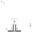
- FIG. 3 shows diagram of a wirelessly enabled functional block 300, according to an embodiment of the present invention.
- Wirelessly enabled functional block 300 includes an antenna 302.
- Wirelessly enabled functional blocks 210 and/or 212 can be implemented in a manner substantially similar to wirelessly enabled functional block 300.
- antenna 302 is a dipole antenna.
- antenna 302 can be formed out of metal traces or planes.
- dipole antenna 302 can be formed using traces on the bottom surface of IC die 204 or on the top surface of substrate 202.
- Antenna 302 can be configured to operate in a certain frequency range (e.g., by adjusting the dimensions of antenna 302).
- antenna 302 can be another type of antenna.
- antenna 302 can be a patch antenna having a square or rectangular shape.
- via 304a can be coupled to a signal plane.
- via 304a can be coupled to a signal plane of an IC die, e.g., signal plane 206.
- wirelessly enabled functional block 300 is formed on a substrate
- via 304a can be coupled to a signal plane of the substrate, e.g., a ground plane of the substrate.
- Via 304b can be coupled to circuit block of an IC die or a portion of substrate 202 from which a signal from a PCB is received.
- wirelessly enabled functional block optionally includes a transceiver 306.
- antenna 302 is fed by transceiver 306.
- Transceiver 306 can be coupled to a signal plane using vias of a die or substrate.
- tranceiver 306 is also coupled to a circuit block or a portion of a PCB (e.g., through a substrate).
- Tranceiver 306 can be configured to transmit signals received from the circuit block or the PCB and/or convey received signals to the circuit block or the PCB.
- transceiver 306 can have additional functionality.
- transceiver 306 may be capable of performing signal processing tasks such as modulation.
- FIG. 4 shows a cross-sectional view of a die down IC device 400, according to an embodiment of the present invention.
- IC device 400 is substantially similar to IC device 200 shown in FIG. 2 except that IC device 400 additionally includes a heat spreader 402.
- Heat spreader 402 is coupled to IC die 204 through an adhesive 404. Additionally, it can also be coupled to substrate 202 through an adhesive 406.
- Adhesives 404 and 406 can be thermally conductive so that heat can be spread from IC die 204 to substrate 202.
- adhesives 404 and 406 can be electrically conductive.
- signal plane 206 may be made up of single portion that is grounded.
- FIG. 5 shows a cross-sectional view of a die up IC device 500, according to an embodiment of the present invention.
- IC device 500 includes a substrate 502, an IC die 504, wirelessly enabled functional blocks 506a, 506b, and 506c (collectively “506"), wirelessly enabled functional blocks 508a, 508b, and 508c (collectively "508"), wirebonds 510a and 510a (collectively "510"), bond pads 512a and 512b (collectively "512”), and an adhesive 514.
- IC die 504 is coupled to substrate 502 through adhesive 514.
- substrate 502 is similar to substrate 120.
- IC die 504 can be similar to IC die 110 except that IC die 504 is implemented in a die up configuration, where the top surface of IC die 504 is the active surface.
- the active surface of IC die 504 can be the surface that contains containing layers that include integrated circuits.
- Wirelessly enabled functional blocks 506 and 508 enable IC die 504 to wirelessly communicate with substrate 502.
- wirelessly enabled functional blocks 506 and 508 are implemented similar to wirelessly enabled functional block 300, described with reference to FIG. 3 .
- Any of wirelessly enabled functional blocks 506 can be configured to communicate with any of wirelessly enabled functional blocks 508.
- frequency, time, and code division schemes can be used to prevent communications between one pair of wirelessly enabled functional blocks from interfering with communications between another pair of wirelessly enabled functional blocks.
- wirelessly enabled functional block 506c is larger than wirelessly enabled functional blocks 506a and 506b.
- wirelessly enabled functional block 506c has additional functionality compared to wirelessly enabled functional blocks 506a and 506b.
- wirelessly enabled functional block 506c may have additional signal processing functionality.
- IC device 500 also includes wire bonds 510 and bond pads 512.
- IC die 504 can communicate with substrate 502 through wirelessly enabled functional blocks 506 and 508 and -through bond pads 512 and wirebonds 510.
- Wire bonds 510 are coupled to bond fingers formed on substrate 502 (not shown).
- IC device 500 does not include wire bonds 510 and bond pads 512. In such an embodiment, all communications between substrate 502 and IC die 504 occur using wirelessly enabled functional blocks 506 and 508.
- FIG. 6 shows a cross-sectional view of a die up IC device 600, according to an embodiment of the present invention.
- IC device 600 is substantially similar to IC device 500 shown in FIG. 5 , except that IC device 600 additionally includes signal plane 602. Similar to signal plane 206, shown in FIG. 2 , signal plane 602 can include a single portion (e.g., a grounded portion) or multiple isolated signal portions having distinct voltages.
- signal plane 602 includes openings 604.
- openings 604 facilitate communications between wirelessly enabled functional blocks 506 and 508.
- signal plane 602 is formed out of an electrically conductive material. Thus, without openings 604, signal plane may interfere with communications between wirelessly enabled functional blocks 506 and 508.
- FIG. 7 shows a cross-sectional view of a die up IC device 700, according to an embodiment of the present invention.
- IC device 700 is substantially similar to IC device 600, shown in FIG. 6 except that IC device 700 additionally includes vias 702a and 702b (collectively "702").
- vias 702 couple respective blocks of wirelessly enabled functional blocks 506 to signal plane 602.
- vias 702 can couple respective wirelessly enabled functional blocks 506 to a ground portion of signal plane 602.
- FIG. 8 shows a signal plane 800, according to an embodiment of the present invention.
- signal plane 800 can be used for signal plane 602 shown in FIGS. 6 and 7 .
- Signal plane 800 includes portions 802 and 804. As shown in FIG. 8 , portions 802 and 804 are isolated (e.g., separated) so that they can have different potentials. For example, portion 802 can have a ground potential and portion 804 can have a power potential.
- FIG. 8 shows signal plane 800 as including two portions 802 and 804.
- signal plane 800 can include more than two portions.
- signal plane 800 can include multiple different portions held at different power potentials and a portion that is grounded.
- signal plane 800 can include a single portion, e.g., a single portion that is coupled to ground.
- signal plane 800 includes openings 806. Openings 806 can be used to facilitate communications between wirelessly enabled functional blocks. For example, when signal plane 800 is used in IC device 600, openings 806 can be used to facilitate communications between wirelessly enabled functional blocks 506 and 508. Openings 806 can be in any shape that facilitates the communications between wirelessly enabled functional blocks.
- FIG. 8 shows signal plane 800 as including four openings. However, as would be appreciated by those skilled in the relevant art based on the description herein, signal plane 800 can include any number of openings 806. In an alternate embodiment, signal plane 800 does not include any openings 806.
- FIG. 9 shows a signal plane 900, according to an embodiment of the present invention.
- Signal plane 900 is substantially similar to signal plane 800, shown in FIG. 8 , except that signal plane 900 additionally includes solder pads 902.
- solder pads 902 can be used to receive vias from an IC die, e.g., vias 702 in IC package 700 shown in FIG. 7 .
- the structure of signal plane 900 can be especially useful when signal plane 900 is implemented as a metallic tape. Such a metallic tape, would be coupled to a surface of an IC die.
- the metallic tape could be coupled to the bottom surface of IC die 504 in package 700 shown in FIG. 7 .
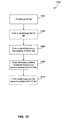
- FIG. 10 shows a flowchart 1000 providing example steps for assembling an IC device, according to an embodiment of the present invention.
- Other structural and operational embodiments will be apparent to persons skilled in the relevant art(s) based on the following discussion.
- the steps shown in FIG. 10 do not necessarily have to occur in the order shown.
- the steps of FIG. 10 are described in detail below.
- step 1002 an IC die is provided.
- IC die 204 shown in FIG. 4 or IC die 504 shown in FIG. 7 can be provided.
- a via is formed through the IC die.
- vias 208 can be formed through IC die 204.
- vias 702 can be formed through IC die 504.
- a signal plane is formed on a first surface of the IC die.
- signal plane 206 is formed on top surface of IC die 204.
- signal plane 602 is formed on the bottom surface of IC die 504.
- forming a signal plane can include coupling a signal plane to the first surface of the IC die.
- the signal plane can be a metallic tape that is adhered to the first surface of the IC die.
- the signal plane can be one or more sheets of metal coupled to the first surface of the IC through an adhesive.
- wirelessly enabled functional blocks are formed on a second surface of the IC die.
- wirelessly enabled functional blocks 210 are formed on the bottom surface of IC die 204.
- wirelessly enabled functional blocks 506 are formed on the top surface of IC die 504.
- contact pads are formed on the second surface of the IC die.
- contact pads 216 are formed on the bottom surface of IC die 204.
- forming the wirelessly enabled functional blocks can include forming one or more traces on the second surface of the IC die.
- antenna 302 can be formed out of one or more traces or metal islands (e.g., a square or rectangular patch antenna).
- Forming the wirelessly enabled functional block can also include coupling a transceiver to the second surface of the IC die, e.g., transceiver 306 shown in FIG. 3 .
- FIG. 11 shows a flowchart 1100 providing example steps for assembling an IC device, according to an embodiment of the present invention.
- FIG. 11 shows a flowchart 1100 providing example steps for assembling an IC device, according to an embodiment of the present invention.
- Other structural and operational embodiments will be apparent to persons skilled in the relevant art(s) based on the following discussion.
- the steps shown in FIG. 11 do not necessarily have to occur in the order shown.
- the steps of FIG. 1100 are described in detail below.
- step 1102 an IC die having wirelessly enabled functional blocks provided.
- the IC die resulting from flowchart 1000 can be provided.
- the IC die is coupled to a substrate having wirelessly enabled functional blocks.
- IC die 204 is coupled to substrate 202 through an adhesive 218.
- solder bumps 214 and contact pads 216 serve to electrically couple IC die 204 to substrate 202.
- IC die 504 is coupled to substrate 502 through an adhesive 514. Bond pads 512 and wire bonds 510 serve to provide additional electrical coupling between IC die 504 and substrate 502.
- a heat spreader is coupled to the IC die.
- heat spreader 402 is coupled to IC die 204 through an adhesive 404.
- heat spreader 402 is coupled to substrate 202 through adhesive 406.
Landscapes
- Semiconductor Integrated Circuits (AREA)
- Transceivers (AREA)
Applications Claiming Priority (2)
| Application Number | Priority Date | Filing Date | Title |
|---|---|---|---|
| US35788010P | 2010-06-23 | 2010-06-23 | |
| US13/022,277 US20110316139A1 (en) | 2010-06-23 | 2011-02-07 | Package for a wireless enabled integrated circuit |
Publications (2)
| Publication Number | Publication Date |
|---|---|
| EP2400545A2 true EP2400545A2 (de) | 2011-12-28 |
| EP2400545A3 EP2400545A3 (de) | 2013-08-28 |
Family
ID=44580448
Family Applications (1)
| Application Number | Title | Priority Date | Filing Date |
|---|---|---|---|
| EP11005016.8A Withdrawn EP2400545A3 (de) | 2010-06-23 | 2011-06-20 | Baugruppe für eine integrierte Schaltung mit Drahtlosfunktion |
Country Status (4)
| Country | Link |
|---|---|
| US (1) | US20110316139A1 (de) |
| EP (1) | EP2400545A3 (de) |
| CN (1) | CN102299140A (de) |
| TW (1) | TWI465161B (de) |
Families Citing this family (5)
| Publication number | Priority date | Publication date | Assignee | Title |
|---|---|---|---|---|
| US8901945B2 (en) | 2011-02-23 | 2014-12-02 | Broadcom Corporation | Test board for use with devices having wirelessly enabled functional blocks and method of using same |
| US8928139B2 (en) | 2011-09-30 | 2015-01-06 | Broadcom Corporation | Device having wirelessly enabled functional blocks |
| CN105390434A (zh) * | 2014-09-05 | 2016-03-09 | 中芯国际集成电路制造(上海)有限公司 | 一种半导体器件及其制备方法、电子装置 |
| EP3389136B1 (de) * | 2015-12-10 | 2021-04-14 | Panasonic Intellectual Property Management Co., Ltd. | Drahtlosmodul und bildanzeigevorrichtung |
| US11005161B2 (en) * | 2017-10-20 | 2021-05-11 | Qualcomm Incorporated | Multilayer bowtie antenna structure |
Family Cites Families (38)
| Publication number | Priority date | Publication date | Assignee | Title |
|---|---|---|---|---|
| JP2840493B2 (ja) * | 1991-12-27 | 1998-12-24 | 株式会社日立製作所 | 一体型マイクロ波回路 |
| US6728113B1 (en) * | 1993-06-24 | 2004-04-27 | Polychip, Inc. | Method and apparatus for non-conductively interconnecting integrated circuits |
| FR2727227B1 (fr) * | 1994-11-17 | 1996-12-20 | Schlumberger Ind Sa | Dispositif de securite actif a memoire electronique |
| JP3378435B2 (ja) * | 1995-09-29 | 2003-02-17 | 株式会社東芝 | 超高周波帯無線通信装置 |
| FR2765399B1 (fr) * | 1997-06-27 | 2001-12-07 | Sgs Thomson Microelectronics | Dispositif semi-conducteur a moyen d'echanges a distance |
| EP0932200A3 (de) * | 1998-01-22 | 2000-08-23 | International Business Machines Corporation | Kühlkörper für Mikroprozessor |
| EP0978729A3 (de) * | 1998-08-07 | 2002-03-20 | Hitachi, Ltd. | Hochfrequenz-Sende-Empfangsvorrichtung für Fahrzeug-Radarsysteme |
| US6542720B1 (en) * | 1999-03-01 | 2003-04-01 | Micron Technology, Inc. | Microelectronic devices, methods of operating microelectronic devices, and methods of providing microelectronic devices |
| JP3675688B2 (ja) * | 2000-01-27 | 2005-07-27 | 寛治 大塚 | 配線基板及びその製造方法 |
| JP4848108B2 (ja) * | 2001-09-14 | 2011-12-28 | インターナショナル・ビジネス・マシーンズ・コーポレーション | データ処理システム |
| US6885090B2 (en) * | 2001-11-28 | 2005-04-26 | North Carolina State University | Inductively coupled electrical connectors |
| US6670692B1 (en) * | 2002-10-09 | 2003-12-30 | Silicon Integrated Systems Corp. | Semiconductor chip with partially embedded decoupling capacitors |
| US7095620B2 (en) * | 2002-11-27 | 2006-08-22 | International Business Machines Corp. | Optically connectable circuit board with optical component(s) mounted thereon |
| US6956285B2 (en) * | 2003-01-15 | 2005-10-18 | Sun Microsystems, Inc. | EMI grounding pins for CPU/ASIC chips |
| US20050075080A1 (en) * | 2003-10-03 | 2005-04-07 | Nanyang Technological University | Inter-chip and intra-chip wireless communications systems |
| US7525199B1 (en) * | 2004-05-21 | 2009-04-28 | Sun Microsystems, Inc | Packaging for proximity communication positioned integrated circuits |
| JP4752369B2 (ja) * | 2004-08-24 | 2011-08-17 | ソニー株式会社 | 半導体装置および基板 |
| DE102004059333A1 (de) * | 2004-12-09 | 2006-06-14 | Robert Bosch Gmbh | Antennenanordnung für einen Radar-Transceiver |
| DE102004063541A1 (de) * | 2004-12-30 | 2006-07-13 | Robert Bosch Gmbh | Antennenanordnung für einen Radar-Transceiver |
| US20060285480A1 (en) * | 2005-06-21 | 2006-12-21 | Janofsky Eric B | Wireless local area network communications module and integrated chip package |
| US8390307B2 (en) * | 2006-03-07 | 2013-03-05 | Steven Slupsky | Method and apparatus for interrogating an electronic component |
| KR100691632B1 (ko) * | 2006-05-16 | 2007-03-12 | 삼성전기주식회사 | 반도체칩, 반도체칩의 제조방법 및 반도체칩 패키지 |
| US8008799B2 (en) * | 2006-06-21 | 2011-08-30 | Broadcom Corporation | Integrated circuit with supply line intra-chip clock interface and methods for use therewith |
| US20080122726A1 (en) * | 2006-11-27 | 2008-05-29 | Gil Levi | Low cost chip package with integrated RFantenna |
| US8032089B2 (en) * | 2006-12-30 | 2011-10-04 | Broadcom Corporation | Integrated circuit/printed circuit board substrate structure and communications |
| US7974587B2 (en) * | 2006-12-30 | 2011-07-05 | Broadcom Corporation | Local wireless communications within a device |
| WO2008094128A1 (en) * | 2007-01-29 | 2008-08-07 | Agency For Science, Technology And Research | Antenna for underwater communications |
| US8116294B2 (en) * | 2007-01-31 | 2012-02-14 | Broadcom Corporation | RF bus controller |
| US7518226B2 (en) * | 2007-02-06 | 2009-04-14 | Stats Chippac Ltd. | Integrated circuit packaging system with interposer |
| US20080237843A1 (en) * | 2007-03-27 | 2008-10-02 | Ashish Gupta | Microelectronic package including thermally conductive sealant between heat spreader and substrate |
| US7899407B2 (en) * | 2007-05-01 | 2011-03-01 | Broadcom Corporation | High frequency signal combining |
| US20090006675A1 (en) * | 2007-06-28 | 2009-01-01 | Broadcom Corporation | Universal Serial Bus Dongle Device with Millimeter Wave Transceiver and System for use Therewith |
| US7911388B2 (en) * | 2007-12-12 | 2011-03-22 | Broadcom Corporation | Method and system for configurable antenna in an integrated circuit package |
| US20090227205A1 (en) * | 2008-03-04 | 2009-09-10 | Broadcom Corporation | Inductively coupled integrated circuit with multiple access protocol and methods for use therewith |
| TWI370530B (en) * | 2008-05-21 | 2012-08-11 | Advanced Semiconductor Eng | Semiconductor package having an antenna |
| US8384596B2 (en) * | 2008-06-19 | 2013-02-26 | Broadcom Corporation | Method and system for inter-chip communication via integrated circuit package antennas |
| US8274147B2 (en) * | 2008-06-19 | 2012-09-25 | Broadcom Corporation | Method and system for intra-printed circuit board communication via waveguides |
| US7943404B2 (en) * | 2008-08-07 | 2011-05-17 | International Business Machines Corporation | Integrated millimeter wave antenna and transceiver on a substrate |
-
2011
- 2011-02-07 US US13/022,277 patent/US20110316139A1/en not_active Abandoned
- 2011-06-20 EP EP11005016.8A patent/EP2400545A3/de not_active Withdrawn
- 2011-06-22 TW TW100121819A patent/TWI465161B/zh not_active IP Right Cessation
- 2011-06-23 CN CN201110171002A patent/CN102299140A/zh active Pending
Also Published As
| Publication number | Publication date |
|---|---|
| CN102299140A (zh) | 2011-12-28 |
| TWI465161B (zh) | 2014-12-11 |
| EP2400545A3 (de) | 2013-08-28 |
| TW201215258A (en) | 2012-04-01 |
| US20110316139A1 (en) | 2011-12-29 |
Similar Documents
| Publication | Publication Date | Title |
|---|---|---|
| US10347552B2 (en) | Semiconductor device | |
| US6008534A (en) | Integrated circuit package having signal traces interposed between power and ground conductors in order to form stripline transmission lines | |
| CN107180826B (zh) | 半导体封装组件 | |
| CN102446906B (zh) | 集成电路器件及其制造方法 | |
| US20140217582A1 (en) | Semiconductor device | |
| US7772696B2 (en) | IC package having IC-to-PCB interconnects on the top and bottom of the package substrate | |
| US9349697B2 (en) | Microbump and sacrificial pad pattern | |
| US9589908B1 (en) | Methods to improve BGA package isolation in radio frequency and millimeter wave products | |
| US20040061223A1 (en) | Integrated circuit die and/or package having a variable pitch contact array for maximization of number of signal lines per routing layer | |
| US20110316139A1 (en) | Package for a wireless enabled integrated circuit | |
| CN103035628B (zh) | 具有无线激活功能块的装置 | |
| US11923349B2 (en) | Semiconductor structures | |
| KR20090098316A (ko) | 플립 칩 패키지 | |
| EP3171403A2 (de) | Chipgehäuse auf waferebene mit umverteilungsschicht | |
| US20240014092A1 (en) | Semiconductor package | |
| HK1165610A (en) | An integrated circuit device and method for preparation of the integrated circuit device | |
| HK1165902A (en) | Integrated circuit device and method of manufacturing the integrated circuit device | |
| CN117222105A (zh) | 一种高可靠性flip-chip工艺基板 | |
| HK1167929A (en) | Integrated circuit device and method for manufacturing the same | |
| HK1173555B (en) | Integrated circuit device and method of manufacturing the integrated circuit device |
Legal Events
| Date | Code | Title | Description |
|---|---|---|---|
| AK | Designated contracting states |
Kind code of ref document: A2 Designated state(s): AL AT BE BG CH CY CZ DE DK EE ES FI FR GB GR HR HU IE IS IT LI LT LU LV MC MK MT NL NO PL PT RO RS SE SI SK SM TR |
|
| AX | Request for extension of the european patent |
Extension state: BA ME |
|
| PUAI | Public reference made under article 153(3) epc to a published international application that has entered the european phase |
Free format text: ORIGINAL CODE: 0009012 |
|
| PUAL | Search report despatched |
Free format text: ORIGINAL CODE: 0009013 |
|
| AK | Designated contracting states |
Kind code of ref document: A3 Designated state(s): AL AT BE BG CH CY CZ DE DK EE ES FI FR GB GR HR HU IE IS IT LI LT LU LV MC MK MT NL NO PL PT RO RS SE SI SK SM TR |
|
| AX | Request for extension of the european patent |
Extension state: BA ME |
|
| RIC1 | Information provided on ipc code assigned before grant |
Ipc: H01L 23/48 20060101AFI20130719BHEP Ipc: H01L 23/522 20060101ALI20130719BHEP |
|
| 17P | Request for examination filed |
Effective date: 20140228 |
|
| RBV | Designated contracting states (corrected) |
Designated state(s): AL AT BE BG CH CY CZ DE DK EE ES FI FR GB GR HR HU IE IS IT LI LT LU LV MC MK MT NL NO PL PT RO RS SE SI SK SM TR |
|
| 17Q | First examination report despatched |
Effective date: 20151119 |
|
| STAA | Information on the status of an ep patent application or granted ep patent |
Free format text: STATUS: EXAMINATION IS IN PROGRESS |
|
| STAA | Information on the status of an ep patent application or granted ep patent |
Free format text: STATUS: THE APPLICATION IS DEEMED TO BE WITHDRAWN |
|
| 18D | Application deemed to be withdrawn |
Effective date: 20170103 |