EP2392691A1 - Organoaminosilane precursors and methods for depositing films comprising the same - Google Patents
Organoaminosilane precursors and methods for depositing films comprising the same Download PDFInfo
- Publication number
- EP2392691A1 EP2392691A1 EP11168589A EP11168589A EP2392691A1 EP 2392691 A1 EP2392691 A1 EP 2392691A1 EP 11168589 A EP11168589 A EP 11168589A EP 11168589 A EP11168589 A EP 11168589A EP 2392691 A1 EP2392691 A1 EP 2392691A1
- Authority
- EP
- European Patent Office
- Prior art keywords
- group
- precursor
- organoaminosilane
- alkyl group
- silyl
- Prior art date
- Legal status (The legal status is an assumption and is not a legal conclusion. Google has not performed a legal analysis and makes no representation as to the accuracy of the status listed.)
- Granted
Links
- 0 **(c1ccccc1)I Chemical compound **(c1ccccc1)I 0.000 description 4
Images




Classifications
-
- C—CHEMISTRY; METALLURGY
- C07—ORGANIC CHEMISTRY
- C07F—ACYCLIC, CARBOCYCLIC OR HETEROCYCLIC COMPOUNDS CONTAINING ELEMENTS OTHER THAN CARBON, HYDROGEN, HALOGEN, OXYGEN, NITROGEN, SULFUR, SELENIUM OR TELLURIUM
- C07F7/00—Compounds containing elements of Groups 4 or 14 of the Periodic Table
- C07F7/02—Silicon compounds
- C07F7/025—Silicon compounds without C-silicon linkages
-
- C—CHEMISTRY; METALLURGY
- C07—ORGANIC CHEMISTRY
- C07F—ACYCLIC, CARBOCYCLIC OR HETEROCYCLIC COMPOUNDS CONTAINING ELEMENTS OTHER THAN CARBON, HYDROGEN, HALOGEN, OXYGEN, NITROGEN, SULFUR, SELENIUM OR TELLURIUM
- C07F7/00—Compounds containing elements of Groups 4 or 14 of the Periodic Table
- C07F7/02—Silicon compounds
- C07F7/08—Compounds having one or more C—Si linkages
- C07F7/10—Compounds having one or more C—Si linkages containing nitrogen having a Si-N linkage
-
- C—CHEMISTRY; METALLURGY
- C23—COATING METALLIC MATERIAL; COATING MATERIAL WITH METALLIC MATERIAL; CHEMICAL SURFACE TREATMENT; DIFFUSION TREATMENT OF METALLIC MATERIAL; COATING BY VACUUM EVAPORATION, BY SPUTTERING, BY ION IMPLANTATION OR BY CHEMICAL VAPOUR DEPOSITION, IN GENERAL; INHIBITING CORROSION OF METALLIC MATERIAL OR INCRUSTATION IN GENERAL
- C23C—COATING METALLIC MATERIAL; COATING MATERIAL WITH METALLIC MATERIAL; SURFACE TREATMENT OF METALLIC MATERIAL BY DIFFUSION INTO THE SURFACE, BY CHEMICAL CONVERSION OR SUBSTITUTION; COATING BY VACUUM EVAPORATION, BY SPUTTERING, BY ION IMPLANTATION OR BY CHEMICAL VAPOUR DEPOSITION, IN GENERAL
- C23C16/00—Chemical coating by decomposition of gaseous compounds, without leaving reaction products of surface material in the coating, i.e. chemical vapour deposition [CVD] processes
- C23C16/22—Chemical coating by decomposition of gaseous compounds, without leaving reaction products of surface material in the coating, i.e. chemical vapour deposition [CVD] processes characterised by the deposition of inorganic material, other than metallic material
- C23C16/30—Deposition of compounds, mixtures or solid solutions, e.g. borides, carbides, nitrides
- C23C16/34—Nitrides
-
- C—CHEMISTRY; METALLURGY
- C23—COATING METALLIC MATERIAL; COATING MATERIAL WITH METALLIC MATERIAL; CHEMICAL SURFACE TREATMENT; DIFFUSION TREATMENT OF METALLIC MATERIAL; COATING BY VACUUM EVAPORATION, BY SPUTTERING, BY ION IMPLANTATION OR BY CHEMICAL VAPOUR DEPOSITION, IN GENERAL; INHIBITING CORROSION OF METALLIC MATERIAL OR INCRUSTATION IN GENERAL
- C23C—COATING METALLIC MATERIAL; COATING MATERIAL WITH METALLIC MATERIAL; SURFACE TREATMENT OF METALLIC MATERIAL BY DIFFUSION INTO THE SURFACE, BY CHEMICAL CONVERSION OR SUBSTITUTION; COATING BY VACUUM EVAPORATION, BY SPUTTERING, BY ION IMPLANTATION OR BY CHEMICAL VAPOUR DEPOSITION, IN GENERAL
- C23C16/00—Chemical coating by decomposition of gaseous compounds, without leaving reaction products of surface material in the coating, i.e. chemical vapour deposition [CVD] processes
- C23C16/22—Chemical coating by decomposition of gaseous compounds, without leaving reaction products of surface material in the coating, i.e. chemical vapour deposition [CVD] processes characterised by the deposition of inorganic material, other than metallic material
- C23C16/30—Deposition of compounds, mixtures or solid solutions, e.g. borides, carbides, nitrides
- C23C16/34—Nitrides
- C23C16/345—Silicon nitride
-
- C—CHEMISTRY; METALLURGY
- C23—COATING METALLIC MATERIAL; COATING MATERIAL WITH METALLIC MATERIAL; CHEMICAL SURFACE TREATMENT; DIFFUSION TREATMENT OF METALLIC MATERIAL; COATING BY VACUUM EVAPORATION, BY SPUTTERING, BY ION IMPLANTATION OR BY CHEMICAL VAPOUR DEPOSITION, IN GENERAL; INHIBITING CORROSION OF METALLIC MATERIAL OR INCRUSTATION IN GENERAL
- C23C—COATING METALLIC MATERIAL; COATING MATERIAL WITH METALLIC MATERIAL; SURFACE TREATMENT OF METALLIC MATERIAL BY DIFFUSION INTO THE SURFACE, BY CHEMICAL CONVERSION OR SUBSTITUTION; COATING BY VACUUM EVAPORATION, BY SPUTTERING, BY ION IMPLANTATION OR BY CHEMICAL VAPOUR DEPOSITION, IN GENERAL
- C23C16/00—Chemical coating by decomposition of gaseous compounds, without leaving reaction products of surface material in the coating, i.e. chemical vapour deposition [CVD] processes
- C23C16/22—Chemical coating by decomposition of gaseous compounds, without leaving reaction products of surface material in the coating, i.e. chemical vapour deposition [CVD] processes characterised by the deposition of inorganic material, other than metallic material
- C23C16/30—Deposition of compounds, mixtures or solid solutions, e.g. borides, carbides, nitrides
- C23C16/40—Oxides
- C23C16/401—Oxides containing silicon
-
- C—CHEMISTRY; METALLURGY
- C23—COATING METALLIC MATERIAL; COATING MATERIAL WITH METALLIC MATERIAL; CHEMICAL SURFACE TREATMENT; DIFFUSION TREATMENT OF METALLIC MATERIAL; COATING BY VACUUM EVAPORATION, BY SPUTTERING, BY ION IMPLANTATION OR BY CHEMICAL VAPOUR DEPOSITION, IN GENERAL; INHIBITING CORROSION OF METALLIC MATERIAL OR INCRUSTATION IN GENERAL
- C23C—COATING METALLIC MATERIAL; COATING MATERIAL WITH METALLIC MATERIAL; SURFACE TREATMENT OF METALLIC MATERIAL BY DIFFUSION INTO THE SURFACE, BY CHEMICAL CONVERSION OR SUBSTITUTION; COATING BY VACUUM EVAPORATION, BY SPUTTERING, BY ION IMPLANTATION OR BY CHEMICAL VAPOUR DEPOSITION, IN GENERAL
- C23C16/00—Chemical coating by decomposition of gaseous compounds, without leaving reaction products of surface material in the coating, i.e. chemical vapour deposition [CVD] processes
- C23C16/44—Chemical coating by decomposition of gaseous compounds, without leaving reaction products of surface material in the coating, i.e. chemical vapour deposition [CVD] processes characterised by the method of coating
- C23C16/50—Chemical coating by decomposition of gaseous compounds, without leaving reaction products of surface material in the coating, i.e. chemical vapour deposition [CVD] processes characterised by the method of coating using electric discharges
-
- H—ELECTRICITY
- H01—ELECTRIC ELEMENTS
- H01B—CABLES; CONDUCTORS; INSULATORS; SELECTION OF MATERIALS FOR THEIR CONDUCTIVE, INSULATING OR DIELECTRIC PROPERTIES
- H01B3/00—Insulators or insulating bodies characterised by the insulating materials; Selection of materials for their insulating or dielectric properties
- H01B3/02—Insulators or insulating bodies characterised by the insulating materials; Selection of materials for their insulating or dielectric properties mainly consisting of inorganic substances
- H01B3/12—Insulators or insulating bodies characterised by the insulating materials; Selection of materials for their insulating or dielectric properties mainly consisting of inorganic substances ceramics
Definitions
- organoaminosilane precursors that can be used for the deposition of dielectric films, including but not limited to, silicon containing films such as silicon nitride, silicon oxide, silicon carbo-nitride, and silicon oxynitride films are described herein.
- silicon containing films such as silicon nitride, silicon oxide, silicon carbo-nitride, and silicon oxynitride films are described herein.
- organoaminosilane precursors for depositing silicon-containing dielectric films in the fabrication of integrated circuit devices.
- the organoaminosilane precursors may be used for a variety of deposition processes, including but not limited to, atomic layer deposition ("ALD”), chemical vapor deposition (“CVD”), plasma enhanced chemical vapor deposition (“PECVD”), low pressure chemical vapor deposition (“LPCVD”), and atmospheric pressure chemical vapor deposition.
- ALD atomic layer deposition
- CVD chemical vapor deposition
- PECVD plasma enhanced chemical vapor deposition
- LPCVD low pressure chemical vapor deposition
- atmospheric pressure chemical vapor deposition atmospheric pressure chemical vapor deposition
- silicon-containing films such as, but not limited to, silicon oxide or silicon nitride films.
- these compounds suitable for use as precursors include silanes, chlorosilanes, polysilazanes, aminosilanes, and azidosilanes.
- Inert carrier gas or diluents such as, but not limited, helium, hydrogen, nitrogen, etc., are also used to deliver the precursors to the reaction chamber.
- Low pressure chemical vapor deposition (LPCVD) processes are one of the more widely accepted methods used by semiconductor industry for the deposition of silicon-containing films.
- Low pressure chemical vapor deposition (LPCVD) using ammonia may require deposition temperatures of greater than 750°C to obtain reasonable growth rates and uniformities. Higher deposition temperatures are typically employed to provide improved film properties.
- One of the more common industry methods to grow silicon nitride or other silicon-containing films is through low pressure chemical vapor deposition in a hot wall reactor at temperatures >750°C using the precursors silane, dichlorosilane, and/or ammonia.
- certain precursors, such as silane and dichlorosilane are pyrophoric.
- films deposited from silane and dichlorosilane may contain certain impurities.
- films deposited using dichlorosilane may contain certain impurities, such as chlorine and ammonium chloride, which are formed as byproducts during the deposition process.
- films deposited using silane may contain hydrogen.
- Precursors that are used in depositing silicon nitride films such as bis-tert-butylaminosilane ("BTBAS") and chlorosilanes generally deposit the films at temperatures greater than 550°C.
- BBAS bis-tert-butylaminosilane
- the trend of miniaturization of semiconductor devices and low thermal budget requires lower process temperature and higher deposition rate.
- the temperature, at which the silicon films are deposited, should decrease in order to prevent ion diffusion in the lattice, particularly for those substrates comprising metallization layers and on many Group III-V and II-VI devices.
- silicon-containing films such as silicon oxide or silicon nitride films that are sufficiently chemically reactive to allow deposition via CVD, ALD or other processes at temperatures of 550°C or below or even at room temperature.
- organoaminosilane precursors and methods using same for forming dielectric films comprising silicon such as, but not limited to, silicon oxide, silicon nitride, silicon oxynitride, silicon carbide, silicon carbonitride, and combinations thereof onto at least a portion of a substrate.
- methods to form dielectric films or coatings on an object to be processed such as, for example, a semiconductor wafer.
- a layer comprising silicon and oxygen is deposited onto a substrate using an organoaminosilane precursor and an oxidizing agent in a deposition chamber under conditions for generating a silicon oxide layer on the substrate.
- a layer comprising silicon and nitrogen is deposited onto a substrate using an organoaminosilane precursor and a nitrogen containing precursor in a deposition chamber under conditions for generating a silicon nitride layer on the substrate.
- the organoaminosilane precursors described herein can also be used a dopant for metal containing films, such as but not limited to, metal oxide films or metal nitride films.
- an organoaminosilane having Formula I is employed as at least one of the silicon containing precursors.
- an organoaminosilane precursor according to formula I wherein R 1 in formula I is independently selected from a hydrogen atom, a C 1 to C 20 (e.g. C 1 to C 6 ) alkyl group, a C 2 to C 20 (e.g. C 2 to C 6 ) alkenyl group, a C 2 to C 20 (e.g. C 2 to C 6 ) alkynyl group, a C 1 to C 20 (e.g. C 1 to C 6 ) alkoxy group, a C 2 to C 20 (e.g.
- n is a number selected from 0, 1, 2, 3, 4, and 5; and R 2 is independently selected from a hydrogen atom, a C 1 to C 20 (e.g. C 1 to C 6 ) alkyl group, a C 2 to C 20 (e.g. C 2 to C 6 ) alkenyl group, a C 2 to C 20 (e.g. C 2 to C 6 ) alkynyl group, a C 1 to C 20 (e.g. C 1 to C 6 ) alkoxy group, a C 1 to C 20 (e.g. C 1 to C 6 ) alkyl group with a C 1 to C 20 (e.g.
- C 1 to C 6 alkoxy group attached thereto, a C 1 to C 20 (e.g. C 1 to C 6 ) alkyl group with a C 2 to C 20 (e.g. C 2 to C 6 ) dialkylamino group attached thereto, a C 2 to C 20 (e.g. C 2 to C 6 ) dialkylamino group, a C 5 to C 12 (e.g. C 6 to C 10 ) aryl group, a C 1 to C 20 (e.g. C 1 to C 6 ) fluorinated alkyl group, and a C 3 to C 12 (e.g.
- R 1 and R 2 can be linked together to form a ring. In the yet further embodiments, R 1 and R 2 are not linked together to form a ring.
- a method for forming a silicon-containing film on at least one surface of a substrate by a deposition process selected from a chemical vapor deposition process and an atomic layer deposition process comprising reacting at least one organoaminosilane precursor according to the first aspect with either a nitrogen-containing source, or an oxidizing agent, to form said film on said surface.
- a silicon oxide film via an atomic layer deposition process comprising the steps of:
- a method of forming a silicon oxide film onto at least a surface of a substrate using a CVD process comprising:
- a silicon nitride film via an atomic layer deposition process comprising the steps of:
- a method of forming a silicon nitride film onto at least a surface of a substrate using a CVD process comprising:
- a vessel for depositing a dielectric film comprising one or more organoaminosilane precursor having Formula I comprises at least one pressurizable vessel (preferably of stainless steel) fitted with the proper valves and fittings to allow the delivery of one or more precursors to the reactor for a CVD or an ALD process.
- Organoaminosilanes, silane, or silicon-containing precursors are used as precursors to form stoichiometric and non-stoichiometric silicon containing films such as, but not limited to, silicon oxide, silicon oxycarbide, silicon nitride, silicon oxynitride and silicon oxycarbonitride. These precursors can also be used, for example, as dopants for metal containing films.
- the organoaminosilane precursors are typically high purity volatile liquid precursor chemical that are vaporized and delivered to a deposition chamber or reactor as a gas to deposit a silicon containing film via CVD or ALD processes for semiconductor devices. The selection of precursor materials for deposition depends upon the desired resultant dielectric material or film.
- a precursor material may be chosen for its content of chemical elements, its stoichiometric ratios of the chemical elements, and/or the resultant dielectric film or coating that are formed under CVD.
- the precursor material may also be chosen for various other characteristics such as cost, non-toxicity, handling characteristics, ability to maintain liquid phase at room temperature, volatility, molecular weight, and/or other considerations.
- the precursors described herein can be delivered to the reactor system by any number of means, preferably using a pressurizable stainless steel vessel fitted with the proper valves and fittings, to allow the delivery of liquid phase precursor to the deposition chamber or reactor.
- the organoaminosilanes precursors described herein exhibit a balance of reactivity and stability that makes them ideally suitable as CVD or ALD precursors.
- reactivity certain precursors may have boiling points that are too high to be vaporized and delivered to the reactor to be deposited as a film on a substrate.
- Precursors having higher relative boiling points require that the delivery container and lines need to be heated at or above the boiling point of the precursor to prevent condensation or particles from forming in the container, lines, or both.
- other precursors may form silane (SiH 4 ) as they degrade.
- Silane is pyrophoric at room temperature or it can spontaneously combust which presents safety and handling issues.
- the formation of silane and other by-products decreases the purity level of the precursor and changes as small as 1-2% in chemical purity may be considered unacceptable for reliable semiconductor manufacture.
- the organoaminosilane precursors having formula I comprise less than 2% by weight, or less than 1% by weight, or less than 0.5% by weight of by-product (such as the corresponding bis-silane byproduct) after being stored for a period of time of 6 months or more, or one year or more.
- the organoaminosilane precursor described herein may be able to deposit high density materials at relatively low deposition temperatures, e.g., at 500°C or less, at 400°C or less, or at 300°C or less.
- the organoaminosilane precursor such as phenylmethylaminosilane, can be used to deposit a dielectric film via ALD or PEALD at a temperature as low as 50°C or less, or at room temperature (e.g., 25°C).
- R 1 in formula I is independently selected from a hydrogen atom, a C 1 to C 20 alkyl group, a C 2 to C 20 alkenyl group, a C 2 to C 20 alkynyl group, a C 1 to C 20 alkoxy group, a C 2 to C 20 dialkylamino group and an electron withdrawing group; n is a number selected from 0, 1, 2, 3, 4, and 5; and R 2 is independently selected from a hydrogen atom, a C 1 to C 20 alkyl group, a C 2 to C 20 alkenyl group, a C 2 to C 20 alkynyl group, a C 1 to C 20 alkoxy group, a C 1 to C 20 alkyl group with a C 1 to C 20 alkoxy group attached thereto, a C 1 to C 20 alkyl group with a C 2 to C 20 dialkylamino group attached thereto, a C 2
- R 1 and R 2 can be linked together to form a ring. In alternative embodiments of the organoaminosilane of formula I, R 1 and R 2 are not linked together to form a ring.
- alkyl denotes a linear, or branched functional group having from 1 to 20, e.g. 1 to 12 or 1 to 6, carbon atoms.
- alkyl groups include, but are not limited to, methyl, ethyl, propyl, isopropyl, butyl, isobutyl, sec-butyl, tert-butyl, pentyl, iso-pentyl, tert-pentyl, hexyl, isohexyl, and neohexyl.
- the alkyl group may have one or more functional groups such as, but not limited to, an alkoxy group, a dialkylamino group or combinations thereof, or an electron withdrawing group, e.g. a nitrile group attached thereto. In other embodiments, the alkyl group does not have one or more functional groups attached thereto.
- cyclic alkyl denotes a cyclic functional group having from 3 to 12, e.g. from 4 to 10, carbon atoms.
- exemplary cyclic alkyl groups include, but are not limited to, cyclobutyl, cyclopentyl, cyclohexyl, and cyclooctyl groups.
- aryl denotes an aromatic cyclic functional group having from 5 to 12 carbon atoms, or from 6 to 10 carbon atoms.
- exemplary aryl groups include, but are not limited to, phenyl, benzyl, chlorobenzyl, tolyl, and o-xylyl.
- alkenyl group denotes a group which has one or more carbon-carbon double bonds and has from 2 to 20, e.g. from 2 to 12 or from 2 to 6, carbon atoms.
- alkynyl group denotes a group which has one or more carbon-carbon triple bonds and has from 2 to 20, e.g. from 2 to 12 or from 2 to 6, carbon atoms.
- alkoxy denotes an alkyl group which is linked to an oxygen atom (e.g., R-O) and may have from 1 to 20, e.g. from 1 to 12 or from 1 to 6, carbon atoms.
- exemplary alkoxy groups include, but are not limited to, methoxy (-OCH 3 ), ethoxy (-OCH 2 CH 3 ), n-propoxy (-OCH 2 CH 2 CH 3 ), and iso-propoxy (-OCHMe 2 ).
- dialkylamine group denotes a group which has two alkyl groups attached to a nitrogen atom and has from 2 to 20, e.g. from 2 to 12 or from 2 to 6, carbon atoms.
- electron withdrawing substituent describes an atom or group thereof that acts to draw electrons away from the Si-N bond.
- suitable electron withdrawing substituents include, but are not limited to, halogens (F, Cl, Br, I) and nitriles (CN).
- electron withdrawing substituent can be adjacent to or proximal to N in formula I.
- Further non-limiting examples of an electron withdrawing group includes F, Cl, Br, I, CN, NO 2 , RSO, and/or RSO 2 wherein R can be a C 1 to C 10 alkyl group such as, but not limited to, a methyl group or another group.
- one or more of the alkyl group, alkenyl group, alkynyl group, alkoxy group, dialkylamino group, aryl group, and/or electron withdrawing group in formula I (and II - see below) may be substituted or have one or more atoms or group of atoms substituted in place of, for example, a hydrogen atom.
- substituents include, but are not limited to, oxygen, sulfur, halogen atoms (e.g., F, Cl, I, or Br), nitrile, nitrogen, and phosphorous.
- one or more of the alkyl group, alkenyl group, alkynyl group, alkoxy group, dialkylamino aryl group, and/or electron withdrawing group in Formula I and II may be unsubstituted.
- substituents R 1 and R 2 are linked in formula I to form a ring structure. In other embodiments, substituent R 1 and R 2 are not linked in formula I.
- R 1 is the same. An example of this can be an embodiment wherein n is 2 and the two R 1 substituents are both methyl groups. In other embodiments wherein n in formula I is a number greater than 1, R 1 is different. An example of this can be an embodiment wherein n is 2 and the two R 1 substituents are a methyl group and a Cl atom. In these or other embodiments, R 1 and R 2 are independent of each other. In alternative embodiments wherein n in formula I is a number greater than 1, one of substituents R 1 and R 2 are linked in formula I to form a ring structure.
- the at least one organoaminosilane precursor having formula I has one or more substituents comprising oxygen atoms. In these embodiments, the need for an oxygen source during the deposition process may be avoided. In other embodiments, the at least one organoaminosilane precursor having formula I has one or more substituents comprising oxygen atoms also uses an oxygen source. In this or other embodiments, substituents R 1 and R 2 are linked via an oxygen atom in formula I to form a ring structure.
- Table 1 provides some non-limiting examples of certain embodiments of the organoaminosilanes having formula I.
- organoaminosilane precursors such as those organoaminosilanes having formula I described herein and having a -SiH 3 group are advantageous over other organoaminosilane precursors containing SiH 2 or -SiH groups because of its lower activation barrier to react on a hydroxylated semi-conductor surface (thus lower deposition temperature), lower impurity and higher film density after deposition.
- organoaminosilane precursors having a -SiH 3 group such as dimethylaminosilane (DMAS) or diethylaminosilane (DEAS) may not be thermally stable because it undergoes a disproportionational reaction to form pyrophoric silane and bis(dimethylamino)silane or bis(diethylamino)silane, respectively. It has been found that the activation barrier for PMAS was relatively low compared with DMAS. Further, it is thought that films deposited using these particular organoaminosilane precursors may contain appropriate levels and types of carbon in silicon nitride or silicon carbonitride networks that may enable a significant reduction in wet etch rate yet maintaining a certain dielectric constant value.
- DMAS dimethylaminosilane
- DEAS diethylaminosilane
- organoaminosilane precursors having Formula I described herein may allow for lower temperature depositions, such as, for example, room temperature depositions, than other organoaminosilanes known in the art such as diispropylaminosilane.
- the organoaminosilanes having formula I can be prepared by reacting a monochlorosilane (MCS) or lower molecular dialkylaminosilane such as di-iso-propylaminosilane with an amine having the following Formula II in an organic solvent or solvent mixture.
- MCS monochlorosilane
- amine having the following Formula II in an organic solvent or solvent mixture.
- R 1 , R 2 and n are as defined above.
- Exemplary amines having formula II wherein R 1 is hydrogen, a linear or branched C 1 to C 6 alkyl group, halide and R 2 is a linear or branched C 1 to C 6 alkyl group or a C 4 to C 10 cyclic alkyl include, but are not limited to, N-methylaniline, N-ethylaniline, N-iso-propylaniline, n-Butylaniline , N-allylaniline, N-Ethyl-m-toluidine, N-Methyl-o-toluidine, N-Methyl-p-toluidine, 4-fluoro-N-methylaniline, 4-Chloro-N-methylaniline, N-cyclohexylaniline, 3-anilinopropionitrile, or N-phenylglycinonitrile.
- Exemplary amines having formula II wherein R 1 and R 2 are linked to form a ring include, but are not limited to, 3-methylindole, 2-methylindole, indole, tetrahydroquinoline, 8-methyl-1,2,3,4-tetrahydroquinoline, 3-indoleacetonitrile, 2-methylindoline, 2,3-dihydroindole, 5-methylindoline, 1,2,3,4-tetrahydroquinoline, 1,2,3,4-tetrahydro-2-methylquinoline, 1,2,3,4-tetrahydro-6-methylquinoline, 3,4-dihydro-2H-1,4-benzoxazine, carbazole, and 3,6-dibromocarbazole.
- Equations 1 through 3 provide examples of reaction schemes or synthesis routes which may be used to make the organoaminosilanes having formula I as described herein.
- Reaction schemes 1 through 3 can be conducted with (e.g., in the presence of) or without (e.g., in the absence of) organic solvents.
- suitable organic solvents include, but are not limited to, hydrocarbon such as hexanes, octane, toluene, and ethers such as diethylether, and tetrahydrofuran (THF).
- the reaction temperature is in the range of from about -70°C to the boiling point of the solvent employed if a solvent is involved.
- Equation 1 is an embodiment involving a silyl exchange reaction. An example of this synthetic route is provided herein as Example 1.
- Equation 2 is an embodiment wherein a chlorinated silane is used as a reagent. An example of this synthetic route is provided herein as Example 2.
- Equation 3 is an embodiment wherein a metal amide such as a lithium or potassium amide and a chlorinated silane are used as reagents and results in the desired end product and a metal halide by-product.
- the method used to form the silicon-containing dielectric films or coatings are deposition processes.
- suitable deposition processes for the method disclosed herein include, but are not limited to, cyclic CVD (CCVD), MOCVD (Metal Organic CVD), thermal chemical vapor deposition, plasma enhanced chemical vapor deposition ("PECVD”), high density PECVD, photon assisted CVD, plasma-photon assisted (“PPECVD”), cryogenic chemical vapor deposition, chemical assisted vapor deposition, hot-filament chemical vapor deposition, CVD of a liquid polymer precursor, deposition from supercritical fluids, and low energy CVD (LECVD).
- the metal containing films are deposited via atomic layer deposition (ALD), plasma enhanced ALD (PEALD) or plasma enhanced cyclic CVD (PECCVD) process.
- ALD atomic layer deposition
- PEALD plasma enhanced ALD
- PECCVD plasma enhanced cyclic CVD
- chemical vapor deposition processes refers to any process wherein a substrate is exposed to one or more volatile precursors, which react and/or decompose on the substrate surface to produce the desired deposition.
- atomic layer deposition process refers to a self-limiting (e.g., the amount of film material deposited in each reaction cycle is constant), sequential surface chemistry that deposits films of materials onto substrates of varying compositions.
- the precursors, reagents and sources used herein may be sometimes described as "gaseous", it is understood that the precursors can be either liquid or solid which are transported with or without an inert gas into the reactor via direct vaporization, bubbling or sublimation.
- the vaporized precursors can pass through a plasma generator.
- the dielectric film is deposited using an ALD process.
- the dielectric film is deposited using a CCVD process.
- the dielectric film is deposited using a thermal CVD process.
- reactor as used herein, includes without limitation, reaction chamber or deposition chamber.
- the method disclosed herein avoids pre-reaction of the precursors by using ALD or CCVD methods that separate the precursors prior to and/or during the introduction to the reactor.
- deposition techniques such as ALD or CCVD processes are used to deposit the dielectric film.
- the film is deposited via an ALD process by exposing the substrate surface alternatively to the one or more the silicon-containing precursor, oxygen source, nitrogen-containing source, or other precursor or reagent. Film growth proceeds by self-limiting control of surface reaction, the pulse length of each precursor or reagent, and the deposition temperature. However, once the surface of the substrate is saturated, the film growth ceases.
- the method described herein further comprises one or more additional silicon-containing precursors other than the organoaminosilane precursor having the above formula I.
- additional silicon-containing precursors include, but are not limited to, organo-silicon compounds such as siloxanes (e.g., hexamethyl disiloxane (HMDSO) and dimethyl siloxane (DMSO)); organosilanes (e.g., methylsilane; dimethylsilane; vinyl trimethylsilane; trimethylsilane; tetramethylsilane; ethylsilane; disilylmethane; 2,4-disilapentane; 1,4-disilabutane; 2,5-disilahexane; 2,2-disilylpropane; 1,3,5-trisilacyclohexane, and fluorinated derivatives of these compounds; phenyl-containing organo-silicon compounds (e.g., dimethylphenylsi
- the one or more silicon-containing precursors may be introduced into the reactor at a predetermined molar volume, or from about 0.1 to about 1000 micromoles.
- the silicon-containing and/or organoaminosilane precursor may be introduced into the reactor for a predetermined time period. In certain embodiments, the time period ranges from about 0.001 to about 500 seconds.
- the dielectric films deposited using the methods described herein are formed in the presence of oxygen using an oxygen source, reagent or precursor comprising oxygen.
- An oxygen source may be introduced into the reactor in the form of at least one oxygen source and/or may be present incidentally in the other precursors used in the deposition process.
- Suitable oxygen source gases may include, for example, water (H 2 O) (e.g., deionized water, purified water, and/or distilled water), oxygen (O 2 ), oxygen plasma, ozone (O 3 ), NO, NO 2 , carbon monoxide (CO), carbon dioxide (CO 2 ) and combinations thereof.
- the oxygen source comprises an oxygen source gas that is introduced into the reactor at a flow rate ranging from about 1 to about 2000 square cubic centimeters (sccm) or from about 1 to about 1000 sccm.
- the oxygen source can be introduced for a time that ranges from about 0.1 to about 100 seconds.
- the oxygen source comprises water having a temperature of 10°C or greater.
- the precursor pulse can have a pulse duration that is greater than 0.01 seconds, and the oxygen source can have a pulse duration that is less than 0.01 seconds, while the water pulse duration can have a pulse duration that is less than 0.01 seconds.
- the purge duration between the pulses that can be as low as 0 seconds or is continuously pulsed without a purge in-between.
- the oxygen source or reagent is provided in a molecular amount less than a 1:1 ratio to the silicon precursor, so that at least some carbon is retained in the as deposited dielectric film.
- the dielectric films comprise silicon and nitrogen.
- the dielectric films deposited using the methods described herein are formed in the presence of nitrogen-containing source.
- An nitrogen-containing source may be introduced into the reactor in the form of at least one nitrogen source and/or may be present incidentally in the other precursors used in the deposition process.
- Suitable nitrogen-containing source gases may include, for example, ammonia, hydrazine, monoalkylhydrazine, dialkylhydrazine, nitrogen, nitrogen/hydrogen, ammonia plasma, nitrogen plasma, nitrogen/hydrogen plasma, and mixture thereof.
- the nitrogen-containing source comprises an ammonia plasma or hydrogen/nitrogen plasma source gas that is introduced into the reactor at a flow rate ranging from about 1 to about 2000 square cubic centimeters (sccm) or from about 1 to about 1000 sccm.
- the nitrogen-containing source can be introduced for a time that ranges from about 0.1 to about 100 seconds.
- the precursor pulse can have a pulse duration that is greater than 0.01 seconds
- the nitrogen-containing source can have a pulse duration that is less than 0.01 seconds
- the water pulse duration can have a pulse duration that is less than 0.01 seconds.
- the purge duration between the pulses that can be as low as 0 seconds or is continuously pulsed without a purge in-between.
- the deposition methods disclosed herein may involve one or more purge gases.
- the purge gas which is used to purge away unconsumed reactants and/or reaction byproducts, is an inert gas that does not react with the precursors.
- Exemplary purge gases include, but are not limited to, argon (Ar), nitrogen (N 2 ), helium (He), neon (Ne), hydrogen (H 2 ), and mixtures thereof.
- a purge gas such as Ar is supplied into the reactor at a flow rate ranging from about 10 to about 2000 sccm for about 0.1 to 1000 seconds, thereby purging the unreacted material and any byproduct that may remain in the reactor.
- the respective step of supplying the precursors, oxygen source, the nitrogen-containing source, and/or other precursors, source gases, and/or reagents may be performed by changing the time for supplying them to change the stoichiometric composition of the resulting dielectric film.
- Energy is applied to the at least one of the precursor, nitrogen-containing source, reducing agent, other precursors or combination thereof to induce reaction and to form the dielectric film or coating on the substrate.
- energy can be provided by, but not limited to, thermal, plasma, pulsed plasma, helicon plasma, high density plasma, inductively coupled plasma, X-ray, e-beam, photon, remote plasma methods, and combinations thereof.
- a secondary RF frequency source can be used to modify the plasma characteristics at the substrate surface.
- the plasma-generated process may comprise a direct plasma-generated process in which plasma is directly generated in the reactor, or alternatively a remote plasma-generated process in which plasma is generated outside of the reactor and supplied into the reactor.
- the organoaminosilane precursors and/or other silicon-containing precursors may be delivered to the reaction chamber such as a CVD or ALD reactor in a variety of ways.
- a liquid delivery system may be utilized.
- a combined liquid delivery and flash vaporization process unit may be employed, such as, for example, the turbo vaporizer manufactured by MSP Corporation of Shoreview, MN, to enable low volatility materials to be volumetrically delivered, which leads to reproducible transport and deposition without thermal decomposition of the precursor.
- the precursors described herein may be delivered in neat liquid form, or alternatively, may be employed in solvent formulations or compositions comprising same.
- the precursor formulations may include solvent component(s) of suitable character as may be desirable and advantageous in a given end use application to form a film on a substrate.
- a vessel for depositing a dielectric film comprising one or more organoaminosilane precursor having formula I comprises at least one pressurizable vessel (preferably of stainless steel) fitted with the proper valves and fittings to allow the delivery of one or more precursors to the reactor for a CVD or an ALD process.
- the organoaminosilane precursor of Formula I is provided in a pressurizable vessel comprised of stainless steel and the purity of the precursor is 98% by weight or greater or 99.5% or greater which is suitable for the majority of semiconductor applications.
- such vessels can also have means for mixing the precursors with one or more additional precursor if desired.
- the contents of the vessel(s) can be premixed with an additional precursor.
- the organoaminosilane precursor and/or other precursor can be maintained in separate vessels or in a single vessel having separation means for maintaining the organoaminosilane precursor and other precursor separate during storage.
- a cyclic deposition process such as CCVD, ALD, or PEALD may be employed, wherein at least one silicon-containing precursor selected from an organoaminosilane precursor having Formula I and optionally a nitrogen-containing source such as, for example, ammonia, hydrazine, monoalkylhydrazine, dialkylhydrazine, nitrogen, nitrogen/hydrogen, ammonia plasma, nitrogen plasma, nitrogen/hydrogen plasma are employed.
- a nitrogen-containing source such as, for example, ammonia, hydrazine, monoalkylhydrazine, dialkylhydrazine, nitrogen, nitrogen/hydrogen, ammonia plasma, nitrogen plasma, nitrogen/hydrogen plasma are employed.
- the gas lines connecting from the precursor canisters to the reaction chamber are heated to one or more temperatures depending upon the process requirements and the container of the organoaminosilane precursor having Formula I is kept at one or more temperatures for bubbling.
- a solution comprising the at least one silicon-containing precursor having Formula I is injected into a vaporizer kept at one or more temperatures for direct liquid injection.
- a flow of argon and/or other gas may be employed as a carrier gas to help deliver the vapor of the at least one organoaminosilane precursor to the reaction chamber during the precursor pulsing.
- the reaction chamber process pressure is about 1 Torr ( ⁇ 133 Pa).
- the substrate such as a silicon oxide substrate is heated on a heater stage in a reaction chamber that is exposed to the silicon-containing precursor initially to allow the complex to chemically adsorb onto the surface of the substrate.
- a purge gas such as argon purges away unabsorbed excess complex from the process chamber.
- a nitrogen-containing source may be introduced into reaction chamber to react with the absorbed surface followed by another gas purge to remove reaction by-products from the chamber.
- the process cycle can be repeated to achieve the desired film thickness.
- the steps of the methods described herein may be performed in a variety of orders, may be performed sequentially or concurrently (e.g., during at least a portion of another step), and any combination thereof.
- the respective step of supplying the precursors and the nitrogen-containing source gases may be performed by varying the duration of the time for supplying them to change the stoichiometric composition of the resulting dielectric film.
- the films containing both silicon and nitrogen are formed using a ALD deposition method that comprises the steps of:
- the dielectric films is formed using a ALD deposition method that comprises the steps of:
- the above steps define one cycle for the method described herein; and the cycle can be repeated until the desired thickness of a dielectric film is obtained.
- the steps of the methods described herein may be performed in a variety of orders, may be performed sequentially or concurrently (e.g., during at least a portion of another step), and any combination thereof.
- the respective step of supplying the precursors and oxygen source may be performed by varying the duration of the time for supplying them to change the stoichiometric composition of the resulting dielectric film, although always using oxygen in less than a stoichiometric amount relative to the available silicon.
- the dielectric film is deposited using a thermal CVD process.
- the method comprises:
- the above steps define one cycle for the method described herein; and the cycle can be repeated until the desired thickness of a dielectric film is obtained.
- the steps of the methods described herein may be performed in a variety of orders, may be performed sequentially or concurrently (e.g., during at least a portion of another step), and any combination thereof.
- the respective step of supplying the precursors and oxygen source may be performed by varying the duration of the time for supplying them to change the stoichiometric composition of the resulting dielectric film, although always using oxygen in less than a stoichiometric amount relative to the available silicon.
- other precursors such as silicon-containing precursors, nitrogen-containing precursors, oxygen sources, reducing agents, and/or other reagents can be alternately introduced into the reactor chamber.
- the dielectric film is deposited using a thermal CVD process.
- the method comprises:
- the organoaminosilane precursors having Formula I described herein can also be used a dopant for metal containing films, such as but not limited to, metal oxide films or metal nitride films.
- the metal containing film is deposited using an ALD or CVD process such as those processes described herein using metal alkoxide, metal amide, or volatile organometallic precursors.
- suitable metal alkoxide precursors that may be used with the method disclosed herein include, but are not limited to, group 3 to 6 metal alkoxide, group 3 to 6 metal complexes having both alkoxy and alkyl substituted cyclopentadienyl ligands, group 3 to 6 metal complexes having both alkoxy and alkyl substituted pyrrolyl ligands, group 3 to 6 metal complexes having both alkoxy and diketonate ligands; group 3 to 6 metal complexes having both alkoxy and ketoester ligands;
- suitable metal amide precursors that may be used with the method disclosed herein include, but are not limited to, tetrakis(dimethylamino)zirconium (TDMAZ), tetrakis(diethylamino)zirconium (TDEAZ), tetrakis(ethylmethylamino)zirconium (TEMAZ), tetrakis(dimethylamino)
- organometallic precursors that may be used with the method disclosed herein include, but are not limited to, group 3 metal cyclopentadienyls or alkyl cyclopentadienyls.
- exemplary Group 3 to 6 metal herein include, but not limited to, Y, La, Ce, Pr, Nd, Sm, Eu, Gd, Tb, Dy, Er, Yb, Lu, Ti, Hf, Zr, V, Nb, Ta, Cr, Mo, and W.
- the resultant dielectric films or coatings can be exposed to a post-deposition treatment such as, but not limited to, a plasma treatment, chemical treatment, ultraviolet light exposure, electron beam exposure, and/or other treatments to affect one or more properties of the film.
- a post-deposition treatment such as, but not limited to, a plasma treatment, chemical treatment, ultraviolet light exposure, electron beam exposure, and/or other treatments to affect one or more properties of the film.
- the dielectric films described herein have a dielectric constant of 6 or less. In these or other embodiments, the films can a dielectric constant of about 5 or below, or about 4 or below, or about 3.5 or below. However, it is envisioned that films having other dielectric constants (e.g., higher or lower) can be formed depending upon the desired end-use of the film.
- the method described herein may be used to deposit a silicon-containing film on at least a portion of a substrate.
- suitable substrates include but are not limited to, silicon, SiO 2 , Si 3 N 4 , OSG, FSG, silicon carbide, hydrogenated silicon carbide, silicon nitride, hydrogenated silicon nitride, silicon carbonitride, hydrogenated silicon carbonitride, boronitride, antireflective coatings, photoresists, organic polymers, porous organic and inorganic materials, metals such as copper and aluminum, and diffusion barrier layers such as but not limited to TiN, Ti(C)N, TaN, Ta(C)N, Ta, W, or WN.
- the films are compatible with a variety of subsequent processing steps such as, for example, chemical mechanical planarization (CMP) and anisotropic etching processes.
- CMP chemical mechanical planarization
- the deposited films have applications, which include, but are not limited to, computer chips, optical devices, magnetic information storages, coatings on a supporting material or substrate, microelectromechanical systems (MEMS), nanoelectromechanical systems, thin film transistor (TFT), and liquid crystal displays (LCD).
- MEMS microelectromechanical systems
- TFT thin film transistor
- LCD liquid crystal displays
- the end-product was characterized by mass spectroscopy (MS) which is provided in Figure 1 and shows, among other things, peaks at 137, 122, 106, 91, and 77.
- MS mass spectroscopy
- the product phenylmethylaminosilane (51.3g, 75% yield) was obtained by vacuum distillation with boiling point of 60 C at 5 mm Hg (-0.7 kPa). The compound was characterized by mass spectroscopy and confirms that the product is phenylmethylaminosilane.
- a comparison of Examples 1 and 2 shows that the synthesis method of Example 1 provided a higher product yield and is more convenient in lab scale synthesis.
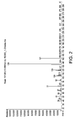
- the end-product was characterized by mass spectroscopy (MS) which is provided in Figure 2 and shows, among other things, peaks at 151, 150, 136, 120, 106, 93, and 77.
- MS mass spectroscopy
- the molecular weight of the phenylethylaminosilane was 151.28.
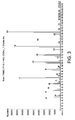
- the end-product was characterized by mass spectroscopy (MS) which is provided in Figure 3 and shows, among other things, peaks at 163, 162, 148, 136, 120, 107, 93, and 77.
- MS mass spectroscopy
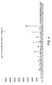
- the end-product was characterized by mass spectroscopy (MS) which is provided in Figure 4 and shows, among other things, peaks at 163, 162, 148, 132, 117, 105, 91, and 77.
- MS mass spectroscopy
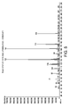
- the end-product was characterized by mass spectroscopy (MS) which is provided in Figure 5 and shows, among other things, peaks at 205, 178, 162, 132, 115, 93, and 77.
- MS mass spectroscopy
- the molecular weight of the phenylcyclohexylaminosilane was 205.37.
- a quantum mechanical method based on PM3 using SPARTAN06 simulation package was used to study the relative chemical stability of several precursors against ⁇ -H migration and disproportionation reaction.
- quantum mechanical density functional theory extensive calculations were conducted using computer modeling software to systematically evaluate the reaction energies of various SiN precursors. The calculations were done under the generalized gradient approximation (GGA) using the exchange-correlation functional proposed by Perdew-Wang (PW91) coupled with the double numerical atomic basis set augmented with polarization functions. All molecular structures were fully optimized to obtain the energetically most favorable geometries.
- the precursors used in the computer analysis are as follows: dimethylaminosilane (DMAS) and the precursor having Formula I described herein or phenylmethylaminosilane (PMAS).
- the reconstructed and fully hydroxylated SiO 2 (001) surface was modeled with a slab containing 6-layers alternated with two layers of O atoms and one layer of Si atoms, which is the preferred surface orientation for silica (see Figure 1 (A)).
- the top two layers of O atoms are all terminated by H atoms, representing the fully hydroxylated surface.
- the selected super cell contains 8 Si atoms, 20 O atoms and 8 H atoms, in addition to a precursor molecule. Prior to the precursor deposition, the surface was fully equilibrated.
- the optimized main structural parameters, shown in Table 2, are in good agreement with the experimental values and previous DFT calculations.
- a simulated atomic layer deposition process to develop a SiO 2 film using a Si precursor takes two successive steps.
- a silicon precursor is vaporized and then introduced onto a hydroxylated Si surface.
- reaction occurs on the surface with Si attacking the surface O on the hydroxyl group and the H of the hydroxyl group attacks the amino group of the precursor.
- the reaction leads to formation of a surface Si-O bond and liberation of an amine molecule into the gas-phase.
- an oxygen source such as O 3 or O 2 molecules are introduced to oxidize the Si-H bonds.
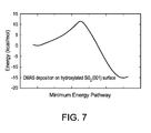
- the first principles DFT calculations were performed to investigate the minimum energy pathway of DMAS deposition on the fully hydroxylated SiO 2 (001) surface.
- the calculated energy profile is shown in Figure 7 .
- the simulation yields a thermochemical energy of-15.1 kcal/mol and activation barrier of 11.5 kcal/mol.
- the results suggest that DMAS is a reactive precursor and can be deposited on the surface with favorable thermodynamics and a low activation barrier.
- DMAS is not thermally stable and can readily undergo the following disproportionational reaction at ambient conditions: 2 (CH 3 ) 2 NSiH 3 ⁇ (CH 3 ) 2 NSiH 2 N(CH 3 ) 2 + SiH 4
- the calculated thermochemical energy and activation barrier for this reaction are -0.6 kcal/mol and 5.4 kcal/mol, respectively. While the reaction is essentially thermochemically neutral, the exceedingly low activation barrier promotes the disproportionational reaction at room temperature, indicating DMAS is not stable.
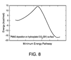
- the first principles DFT calculations were performed to investigate the minimum energy pathway of PMAS deposition on the fully hydroxylated SiO 2 (001) surface.
- the calculated energy profile is shown in Fig. 8 .
- the simulation yields a thermochemical energy of -16.9 kcal/mol and activation barrier of 14.1 kcal/mol.
- the results suggest that PMAS has an activation barrier only approximately 2.6 kcal/mol higher than that of DMAS. However, it is thermochemically much more exothermic.
- the results of the computer simulation indicate that PMAS can be deposited on the surface with favorable thermodynamics and a low activation barrier. Table 2.
- the selected bond parameters compared with reported values Bond parameters In this study Ref.
- Atomic layers depositions of silicon oxide films were conducted using the organoaminosilane precursor phenylmethylaminosilane (PMAS) to verify the results of the computer simulation in Example 7.
- the depositions were performed on a laboratory scale ALD processing tool starting at 150°C and temperatures were reduced until room temperature or the precursor failed to generate an oxide film.
- the process steps that were used to deposit the SiO 2 films are shown in Table 3.
- Depositions were performed using a baseline of 500 cycles with ozone as the oxygen source gas and the process parameters of the depositions are provided in Table 3.
- the resultant SiO 2 films were characterized for deposition rate, refractive index and % non-uniformity.
- the refractive index of the films was measured using a FilmTek 2000SE ellipsometer by fitting the reflection data from the film to a pre-set physical model (e.g., the Lorentz Oscillator model). For refractive index, a value of around 1.44 to 1.47 would reflect a typical CVD silicon oxide film. All of the precursors tested deposited films having a refractive index of ranging from about 1.4 to about 1.5.
- Atomic layers depositions of silicon oxide films were conducted using the organoaminosilane precursors phenylmethylaminosilane (PMAS), and diispropylaminosilane (DIPAS) using the ALD process described in Table 3.
- the depositions were performed on a laboratory scale ALD processing tool at the temperatures shown on the y axis of Figure 9 (e.g., 23°C or room temperature, 50°C, 75°C, and 100°C).
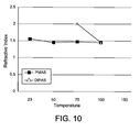
- the resultant silicon oxide films were characterized for deposition rate/cycle, and refractive index and the results are also provided in Figure 9 and 10 .
- the deposition rate per cycle is measured as Angstroms ( ⁇ )/cycle.
- the refractive index of the films was measured using a FilmTek 2000SE ellipsometer by fitting the reflection data from the film to a pre-set physical model (e.g., the Lorentz Oscillator model). As previously mentioned, for refractive index, a value of around 1.44 to 1.47 would reflect a typical CVD silicon oxide film.
- Figures 9 and 10 provide the relative deposition results and refractive indices for ALD deposited silicon oxide films using the two precursors.
- Figure 9 shows that for the same process conditions and ozone exposure time, PMAS appears to be in an ALD process window through 50°C.
- Figure 9 also shows that DIPAS did not deposit films below 100°C under the process conditions used in the example.
- Figure 10 indicates that both DIPAS and PMAS precursors yield silicon oxide films with good refractive indices for ALD oxide at around 100°C. However, for silicon oxide films deposited using DIPAS at 75°C, the refractive index for the film then increases, possibly due to impurities in the film (carbon containing ligands).
- the organoaminosilane precursor phenylmethylaminosilane was investigated for its effect as a silicon source on the deposition process to form silicon nitride films and the properties of the thin films deposited.
- the thin film deposition was performed using a LPCVD horizontal furnace or an ATV PEO 612 furnace.
- the working pressure for the deposition was ⁇ 1Torr ( ⁇ 133 Pa) and deposition temperature was at 570°C and 650°C (see Table 6).
- NH 3 was used as the nitrogen source.
- the PMAS precursor was delivered to the furnace using vapor draw and line temperatures that were adjusted based on the varying vapor pressures for the different precursor materials.
- the process parameters for the deposition are provided in Table 6.
- Wafers from each run were analyzed for basic film properties and the results for each precursor are provided in Table 7.
- Table 7 the refractive index of the dielectric films was measured using a FilmTek 2000SE ellipsometer by fitting the reflection data from the film to a pre-set physical model (e.g., the Lorentz Oscillator model). For refractive index, a value of around 1.9 to 2.0 would reflect a typical CVD silicon nitride film. All of the precursors tested had deposited films having a refractive index of approximately 1.8 or higher.
- Example 11 PEALD Silicon Nitride using phenylmethylaminosilane as silicon source and ammonia plasma as nitrogen-containing source
- Silicon nitride films were deposited using a laminar flow reactor (CNT Savannah 100) with a remote plasma system installed (AE systems).
- a typical ALD cycle consists of the following steps. Phenylmethylaminosilane was kept at 70°C and delivered via bubbling with 10sccm nitrogen as carrier gas into the reactor.
- the dose time of N-methylanilinylsilane was in range from 0.05 sec to 5 sec; was purged with inert gas and then pumped down to baseline vacuum; introducing ammonia plasma with a flow rate of 5sccm through the plasma generator set at 0.9KW power and then into the wafer surface by opening a slit valve directly over the wafer, with exposures ranging from 2 to 9 seconds; and purged with inert gas and evacuated to baseline vacuum. The cycle was repeated until a desired thickness was achieved.
- silicon nitrogen film was deposited with the following ALD conditions: wafer temperature and 270°C; phenylmethylaminosilane 0.5 sec; 8 sec nitrogen purge and 6 sec dynamic evacuation; ammonia plasma exposure, 9 sec; 8 sec nitrogen purge and 6 sec dynamic evacuation. The cycle was repeated 1000 times.
- the refractive index of resulting film was 2.04, a typical value for silicon nitride films.
- phenylmethylaminosilane PMAS
- GC gas chromatography
- Another sample of phenylmethylaminosilane was loaded in a glass vial and kept for 115 days at room temperature inside a glove box. GC analysis indicates less than 0.5 % degradation.
- organoaminosilanes PMAS, bistertbutylaminosilane (BTBAS), diethylaminosilane (DEAS), and diisopropylaminosilane (DIPAS) and the results of the testing is provided in Figure 11 .
- BTBAS has been employed to deposit silicon nitride and oxide in the semi-conductor industries since 2000.
- Figure 11 shows that PMAS exhibits similar stability to BTBAS and DIPAS.
- DEAS showed significant degradation.
- the stability results suggests that phenylmethylaminosilane is thermally stable and suitable as organoaminosilane precursor for semi-conductor processes.
Landscapes
- Chemical & Material Sciences (AREA)
- Organic Chemistry (AREA)
- Engineering & Computer Science (AREA)
- Materials Engineering (AREA)
- Chemical Kinetics & Catalysis (AREA)
- General Chemical & Material Sciences (AREA)
- Inorganic Chemistry (AREA)
- Mechanical Engineering (AREA)
- Metallurgy (AREA)
- Ceramic Engineering (AREA)
- Physics & Mathematics (AREA)
- Plasma & Fusion (AREA)
- Chemical Vapour Deposition (AREA)
- Formation Of Insulating Films (AREA)
Abstract
Description
- Precursors, particularly organoaminosilane precursors that can be used for the deposition of dielectric films, including but not limited to, silicon containing films such as silicon nitride, silicon oxide, silicon carbo-nitride, and silicon oxynitride films are described herein. In yet another aspect, described herein is the use of the organoaminosilane precursors for depositing silicon-containing dielectric films in the fabrication of integrated circuit devices. In these or other aspects, the organoaminosilane precursors may be used for a variety of deposition processes, including but not limited to, atomic layer deposition ("ALD"), chemical vapor deposition ("CVD"), plasma enhanced chemical vapor deposition ("PECVD"), low pressure chemical vapor deposition ("LPCVD"), and atmospheric pressure chemical vapor deposition.
- Several classes of compounds can be used as precursors for silicon-containing films such as, but not limited to, silicon oxide or silicon nitride films. Examples of these compounds suitable for use as precursors include silanes, chlorosilanes, polysilazanes, aminosilanes, and azidosilanes. Inert carrier gas or diluents such as, but not limited, helium, hydrogen, nitrogen, etc., are also used to deliver the precursors to the reaction chamber.
- Low pressure chemical vapor deposition (LPCVD) processes are one of the more widely accepted methods used by semiconductor industry for the deposition of silicon-containing films. Low pressure chemical vapor deposition (LPCVD) using ammonia may require deposition temperatures of greater than 750°C to obtain reasonable growth rates and uniformities. Higher deposition temperatures are typically employed to provide improved film properties. One of the more common industry methods to grow silicon nitride or other silicon-containing films is through low pressure chemical vapor deposition in a hot wall reactor at temperatures >750°C using the precursors silane, dichlorosilane, and/or ammonia. However, there are several drawbacks using this method. For example, certain precursors, such as silane and dichlorosilane, are pyrophoric. This may present problems in handling and usage. Also, films deposited from silane and dichlorosilane may contain certain impurities. For example, films deposited using dichlorosilane may contain certain impurities, such as chlorine and ammonium chloride, which are formed as byproducts during the deposition process. Films deposited using silane may contain hydrogen.
- Precursors that are used in depositing silicon nitride films such as bis-tert-butylaminosilane ("BTBAS") and chlorosilanes generally deposit the films at temperatures greater than 550°C. The trend of miniaturization of semiconductor devices and low thermal budget requires lower process temperature and higher deposition rate. The temperature, at which the silicon films are deposited, should decrease in order to prevent ion diffusion in the lattice, particularly for those substrates comprising metallization layers and on many Group III-V and II-VI devices. Accordingly, there is a need in the art to provide precursors for the deposition of silicon-containing films, such as silicon oxide or silicon nitride films that are sufficiently chemically reactive to allow deposition via CVD, ALD or other processes at temperatures of 550°C or below or even at room temperature.
- Described herein are organoaminosilane precursors and methods using same for forming dielectric films comprising silicon, such as, but not limited to, silicon oxide, silicon nitride, silicon oxynitride, silicon carbide, silicon carbonitride, and combinations thereof onto at least a portion of a substrate. Also disclosed herein are the methods to form dielectric films or coatings on an object to be processed, such as, for example, a semiconductor wafer. In one embodiment of the method described herein, a layer comprising silicon and oxygen is deposited onto a substrate using an organoaminosilane precursor and an oxidizing agent in a deposition chamber under conditions for generating a silicon oxide layer on the substrate. In another embodiment of the method described herein, a layer comprising silicon and nitrogen is deposited onto a substrate using an organoaminosilane precursor and a nitrogen containing precursor in a deposition chamber under conditions for generating a silicon nitride layer on the substrate. In a further embodiment, the organoaminosilane precursors described herein can also be used a dopant for metal containing films, such as but not limited to, metal oxide films or metal nitride films. In the processes described herein, an organoaminosilane having Formula I is employed as at least one of the silicon containing precursors.
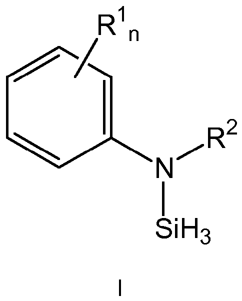
- According to a first aspect of the present invention, there is provided an organoaminosilane precursor according to formula I:


- In a second aspect, there is provided a method for forming a silicon-containing film on at least one surface of a substrate by a deposition process selected from a chemical vapor deposition process and an atomic layer deposition process, the method comprising reacting at least one organoaminosilane precursor according to the first aspect with either a nitrogen-containing source, or an oxidizing agent, to form said film on said surface.
- In another aspect, there is provided a method of forming a silicon oxide film via an atomic layer deposition process, the method comprising the steps of:
- a. providing a substrate in a reactor;
- b. introducing into the reactor an at least one silicon precursor selected from an at least one organoaminosilane precursor according to the first aspect;
- c. purging the reactor with a purge gas;
- d. introducing an oxygen source into the reactor;
- e. purging the reactor with a purge gas; and
- f. repeating the steps b through e until a desired thickness of the film is obtained.
- In a further aspect, there is provided a method of forming a silicon oxide film onto at least a surface of a substrate using a CVD process comprising:
- a. providing a substrate in a reactor;
- b. introducing into the reactor an at least one organoaminosilane precursor according to the first aspect; and
- c. providing an oxygen source to deposit the silicon oxide film onto the at least one surface.
- In another aspect, there is provided a method of forming a silicon nitride film via an atomic layer deposition process, the method comprising the steps of:
- a. providing a substrate in a reactor;
- b. introducing into the reactor an at least one silicon precursor according to the first aspect;
- c. purging the reactor with a purge gas;
- d. introducing a nitrogen-containing source into the reactor;
- e. purging the reactor with a purge gas; and
- f. repeating the steps b through e until a desired thickness of the silicon nitride film is obtained.
- In a further aspect, there is provided a method of forming a silicon nitride film onto at least a surface of a substrate using a CVD process comprising:
- a. providing a substrate in a reactor;
- b. introducing into the reactor an at least one organoaminosilane precursor according to the first aspect;
- c. providing a nitrogen-containing source wherein the at least one organoaminosilane precursors and the nitrogen-containing source react to deposit the film comprising both silicon and nitrogen onto the at least one surface.
- In another aspect, a vessel for depositing a dielectric film comprising one or more organoaminosilane precursor having Formula I is described herein. In one particular embodiment, the vessel comprises at least one pressurizable vessel (preferably of stainless steel) fitted with the proper valves and fittings to allow the delivery of one or more precursors to the reactor for a CVD or an ALD process.
- Organoaminosilanes, silane, or silicon-containing precursors are used as precursors to form stoichiometric and non-stoichiometric silicon containing films such as, but not limited to, silicon oxide, silicon oxycarbide, silicon nitride, silicon oxynitride and silicon oxycarbonitride. These precursors can also be used, for example, as dopants for metal containing films. The organoaminosilane precursors are typically high purity volatile liquid precursor chemical that are vaporized and delivered to a deposition chamber or reactor as a gas to deposit a silicon containing film via CVD or ALD processes for semiconductor devices. The selection of precursor materials for deposition depends upon the desired resultant dielectric material or film. For example, a precursor material may be chosen for its content of chemical elements, its stoichiometric ratios of the chemical elements, and/or the resultant dielectric film or coating that are formed under CVD. The precursor material may also be chosen for various other characteristics such as cost, non-toxicity, handling characteristics, ability to maintain liquid phase at room temperature, volatility, molecular weight, and/or other considerations. In certain embodiments, the precursors described herein can be delivered to the reactor system by any number of means, preferably using a pressurizable stainless steel vessel fitted with the proper valves and fittings, to allow the delivery of liquid phase precursor to the deposition chamber or reactor.
- The organoaminosilanes precursors described herein exhibit a balance of reactivity and stability that makes them ideally suitable as CVD or ALD precursors. With regard to reactivity, certain precursors may have boiling points that are too high to be vaporized and delivered to the reactor to be deposited as a film on a substrate. Precursors having higher relative boiling points require that the delivery container and lines need to be heated at or above the boiling point of the precursor to prevent condensation or particles from forming in the container, lines, or both. With regard to stability, other precursors may form silane (SiH4) as they degrade. Silane is pyrophoric at room temperature or it can spontaneously combust which presents safety and handling issues. Moreover, the formation of silane and other by-products decreases the purity level of the precursor and changes as small as 1-2% in chemical purity may be considered unacceptable for reliable semiconductor manufacture. In certain embodiments, the organoaminosilane precursors having formula I comprise less than 2% by weight, or less than 1% by weight, or less than 0.5% by weight of by-product (such as the corresponding bis-silane byproduct) after being stored for a period of time of 6 months or more, or one year or more. In addition to the foregoing advantages, in certain embodiments such as for depositing a silicon oxide or silicon nitride film using an ALD or plasma-enahnced atomic layer deposition ("PEALD") deposition method, the organoaminosilane precursor described herein may be able to deposit high density materials at relatively low deposition temperatures, e.g., at 500°C or less, at 400°C or less, or at 300°C or less. In one particular embodiment, the organoaminosilane precursor, such as phenylmethylaminosilane, can be used to deposit a dielectric film via ALD or PEALD at a temperature as low as 50°C or less, or at room temperature (e.g., 25°C).
- In one aspect, there is provided certain precursors or organoaminosilanes that are represented by the following formula I:
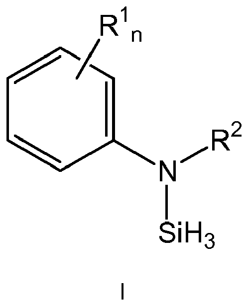
- In formula I and throughout the description, the term "alkyl" denotes a linear, or branched functional group having from 1 to 20, e.g. 1 to 12 or 1 to 6, carbon atoms.
- Exemplary alkyl groups include, but are not limited to, methyl, ethyl, propyl, isopropyl, butyl, isobutyl, sec-butyl, tert-butyl, pentyl, iso-pentyl, tert-pentyl, hexyl, isohexyl, and neohexyl. In certain embodiments, the alkyl group may have one or more functional groups such as, but not limited to, an alkoxy group, a dialkylamino group or combinations thereof, or an electron withdrawing group, e.g. a nitrile group attached thereto. In other embodiments, the alkyl group does not have one or more functional groups attached thereto.
- In formula I and throughout the description, the term "cyclic alkyl" denotes a cyclic functional group having from 3 to 12, e.g. from 4 to 10, carbon atoms. Exemplary cyclic alkyl groups include, but are not limited to, cyclobutyl, cyclopentyl, cyclohexyl, and cyclooctyl groups.
- In formula I and throughout the description, the term "aryl" denotes an aromatic cyclic functional group having from 5 to 12 carbon atoms, or from 6 to 10 carbon atoms. Exemplary aryl groups include, but are not limited to, phenyl, benzyl, chlorobenzyl, tolyl, and o-xylyl.
- In formula I and throughout the description, the term "alkenyl group" denotes a group which has one or more carbon-carbon double bonds and has from 2 to 20, e.g. from 2 to 12 or from 2 to 6, carbon atoms.
- In formula I and throughout the description, the term "alkynyl group" denotes a group which has one or more carbon-carbon triple bonds and has from 2 to 20, e.g. from 2 to 12 or from 2 to 6, carbon atoms.
- In formula I and throughout the description, the term "alkoxy" denotes an alkyl group which is linked to an oxygen atom (e.g., R-O) and may have from 1 to 20, e.g. from 1 to 12 or from 1 to 6, carbon atoms. Exemplary alkoxy groups include, but are not limited to, methoxy (-OCH3), ethoxy (-OCH2CH3), n-propoxy (-OCH2CH2CH3), and iso-propoxy (-OCHMe2).
- In formula I and throughout the description, the term "dialkylamine group" denotes a group which has two alkyl groups attached to a nitrogen atom and has from 2 to 20, e.g. from 2 to 12 or from 2 to 6, carbon atoms.
- The term "electron withdrawing substituent" as used herein describes an atom or group thereof that acts to draw electrons away from the Si-N bond. Examples of suitable electron withdrawing substituents include, but are not limited to, halogens (F, Cl, Br, I) and nitriles (CN). In certain embodiments, electron withdrawing substituent can be adjacent to or proximal to N in formula I. Further non-limiting examples of an electron withdrawing group includes F, Cl, Br, I, CN, NO2, RSO, and/or RSO2 wherein R can be a C1 to C10 alkyl group such as, but not limited to, a methyl group or another group.
- In certain embodiments, one or more of the alkyl group, alkenyl group, alkynyl group, alkoxy group, dialkylamino group, aryl group, and/or electron withdrawing group in formula I (and II - see below) may be substituted or have one or more atoms or group of atoms substituted in place of, for example, a hydrogen atom. Exemplary substituents include, but are not limited to, oxygen, sulfur, halogen atoms (e.g., F, Cl, I, or Br), nitrile, nitrogen, and phosphorous. In other embodiments, one or more of the alkyl group, alkenyl group, alkynyl group, alkoxy group, dialkylamino aryl group, and/or electron withdrawing group in Formula I and II may be unsubstituted.
- In certain embodiments, substituents R1 and R2 are linked in formula I to form a ring structure. In other embodiments, substituent R1 and R2 are not linked in formula I.
- In certain embodiments wherein n in formula I is a number greater than 1, R1 is the same. An example of this can be an embodiment wherein n is 2 and the two R1 substituents are both methyl groups. In other embodiments wherein n in formula I is a number greater than 1, R1 is different. An example of this can be an embodiment wherein n is 2 and the two R1 substituents are a methyl group and a Cl atom. In these or other embodiments, R1 and R2 are independent of each other. In alternative embodiments wherein n in formula I is a number greater than 1, one of substituents R1 and R2 are linked in formula I to form a ring structure.
- In certain embodiments, the at least one organoaminosilane precursor having formula I has one or more substituents comprising oxygen atoms. In these embodiments, the need for an oxygen source during the deposition process may be avoided. In other embodiments, the at least one organoaminosilane precursor having formula I has one or more substituents comprising oxygen atoms also uses an oxygen source. In this or other embodiments, substituents R1 and R2 are linked via an oxygen atom in formula I to form a ring structure. The following Table 1 provides some non-limiting examples of certain embodiments of the organoaminosilanes having formula I.

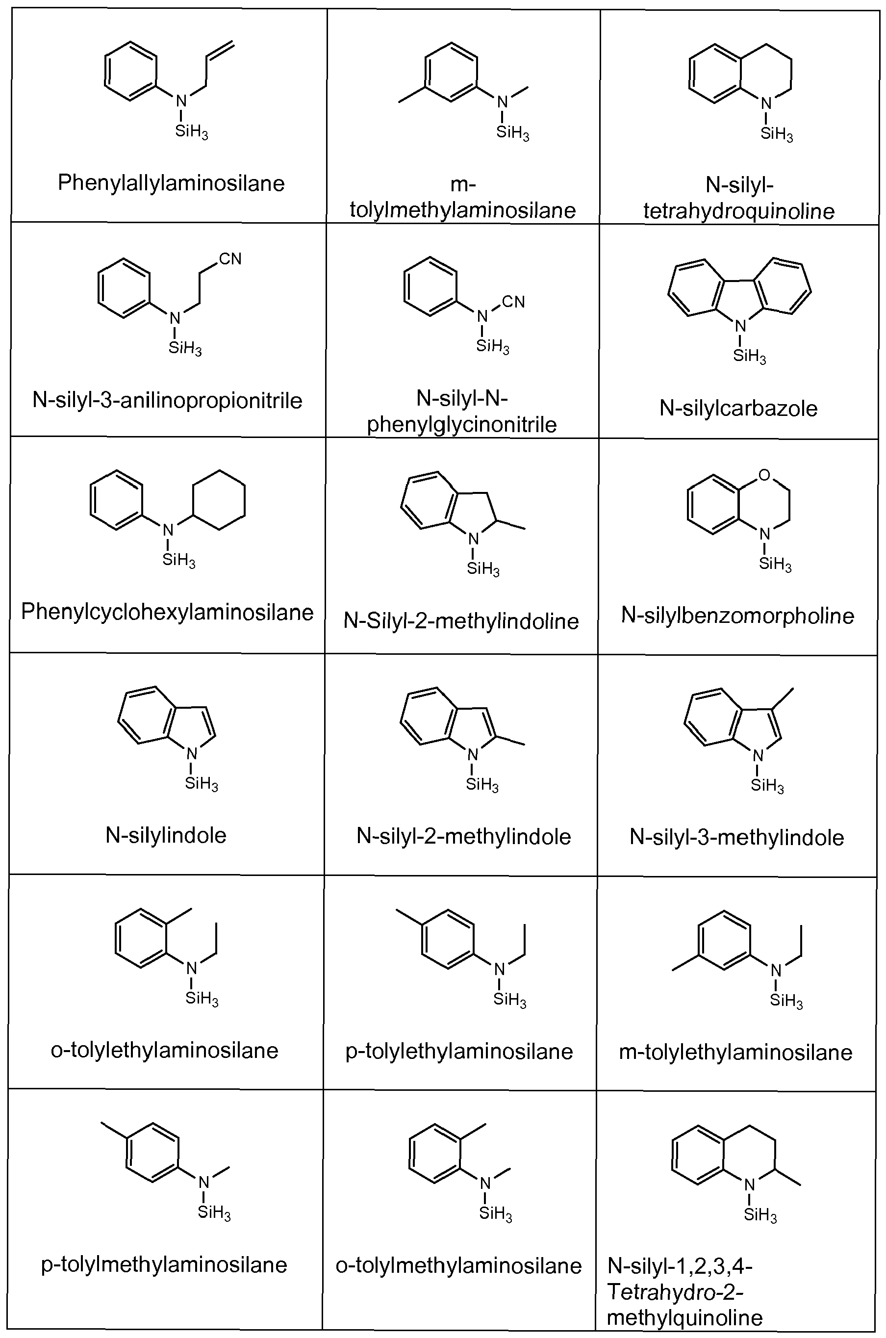
- Without being bound by theory, it is believed that organoaminosilane precursors such as those organoaminosilanes having formula I described herein and having a -SiH3 group are advantageous over other organoaminosilane precursors containing SiH2 or -SiH groups because of its lower activation barrier to react on a hydroxylated semi-conductor surface (thus lower deposition temperature), lower impurity and higher film density after deposition. However, certain organoaminosilane precursors having a -SiH3 group such as dimethylaminosilane (DMAS) or diethylaminosilane (DEAS) may not be thermally stable because it undergoes a disproportionational reaction to form pyrophoric silane and bis(dimethylamino)silane or bis(diethylamino)silane, respectively. It has been found that the activation barrier for PMAS was relatively low compared with DMAS. Further, it is thought that films deposited using these particular organoaminosilane precursors may contain appropriate levels and types of carbon in silicon nitride or silicon carbonitride networks that may enable a significant reduction in wet etch rate yet maintaining a certain dielectric constant value. In addition, it has also been found that the present organoaminosilane precursors having Formula I described herein may allow for lower temperature depositions, such as, for example, room temperature depositions, than other organoaminosilanes known in the art such as diispropylaminosilane.
- In certain embodiments, the organoaminosilanes having formula I can be prepared by reacting a monochlorosilane (MCS) or lower molecular dialkylaminosilane such as di-iso-propylaminosilane with an amine having the following Formula II in an organic solvent or solvent mixture.

- In formula II, R1, R2 and n are as defined above. Exemplary amines having formula II wherein R1 is hydrogen, a linear or branched C1 to C6 alkyl group, halide and R2 is a linear or branched C1 to C6 alkyl group or a C4 to C10 cyclic alkyl include, but are not limited to, N-methylaniline, N-ethylaniline, N-iso-propylaniline, n-Butylaniline , N-allylaniline, N-Ethyl-m-toluidine, N-Methyl-o-toluidine, N-Methyl-p-toluidine, 4-fluoro-N-methylaniline, 4-Chloro-N-methylaniline, N-cyclohexylaniline, 3-anilinopropionitrile, or N-phenylglycinonitrile. Exemplary amines having formula II wherein R1 and R2 are linked to form a ring include, but are not limited to, 3-methylindole, 2-methylindole, indole, tetrahydroquinoline, 8-methyl-1,2,3,4-tetrahydroquinoline, 3-indoleacetonitrile, 2-methylindoline, 2,3-dihydroindole, 5-methylindoline, 1,2,3,4-tetrahydroquinoline, 1,2,3,4-tetrahydro-2-methylquinoline, 1,2,3,4-tetrahydro-6-methylquinoline, 3,4-dihydro-2H-1,4-benzoxazine, carbazole, and 3,6-dibromocarbazole.
- The following
Equations 1 through 3 provide examples of reaction schemes or synthesis routes which may be used to make the organoaminosilanes having formula I as described herein.Reaction schemes 1 through 3 can be conducted with (e.g., in the presence of) or without (e.g., in the absence of) organic solvents. In embodiments wherein an organic solvent is used, examples of suitable organic solvents include, but are not limited to, hydrocarbon such as hexanes, octane, toluene, and ethers such as diethylether, and tetrahydrofuran (THF). In these or other embodiments, the reaction temperature is in the range of from about -70°C to the boiling point of the solvent employed if a solvent is involved. The resulting organoaminosilane can be purified via vacuum distillation after removing all by-products as well as solvent(s) if present.Equation 1 is an embodiment involving a silyl exchange reaction. An example of this synthetic route is provided herein as Example 1.Equation 2 is an embodiment wherein a chlorinated silane is used as a reagent. An example of this synthetic route is provided herein as Example 2. Equation 3 is an embodiment wherein a metal amide such as a lithium or potassium amide and a chlorinated silane are used as reagents and results in the desired end product and a metal halide by-product.


- The method used to form the silicon-containing dielectric films or coatings are deposition processes. Examples of suitable deposition processes for the method disclosed herein include, but are not limited to, cyclic CVD (CCVD), MOCVD (Metal Organic CVD), thermal chemical vapor deposition, plasma enhanced chemical vapor deposition ("PECVD"), high density PECVD, photon assisted CVD, plasma-photon assisted ("PPECVD"), cryogenic chemical vapor deposition, chemical assisted vapor deposition, hot-filament chemical vapor deposition, CVD of a liquid polymer precursor, deposition from supercritical fluids, and low energy CVD (LECVD). In certain embodiments, the metal containing films are deposited via atomic layer deposition (ALD), plasma enhanced ALD (PEALD) or plasma enhanced cyclic CVD (PECCVD) process. As used herein, the term "chemical vapor deposition processes" refers to any process wherein a substrate is exposed to one or more volatile precursors, which react and/or decompose on the substrate surface to produce the desired deposition. As used herein, the term "atomic layer deposition process" refers to a self-limiting (e.g., the amount of film material deposited in each reaction cycle is constant), sequential surface chemistry that deposits films of materials onto substrates of varying compositions. Although the precursors, reagents and sources used herein may be sometimes described as "gaseous", it is understood that the precursors can be either liquid or solid which are transported with or without an inert gas into the reactor via direct vaporization, bubbling or sublimation. In some case, the vaporized precursors can pass through a plasma generator. In one embodiment, the dielectric film is deposited using an ALD process. In another embodiment, the dielectric film is deposited using a CCVD process. In a further embodiment, the dielectric film is deposited using a thermal CVD process. The term "reactor" as used herein, includes without limitation, reaction chamber or deposition chamber.
- In certain embodiments, the method disclosed herein avoids pre-reaction of the precursors by using ALD or CCVD methods that separate the precursors prior to and/or during the introduction to the reactor. In this connection, deposition techniques such as ALD or CCVD processes are used to deposit the dielectric film. In one embodiment, the film is deposited via an ALD process by exposing the substrate surface alternatively to the one or more the silicon-containing precursor, oxygen source, nitrogen-containing source, or other precursor or reagent. Film growth proceeds by self-limiting control of surface reaction, the pulse length of each precursor or reagent, and the deposition temperature. However, once the surface of the substrate is saturated, the film growth ceases.
- In certain embodiments, the method described herein further comprises one or more additional silicon-containing precursors other than the organoaminosilane precursor having the above formula I. Examples of additional silicon-containing precursors include, but are not limited to, organo-silicon compounds such as siloxanes (e.g., hexamethyl disiloxane (HMDSO) and dimethyl siloxane (DMSO)); organosilanes (e.g., methylsilane; dimethylsilane; vinyl trimethylsilane; trimethylsilane; tetramethylsilane; ethylsilane; disilylmethane; 2,4-disilapentane; 1,4-disilabutane; 2,5-disilahexane; 2,2-disilylpropane; 1,3,5-trisilacyclohexane, and fluorinated derivatives of these compounds; phenyl-containing organo-silicon compounds (e.g., dimethylphenylsilane and diphenylmethylsilane); oxygen-containing organo-silicon compounds ,e.g., dimethyldimethoxysilane; 1,3,5,7-tetramethylcyclotetrasiloxane; 1,1,3,3-tetramethyldisiloxane; 1,3,5,7-tetrasila-4-oxo-heptane; 2,4,6,8-tetrasila-3,7-dioxo-nonane; 2,2-dimethyl-2,4,6,8-tetrasila-3,7-dioxo-nonane; octamethylcyclotetrasiloxane; [1,3,5,7,9]-pentamethylcyclopentasiloxane; 1,3,5,7-tetrasila-2,6-dioxo-cyclooctane; hexamethylcyclotrisiloxane; 1,3-dimethyldisiloxane; 1,3,5,7,9-pentamethylcyclopentasiloxane; hexamethoxydisiloxane, and fluorinated derivatives of these compounds.
- Depending upon the deposition method, in certain embodiments, the one or more silicon-containing precursors may be introduced into the reactor at a predetermined molar volume, or from about 0.1 to about 1000 micromoles. In this or other embodiments, the silicon-containing and/or organoaminosilane precursor may be introduced into the reactor for a predetermined time period. In certain embodiments, the time period ranges from about 0.001 to about 500 seconds.
- In certain embodiments, the dielectric films deposited using the methods described herein are formed in the presence of oxygen using an oxygen source, reagent or precursor comprising oxygen. An oxygen source may be introduced into the reactor in the form of at least one oxygen source and/or may be present incidentally in the other precursors used in the deposition process. Suitable oxygen source gases may include, for example, water (H2O) (e.g., deionized water, purified water, and/or distilled water), oxygen (O2), oxygen plasma, ozone (O3), NO, NO2, carbon monoxide (CO), carbon dioxide (CO2) and combinations thereof. In certain embodiments, the oxygen source comprises an oxygen source gas that is introduced into the reactor at a flow rate ranging from about 1 to about 2000 square cubic centimeters (sccm) or from about 1 to about 1000 sccm. The oxygen source can be introduced for a time that ranges from about 0.1 to about 100 seconds. In one particular embodiment, the oxygen source comprises water having a temperature of 10°C or greater. In embodiments wherein the film is deposited by an ALD or a cyclic CVD process, the precursor pulse can have a pulse duration that is greater than 0.01 seconds, and the oxygen source can have a pulse duration that is less than 0.01 seconds, while the water pulse duration can have a pulse duration that is less than 0.01 seconds. In yet another embodiment, the purge duration between the pulses that can be as low as 0 seconds or is continuously pulsed without a purge in-between. The oxygen source or reagent is provided in a molecular amount less than a 1:1 ratio to the silicon precursor, so that at least some carbon is retained in the as deposited dielectric film.
- In certain embodiments, the dielectric films comprise silicon and nitrogen. In these embodiments, the dielectric films deposited using the methods described herein are formed in the presence of nitrogen-containing source. An nitrogen-containing source may be introduced into the reactor in the form of at least one nitrogen source and/or may be present incidentally in the other precursors used in the deposition process. Suitable nitrogen-containing source gases may include, for example, ammonia, hydrazine, monoalkylhydrazine, dialkylhydrazine, nitrogen, nitrogen/hydrogen, ammonia plasma, nitrogen plasma, nitrogen/hydrogen plasma, and mixture thereof. In certain embodiments, the nitrogen-containing source comprises an ammonia plasma or hydrogen/nitrogen plasma source gas that is introduced into the reactor at a flow rate ranging from about 1 to about 2000 square cubic centimeters (sccm) or from about 1 to about 1000 sccm. The nitrogen-containing source can be introduced for a time that ranges from about 0.1 to about 100 seconds. In embodiments wherein the film is deposited by an ALD or a cyclic CVD process, the precursor pulse can have a pulse duration that is greater than 0.01 seconds, and the nitrogen-containing source can have a pulse duration that is less than 0.01 seconds, while the water pulse duration can have a pulse duration that is less than 0.01 seconds. In yet another embodiment, the purge duration between the pulses that can be as low as 0 seconds or is continuously pulsed without a purge in-between.
- The deposition methods disclosed herein may involve one or more purge gases. The purge gas, which is used to purge away unconsumed reactants and/or reaction byproducts, is an inert gas that does not react with the precursors. Exemplary purge gases include, but are not limited to, argon (Ar), nitrogen (N2), helium (He), neon (Ne), hydrogen (H2), and mixtures thereof. In certain embodiments, a purge gas such as Ar is supplied into the reactor at a flow rate ranging from about 10 to about 2000 sccm for about 0.1 to 1000 seconds, thereby purging the unreacted material and any byproduct that may remain in the reactor.
- The respective step of supplying the precursors, oxygen source, the nitrogen-containing source, and/or other precursors, source gases, and/or reagents may be performed by changing the time for supplying them to change the stoichiometric composition of the resulting dielectric film.
- Energy is applied to the at least one of the precursor, nitrogen-containing source, reducing agent, other precursors or combination thereof to induce reaction and to form the dielectric film or coating on the substrate. Such energy can be provided by, but not limited to, thermal, plasma, pulsed plasma, helicon plasma, high density plasma, inductively coupled plasma, X-ray, e-beam, photon, remote plasma methods, and combinations thereof. In certain embodiments, a secondary RF frequency source can be used to modify the plasma characteristics at the substrate surface. In embodiments wherein the deposition involves plasma, the plasma-generated process may comprise a direct plasma-generated process in which plasma is directly generated in the reactor, or alternatively a remote plasma-generated process in which plasma is generated outside of the reactor and supplied into the reactor.
- The organoaminosilane precursors and/or other silicon-containing precursors may be delivered to the reaction chamber such as a CVD or ALD reactor in a variety of ways. In one embodiment, a liquid delivery system may be utilized. In an alternative embodiment, a combined liquid delivery and flash vaporization process unit may be employed, such as, for example, the turbo vaporizer manufactured by MSP Corporation of Shoreview, MN, to enable low volatility materials to be volumetrically delivered, which leads to reproducible transport and deposition without thermal decomposition of the precursor. In liquid delivery formulations, the precursors described herein may be delivered in neat liquid form, or alternatively, may be employed in solvent formulations or compositions comprising same. Thus, in certain embodiments the precursor formulations may include solvent component(s) of suitable character as may be desirable and advantageous in a given end use application to form a film on a substrate.
- In another embodiment, a vessel for depositing a dielectric film comprising one or more organoaminosilane precursor having formula I is described herein. In one particular embodiment, the vessel comprises at least one pressurizable vessel (preferably of stainless steel) fitted with the proper valves and fittings to allow the delivery of one or more precursors to the reactor for a CVD or an ALD process. In this or other embodiments, the organoaminosilane precursor of Formula I is provided in a pressurizable vessel comprised of stainless steel and the purity of the precursor is 98% by weight or greater or 99.5% or greater which is suitable for the majority of semiconductor applications. In certain embodiments, such vessels can also have means for mixing the precursors with one or more additional precursor if desired. In these or other embodiments, the contents of the vessel(s) can be premixed with an additional precursor. Alternatively, the organoaminosilane precursor and/or other precursor can be maintained in separate vessels or in a single vessel having separation means for maintaining the organoaminosilane precursor and other precursor separate during storage.
- In one embodiment of the method described herein, a cyclic deposition process such as CCVD, ALD, or PEALD may be employed, wherein at least one silicon-containing precursor selected from an organoaminosilane precursor having Formula I and optionally a nitrogen-containing source such as, for example, ammonia, hydrazine, monoalkylhydrazine, dialkylhydrazine, nitrogen, nitrogen/hydrogen, ammonia plasma, nitrogen plasma, nitrogen/hydrogen plasma are employed.
- In certain embodiments, the gas lines connecting from the precursor canisters to the reaction chamber are heated to one or more temperatures depending upon the process requirements and the container of the organoaminosilane precursor having Formula I is kept at one or more temperatures for bubbling. In other embodiments, a solution comprising the at least one silicon-containing precursor having Formula I is injected into a vaporizer kept at one or more temperatures for direct liquid injection.
- A flow of argon and/or other gas may be employed as a carrier gas to help deliver the vapor of the at least one organoaminosilane precursor to the reaction chamber during the precursor pulsing. In certain embodiments, the reaction chamber process pressure is about 1 Torr (∼133 Pa).
- In a typical ALD or CCVD process, the substrate such as a silicon oxide substrate is heated on a heater stage in a reaction chamber that is exposed to the silicon-containing precursor initially to allow the complex to chemically adsorb onto the surface of the substrate.
- A purge gas such as argon purges away unabsorbed excess complex from the process chamber. After sufficient purging, a nitrogen-containing source may be introduced into reaction chamber to react with the absorbed surface followed by another gas purge to remove reaction by-products from the chamber. The process cycle can be repeated to achieve the desired film thickness.
- In this or other embodiments, it is understood that the steps of the methods described herein may be performed in a variety of orders, may be performed sequentially or concurrently (e.g., during at least a portion of another step), and any combination thereof. The respective step of supplying the precursors and the nitrogen-containing source gases may be performed by varying the duration of the time for supplying them to change the stoichiometric composition of the resulting dielectric film.
- In another embodiment of the method disclosed herein, the films containing both silicon and nitrogen are formed using a ALD deposition method that comprises the steps of:
- providing a substrate in an ALD reactor;
- introducing into the ALD reactor an at least one organoaminosilane precursor comprising a precursor according to formula I as defined above;
- chemisorbing the at least one organoaminosilane precursor onto a substrate;
- purging away the unreacted at least one organoaminosilane precursor using a purge gas;
- providing a nitrogen-containing source to the organoaminosilane precursor onto the heated substrate to react with the sorbed at least one organoaminosilane precursor; and
- optionally purging away any unreacted nitrogen-containing source.
- In another embodiment of the method disclosed herein, the dielectric films is formed using a ALD deposition method that comprises the steps of:
- providing a substrate in a reactor;
- introducing into the reactor an at least one organoaminosilane precursor according to formula I as defined above;
- chemisorbing the at least one organoaminosilane precursor onto a substrate;
- purging away the unreacted at least one organoaminosilane precursor using a purge gas;
- providing an oxygen source to the organoaminosilane precursor onto the heated substrate to react with the sorbed at least one organoaminosilane precursor; and
- optionally purging away any unreacted oxygen source.
- The above steps define one cycle for the method described herein; and the cycle can be repeated until the desired thickness of a dielectric film is obtained. In this or other embodiments, it is understood that the steps of the methods described herein may be performed in a variety of orders, may be performed sequentially or concurrently (e.g., during at least a portion of another step), and any combination thereof. The respective step of supplying the precursors and oxygen source may be performed by varying the duration of the time for supplying them to change the stoichiometric composition of the resulting dielectric film, although always using oxygen in less than a stoichiometric amount relative to the available silicon.
- For multi-component dielectric films, other precursors such as silicon-containing precursors, nitrogen-containing precursors, reducing agents, or other reagents can be alternately introduced into the reactor chamber.
- In a further embodiment of the method described herein, the dielectric film is deposited using a thermal CVD process. In this embodiment, the method comprises:
- placing one or more substrates into a reactor which is heated to a temperature ranging from ambient temperature to about 700°C and maintained at a pressure of 1 Torr (133 Pa) or less;
- introducing at least one organoaminosilane precursor according to formula I as defined above; and
- providing an oxygen source into the reactor to at least partially react with the at least one organoaminosilane precursor and deposit a dielectric film onto the one or more substrates. In certain embodiments of the CVD method, the reactor is maintained at a pressure ranging from 100 mTorr to 600 mTorr (13 to 80 Pa) during the introducing step.
- The above steps define one cycle for the method described herein; and the cycle can be repeated until the desired thickness of a dielectric film is obtained. In this or other embodiments, it is understood that the steps of the methods described herein may be performed in a variety of orders, may be performed sequentially or concurrently (e.g., during at least a portion of another step), and any combination thereof. The respective step of supplying the precursors and oxygen source may be performed by varying the duration of the time for supplying them to change the stoichiometric composition of the resulting dielectric film, although always using oxygen in less than a stoichiometric amount relative to the available silicon.
- For multi-component dielectric films, other precursors such as silicon-containing precursors, nitrogen-containing precursors, oxygen sources, reducing agents, and/or other reagents can be alternately introduced into the reactor chamber.
- In a further embodiment of the method described herein, the dielectric film is deposited using a thermal CVD process. In this embodiment, the method comprises:
- placing one or more substrates into a reactor which is heated to a temperature ranging from ambient temperature to about 700°C and maintained at a pressure of 1 Torr (133 Pa) or less;
- introducing at least one organoaminosilane precursor according to formula I defined above; and
- providing a nitrogen-containing source into the reactor to at least partially react with the at least one organoaminosilane precursor and deposit a dielectric film onto the one or more substrates. In certain embodiments of the CVD method, the reactor is maintained at a pressure ranging from 100 mTorr to 600 mTorr (13 to 80 Pa) during the introducing step.
- In certain embodiments, the organoaminosilane precursors having Formula I described herein can also be used a dopant for metal containing films, such as but not limited to, metal oxide films or metal nitride films. In these embodiments, the metal containing film is deposited using an ALD or CVD process such as those processes described herein using metal alkoxide, metal amide, or volatile organometallic precursors. Examples of suitable metal alkoxide precursors that may be used with the method disclosed herein include, but are not limited to, group 3 to 6 metal alkoxide, group 3 to 6 metal complexes having both alkoxy and alkyl substituted cyclopentadienyl ligands, group 3 to 6 metal complexes having both alkoxy and alkyl substituted pyrrolyl ligands, group 3 to 6 metal complexes having both alkoxy and diketonate ligands; group 3 to 6 metal complexes having both alkoxy and ketoester ligands; Examples of suitable metal amide precursors that may be used with the method disclosed herein include, but are not limited to, tetrakis(dimethylamino)zirconium (TDMAZ), tetrakis(diethylamino)zirconium (TDEAZ), tetrakis(ethylmethylamino)zirconium (TEMAZ), tetrakis(dimethylamino)hafnium (TDMAH), tetrakis(diethylamino)hafnium (TDEAH), and tetrakis(ethylmethylamino)hafnium (TEMAH), tetrakis(dimethylamino)titanium (TDMAT), tetrakis(diethylamino)titanium (TDEAT), tetrakis(ethylmethylamino)titanium (TEMAT), tert-butylimino tri(diethylamino)tantalum (TBTDET), tert-butylimino tri(dimethylamino)tantalum (TBTDMT), tert-butylimino tri(ethylmethylamino)tantalum (TBTEMT), ethylimino tri(diethylamino)tantalum (EITDET), ethylimino tri(dimethylamino)tantalum (EITDMT), ethylimino tri(ethylmethylamino)tantalum (EITEMT), tert-amylimino tri(dimethylamino)tantalum (TAIMAT), tert-amylimino tri(diethylamino)tantalum, pentakis(dimethylamino)tantalum, tert-amylimino tri(ethylmethylamino)tantalum, bis(tert-butylimino)bis(dimethylamino)tungsten (BTBMW), bis(tert-butylimino)bis(diethylamino)tungsten, bis(tert-butylimino)bis(ethylmethylamino)tungsten, and combinations thereof. Examples of suitable organometallic precursors that may be used with the method disclosed herein include, but are not limited to, group 3 metal cyclopentadienyls or alkyl cyclopentadienyls. Exemplary Group 3 to 6 metal herein include, but not limited to, Y, La, Ce, Pr, Nd, Sm, Eu, Gd, Tb, Dy, Er, Yb, Lu, Ti, Hf, Zr, V, Nb, Ta, Cr, Mo, and W.
- In certain embodiments, the resultant dielectric films or coatings can be exposed to a post-deposition treatment such as, but not limited to, a plasma treatment, chemical treatment, ultraviolet light exposure, electron beam exposure, and/or other treatments to affect one or more properties of the film.
- In certain embodiments, the dielectric films described herein have a dielectric constant of 6 or less. In these or other embodiments, the films can a dielectric constant of about 5 or below, or about 4 or below, or about 3.5 or below. However, it is envisioned that films having other dielectric constants (e.g., higher or lower) can be formed depending upon the desired end-use of the film. An example of the silicon containing or dielectric film that is formed using the organoaminosilane precursors and processes described herein has the formulation SixOyCzNvHw wherein Si ranges from about 10% to about 40%; O ranges from about 0% to about 65%; C ranges from about 0% to about 75% or from about 0% to about 50%; N ranges from about 0% to about 75% or from about 0% to 50%; and H ranges from about 0% to about 50% atomic percent weight % wherein x+y+z+v+w = 100 atomic weight percent, as determined for example, by XPS or other means.
- As mentioned previously, the method described herein may be used to deposit a silicon-containing film on at least a portion of a substrate. Examples of suitable substrates include but are not limited to, silicon, SiO2, Si3N4, OSG, FSG, silicon carbide, hydrogenated silicon carbide, silicon nitride, hydrogenated silicon nitride, silicon carbonitride, hydrogenated silicon carbonitride, boronitride, antireflective coatings, photoresists, organic polymers, porous organic and inorganic materials, metals such as copper and aluminum, and diffusion barrier layers such as but not limited to TiN, Ti(C)N, TaN, Ta(C)N, Ta, W, or WN. The films are compatible with a variety of subsequent processing steps such as, for example, chemical mechanical planarization (CMP) and anisotropic etching processes.
- The deposited films have applications, which include, but are not limited to, computer chips, optical devices, magnetic information storages, coatings on a supporting material or substrate, microelectromechanical systems (MEMS), nanoelectromechanical systems, thin film transistor (TFT), and liquid crystal displays (LCD).
- The following examples illustrate the method for preparing organoaminosilane precursors as well as deposited silicon-containing films described herein and are not intended to limit it in any way.
- Further aspects of the present invention include:
- #1. An organoaminosilane precursor represented by the following formula I:

- #2. The organoaminosilane precursor of #1 wherein the R1 and R2 are linked to together to form a ring.
- #3. The organoaminosilane precursor of #1 wherein R1 and R2 are the same.
- #4. The organoaminosilane precursor of #1 wherein R1 and R2 are different.
- #5. The organoaminosilane precursor of #1 comprising at least one selected from the group consisting of phenylmethylaminosilane, phenylethylaminosilane, phenyl-iso-propylaminosilane, phenylallylaminosilane, m-tolylmethylaminosilane, N-silyl-tetrahydroquinoline, N-silyl-3-anilinopropionitrile, N-silyl-N-phenylglycinonitrile, N-silylcarbazole, phenylcyclohexylaminosilane, N-silyl-2-methylindoline, N-silylbenzomorpholine, N-silylindole, N-silyl-2-methylindole, N-silyl-3-methylindole, o-tolylethylaminosilane, p-tolylethylaminosilane, m-tolylethylaminosilane, p-tolylethylaminosilane, o-tolylethylaminosilane, and N-silyl-1,2,3,4-Tetrahydro-2-methylquinoline.
- #6. The organoaminosilane precursor of #5 comprising phenylmethylaminosilane.
- #7. The organoaminosilane precursor of #5 comprising phenylethylaminosilane.
- #8. The organoaminosilane precursor of #5 comprising m-tolylethylaminosilane.
- #9. A method for forming a dielectric film on at least one surface of a substrate by a deposition process chosen from a chemical vapor deposition process and an atomic layer deposition process, the method comprising:
- providing the at least one surface of the substrate in a reaction chamber;
- introducing at least one organoaminosilane precursor having the following formula I in the reactor:

- introducing a nitrogen-containing source into the reactor wherein the at least one organoaminosilane precursor and the nitrogen-containing source react to the dielectric films on the at least one surface.
- #10. The method of #9 wherein the at least one organoaminosilane precursor is selected from the group consisting of phenylmethylaminosilane, phenylethylaminosilane, phenyl-iso-propylaminosilane, phenylallylaminosilane, m-tolylmethylaminosilane, N-silyl-tetrahydroquinoline, N-silyl-3-anilinopropionitrile, N-silyl-N-phenylglycinonitrile, N-silylcarbazole, phenylcyclohexylaminosilane, N-silyl-2-methylindoline, N-silylbenzomorpholine, N-silylindole, N-silyl-2-methylindole, N-silyl-3-methylindole, o-tolylethylaminosilane, p-tolylethylaminosilane, m-tolylethylaminosilane, p-tolylethylaminosilane, o-tolylethylaminosilane, and N-silyl-1,2,3,4-Tetrahydro-2-methylquinoline.
- #11. The method of #10 wherein the at least one organoaminosilane precursor comprises phenylmethylaminosilane.
- #12. The method of #10 wherein the at least one organoaminosilane precursor comprises phenylethylaminosilane.
- #13. The method of #10 wherein the at least one organoaminosilane precursor comprises m-tolylethylaminosilane.
- #14. The method of #9 wherein the nitrogen-containing source is selected from the group consisting of ammonia, hydrazine, monoalkylhydrazine, dialkylhydrazine, nitrogen, nitrogen/hydrogen, ammonia plasma, nitrogen plasma, nitrogen/hydrogen plasma, and mixtures thereof.
- #15. The method of #9 wherein the dielectric film is selected from the group consisting of silicon nitride and silicon carbonitride.
- #16. A method of forming a dielectric film via an atomic layer deposition (ALD) process, the method comprising the steps of:
- a. providing a substrate in an ALD reactor;
- b. providing in the ALD reactor an at least one organoaminosilane precursor having the following formula I:

- c. purging the ALD reactor with an inert gas;
- d. providing a nitrogen-containing source in the ALD reactor;
- e. purging the ALD reactor with an inert gas; and
- f. repeating the steps b through e until a desired thickness of the dielectric film is obtained.
- #17. The method of #16 wherein the at least one organoaminosilane precursor is selected from the group consisting of phenylmethylaminosilane, phenylethylaminosilane, phenyl-iso-propylaminosilane, phenylallylaminosilane, m-tolylmethylaminosilane, N-silyl-tetrahydroquinoline, N-silyl-3-anilinopropionitrile, N-silyl-N-phenylglycinonitrile, N-silylcarbazole, phenylcyclohexylaminosilane, N-silyl-2-methylindoline, N-silylbenzomorpholine, N-silylindole, N-silyl-2-methylindole, N-silyl-3-methylindole, o-tolylethylaminosilane, p-tolylethylaminosilane, m-tolylethylaminosilane, p-tolylethylaminosilane, o-tolylethylaminosilane, and N-silyl-1,2,3,4-Tetrahydro-2-methylquinoline.
- #18. The method of #17 wherein the at least one organoaminosilane precursor comprises phenylmethylaminosilane.
- #19. The method of #17 wherein the at least one organoaminosilane precursor comprises phenylethylaminosilane.
- #20. The method of #17 wherein the at least one organoaminosilane precursor comprises m-tolylethylaminosilane
- #21. The method of #16 wherein the nitrogen-containing source is selected from the group consisting of ammonia, hydrazine, monoalkylhydrazine, dialkylhydrazine, nitrogen, nitrogen/hydrogen, ammonia plasma, nitrogen plasma, nitrogen/hydrogen plasma, and mixtures thereof.
- #22. The method of #16 wherein the dielectric film is selected from the group consisting of silicon nitride and silicon carbonitride.
- #23. A method of forming a dielectric film onto at least a surface of a substrate using a plasma enhanced atomic layer deposition (PEALD) process, the method comprising:
- a. providing a substrate in an ALD reactor;
- b. providing in the ALD reactor an at least one organoaminosilane precursor having the following formula I:

- c. purging the ALD reactor with an inert gas;
- d. providing a plasma nitrogen-containing source in the ALD reactor;
- e. purging the ALD reactor with an inert gas; and
- f. repeating the steps b through e until a desired thickness of the dielectric film is obtained.
- #24. The method of #23 wherein the at least one organoaminosilane precursor is selected from the group consisting of phenylmethylaminosilane, phenylethylaminosilane, phenyl-iso-propylaminosilane, phenylallylaminosilane, m-tolylmethylaminosilane, N-silyl-tetrahydroquinoline, N-silyl-3-anilinopropionitrile, N-silyl-N-phenylglycinonitrile, N-silylcarbazole, phenylcyclohexylaminosilane, N-silyl-2-methylindoline, N-silylbenzomorpholine, N-silylindole, N-silyl-2-methylindole, N-silyl-3-methylindole, o-tolylethylaminosilane, p-tolylethylaminosilane, m-tolylethylaminosilane, p-tolylethylaminosilane, o-tolylethylaminosilane, N-silyl-1,2,3,4-Tetrahydro-2-methylquinoline,.
- #25. The method of #24 wherein the at least one organoaminosilane precursor comprises phenylmethylaminosilane.
- #26. The method of #24 wherein the at least one organoaminosilane precursor comprises phenylethylaminosilane.
- #27. The method of #24 wherein the at least one organoaminosilane precursor comprises m-tolylethylaminosilane
- #28. The method of #23 wherein the nitrogen-containing source is selected from the group consisting of ammonia, hydrazine, monoalkylhydrazine, dialkylhydrazine, nitrogen, nitrogen/hydrogen, ammonia plasma, nitrogen plasma, nitrogen/hydrogen plasma, and mixtures thereof.
- #29. The method of #23 wherein the dielectric film is selected from the group consisting of silicon nitride and silicon carbonitride.
- #30. A method for forming a silicon oxide film on a substrate comprising:
- reacting an oxidizing agent with a precursor comprising an organoaminosilane represented by the following formula I:

- reacting an oxidizing agent with a precursor comprising an organoaminosilane represented by the following formula I:
- #31. The method of #30 wherein the vapor deposition is at least one selected from the group consisting of at least one selected from chemical vapor deposition, low pressure vapor deposition, plasma enhanced chemical vapor deposition, cyclic chemical vapor deposition, plasma enhanced cyclic chemical vapor deposition, atomic layer deposition, and plasma enhanced atomic layer deposition.
- #32. The method of #30 wherein the at least one organoaminosilane precursor is selected from the group consisting of phenylmethylaminosilane, phenylethylaminosilane, phenyl-iso-propylaminosilane, phenylallylaminosilane, m-tolylmethylaminosilane, N-silyl-tetrahydroquinoline, N-silyl-3-anilinopropionitrile, N-silyl-N-phenylglycinonitrile, N-silylcarbazole, phenylcyclohexylaminosilane, N-silyl-2-methylindoline, N-silylbenzomorpholine, N-silylindole, N-silyl-2-methylindole, N-silyl-3-methylindole, o-tolylethylaminosilane, p-tolylethylaminosilane, m-tolylethylaminosilane, p-tolylethylaminosilane, o-tolylethylaminosilane, and N-silyl-1,2,3,4-tetrahydro-2-methylquinoline,
- #33. The method of #30 wherein the reacting step is conducted at a temperature of 200°C or less.
- #34. The method of #30 wherein the reacting step is conducted at a temperature of 100°C or less.
- #35. The method of #30 wherein the reacting step is conducted at 50°C or less.
- #36. A method for forming a silicon oxide film on a substrate comprising:
- forming via vapor deposition of the silicon oxide film on the substrate from a composition comprising at least one organoaminosilane precursor having the following Formula I:

wherein the vapor deposition is at least one selected from chemical vapor deposition, low pressure vapor deposition, plasma enhanced chemical vapor deposition, cyclic chemical vapor deposition, plasma enhanced cyclic chemical vapor deposition, atomic layer deposition, and plasma enhanced atomic layer deposition.
- forming via vapor deposition of the silicon oxide film on the substrate from a composition comprising at least one organoaminosilane precursor having the following Formula I:
- #37. The method of #36 wherein the at least one organoaminosilane precursor is selected from the group consisting of phenylmethylaminosilane, phenylethylaminosilane, phenyl-iso-propylaminosilane, phenylallylaminosilane, m-tolylmethylaminosilane, N-silyl-tetrahydroquinoline, N-silyl-3-anilinopropionitrile, N-silyl-N-phenylglycinonitrile, N-silylcarbazole, phenylcyclohexylaminosilane, N-silyl-2-methylindoline, N-silylbenzomorpholine, N-silylindole, N-silyl-2-methylindole, N-silyl-3-methylindole, o-tolylethylaminosilane, p-tolylethylaminosilane, m-tolylethylaminosilane, p-tolylethylaminosilane, o-tolylethylaminosilane, and N-silyl-1,2,3,4-Tetrahydro-2-methylquinoline.
- #38. The method of #36 wherein the reacting step is conducted at a temperature of 200°C or less.
- #39. The method of #36 wherein the reacting step is conducted at a temperature of 100°C or less.
- #40. The method of #36 wherein the reacting step is conducted at 50°C or less.
- #41. A method for forming a silicon oxide film on a substrate comprising:
- introducing an organoaminosilane represented by the following formula I:

- introducing at least one oxidizing agent into the reactor wherein the at least one oxidizing agent reacts with the organoaminosilane to provide the silicon oxide film on the substrate.
- introducing an organoaminosilane represented by the following formula I:
- #42. A method for forming a silicon oxide film on a substrate wherein the film comprises a thickness, the method comprising:
- a. introducing an at least one organoaminosilane represented by the formula I into a deposition chamber:

- b. chemisorbing the at least one organoaminosilane precursor onto the substrate;
- c. purging away the unreacted at least one organoaminosilane precursor using a purge gas;
- d. providing an oxygen source to the organoaminosilane precursor onto the heated substrate to react with the sorbed at least one organoaminosilaneprecursor; and
- e. optionally purging away any unreacted oxygen source.
- a. introducing an at least one organoaminosilane represented by the formula I into a deposition chamber:
- #43. The method of #42 wherein steps a. through d. and optional step e. are repeated until the thickness of film is established.
- #44. The method of #42 wherein the at least one organoaminosilane precursor is selected from the group consisting of phenylmethylaminosilane, phenylethylaminosilane, phenyl-iso-propylaminosilane, phenylallylaminosilane, m-tolylmethylaminosilane, N-silyl-tetrahydroquinoline, N-silyl-3-anilinopropionitrile, N-silyl-N-phenylglycinonitrile, N-silylcarbazole, phenylcyclohexylaminosilane, N-silyl-2-methylindoline, N-silylbenzomorpholine, N-silylindole, N-silyl-2-methylindole, N-silyl-3-methylindole, o-tolylethylaminosilane, p-tolylethylaminosilane, m-tolylethylaminosilane, p-tolylethylaminosilane, o-tolylethylaminosilane, and N-silyl-1,2,3,4-Tetrahydro-2-methylquinoline.
- #45. The method of #42 wherein the reacting step is conducted at a temperature of 200°C or less.
- #46. The method of #45 wherein the reacting step is conducted at a temperature of 100°C or less.
- #47. The method of #45 wherein the reacting step is conducted at 50°C or less.
- #48. The method of #42 is an atomic layer deposition process.
- #49. The method of #42 is a plasma enhanced cyclic chemical vapor deposition process.
- #50. A vessel which is used to deliver a precursor for the deposition of a silicon-containing film, the vessel comprising:
- the precursor represented by the following formula I:

wherein the purity of the precursor is about 98% or greater. - the precursor represented by the following formula I:
- #51. The vessel of #50 wherein the vessel is comprised of stainless steel.
- The present invention will now be described by way of the following examples and with reference to the drawings, in which:
-
Figure 1 provides the mass spectroscopy (MS) spectra of phenylmethylaminosilane of Example 1; -
Figure 2 provides the mass spectroscopy (MS) spectra of phenylethylaminosilane of Example 3; -
Figure 3 provides the mass spectroscopy (MS) spectra of phenylallylaminosilane of Example 4; -
Figure 4 provides the mass spectroscopy (MS) spectra of N-sillyl-2-methylindoline of Example 5; -
Figure 5 provides the mass spectroscopy (MS) spectra of phenylcyclohexylaminosilane of Example 6; -
Figures 6 (A) and (B) provide the side and top views, respectively of the hydroxylated SiO2 (001) surface used in the computer simulation of Example 7.Figure 6 (C) provides a schematic view of the optimized hydroxylated SiO2 (001) surface wherein O1 and O2 represent two types of surface hydroxyl groups; -
Figure 7 provides the calculated energy profile of minimum energy pathway for deposition of dimethylaminosilane (DMAS) on hydroxylated SiO2(001) surface in the computer simulation presented in Example 7; -
Figure 8 provides the calculated energy profile of minimum energy pathway for deposition of phenylmethylaminosilane (PMAS) on hydroxylated SiO2(001) surface in the computer simulation presented in Example 7; -
Figure 9 provides a comparison of the deposition rate versus temperature for silicon oxide films deposited using either PMAS and diisopropylaminosilane (DIPAS) as the organoaminosilane precursor described in Example 9; -
Figure 10 provides a comparison of the refractive index versus temperature for silicon oxide films deposited using either PMAS and diisopropylaminosilane (DIPAS) as the organoaminosilane precursor described in Example 9; and -
Figure 11 provides a comparison of the stability of various organoaminosilanes precursors, e.g., bistertbutylaminosilane (BTBAS), diethylaminosilane (DEAS), DIPAS, and PMAS, as measured by gas chromatography assay as described in Example 12. - In the following examples, unless stated otherwise, properties were obtained from sample films that were deposited onto medium resistivity (8-12 Ωcm) single crystal silicon wafer substrates.
- In a 500 ml Schlenk flask, 64.2 grams (g) (0.6 mol) N-methylaniline and 131 g (1.0 mol) di-isopropylaminosilane were stirred at ambient temperature under a nitrogen atmosphere for 24 hours. The relatively lower boiling point by-product di-isopropylamine was removed with vacuum at a pressure of 20 mmHg (-2.7 kPa) and room temperature (25°C). The reaction mixture was stirred for another 24 hours. The end-product phenylmethylaminosilane (73.6 g, 89.5% yield) was obtained by vacuum distillation with a boiling point of 60°C at 5 mm Hg (-0.7 kPa). The end-product was characterized by mass spectroscopy (MS) which is provided in
Figure 1 and shows, among other things, peaks at 137, 122, 106, 91, and 77. The molecular weight of the phenylmethylaminosilane was 137.27. - In a 2000ml three-necked flask equipped with a mechanical stirrer, a condenser, and a gas bubbling inlet, 1000 ml hexane, 53.5 g (0.5 mol) N-methylaniline, and 50.5 g (0.5 mol) triethylamine were cooled to - 20°C with stirring under nitrogen atmosphere. Monochlorosilane (MCS) was bubbled through the reaction mixture. A white solid precipitate was formed. After the reaction was complete, the temperature of the reaction mixture was allowed to warm to room temperature while stirring continued for an additional 2 hours at room temperature. Solid triethylamine hydrochloride salt was removed by filtration, and the solvent hexane was removed by distillation. The product phenylmethylaminosilane (51.3g, 75% yield) was obtained by vacuum distillation with boiling point of 60 C at 5 mm Hg (-0.7 kPa). The compound was characterized by mass spectroscopy and confirms that the product is phenylmethylaminosilane. A comparison of Examples 1 and 2 shows that the synthesis method of Example 1 provided a higher product yield and is more convenient in lab scale synthesis.
- In a 500 ml Schlenk flask, 60.5 g (0.5 mol) N-ethylaniline and 131 g (1.0 mol) di-isopropylaminosilane were stirred at ambient temperature under a nitrogen atmosphere for 24 hours. The relatively lower boiling point by-product di-isopropylamine was removed with vacuum at a pressure of 20 mmHg (-2.7 kPa) and room temperature (25°C). The reaction mixture was stirred for another 24 hours. The end-product phenylethylaminosilane was obtained by vacuum distillation. The end-product was characterized by mass spectroscopy (MS) which is provided in
Figure 2 and shows, among other things, peaks at 151, 150, 136, 120, 106, 93, and 77. The molecular weight of the phenylethylaminosilane was 151.28. - In a 500 ml Schlenk flask, 62.5 g (0.5 mol) N-allylaniline and 131 g (1.0 mol) di-isopropylaminosilane were stirred at ambient temperature under a nitrogen atmosphere for 24 hours. The relatively lower boiling point by-product di-isopropylamine was removed with vacuum at a pressure of 20 mmHg (-2.7 kPa) and room temperature (25°C). The reaction mixture was stirred for another 24 hours. The end-product phenylallylaminosilane was obtained by vacuum distillation. The end-product was characterized by mass spectroscopy (MS) which is provided in
Figure 3 and shows, among other things, peaks at 163, 162, 148, 136, 120, 107, 93, and 77. The molecular weight of the phenylallylaminosilane was 163.29. - In a 500 ml Schlenk flask, 62.5 g (0.5 mol) 2-methyindoline and 131 g (1.0 mol) di-isopropylaminosilane were stirred at ambient temperature under a nitrogen atmosphere for 24 hours. The relatively lower boiling point by-product di-isopropylamine was removed with vacuum at a pressure of 20 mmHg (-2.7 kPa) and room temperature (25°C). The reaction mixture was stirred for another 24 hours. The end-product N-silyl-2-methylindoline was obtained by vacuum distillation. The compound was characterized by mass spectroscopy (MS). The end-product was characterized by mass spectroscopy (MS) which is provided in
Figure 4 and shows, among other things, peaks at 163, 162, 148, 132, 117, 105, 91, and 77. The molecular weight of the N-silyl-2-methylindoline was 163.29. - In a 500 ml Schlenk flask 87.5 g (0.6 mol) N-cyclohexylaniline and 131 g (1.0 mol) di-isopropylaminosilane were stirred at ambient temperature under a nitrogen atmosphere for 24 hours. The relatively lower boiling point by-product di-isopropylamine was removed with vacuum at a pressure of 20 mmHg (-2.7 kPa) and room temperature (25°C). The reaction mixture was stirred for another 24 hours. The end-product phenylcyclohexylaminosilane was obtained by vacuum distillation. The end-product was characterized by mass spectroscopy (MS) which is provided in
Figure 5 and shows, among other things, peaks at 205, 178, 162, 132, 115, 93, and 77. The molecular weight of the phenylcyclohexylaminosilane was 205.37. - A quantum mechanical method based on PM3 using SPARTAN06 simulation package (Wavefunction, Inc., Irvine, California) was used to study the relative chemical stability of several precursors against α-H migration and disproportionation reaction. Using quantum mechanical density functional theory, extensive calculations were conducted using computer modeling software to systematically evaluate the reaction energies of various SiN precursors. The calculations were done under the generalized gradient approximation (GGA) using the exchange-correlation functional proposed by Perdew-Wang (PW91) coupled with the double numerical atomic basis set augmented with polarization functions. All molecular structures were fully optimized to obtain the energetically most favorable geometries. The precursors used in the computer analysis are as follows: dimethylaminosilane (DMAS) and the precursor having Formula I described herein or phenylmethylaminosilane (PMAS).
- For this computer simulation, the reconstructed and fully hydroxylated SiO2 (001) surface was modeled with a slab containing 6-layers alternated with two layers of O atoms and one layer of Si atoms, which is the preferred surface orientation for silica (see Figure 1 (A)). The top two layers of O atoms are all terminated by H atoms, representing the fully hydroxylated surface. There is a vacuum between adjacent slabs with 20 A (2 nm) separation. The selected super cell contains 8 Si atoms, 20 O atoms and 8 H atoms, in addition to a precursor molecule. Prior to the precursor deposition, the surface was fully equilibrated. The optimized main structural parameters, shown in Table 2, are in good agreement with the experimental values and previous DFT calculations.
- A simulated atomic layer deposition process to develop a SiO2 film using a Si precursor takes two successive steps. In the first step, a silicon precursor is vaporized and then introduced onto a hydroxylated Si surface. Subsequently, reaction occurs on the surface with Si attacking the surface O on the hydroxyl group and the H of the hydroxyl group attacks the amino group of the precursor. The reaction leads to formation of a surface Si-O bond and liberation of an amine molecule into the gas-phase. In the second step, an oxygen source such as O3 or O2 molecules are introduced to oxidize the Si-H bonds. These steps would lead to growth of one layer of SiO2 film. The oxidation step is kinetically very fast and highly exothermic. Therefore, one important step to consider in the ALD process is Si precursor deposition. Different precursors give rise to very different quality of SiO2 films.
- The first principles DFT calculations were performed to investigate the minimum energy pathway of DMAS deposition on the fully hydroxylated SiO2(001) surface. The calculated energy profile is shown in
Figure 7 . The simulation yields a thermochemical energy of-15.1 kcal/mol and activation barrier of 11.5 kcal/mol. The results suggest that DMAS is a reactive precursor and can be deposited on the surface with favorable thermodynamics and a low activation barrier. However, DMAS is not thermally stable and can readily undergo the following disproportionational reaction at ambient conditions:
2 (CH3)2NSiH3 →(CH3)2NSiH2N(CH3)2 + SiH4
The calculated thermochemical energy and activation barrier for this reaction are -0.6 kcal/mol and 5.4 kcal/mol, respectively. While the reaction is essentially thermochemically neutral, the exceedingly low activation barrier promotes the disproportionational reaction at room temperature, indicating DMAS is not stable. - The first principles DFT calculations were performed to investigate the minimum energy pathway of PMAS deposition on the fully hydroxylated SiO2(001) surface. The calculated energy profile is shown in
Fig. 8 . The simulation yields a thermochemical energy of -16.9 kcal/mol and activation barrier of 14.1 kcal/mol. The results suggest that PMAS has an activation barrier only approximately 2.6 kcal/mol higher than that of DMAS. However, it is thermochemically much more exothermic. The results of the computer simulation indicate that PMAS can be deposited on the surface with favorable thermodynamics and a low activation barrier.Table 2. The selected bond parameters compared with reported values Bond parameters In this study Ref. 12 EXPT12 r(O-H)/A (nm) 0.98 (∼0.10) 0.98 (∼0.10) - r(Si-O)/A (nm) 1.60(∼0.16) 1.64 (∼0.16) 1.60 (∼0.16) 1.66 (∼0.17) 1.66 (∼0.17) 1.61 (∼0.16) ∠(O-H----O) 166.9 165.8 - 175.8 172.0 - ∠ (Si-O-H) 112.0 113.0 - - Atomic layers depositions of silicon oxide films were conducted using the organoaminosilane precursor phenylmethylaminosilane (PMAS) to verify the results of the computer simulation in Example 7. The depositions were performed on a laboratory scale ALD processing tool starting at 150°C and temperatures were reduced until room temperature or the precursor failed to generate an oxide film. The process steps that were used to deposit the SiO2 films are shown in Table 3. Depositions were performed using a baseline of 500 cycles with ozone as the oxygen source gas and the process parameters of the depositions are provided in Table 3.
Table 3: Process for Generating Basic ALD Oxide Films with O3 Step 1 6seconds (sec) Nitrogen Purge of Reactor Flow 1.5 slpm N2 Purges out unreacted chemical from reactor Step 2 6sec Chamber evacuation <100mT (13 Pa) Preps the reactor for the precursor dose Step 3 2sec Close throttle valve Increases precursor resonance time Step 4 variable Dose Silicon Precursor Reactor pressure typically <1T during dose Step 5 6sec Nitrogen Purge of Reactor Flow 1.5 slpm N2 Purges out unreacted chemical from reactor Step 6 6sec Chamber evacuation <100mT (13 Pa) Preps the reactor for the precursor dose Step 7 2sec Close throttle valve Increases precursor resonance time Step 8 2sec Dose Ozone O3 at 15-17% post generator, P=<8T - The resultant SiO2 films were characterized for deposition rate, refractive index and % non-uniformity. In Table 4, the refractive index of the films was measured using a FilmTek 2000SE ellipsometer by fitting the reflection data from the film to a pre-set physical model (e.g., the Lorentz Oscillator model). For refractive index, a value of around 1.44 to 1.47 would reflect a typical CVD silicon oxide film. All of the precursors tested deposited films having a refractive index of ranging from about 1.4 to about 1.5. The % non-uniformity quoted was obtained from a 9-point map using the standard equation : % non-uniformity = ((max - min)/(2* mean)).
Table 4: ALD Deposition Results Film No. Precursor Wafer Temp (°C) Dep Rate (A (nm)/cycle) Refractive Index % Non-uniformity 1 PMAS 150 0.848 (∼0.08) 1.443 1.57 2 PMAS 100 1.144 (∼0.11) 1.4545 1.57 3 PMAS 75 0.828 (∼0.08) 1.4697 13.78 4 PMAS 50 1.004 (∼0.10) 1.4507 6.67 5 PMAS 23 0.382 (∼0.04) 1.5547 3.14 - Atomic layers depositions of silicon oxide films were conducted using the organoaminosilane precursors phenylmethylaminosilane (PMAS), and diispropylaminosilane (DIPAS) using the ALD process described in Table 3. The depositions were performed on a laboratory scale ALD processing tool at the temperatures shown on the y axis of
Figure 9 (e.g., 23°C or room temperature, 50°C, 75°C, and 100°C). The resultant silicon oxide films were characterized for deposition rate/cycle, and refractive index and the results are also provided inFigure 9 and10 . InFigure 9 , the deposition rate per cycle is measured as Angstroms (Å)/cycle. InFigure 10 , the refractive index of the films was measured using a FilmTek 2000SE ellipsometer by fitting the reflection data from the film to a pre-set physical model (e.g., the Lorentz Oscillator model). As previously mentioned, for refractive index, a value of around 1.44 to 1.47 would reflect a typical CVD silicon oxide film. -
Figures 9 and10 provide the relative deposition results and refractive indices for ALD deposited silicon oxide films using the two precursors.Figure 9 shows that for the same process conditions and ozone exposure time, PMAS appears to be in an ALD process window through 50°C.Figure 9 also shows that DIPAS did not deposit films below 100°C under the process conditions used in the example.Figure 10 indicates that both DIPAS and PMAS precursors yield silicon oxide films with good refractive indices for ALD oxide at around 100°C. However, for silicon oxide films deposited using DIPAS at 75°C, the refractive index for the film then increases, possibly due to impurities in the film (carbon containing ligands). - The organoaminosilane precursor phenylmethylaminosilane was investigated for its effect as a silicon source on the deposition process to form silicon nitride films and the properties of the thin films deposited. The thin film deposition was performed using a LPCVD horizontal furnace or an ATV PEO 612 furnace. The working pressure for the deposition was ∼1Torr (∼133 Pa) and deposition temperature was at 570°C and 650°C (see Table 6). NH3 was used as the nitrogen source. The PMAS precursor was delivered to the furnace using vapor draw and line temperatures that were adjusted based on the varying vapor pressures for the different precursor materials. The process parameters for the deposition are provided in Table 6.
- Wafers from each run were analyzed for basic film properties and the results for each precursor are provided in Table 7. In Table 7, the refractive index of the dielectric films was measured using a FilmTek 2000SE ellipsometer by fitting the reflection data from the film to a pre-set physical model (e.g., the Lorentz Oscillator model). For refractive index, a value of around 1.9 to 2.0 would reflect a typical CVD silicon nitride film. All of the precursors tested had deposited films having a refractive index of approximately 1.8 or higher. The % non-uniformity quoted was obtained from a 9-point map using the standard equation: % non-uniformity = ((max - min)/( 2* mean)).
- The characterization of the chemical composition of silicon nitride films deposited using the phenylmethylaminosilane precursor was performed using a Physical Electronics 5000VersaProbe XPS Spectrometer, which is equipped with multi-channel plate detectors (MCD) and an Al monochromatic X-ray source and the results are also presented in Table 7.
Table 5: Process Parameters for CVD Deposition Precursor RUN # Temp. °C Pressure mTorr (Pa) PMAS flow (sccm) NH3 flow (sccm) Time (min.) Phenylmethylaminosilane (PMAS) 787 570 1000 (133) 11.9 10.5 110 Phenylmethylaminosilane (PMAS) 789 650 1000 (133) 17.9 10.5 180 Table 6. CVD silicon nitride comparison Precursor RUN # Dep. rate Å (nm) Average d (A) [nm] RI % Non-uniformity Phenylmethylaminosilane (PMAS) 787 12.6 (1.3) 1386 [139] 1.79 6.6 Phenylmethylaminosilane (PMAS) 789 36.5 (3.7) 6574 [657] 2.15 17.9 Table 7. Atomic concentrations for various CVD silicon nitride films (relative %) Precursor RUN # C N O Si Phenylmethylaminosilane (PMAS) 787 62.29 11.31 6.56 19.84 Phenylmethylaminosilane (PMAS) 789 63.76 9.57 7.5 19.17 - Silicon nitride films were deposited using a laminar flow reactor (CNT Savannah 100) with a remote plasma system installed (AE systems). A typical ALD cycle consists of the following steps. Phenylmethylaminosilane was kept at 70°C and delivered via bubbling with 10sccm nitrogen as carrier gas into the reactor. The dose time of N-methylanilinylsilane was in range from 0.05 sec to 5 sec; was purged with inert gas and then pumped down to baseline vacuum; introducing ammonia plasma with a flow rate of 5sccm through the plasma generator set at 0.9KW power and then into the wafer surface by opening a slit valve directly over the wafer, with exposures ranging from 2 to 9 seconds; and purged with inert gas and evacuated to baseline vacuum. The cycle was repeated until a desired thickness was achieved.
- In one experiment, silicon nitrogen film was deposited with the following ALD conditions: wafer temperature and 270°C; phenylmethylaminosilane 0.5 sec; 8 sec nitrogen purge and 6 sec dynamic evacuation; ammonia plasma exposure, 9 sec; 8 sec nitrogen purge and 6 sec dynamic evacuation. The cycle was repeated 1000 times. The refractive index of resulting film was 2.04, a typical value for silicon nitride films.
- A sample of phenylmethylaminosilane (PMAS) was loaded into a quartz bubbler at 55-60°C and kept for approximately 5 weeks. A gas chromatography (GC) analysis of the sample indicates that there is almost no degradation after this time period. Another sample of phenylmethylaminosilane was loaded in a glass vial and kept for 115 days at room temperature inside a glove box. GC analysis indicates less than 0.5 % degradation. Similar glove box testing was run for the following organoaminosilanes: PMAS, bistertbutylaminosilane (BTBAS), diethylaminosilane (DEAS), and diisopropylaminosilane (DIPAS) and the results of the testing is provided in
Figure 11 . BTBAS has been employed to deposit silicon nitride and oxide in the semi-conductor industries since 2000.Figure 11 shows that PMAS exhibits similar stability to BTBAS and DIPAS. By contrast, DEAS showed significant degradation. The stability results suggests that phenylmethylaminosilane is thermally stable and suitable as organoaminosilane precursor for semi-conductor processes.
Claims (18)
- An organoaminosilane precursor represented by the following formula I:

- An organoaminosilane precursor as claimed in Claim 1, wherein R2 is a C1 to C12, preferably C1 to C6, alkyl group.
- An organoaminosilane precursor as claimed in Claim 1 or Claim 2, wherein R2 is a methyl group or an ethyl group.
- An organoaminosilane precursor as claimed in any of the preceding claims, wherein n is 1, 2, 3, 4 or 5, preferably 1.
- An organoaminosilane precursor as claimed in Claim 4, wherein R1, or at least one R1, is a C1 to C12, preferably C1 to C6, alkyl group.
- An organoaminosilane precursor as claimed in Claim 4 or Claim 5, wherein R1, or at least one R1, is a methyl group.
- An organoaminosilane precursor as claimed in any of Claims 4 to 6, wherein R1 and R2 are different.
- An organaminosilane precursor as claimed in Claim 4, wherein R1 and R2 together form a ring, and R1 is in the ortho-position relative to the -N(R2)(SiH3) group.
- An organoaminosilane precursor as claimed in any of Claims 4 to 7, wherein R1 and R2 do not form a ring.
- An organoaminosilane precursor as claimed in any of Claims 1 to 3, wherein n is 0.
- An organoaminosilane precursor as claimed in Claim 1, comprising at least one selected from the group consisting of phenylmethylaminosilane, phenylethylaminosilane, phenyl-iso-propylaminosilane, phenylallylaminosilane, m-tolylmethylaminosilane, N-silyl-tetrahydroquinoline, N-silyl-3-anilinopropionitrile, N-silyl-N-phenylglycinonitrile, N-silylcarbazole, phenylcyclohexylaminosilane, N-silyl-2-methylindoline, N-silylbenzomorpholine, N-silylindole, N-silyl-2-methylindole, N-silyl-3-methylindole, o-tolylmethylaminosilane, p-tolylmethylaminosilane, m-tolylmethylaminosilane, o-tolylethylaminosilane, p-tolylethylaminosilane, m-tolylethylaminosilane, and N-silyl-1,2,3,4-Tetrahydro-2-methylquinoline.
- An organoaminosilane precursor as claimed in Claim 11, comprising phenylmethylaminosilane.
- An organoaminosilane precursor as claimed in Claim 11, comprising phenylethylaminosilane.
- An organoaminosilane precursor as claimed in Claim 11, comprising m-tolylethylaminosilane.
- An organoaminosilane precursor as claimed in any of Claims 1 to 14, wherein said precursor has a purity of at least 98%, and is comprised within a vessel for delivery of said precursor for the deposition of a silicon-containing film.
- A method for forming a silicon-containing film on at least one surface of a substrate by a deposition process selected from a chemical vapor deposition process and an atomic layer deposition process, the method comprising reacting at least one organoaminosilane precursor as claimed in any of Claims 1 to 15 with either a nitrogen-containing source, or an oxidizing agent, to form said film on said surface.
- A method as claimed in Claim 16, wherein, in embodiments involving an oxidizing agent, the reacting step is conducted at a temperature of 200°C or less.
- Use of a precursor as claimed in any of Claims 1 to 15 as a dopant in a metal-containing film.
Applications Claiming Priority (2)
| Application Number | Priority Date | Filing Date | Title |
|---|---|---|---|
| US35075010P | 2010-06-02 | 2010-06-02 | |
| US13/114,287 US8912353B2 (en) | 2010-06-02 | 2011-05-24 | Organoaminosilane precursors and methods for depositing films comprising same |
Publications (2)
| Publication Number | Publication Date |
|---|---|
| EP2392691A1 true EP2392691A1 (en) | 2011-12-07 |
| EP2392691B1 EP2392691B1 (en) | 2014-09-03 |
Family
ID=44653111
Family Applications (1)
| Application Number | Title | Priority Date | Filing Date |
|---|---|---|---|
| EP11168589.7A Active EP2392691B1 (en) | 2010-06-02 | 2011-06-02 | Organoaminosilane precursors and methods for depositing films comprising the same |
Country Status (6)
| Country | Link |
|---|---|
| US (1) | US8912353B2 (en) |
| EP (1) | EP2392691B1 (en) |
| JP (1) | JP5650589B2 (en) |
| KR (2) | KR101275143B1 (en) |
| CN (1) | CN102295657B (en) |
| TW (1) | TWI491760B (en) |
Cited By (8)
| Publication number | Priority date | Publication date | Assignee | Title |
|---|---|---|---|---|
| EP2535343A2 (en) | 2011-05-24 | 2012-12-19 | Air Products And Chemicals, Inc. | Organoaminosilane precursors and methods for making and using same |
| US9371338B2 (en) | 2012-07-20 | 2016-06-21 | American Air Liquide, Inc. | Organosilane precursors for ALD/CVD silicon-containing film applications |
| US9382268B1 (en) | 2013-07-19 | 2016-07-05 | American Air Liquide, Inc. | Sulfur containing organosilane precursors for ALD/CVD silicon-containing film applications |
| US9822132B2 (en) | 2013-07-19 | 2017-11-21 | American Air Liquide, Inc. | Hexacoordinate silicon-containing precursors for ALD/CVD silicon-containing film applications |
| US10006122B2 (en) | 2014-10-02 | 2018-06-26 | American Air Liquide, Inc. | Organodisilane precursors for ALD/CVD silicon-containing film applications |
| KR20190046191A (en) | 2017-10-25 | 2019-05-07 | 한국화학연구원 | Silicone aminoamide imide compounds, preparation method thereof and process for the formation of thin film using the same |
| US10570513B2 (en) | 2014-12-13 | 2020-02-25 | American Air Liquide, Inc. | Organosilane precursors for ALD/CVD silicon-containing film applications and methods of using the same |
| CN112391605A (en) * | 2019-08-15 | 2021-02-23 | 东京毅力科创株式会社 | Film forming method |
Families Citing this family (433)
| Publication number | Priority date | Publication date | Assignee | Title |
|---|---|---|---|---|
| JP4959733B2 (en) * | 2008-02-01 | 2012-06-27 | 東京エレクトロン株式会社 | Thin film forming method, thin film forming apparatus, and program |
| US10378106B2 (en) | 2008-11-14 | 2019-08-13 | Asm Ip Holding B.V. | Method of forming insulation film by modified PEALD |
| US9394608B2 (en) | 2009-04-06 | 2016-07-19 | Asm America, Inc. | Semiconductor processing reactor and components thereof |
| US8802201B2 (en) | 2009-08-14 | 2014-08-12 | Asm America, Inc. | Systems and methods for thin-film deposition of metal oxides using excited nitrogen-oxygen species |
| WO2012057889A1 (en) * | 2010-10-29 | 2012-05-03 | Applied Materials, Inc. | Atomic layer deposition film with tunable refractive index and absorption coefficient and methods of making |
| US9312155B2 (en) | 2011-06-06 | 2016-04-12 | Asm Japan K.K. | High-throughput semiconductor-processing apparatus equipped with multiple dual-chamber modules |
| US9793148B2 (en) | 2011-06-22 | 2017-10-17 | Asm Japan K.K. | Method for positioning wafers in multiple wafer transport |
| US10364496B2 (en) | 2011-06-27 | 2019-07-30 | Asm Ip Holding B.V. | Dual section module having shared and unshared mass flow controllers |
| US10854498B2 (en) | 2011-07-15 | 2020-12-01 | Asm Ip Holding B.V. | Wafer-supporting device and method for producing same |
| US20130023129A1 (en) | 2011-07-20 | 2013-01-24 | Asm America, Inc. | Pressure transmitter for a semiconductor processing environment |
| US9017481B1 (en) | 2011-10-28 | 2015-04-28 | Asm America, Inc. | Process feed management for semiconductor substrate processing |
| US8728955B2 (en) * | 2012-02-14 | 2014-05-20 | Novellus Systems, Inc. | Method of plasma activated deposition of a conformal film on a substrate surface |
| CN103243310B (en) * | 2012-02-14 | 2017-04-12 | 诺发系统公司 | Method for plasma activated conformal film deposition on substrate surface |
| TWI496932B (en) * | 2012-03-09 | 2015-08-21 | 氣體產品及化學品股份公司 | Resistive material for display device |
| US11626279B2 (en) | 2012-03-09 | 2023-04-11 | Versum Materials Us, Llc | Compositions and methods for making silicon containing films |
| US8946830B2 (en) | 2012-04-04 | 2015-02-03 | Asm Ip Holdings B.V. | Metal oxide protective layer for a semiconductor device |
| US9337018B2 (en) * | 2012-06-01 | 2016-05-10 | Air Products And Chemicals, Inc. | Methods for depositing films with organoaminodisilane precursors |
| US9978585B2 (en) | 2012-06-01 | 2018-05-22 | Versum Materials Us, Llc | Organoaminodisilane precursors and methods for depositing films comprising same |
| US9558931B2 (en) | 2012-07-27 | 2017-01-31 | Asm Ip Holding B.V. | System and method for gas-phase sulfur passivation of a semiconductor surface |
| US9243324B2 (en) * | 2012-07-30 | 2016-01-26 | Air Products And Chemicals, Inc. | Methods of forming non-oxygen containing silicon-based films |
| US9659799B2 (en) | 2012-08-28 | 2017-05-23 | Asm Ip Holding B.V. | Systems and methods for dynamic semiconductor process scheduling |
| US9021985B2 (en) | 2012-09-12 | 2015-05-05 | Asm Ip Holdings B.V. | Process gas management for an inductively-coupled plasma deposition reactor |
| US9324811B2 (en) | 2012-09-26 | 2016-04-26 | Asm Ip Holding B.V. | Structures and devices including a tensile-stressed silicon arsenic layer and methods of forming same |
| US10714315B2 (en) | 2012-10-12 | 2020-07-14 | Asm Ip Holdings B.V. | Semiconductor reaction chamber showerhead |
| US10279959B2 (en) * | 2012-12-11 | 2019-05-07 | Versum Materials Us, Llc | Alkoxysilylamine compounds and applications thereof |
| US9640416B2 (en) | 2012-12-26 | 2017-05-02 | Asm Ip Holding B.V. | Single-and dual-chamber module-attachable wafer-handling chamber |
| JP5925673B2 (en) * | 2012-12-27 | 2016-05-25 | 東京エレクトロン株式会社 | Silicon film forming method and film forming apparatus |
| US20160376700A1 (en) | 2013-02-01 | 2016-12-29 | Asm Ip Holding B.V. | System for treatment of deposition reactor |
| US9589770B2 (en) | 2013-03-08 | 2017-03-07 | Asm Ip Holding B.V. | Method and systems for in-situ formation of intermediate reactive species |
| US9484191B2 (en) | 2013-03-08 | 2016-11-01 | Asm Ip Holding B.V. | Pulsed remote plasma method and system |
| US8993054B2 (en) | 2013-07-12 | 2015-03-31 | Asm Ip Holding B.V. | Method and system to reduce outgassing in a reaction chamber |
| US9018111B2 (en) | 2013-07-22 | 2015-04-28 | Asm Ip Holding B.V. | Semiconductor reaction chamber with plasma capabilities |
| US9793115B2 (en) | 2013-08-14 | 2017-10-17 | Asm Ip Holding B.V. | Structures and devices including germanium-tin films and methods of forming same |
| US9284642B2 (en) * | 2013-09-19 | 2016-03-15 | Asm Ip Holding B.V. | Method for forming oxide film by plasma-assisted processing |
| US10453675B2 (en) * | 2013-09-20 | 2019-10-22 | Versum Materials Us, Llc | Organoaminosilane precursors and methods for depositing films comprising same |
| US9240412B2 (en) | 2013-09-27 | 2016-01-19 | Asm Ip Holding B.V. | Semiconductor structure and device and methods of forming same using selective epitaxial process |
| US9905415B2 (en) * | 2013-10-03 | 2018-02-27 | Versum Materials Us, Llc | Methods for depositing silicon nitride films |
| US9556516B2 (en) | 2013-10-09 | 2017-01-31 | ASM IP Holding B.V | Method for forming Ti-containing film by PEALD using TDMAT or TDEAT |
| TW201522696A (en) * | 2013-11-01 | 2015-06-16 | 應用材料股份有限公司 | Low temperature tantalum nitride film using far-end plasma CVD |
| US10179947B2 (en) | 2013-11-26 | 2019-01-15 | Asm Ip Holding B.V. | Method for forming conformal nitrided, oxidized, or carbonized dielectric film by atomic layer deposition |
| US10683571B2 (en) | 2014-02-25 | 2020-06-16 | Asm Ip Holding B.V. | Gas supply manifold and method of supplying gases to chamber using same |
| US9447498B2 (en) | 2014-03-18 | 2016-09-20 | Asm Ip Holding B.V. | Method for performing uniform processing in gas system-sharing multiple reaction chambers |
| US10167557B2 (en) | 2014-03-18 | 2019-01-01 | Asm Ip Holding B.V. | Gas distribution system, reactor including the system, and methods of using the same |
| KR20150108664A (en) * | 2014-03-18 | 2015-09-30 | 주식회사 유진테크 머티리얼즈 | precursor compounds and thin film deposition method using the precusor compoumds |
| US11015245B2 (en) | 2014-03-19 | 2021-05-25 | Asm Ip Holding B.V. | Gas-phase reactor and system having exhaust plenum and components thereof |
| US20150275355A1 (en) * | 2014-03-26 | 2015-10-01 | Air Products And Chemicals, Inc. | Compositions and methods for the deposition of silicon oxide films |
| US9404587B2 (en) | 2014-04-24 | 2016-08-02 | ASM IP Holding B.V | Lockout tagout for semiconductor vacuum valve |
| KR101875183B1 (en) | 2014-06-11 | 2018-07-06 | (주)디엔에프 | Novel amino-silyl amine compound and the manufacturing method of dielectric film containing Si-N bond by using atomic layer deposition |
| US10858737B2 (en) | 2014-07-28 | 2020-12-08 | Asm Ip Holding B.V. | Showerhead assembly and components thereof |
| US9543180B2 (en) | 2014-08-01 | 2017-01-10 | Asm Ip Holding B.V. | Apparatus and method for transporting wafers between wafer carrier and process tool under vacuum |
| US9890456B2 (en) | 2014-08-21 | 2018-02-13 | Asm Ip Holding B.V. | Method and system for in situ formation of gas-phase compounds |
| US9657845B2 (en) | 2014-10-07 | 2017-05-23 | Asm Ip Holding B.V. | Variable conductance gas distribution apparatus and method |
| US10941490B2 (en) | 2014-10-07 | 2021-03-09 | Asm Ip Holding B.V. | Multiple temperature range susceptor, assembly, reactor and system including the susceptor, and methods of using the same |
| US9879340B2 (en) * | 2014-11-03 | 2018-01-30 | Versum Materials Us, Llc | Silicon-based films and methods of forming the same |
| CN104447839B (en) * | 2014-11-06 | 2017-10-31 | 江南大学 | A kind of aminopyridine radical silicide and its application |
| KR102300403B1 (en) | 2014-11-19 | 2021-09-09 | 에이에스엠 아이피 홀딩 비.브이. | Method of depositing thin film |
| KR102263121B1 (en) | 2014-12-22 | 2021-06-09 | 에이에스엠 아이피 홀딩 비.브이. | Semiconductor device and manufacuring method thereof |
| US9478415B2 (en) | 2015-02-13 | 2016-10-25 | Asm Ip Holding B.V. | Method for forming film having low resistance and shallow junction depth |
| US10529542B2 (en) | 2015-03-11 | 2020-01-07 | Asm Ip Holdings B.V. | Cross-flow reactor and method |
| US10276355B2 (en) | 2015-03-12 | 2019-04-30 | Asm Ip Holding B.V. | Multi-zone reactor, system including the reactor, and method of using the same |
| US10566187B2 (en) | 2015-03-20 | 2020-02-18 | Lam Research Corporation | Ultrathin atomic layer deposition film accuracy thickness control |
| CN107406466B (en) * | 2015-03-24 | 2021-05-11 | 捷恩智株式会社 | Production method of dialkylaminosilane |
| US10763103B2 (en) * | 2015-03-31 | 2020-09-01 | Versum Materials Us, Llc | Boron-containing compounds, compositions, and methods for the deposition of a boron containing films |
| US10458018B2 (en) | 2015-06-26 | 2019-10-29 | Asm Ip Holding B.V. | Structures including metal carbide material, devices including the structures, and methods of forming same |
| US10600673B2 (en) | 2015-07-07 | 2020-03-24 | Asm Ip Holding B.V. | Magnetic susceptor to baseplate seal |
| US10043661B2 (en) | 2015-07-13 | 2018-08-07 | Asm Ip Holding B.V. | Method for protecting layer by forming hydrocarbon-based extremely thin film |
| US9899291B2 (en) | 2015-07-13 | 2018-02-20 | Asm Ip Holding B.V. | Method for protecting layer by forming hydrocarbon-based extremely thin film |
| US10083836B2 (en) | 2015-07-24 | 2018-09-25 | Asm Ip Holding B.V. | Formation of boron-doped titanium metal films with high work function |
| US10087525B2 (en) | 2015-08-04 | 2018-10-02 | Asm Ip Holding B.V. | Variable gap hard stop design |
| KR20170019668A (en) * | 2015-08-12 | 2017-02-22 | (주)디엔에프 | The manufacturing method of the silicon nitride film by using plasma enhanced atomic layer deposition |
| US9647114B2 (en) | 2015-08-14 | 2017-05-09 | Asm Ip Holding B.V. | Methods of forming highly p-type doped germanium tin films and structures and devices including the films |
| US9711345B2 (en) | 2015-08-25 | 2017-07-18 | Asm Ip Holding B.V. | Method for forming aluminum nitride-based film by PEALD |
| KR102188750B1 (en) * | 2015-09-11 | 2020-12-08 | 버슘머트리얼즈 유에스, 엘엘씨 | Method for depositing conformal metal or metalloid silicon nitride film and film obtained |
| US9960072B2 (en) | 2015-09-29 | 2018-05-01 | Asm Ip Holding B.V. | Variable adjustment for precise matching of multiple chamber cavity housings |
| JP6730429B2 (en) * | 2015-10-06 | 2020-07-29 | バーサム マテリアルズ ユーエス,リミティド ライアビリティ カンパニー | Method for depositing conformal metal or metalloid silicon nitride film |
| US9909214B2 (en) | 2015-10-15 | 2018-03-06 | Asm Ip Holding B.V. | Method for depositing dielectric film in trenches by PEALD |
| US10211308B2 (en) | 2015-10-21 | 2019-02-19 | Asm Ip Holding B.V. | NbMC layers |
| US10322384B2 (en) | 2015-11-09 | 2019-06-18 | Asm Ip Holding B.V. | Counter flow mixer for process chamber |
| US9455138B1 (en) | 2015-11-10 | 2016-09-27 | Asm Ip Holding B.V. | Method for forming dielectric film in trenches by PEALD using H-containing gas |
| US9905420B2 (en) | 2015-12-01 | 2018-02-27 | Asm Ip Holding B.V. | Methods of forming silicon germanium tin films and structures and devices including the films |
| US11111256B2 (en) * | 2015-12-18 | 2021-09-07 | Jiangsu Nata Opto-Electronic Materials Co. Ltd. | High purity trisilylamine, methods of making, and use |
| US9607837B1 (en) | 2015-12-21 | 2017-03-28 | Asm Ip Holding B.V. | Method for forming silicon oxide cap layer for solid state diffusion process |
| US9627221B1 (en) | 2015-12-28 | 2017-04-18 | Asm Ip Holding B.V. | Continuous process incorporating atomic layer etching |
| US9735024B2 (en) | 2015-12-28 | 2017-08-15 | Asm Ip Holding B.V. | Method of atomic layer etching using functional group-containing fluorocarbon |
| US11139308B2 (en) | 2015-12-29 | 2021-10-05 | Asm Ip Holding B.V. | Atomic layer deposition of III-V compounds to form V-NAND devices |
| US10529554B2 (en) | 2016-02-19 | 2020-01-07 | Asm Ip Holding B.V. | Method for forming silicon nitride film selectively on sidewalls or flat surfaces of trenches |
| US9754779B1 (en) | 2016-02-19 | 2017-09-05 | Asm Ip Holding B.V. | Method for forming silicon nitride film selectively on sidewalls or flat surfaces of trenches |
| US10468251B2 (en) | 2016-02-19 | 2019-11-05 | Asm Ip Holding B.V. | Method for forming spacers using silicon nitride film for spacer-defined multiple patterning |
| US10501866B2 (en) | 2016-03-09 | 2019-12-10 | Asm Ip Holding B.V. | Gas distribution apparatus for improved film uniformity in an epitaxial system |
| US10343920B2 (en) | 2016-03-18 | 2019-07-09 | Asm Ip Holding B.V. | Aligned carbon nanotubes |
| US9892913B2 (en) | 2016-03-24 | 2018-02-13 | Asm Ip Holding B.V. | Radial and thickness control via biased multi-port injection settings |
| US10190213B2 (en) | 2016-04-21 | 2019-01-29 | Asm Ip Holding B.V. | Deposition of metal borides |
| US10087522B2 (en) | 2016-04-21 | 2018-10-02 | Asm Ip Holding B.V. | Deposition of metal borides |
| US10865475B2 (en) | 2016-04-21 | 2020-12-15 | Asm Ip Holding B.V. | Deposition of metal borides and silicides |
| US10032628B2 (en) | 2016-05-02 | 2018-07-24 | Asm Ip Holding B.V. | Source/drain performance through conformal solid state doping |
| US10367080B2 (en) | 2016-05-02 | 2019-07-30 | Asm Ip Holding B.V. | Method of forming a germanium oxynitride film |
| KR102592471B1 (en) | 2016-05-17 | 2023-10-20 | 에이에스엠 아이피 홀딩 비.브이. | Method of forming metal interconnection and method of fabricating semiconductor device using the same |
| US11453943B2 (en) | 2016-05-25 | 2022-09-27 | Asm Ip Holding B.V. | Method for forming carbon-containing silicon/metal oxide or nitride film by ALD using silicon precursor and hydrocarbon precursor |
| US10388509B2 (en) | 2016-06-28 | 2019-08-20 | Asm Ip Holding B.V. | Formation of epitaxial layers via dislocation filtering |
| US10612137B2 (en) | 2016-07-08 | 2020-04-07 | Asm Ip Holdings B.V. | Organic reactants for atomic layer deposition |
| US9859151B1 (en) | 2016-07-08 | 2018-01-02 | Asm Ip Holding B.V. | Selective film deposition method to form air gaps |
| US9793135B1 (en) | 2016-07-14 | 2017-10-17 | ASM IP Holding B.V | Method of cyclic dry etching using etchant film |
| US10714385B2 (en) | 2016-07-19 | 2020-07-14 | Asm Ip Holding B.V. | Selective deposition of tungsten |
| US10381226B2 (en) | 2016-07-27 | 2019-08-13 | Asm Ip Holding B.V. | Method of processing substrate |
| KR102532607B1 (en) | 2016-07-28 | 2023-05-15 | 에이에스엠 아이피 홀딩 비.브이. | Substrate processing apparatus and method of operating the same |
| US9887082B1 (en) | 2016-07-28 | 2018-02-06 | Asm Ip Holding B.V. | Method and apparatus for filling a gap |
| US10395919B2 (en) | 2016-07-28 | 2019-08-27 | Asm Ip Holding B.V. | Method and apparatus for filling a gap |
| US10177025B2 (en) | 2016-07-28 | 2019-01-08 | Asm Ip Holding B.V. | Method and apparatus for filling a gap |
| US9812320B1 (en) | 2016-07-28 | 2017-11-07 | Asm Ip Holding B.V. | Method and apparatus for filling a gap |
| US10090316B2 (en) | 2016-09-01 | 2018-10-02 | Asm Ip Holding B.V. | 3D stacked multilayer semiconductor memory using doped select transistor channel |
| CN107794515B (en) * | 2016-09-01 | 2021-06-22 | Asm Ip控股有限公司 | Method for protecting layers by forming hydrocarbon-based ultrathin films |
| US10410943B2 (en) | 2016-10-13 | 2019-09-10 | Asm Ip Holding B.V. | Method for passivating a surface of a semiconductor and related systems |
| US10643826B2 (en) | 2016-10-26 | 2020-05-05 | Asm Ip Holdings B.V. | Methods for thermally calibrating reaction chambers |
| US11532757B2 (en) | 2016-10-27 | 2022-12-20 | Asm Ip Holding B.V. | Deposition of charge trapping layers |
| US10643904B2 (en) | 2016-11-01 | 2020-05-05 | Asm Ip Holdings B.V. | Methods for forming a semiconductor device and related semiconductor device structures |
| US10435790B2 (en) | 2016-11-01 | 2019-10-08 | Asm Ip Holding B.V. | Method of subatmospheric plasma-enhanced ALD using capacitively coupled electrodes with narrow gap |
| US10714350B2 (en) | 2016-11-01 | 2020-07-14 | ASM IP Holdings, B.V. | Methods for forming a transition metal niobium nitride film on a substrate by atomic layer deposition and related semiconductor device structures |
| US10229833B2 (en) | 2016-11-01 | 2019-03-12 | Asm Ip Holding B.V. | Methods for forming a transition metal nitride film on a substrate by atomic layer deposition and related semiconductor device structures |
| US10134757B2 (en) | 2016-11-07 | 2018-11-20 | Asm Ip Holding B.V. | Method of processing a substrate and a device manufactured by using the method |
| KR102546317B1 (en) | 2016-11-15 | 2023-06-21 | 에이에스엠 아이피 홀딩 비.브이. | Gas supply unit and substrate processing apparatus including the same |
| US10340135B2 (en) | 2016-11-28 | 2019-07-02 | Asm Ip Holding B.V. | Method of topologically restricted plasma-enhanced cyclic deposition of silicon or metal nitride |
| KR102762543B1 (en) | 2016-12-14 | 2025-02-05 | 에이에스엠 아이피 홀딩 비.브이. | Substrate processing apparatus |
| US11447861B2 (en) | 2016-12-15 | 2022-09-20 | Asm Ip Holding B.V. | Sequential infiltration synthesis apparatus and a method of forming a patterned structure |
| US11581186B2 (en) | 2016-12-15 | 2023-02-14 | Asm Ip Holding B.V. | Sequential infiltration synthesis apparatus |
| US9916980B1 (en) | 2016-12-15 | 2018-03-13 | Asm Ip Holding B.V. | Method of forming a structure on a substrate |
| KR102700194B1 (en) | 2016-12-19 | 2024-08-28 | 에이에스엠 아이피 홀딩 비.브이. | Substrate processing apparatus |
| US10269558B2 (en) | 2016-12-22 | 2019-04-23 | Asm Ip Holding B.V. | Method of forming a structure on a substrate |
| US10867788B2 (en) | 2016-12-28 | 2020-12-15 | Asm Ip Holding B.V. | Method of forming a structure on a substrate |
| US11390950B2 (en) | 2017-01-10 | 2022-07-19 | Asm Ip Holding B.V. | Reactor system and method to reduce residue buildup during a film deposition process |
| US11591692B2 (en) | 2017-02-08 | 2023-02-28 | Versum Materials Us, Llc | Organoamino-polysiloxanes for deposition of silicon-containing films |
| US10822458B2 (en) | 2017-02-08 | 2020-11-03 | Versum Materials Us, Llc | Organoamino-functionalized linear and cyclic oligosiloxanes for deposition of silicon-containing films |
| US10655221B2 (en) | 2017-02-09 | 2020-05-19 | Asm Ip Holding B.V. | Method for depositing oxide film by thermal ALD and PEALD |
| US10468261B2 (en) | 2017-02-15 | 2019-11-05 | Asm Ip Holding B.V. | Methods for forming a metallic film on a substrate by cyclical deposition and related semiconductor device structures |
| US10529563B2 (en) | 2017-03-29 | 2020-01-07 | Asm Ip Holdings B.V. | Method for forming doped metal oxide films on a substrate by cyclical deposition and related semiconductor device structures |
| US10283353B2 (en) | 2017-03-29 | 2019-05-07 | Asm Ip Holding B.V. | Method of reforming insulating film deposited on substrate with recess pattern |
| US10103040B1 (en) | 2017-03-31 | 2018-10-16 | Asm Ip Holding B.V. | Apparatus and method for manufacturing a semiconductor device |
| USD830981S1 (en) | 2017-04-07 | 2018-10-16 | Asm Ip Holding B.V. | Susceptor for semiconductor substrate processing apparatus |
| KR102457289B1 (en) | 2017-04-25 | 2022-10-21 | 에이에스엠 아이피 홀딩 비.브이. | Method for depositing a thin film and manufacturing a semiconductor device |
| US10892156B2 (en) | 2017-05-08 | 2021-01-12 | Asm Ip Holding B.V. | Methods for forming a silicon nitride film on a substrate and related semiconductor device structures |
| US10770286B2 (en) | 2017-05-08 | 2020-09-08 | Asm Ip Holdings B.V. | Methods for selectively forming a silicon nitride film on a substrate and related semiconductor device structures |
| US10446393B2 (en) | 2017-05-08 | 2019-10-15 | Asm Ip Holding B.V. | Methods for forming silicon-containing epitaxial layers and related semiconductor device structures |
| US10504742B2 (en) | 2017-05-31 | 2019-12-10 | Asm Ip Holding B.V. | Method of atomic layer etching using hydrogen plasma |
| US10886123B2 (en) | 2017-06-02 | 2021-01-05 | Asm Ip Holding B.V. | Methods for forming low temperature semiconductor layers and related semiconductor device structures |
| US12040200B2 (en) | 2017-06-20 | 2024-07-16 | Asm Ip Holding B.V. | Semiconductor processing apparatus and methods for calibrating a semiconductor processing apparatus |
| US11306395B2 (en) | 2017-06-28 | 2022-04-19 | Asm Ip Holding B.V. | Methods for depositing a transition metal nitride film on a substrate by atomic layer deposition and related deposition apparatus |
| US10685834B2 (en) | 2017-07-05 | 2020-06-16 | Asm Ip Holdings B.V. | Methods for forming a silicon germanium tin layer and related semiconductor device structures |
| KR20190009245A (en) | 2017-07-18 | 2019-01-28 | 에이에스엠 아이피 홀딩 비.브이. | Methods for forming a semiconductor device structure and related semiconductor device structures |
| US11018002B2 (en) | 2017-07-19 | 2021-05-25 | Asm Ip Holding B.V. | Method for selectively depositing a Group IV semiconductor and related semiconductor device structures |
| US11374112B2 (en) | 2017-07-19 | 2022-06-28 | Asm Ip Holding B.V. | Method for depositing a group IV semiconductor and related semiconductor device structures |
| US10541333B2 (en) | 2017-07-19 | 2020-01-21 | Asm Ip Holding B.V. | Method for depositing a group IV semiconductor and related semiconductor device structures |
| US10590535B2 (en) | 2017-07-26 | 2020-03-17 | Asm Ip Holdings B.V. | Chemical treatment, deposition and/or infiltration apparatus and method for using the same |
| US10312055B2 (en) | 2017-07-26 | 2019-06-04 | Asm Ip Holding B.V. | Method of depositing film by PEALD using negative bias |
| US10605530B2 (en) | 2017-07-26 | 2020-03-31 | Asm Ip Holding B.V. | Assembly of a liner and a flange for a vertical furnace as well as the liner and the vertical furnace |
| TWI815813B (en) | 2017-08-04 | 2023-09-21 | 荷蘭商Asm智慧財產控股公司 | Showerhead assembly for distributing a gas within a reaction chamber |
| US10770336B2 (en) | 2017-08-08 | 2020-09-08 | Asm Ip Holding B.V. | Substrate lift mechanism and reactor including same |
| US10692741B2 (en) | 2017-08-08 | 2020-06-23 | Asm Ip Holdings B.V. | Radiation shield |
| US10249524B2 (en) | 2017-08-09 | 2019-04-02 | Asm Ip Holding B.V. | Cassette holder assembly for a substrate cassette and holding member for use in such assembly |
| US11139191B2 (en) | 2017-08-09 | 2021-10-05 | Asm Ip Holding B.V. | Storage apparatus for storing cassettes for substrates and processing apparatus equipped therewith |
| US11769682B2 (en) | 2017-08-09 | 2023-09-26 | Asm Ip Holding B.V. | Storage apparatus for storing cassettes for substrates and processing apparatus equipped therewith |
| US10236177B1 (en) | 2017-08-22 | 2019-03-19 | ASM IP Holding B.V.. | Methods for depositing a doped germanium tin semiconductor and related semiconductor device structures |
| USD900036S1 (en) | 2017-08-24 | 2020-10-27 | Asm Ip Holding B.V. | Heater electrical connector and adapter |
| US11830730B2 (en) | 2017-08-29 | 2023-11-28 | Asm Ip Holding B.V. | Layer forming method and apparatus |
| US11295980B2 (en) | 2017-08-30 | 2022-04-05 | Asm Ip Holding B.V. | Methods for depositing a molybdenum metal film over a dielectric surface of a substrate by a cyclical deposition process and related semiconductor device structures |
| US11056344B2 (en) | 2017-08-30 | 2021-07-06 | Asm Ip Holding B.V. | Layer forming method |
| KR102491945B1 (en) | 2017-08-30 | 2023-01-26 | 에이에스엠 아이피 홀딩 비.브이. | Substrate processing apparatus |
| KR102401446B1 (en) | 2017-08-31 | 2022-05-24 | 에이에스엠 아이피 홀딩 비.브이. | Substrate processing apparatus |
| US10607895B2 (en) | 2017-09-18 | 2020-03-31 | Asm Ip Holdings B.V. | Method for forming a semiconductor device structure comprising a gate fill metal |
| KR102630301B1 (en) | 2017-09-21 | 2024-01-29 | 에이에스엠 아이피 홀딩 비.브이. | Method of sequential infiltration synthesis treatment of infiltrateable material and structures and devices formed using same |
| US10844484B2 (en) | 2017-09-22 | 2020-11-24 | Asm Ip Holding B.V. | Apparatus for dispensing a vapor phase reactant to a reaction chamber and related methods |
| US10658205B2 (en) | 2017-09-28 | 2020-05-19 | Asm Ip Holdings B.V. | Chemical dispensing apparatus and methods for dispensing a chemical to a reaction chamber |
| US10403504B2 (en) | 2017-10-05 | 2019-09-03 | Asm Ip Holding B.V. | Method for selectively depositing a metallic film on a substrate |
| US10319588B2 (en) | 2017-10-10 | 2019-06-11 | Asm Ip Holding B.V. | Method for depositing a metal chalcogenide on a substrate by cyclical deposition |
| US10923344B2 (en) | 2017-10-30 | 2021-02-16 | Asm Ip Holding B.V. | Methods for forming a semiconductor structure and related semiconductor structures |
| KR102443047B1 (en) | 2017-11-16 | 2022-09-14 | 에이에스엠 아이피 홀딩 비.브이. | Substrate processing apparatus method and apparatus manufactured thereby |
| US10910262B2 (en) | 2017-11-16 | 2021-02-02 | Asm Ip Holding B.V. | Method of selectively depositing a capping layer structure on a semiconductor device structure |
| US11022879B2 (en) | 2017-11-24 | 2021-06-01 | Asm Ip Holding B.V. | Method of forming an enhanced unexposed photoresist layer |
| TWI791689B (en) | 2017-11-27 | 2023-02-11 | 荷蘭商Asm智慧財產控股私人有限公司 | Apparatus including a clean mini environment |
| JP7214724B2 (en) | 2017-11-27 | 2023-01-30 | エーエスエム アイピー ホールディング ビー.ブイ. | Storage device for storing wafer cassettes used in batch furnaces |
| US10290508B1 (en) | 2017-12-05 | 2019-05-14 | Asm Ip Holding B.V. | Method for forming vertical spacers for spacer-defined patterning |
| US10872771B2 (en) | 2018-01-16 | 2020-12-22 | Asm Ip Holding B. V. | Method for depositing a material film on a substrate within a reaction chamber by a cyclical deposition process and related device structures |
| KR102695659B1 (en) | 2018-01-19 | 2024-08-14 | 에이에스엠 아이피 홀딩 비.브이. | Method for depositing a gap filling layer by plasma assisted deposition |
| TWI799494B (en) | 2018-01-19 | 2023-04-21 | 荷蘭商Asm 智慧財產控股公司 | Deposition method |
| USD903477S1 (en) | 2018-01-24 | 2020-12-01 | Asm Ip Holdings B.V. | Metal clamp |
| US11018047B2 (en) | 2018-01-25 | 2021-05-25 | Asm Ip Holding B.V. | Hybrid lift pin |
| USD880437S1 (en) | 2018-02-01 | 2020-04-07 | Asm Ip Holding B.V. | Gas supply plate for semiconductor manufacturing apparatus |
| US10535516B2 (en) | 2018-02-01 | 2020-01-14 | Asm Ip Holdings B.V. | Method for depositing a semiconductor structure on a surface of a substrate and related semiconductor structures |
| US11081345B2 (en) | 2018-02-06 | 2021-08-03 | Asm Ip Holding B.V. | Method of post-deposition treatment for silicon oxide film |
| US10896820B2 (en) | 2018-02-14 | 2021-01-19 | Asm Ip Holding B.V. | Method for depositing a ruthenium-containing film on a substrate by a cyclical deposition process |
| US11685991B2 (en) | 2018-02-14 | 2023-06-27 | Asm Ip Holding B.V. | Method for depositing a ruthenium-containing film on a substrate by a cyclical deposition process |
| US10731249B2 (en) | 2018-02-15 | 2020-08-04 | Asm Ip Holding B.V. | Method of forming a transition metal containing film on a substrate by a cyclical deposition process, a method for supplying a transition metal halide compound to a reaction chamber, and related vapor deposition apparatus |
| KR102636427B1 (en) | 2018-02-20 | 2024-02-13 | 에이에스엠 아이피 홀딩 비.브이. | Substrate processing method and apparatus |
| US10658181B2 (en) | 2018-02-20 | 2020-05-19 | Asm Ip Holding B.V. | Method of spacer-defined direct patterning in semiconductor fabrication |
| US10975470B2 (en) | 2018-02-23 | 2021-04-13 | Asm Ip Holding B.V. | Apparatus for detecting or monitoring for a chemical precursor in a high temperature environment |
| US11473195B2 (en) | 2018-03-01 | 2022-10-18 | Asm Ip Holding B.V. | Semiconductor processing apparatus and a method for processing a substrate |
| US11629406B2 (en) | 2018-03-09 | 2023-04-18 | Asm Ip Holding B.V. | Semiconductor processing apparatus comprising one or more pyrometers for measuring a temperature of a substrate during transfer of the substrate |
| US11114283B2 (en) | 2018-03-16 | 2021-09-07 | Asm Ip Holding B.V. | Reactor, system including the reactor, and methods of manufacturing and using same |
| KR102646467B1 (en) | 2018-03-27 | 2024-03-11 | 에이에스엠 아이피 홀딩 비.브이. | Method of forming an electrode on a substrate and a semiconductor device structure including an electrode |
| US11230766B2 (en) | 2018-03-29 | 2022-01-25 | Asm Ip Holding B.V. | Substrate processing apparatus and method |
| US11088002B2 (en) | 2018-03-29 | 2021-08-10 | Asm Ip Holding B.V. | Substrate rack and a substrate processing system and method |
| US10510536B2 (en) | 2018-03-29 | 2019-12-17 | Asm Ip Holding B.V. | Method of depositing a co-doped polysilicon film on a surface of a substrate within a reaction chamber |
| KR102501472B1 (en) | 2018-03-30 | 2023-02-20 | 에이에스엠 아이피 홀딩 비.브이. | Substrate processing method |
| KR102600229B1 (en) | 2018-04-09 | 2023-11-10 | 에이에스엠 아이피 홀딩 비.브이. | Substrate supporting device, substrate processing apparatus including the same and substrate processing method |
| SG10201903201XA (en) | 2018-04-11 | 2019-11-28 | Versum Materials Us Llc | Organoamino-functionalized cyclic oligosiloxanes for deposition of silicon-containing films |
| US12025484B2 (en) | 2018-05-08 | 2024-07-02 | Asm Ip Holding B.V. | Thin film forming method |
| TWI843623B (en) | 2018-05-08 | 2024-05-21 | 荷蘭商Asm Ip私人控股有限公司 | Methods for depositing an oxide film on a substrate by a cyclical deposition process and related device structures |
| US12272527B2 (en) | 2018-05-09 | 2025-04-08 | Asm Ip Holding B.V. | Apparatus for use with hydrogen radicals and method of using same |
| KR20190129718A (en) | 2018-05-11 | 2019-11-20 | 에이에스엠 아이피 홀딩 비.브이. | Methods for forming a doped metal carbide film on a substrate and related semiconductor device structures |
| KR102596988B1 (en) | 2018-05-28 | 2023-10-31 | 에이에스엠 아이피 홀딩 비.브이. | Method of processing a substrate and a device manufactured by the same |
| TWI840362B (en) | 2018-06-04 | 2024-05-01 | 荷蘭商Asm Ip私人控股有限公司 | Wafer handling chamber with moisture reduction |
| US11718913B2 (en) | 2018-06-04 | 2023-08-08 | Asm Ip Holding B.V. | Gas distribution system and reactor system including same |
| US11286562B2 (en) | 2018-06-08 | 2022-03-29 | Asm Ip Holding B.V. | Gas-phase chemical reactor and method of using same |
| US10797133B2 (en) | 2018-06-21 | 2020-10-06 | Asm Ip Holding B.V. | Method for depositing a phosphorus doped silicon arsenide film and related semiconductor device structures |
| KR102568797B1 (en) | 2018-06-21 | 2023-08-21 | 에이에스엠 아이피 홀딩 비.브이. | Substrate processing system |
| TWI871083B (en) | 2018-06-27 | 2025-01-21 | 荷蘭商Asm Ip私人控股有限公司 | Cyclic deposition processes for forming metal-containing material |
| US11499222B2 (en) | 2018-06-27 | 2022-11-15 | Asm Ip Holding B.V. | Cyclic deposition methods for forming metal-containing material and films and structures including the metal-containing material |
| KR102686758B1 (en) | 2018-06-29 | 2024-07-18 | 에이에스엠 아이피 홀딩 비.브이. | Method for depositing a thin film and manufacturing a semiconductor device |
| US10612136B2 (en) | 2018-06-29 | 2020-04-07 | ASM IP Holding, B.V. | Temperature-controlled flange and reactor system including same |
| US10755922B2 (en) | 2018-07-03 | 2020-08-25 | Asm Ip Holding B.V. | Method for depositing silicon-free carbon-containing film as gap-fill layer by pulse plasma-assisted deposition |
| US10388513B1 (en) | 2018-07-03 | 2019-08-20 | Asm Ip Holding B.V. | Method for depositing silicon-free carbon-containing film as gap-fill layer by pulse plasma-assisted deposition |
| US10767789B2 (en) | 2018-07-16 | 2020-09-08 | Asm Ip Holding B.V. | Diaphragm valves, valve components, and methods for forming valve components |
| US10483099B1 (en) | 2018-07-26 | 2019-11-19 | Asm Ip Holding B.V. | Method for forming thermally stable organosilicon polymer film |
| US11053591B2 (en) | 2018-08-06 | 2021-07-06 | Asm Ip Holding B.V. | Multi-port gas injection system and reactor system including same |
| US10883175B2 (en) | 2018-08-09 | 2021-01-05 | Asm Ip Holding B.V. | Vertical furnace for processing substrates and a liner for use therein |
| US10829852B2 (en) | 2018-08-16 | 2020-11-10 | Asm Ip Holding B.V. | Gas distribution device for a wafer processing apparatus |
| US11430674B2 (en) | 2018-08-22 | 2022-08-30 | Asm Ip Holding B.V. | Sensor array, apparatus for dispensing a vapor phase reactant to a reaction chamber and related methods |
| US11713328B2 (en) * | 2018-08-23 | 2023-08-01 | Versum Materials Us, Llc | Stable alkenyl or alkynyl-containing organosilicon precursor compositions |
| KR102707956B1 (en) | 2018-09-11 | 2024-09-19 | 에이에스엠 아이피 홀딩 비.브이. | Method for deposition of a thin film |
| US11024523B2 (en) | 2018-09-11 | 2021-06-01 | Asm Ip Holding B.V. | Substrate processing apparatus and method |
| US11049751B2 (en) | 2018-09-14 | 2021-06-29 | Asm Ip Holding B.V. | Cassette supply system to store and handle cassettes and processing apparatus equipped therewith |
| CN110970344B (en) | 2018-10-01 | 2024-10-25 | Asmip控股有限公司 | Substrate holding device, system including the same and method of using the same |
| SG11202103231VA (en) * | 2018-10-03 | 2021-04-29 | Versum Materials Us Llc | Methods for making silicon and nitrogen containing films |
| US11232963B2 (en) | 2018-10-03 | 2022-01-25 | Asm Ip Holding B.V. | Substrate processing apparatus and method |
| KR102592699B1 (en) | 2018-10-08 | 2023-10-23 | 에이에스엠 아이피 홀딩 비.브이. | Substrate support unit and apparatuses for depositing thin film and processing the substrate including the same |
| US10847365B2 (en) | 2018-10-11 | 2020-11-24 | Asm Ip Holding B.V. | Method of forming conformal silicon carbide film by cyclic CVD |
| US10811256B2 (en) | 2018-10-16 | 2020-10-20 | Asm Ip Holding B.V. | Method for etching a carbon-containing feature |
| KR102605121B1 (en) | 2018-10-19 | 2023-11-23 | 에이에스엠 아이피 홀딩 비.브이. | Substrate processing apparatus and substrate processing method |
| KR102546322B1 (en) | 2018-10-19 | 2023-06-21 | 에이에스엠 아이피 홀딩 비.브이. | Substrate processing apparatus and substrate processing method |
| USD948463S1 (en) | 2018-10-24 | 2022-04-12 | Asm Ip Holding B.V. | Susceptor for semiconductor substrate supporting apparatus |
| US10381219B1 (en) | 2018-10-25 | 2019-08-13 | Asm Ip Holding B.V. | Methods for forming a silicon nitride film |
| US12378665B2 (en) | 2018-10-26 | 2025-08-05 | Asm Ip Holding B.V. | High temperature coatings for a preclean and etch apparatus and related methods |
| US11087997B2 (en) | 2018-10-31 | 2021-08-10 | Asm Ip Holding B.V. | Substrate processing apparatus for processing substrates |
| KR102748291B1 (en) | 2018-11-02 | 2024-12-31 | 에이에스엠 아이피 홀딩 비.브이. | Substrate support unit and substrate processing apparatus including the same |
| US11572620B2 (en) | 2018-11-06 | 2023-02-07 | Asm Ip Holding B.V. | Methods for selectively depositing an amorphous silicon film on a substrate |
| US11031242B2 (en) | 2018-11-07 | 2021-06-08 | Asm Ip Holding B.V. | Methods for depositing a boron doped silicon germanium film |
| US10847366B2 (en) | 2018-11-16 | 2020-11-24 | Asm Ip Holding B.V. | Methods for depositing a transition metal chalcogenide film on a substrate by a cyclical deposition process |
| US10818758B2 (en) | 2018-11-16 | 2020-10-27 | Asm Ip Holding B.V. | Methods for forming a metal silicate film on a substrate in a reaction chamber and related semiconductor device structures |
| US10559458B1 (en) | 2018-11-26 | 2020-02-11 | Asm Ip Holding B.V. | Method of forming oxynitride film |
| US12040199B2 (en) | 2018-11-28 | 2024-07-16 | Asm Ip Holding B.V. | Substrate processing apparatus for processing substrates |
| US11217444B2 (en) | 2018-11-30 | 2022-01-04 | Asm Ip Holding B.V. | Method for forming an ultraviolet radiation responsive metal oxide-containing film |
| KR102636428B1 (en) | 2018-12-04 | 2024-02-13 | 에이에스엠 아이피 홀딩 비.브이. | A method for cleaning a substrate processing apparatus |
| US11158513B2 (en) | 2018-12-13 | 2021-10-26 | Asm Ip Holding B.V. | Methods for forming a rhenium-containing film on a substrate by a cyclical deposition process and related semiconductor device structures |
| JP7504584B2 (en) | 2018-12-14 | 2024-06-24 | エーエスエム・アイピー・ホールディング・ベー・フェー | Method and system for forming device structures using selective deposition of gallium nitride - Patents.com |
| TWI866480B (en) | 2019-01-17 | 2024-12-11 | 荷蘭商Asm Ip 私人控股有限公司 | Methods of forming a transition metal containing film on a substrate by a cyclical deposition process |
| KR102727227B1 (en) | 2019-01-22 | 2024-11-07 | 에이에스엠 아이피 홀딩 비.브이. | Semiconductor processing device |
| CN111524788B (en) | 2019-02-01 | 2023-11-24 | Asm Ip私人控股有限公司 | Method for forming topologically selective films of silicon oxide |
| EP3902939A4 (en) | 2019-02-05 | 2022-09-28 | Versum Materials US, LLC | Deposition of carbon doped silicon oxide |
| TWI873122B (en) | 2019-02-20 | 2025-02-21 | 荷蘭商Asm Ip私人控股有限公司 | Method of filling a recess formed within a surface of a substrate, semiconductor structure formed according to the method, and semiconductor processing apparatus |
| TWI845607B (en) | 2019-02-20 | 2024-06-21 | 荷蘭商Asm Ip私人控股有限公司 | Cyclical deposition method and apparatus for filling a recess formed within a substrate surface |
| KR20200102357A (en) | 2019-02-20 | 2020-08-31 | 에이에스엠 아이피 홀딩 비.브이. | Apparatus and methods for plug fill deposition in 3-d nand applications |
| KR102626263B1 (en) | 2019-02-20 | 2024-01-16 | 에이에스엠 아이피 홀딩 비.브이. | Cyclical deposition method including treatment step and apparatus for same |
| TWI842826B (en) | 2019-02-22 | 2024-05-21 | 荷蘭商Asm Ip私人控股有限公司 | Substrate processing apparatus and method for processing substrate |
| KR102858005B1 (en) | 2019-03-08 | 2025-09-09 | 에이에스엠 아이피 홀딩 비.브이. | Method for Selective Deposition of Silicon Nitride Layer and Structure Including Selectively-Deposited Silicon Nitride Layer |
| KR102782593B1 (en) | 2019-03-08 | 2025-03-14 | 에이에스엠 아이피 홀딩 비.브이. | Structure Including SiOC Layer and Method of Forming Same |
| KR102762833B1 (en) | 2019-03-08 | 2025-02-04 | 에이에스엠 아이피 홀딩 비.브이. | STRUCTURE INCLUDING SiOCN LAYER AND METHOD OF FORMING SAME |
| JP2020167398A (en) | 2019-03-28 | 2020-10-08 | エーエスエム・アイピー・ホールディング・ベー・フェー | Door openers and substrate processing equipment provided with door openers |
| KR102809999B1 (en) | 2019-04-01 | 2025-05-19 | 에이에스엠 아이피 홀딩 비.브이. | Method of manufacturing semiconductor device |
| US20210017198A1 (en) | 2019-04-05 | 2021-01-21 | Versum Materials Us, Llc | Organoamino-Functionalized Cyclic Oligosiloxanes For Deposition Of Silicon-Containing Films |
| KR102897355B1 (en) | 2019-04-19 | 2025-12-08 | 에이에스엠 아이피 홀딩 비.브이. | Layer forming method and apparatus |
| KR20200125453A (en) | 2019-04-24 | 2020-11-04 | 에이에스엠 아이피 홀딩 비.브이. | Gas-phase reactor system and method of using same |
| KR102869364B1 (en) | 2019-05-07 | 2025-10-10 | 에이에스엠 아이피 홀딩 비.브이. | Method for Reforming Amorphous Carbon Polymer Film |
| KR102929471B1 (en) | 2019-05-07 | 2026-02-20 | 에이에스엠 아이피 홀딩 비.브이. | Chemical source vessel with dip tube |
| KR102929472B1 (en) | 2019-05-10 | 2026-02-20 | 에이에스엠 아이피 홀딩 비.브이. | Method of depositing material onto a surface and structure formed according to the method |
| JP7612342B2 (en) | 2019-05-16 | 2025-01-14 | エーエスエム・アイピー・ホールディング・ベー・フェー | Wafer boat handling apparatus, vertical batch furnace and method |
| JP7598201B2 (en) | 2019-05-16 | 2024-12-11 | エーエスエム・アイピー・ホールディング・ベー・フェー | Wafer boat handling apparatus, vertical batch furnace and method |
| USD975665S1 (en) | 2019-05-17 | 2023-01-17 | Asm Ip Holding B.V. | Susceptor shaft |
| USD947913S1 (en) | 2019-05-17 | 2022-04-05 | Asm Ip Holding B.V. | Susceptor shaft |
| USD935572S1 (en) | 2019-05-24 | 2021-11-09 | Asm Ip Holding B.V. | Gas channel plate |
| US20200381623A1 (en) * | 2019-05-31 | 2020-12-03 | Applied Materials, Inc. | Methods of forming silicon nitride encapsulation layers |
| USD922229S1 (en) | 2019-06-05 | 2021-06-15 | Asm Ip Holding B.V. | Device for controlling a temperature of a gas supply unit |
| KR20200141002A (en) | 2019-06-06 | 2020-12-17 | 에이에스엠 아이피 홀딩 비.브이. | Method of using a gas-phase reactor system including analyzing exhausted gas |
| KR102918757B1 (en) | 2019-06-10 | 2026-01-28 | 에이에스엠 아이피 홀딩 비.브이. | Method for cleaning quartz epitaxial chambers |
| KR20200143254A (en) | 2019-06-11 | 2020-12-23 | 에이에스엠 아이피 홀딩 비.브이. | Method of forming an electronic structure using an reforming gas, system for performing the method, and structure formed using the method |
| USD944946S1 (en) | 2019-06-14 | 2022-03-01 | Asm Ip Holding B.V. | Shower plate |
| USD931978S1 (en) | 2019-06-27 | 2021-09-28 | Asm Ip Holding B.V. | Showerhead vacuum transport |
| KR102911421B1 (en) | 2019-07-03 | 2026-01-12 | 에이에스엠 아이피 홀딩 비.브이. | Temperature control assembly for substrate processing apparatus and method of using same |
| JP7499079B2 (en) | 2019-07-09 | 2024-06-13 | エーエスエム・アイピー・ホールディング・ベー・フェー | Plasma device using coaxial waveguide and substrate processing method |
| CN112216646B (en) | 2019-07-10 | 2026-02-10 | Asmip私人控股有限公司 | Substrate support assembly and substrate processing apparatus including the thereof |
| KR102895115B1 (en) | 2019-07-16 | 2025-12-03 | 에이에스엠 아이피 홀딩 비.브이. | Substrate processing apparatus |
| KR102860110B1 (en) | 2019-07-17 | 2025-09-16 | 에이에스엠 아이피 홀딩 비.브이. | Methods of forming silicon germanium structures |
| TWI826704B (en) | 2019-07-17 | 2023-12-21 | 荷蘭商Asm Ip私人控股有限公司 | Radical assist ignition plasma system and method |
| US11643724B2 (en) | 2019-07-18 | 2023-05-09 | Asm Ip Holding B.V. | Method of forming structures using a neutral beam |
| KR102903090B1 (en) | 2019-07-19 | 2025-12-19 | 에이에스엠 아이피 홀딩 비.브이. | Method of Forming Topology-Controlled Amorphous Carbon Polymer Film |
| TWI839544B (en) | 2019-07-19 | 2024-04-21 | 荷蘭商Asm Ip私人控股有限公司 | Method of forming topology-controlled amorphous carbon polymer film |
| CN112309843B (en) | 2019-07-29 | 2026-01-23 | Asmip私人控股有限公司 | Selective deposition method for achieving high dopant incorporation |
| KR20210015655A (en) | 2019-07-30 | 2021-02-10 | 에이에스엠 아이피 홀딩 비.브이. | Substrate processing apparatus and method |
| CN112309900B (en) | 2019-07-30 | 2025-11-04 | Asmip私人控股有限公司 | Substrate processing equipment |
| CN112309899B (en) | 2019-07-30 | 2025-11-14 | Asmip私人控股有限公司 | Substrate processing equipment |
| US11587815B2 (en) | 2019-07-31 | 2023-02-21 | Asm Ip Holding B.V. | Vertical batch furnace assembly |
| US11587814B2 (en) | 2019-07-31 | 2023-02-21 | Asm Ip Holding B.V. | Vertical batch furnace assembly |
| US11227782B2 (en) | 2019-07-31 | 2022-01-18 | Asm Ip Holding B.V. | Vertical batch furnace assembly |
| KR20210018759A (en) | 2019-08-05 | 2021-02-18 | 에이에스엠 아이피 홀딩 비.브이. | Liquid level sensor for a chemical source vessel |
| KR20210018761A (en) | 2019-08-09 | 2021-02-18 | 에이에스엠 아이피 홀딩 비.브이. | heater assembly including cooling apparatus and method of using same |
| USD965044S1 (en) | 2019-08-19 | 2022-09-27 | Asm Ip Holding B.V. | Susceptor shaft |
| USD965524S1 (en) | 2019-08-19 | 2022-10-04 | Asm Ip Holding B.V. | Susceptor support |
| JP7810514B2 (en) | 2019-08-21 | 2026-02-03 | エーエスエム・アイピー・ホールディング・ベー・フェー | Film-forming raw material mixed gas generating device and film-forming device |
| USD930782S1 (en) | 2019-08-22 | 2021-09-14 | Asm Ip Holding B.V. | Gas distributor |
| USD949319S1 (en) | 2019-08-22 | 2022-04-19 | Asm Ip Holding B.V. | Exhaust duct |
| KR20210024423A (en) | 2019-08-22 | 2021-03-05 | 에이에스엠 아이피 홀딩 비.브이. | Method for forming a structure with a hole |
| USD940837S1 (en) | 2019-08-22 | 2022-01-11 | Asm Ip Holding B.V. | Electrode |
| USD979506S1 (en) | 2019-08-22 | 2023-02-28 | Asm Ip Holding B.V. | Insulator |
| US11286558B2 (en) | 2019-08-23 | 2022-03-29 | Asm Ip Holding B.V. | Methods for depositing a molybdenum nitride film on a surface of a substrate by a cyclical deposition process and related semiconductor device structures including a molybdenum nitride film |
| KR102928101B1 (en) | 2019-08-23 | 2026-02-13 | 에이에스엠 아이피 홀딩 비.브이. | Method for depositing silicon oxide film having improved quality by peald using bis(diethylamino)silane |
| KR102868968B1 (en) | 2019-09-03 | 2025-10-10 | 에이에스엠 아이피 홀딩 비.브이. | Methods and apparatus for depositing a chalcogenide film and structures including the film |
| KR102806450B1 (en) | 2019-09-04 | 2025-05-12 | 에이에스엠 아이피 홀딩 비.브이. | Methods for selective deposition using a sacrificial capping layer |
| KR102733104B1 (en) | 2019-09-05 | 2024-11-22 | 에이에스엠 아이피 홀딩 비.브이. | Substrate processing apparatus |
| US12469693B2 (en) | 2019-09-17 | 2025-11-11 | Asm Ip Holding B.V. | Method of forming a carbon-containing layer and structure including the layer |
| US11562901B2 (en) | 2019-09-25 | 2023-01-24 | Asm Ip Holding B.V. | Substrate processing method |
| CN112593212B (en) | 2019-10-02 | 2023-12-22 | Asm Ip私人控股有限公司 | Method for forming topologically selective silicon oxide film through cyclic plasma enhanced deposition process |
| TWI846953B (en) | 2019-10-08 | 2024-07-01 | 荷蘭商Asm Ip私人控股有限公司 | Substrate processing device |
| TW202128273A (en) | 2019-10-08 | 2021-08-01 | 荷蘭商Asm Ip私人控股有限公司 | Gas injection system, reactor system, and method of depositing material on surface of substratewithin reaction chamber |
| KR102948143B1 (en) | 2019-10-08 | 2026-04-07 | 에이에스엠 아이피 홀딩 비.브이. | Reactor system including a gas distribution assembly for use with activated species and method of using same |
| TWI846966B (en) | 2019-10-10 | 2024-07-01 | 荷蘭商Asm Ip私人控股有限公司 | Method of forming a photoresist underlayer and structure including same |
| US12009241B2 (en) | 2019-10-14 | 2024-06-11 | Asm Ip Holding B.V. | Vertical batch furnace assembly with detector to detect cassette |
| TWI834919B (en) | 2019-10-16 | 2024-03-11 | 荷蘭商Asm Ip私人控股有限公司 | Method of topology-selective film formation of silicon oxide |
| US11637014B2 (en) | 2019-10-17 | 2023-04-25 | Asm Ip Holding B.V. | Methods for selective deposition of doped semiconductor material |
| KR102845724B1 (en) | 2019-10-21 | 2025-08-13 | 에이에스엠 아이피 홀딩 비.브이. | Apparatus and methods for selectively etching films |
| US11996292B2 (en) | 2019-10-25 | 2024-05-28 | Asm Ip Holding B.V. | Methods for filling a gap feature on a substrate surface and related semiconductor structures |
| US11646205B2 (en) | 2019-10-29 | 2023-05-09 | Asm Ip Holding B.V. | Methods of selectively forming n-type doped material on a surface, systems for selectively forming n-type doped material, and structures formed using same |
| KR102890638B1 (en) | 2019-11-05 | 2025-11-25 | 에이에스엠 아이피 홀딩 비.브이. | Structures with doped semiconductor layers and methods and systems for forming same |
| US11501968B2 (en) | 2019-11-15 | 2022-11-15 | Asm Ip Holding B.V. | Method for providing a semiconductor device with silicon filled gaps |
| KR102861314B1 (en) | 2019-11-20 | 2025-09-17 | 에이에스엠 아이피 홀딩 비.브이. | Method of depositing carbon-containing material on a surface of a substrate, structure formed using the method, and system for forming the structure |
| KR20210065848A (en) | 2019-11-26 | 2021-06-04 | 에이에스엠 아이피 홀딩 비.브이. | Methods for selectivley forming a target film on a substrate comprising a first dielectric surface and a second metallic surface |
| CN112951697B (en) | 2019-11-26 | 2025-07-29 | Asmip私人控股有限公司 | Substrate processing apparatus |
| CN120432376A (en) | 2019-11-29 | 2025-08-05 | Asm Ip私人控股有限公司 | Substrate processing equipment |
| CN112885692B (en) | 2019-11-29 | 2025-08-15 | Asmip私人控股有限公司 | Substrate processing apparatus |
| JP7527928B2 (en) | 2019-12-02 | 2024-08-05 | エーエスエム・アイピー・ホールディング・ベー・フェー | Substrate processing apparatus and substrate processing method |
| KR20210070898A (en) | 2019-12-04 | 2021-06-15 | 에이에스엠 아이피 홀딩 비.브이. | Substrate processing apparatus |
| US11885013B2 (en) | 2019-12-17 | 2024-01-30 | Asm Ip Holding B.V. | Method of forming vanadium nitride layer and structure including the vanadium nitride layer |
| KR102943768B1 (en) | 2019-12-19 | 2026-03-26 | 에이에스엠 아이피 홀딩 비.브이. | Methods for filling a gap feature on a substrate and related semiconductor structures |
| JP7730637B2 (en) | 2020-01-06 | 2025-08-28 | エーエスエム・アイピー・ホールディング・ベー・フェー | Gas delivery assembly, components thereof, and reactor system including same |
| TWI887322B (en) | 2020-01-06 | 2025-06-21 | 荷蘭商Asm Ip私人控股有限公司 | Reactor system, lift pin, and processing method |
| US11993847B2 (en) | 2020-01-08 | 2024-05-28 | Asm Ip Holding B.V. | Injector |
| KR102882467B1 (en) | 2020-01-16 | 2025-11-05 | 에이에스엠 아이피 홀딩 비.브이. | Method of forming high aspect ratio features |
| KR102675856B1 (en) | 2020-01-20 | 2024-06-17 | 에이에스엠 아이피 홀딩 비.브이. | Method of forming thin film and method of modifying surface of thin film |
| TWI889744B (en) | 2020-01-29 | 2025-07-11 | 荷蘭商Asm Ip私人控股有限公司 | Contaminant trap system, and baffle plate stack |
| TW202513845A (en) | 2020-02-03 | 2025-04-01 | 荷蘭商Asm Ip私人控股有限公司 | Semiconductor structures and methods for forming the same |
| KR20210100010A (en) | 2020-02-04 | 2021-08-13 | 에이에스엠 아이피 홀딩 비.브이. | Method and apparatus for transmittance measurements of large articles |
| US11776846B2 (en) | 2020-02-07 | 2023-10-03 | Asm Ip Holding B.V. | Methods for depositing gap filling fluids and related systems and devices |
| KR20210103953A (en) | 2020-02-13 | 2021-08-24 | 에이에스엠 아이피 홀딩 비.브이. | Gas distribution assembly and method of using same |
| KR102916725B1 (en) | 2020-02-13 | 2026-01-23 | 에이에스엠 아이피 홀딩 비.브이. | Substrate processing apparatus including light receiving device and calibration method of light receiving device |
| US11781243B2 (en) | 2020-02-17 | 2023-10-10 | Asm Ip Holding B.V. | Method for depositing low temperature phosphorous-doped silicon |
| TWI895326B (en) | 2020-02-28 | 2025-09-01 | 荷蘭商Asm Ip私人控股有限公司 | System dedicated for parts cleaning |
| KR102943116B1 (en) | 2020-03-04 | 2026-03-23 | 에이에스엠 아이피 홀딩 비.브이. | Alignment fixture for a reactor system |
| US11876356B2 (en) | 2020-03-11 | 2024-01-16 | Asm Ip Holding B.V. | Lockout tagout assembly and system and method of using same |
| KR20210116240A (en) | 2020-03-11 | 2021-09-27 | 에이에스엠 아이피 홀딩 비.브이. | Substrate handling device with adjustable joints |
| KR102775390B1 (en) | 2020-03-12 | 2025-02-28 | 에이에스엠 아이피 홀딩 비.브이. | Method for Fabricating Layer Structure Having Target Topological Profile |
| US12173404B2 (en) | 2020-03-17 | 2024-12-24 | Asm Ip Holding B.V. | Method of depositing epitaxial material, structure formed using the method, and system for performing the method |
| KR102755229B1 (en) | 2020-04-02 | 2025-01-14 | 에이에스엠 아이피 홀딩 비.브이. | Thin film forming method |
| CN115443347A (en) | 2020-04-02 | 2022-12-06 | 弗萨姆材料美国有限责任公司 | Organoaminofunctional Cyclic Oligosiloxanes for Depositing Silicon-Containing Films |
| TWI887376B (en) | 2020-04-03 | 2025-06-21 | 荷蘭商Asm Ip私人控股有限公司 | Method for manufacturing semiconductor device |
| TWI888525B (en) | 2020-04-08 | 2025-07-01 | 荷蘭商Asm Ip私人控股有限公司 | Apparatus and methods for selectively etching silcon oxide films |
| US11821078B2 (en) | 2020-04-15 | 2023-11-21 | Asm Ip Holding B.V. | Method for forming precoat film and method for forming silicon-containing film |
| KR20210128343A (en) | 2020-04-15 | 2021-10-26 | 에이에스엠 아이피 홀딩 비.브이. | Method of forming chromium nitride layer and structure including the chromium nitride layer |
| US11996289B2 (en) | 2020-04-16 | 2024-05-28 | Asm Ip Holding B.V. | Methods of forming structures including silicon germanium and silicon layers, devices formed using the methods, and systems for performing the methods |
| KR102901748B1 (en) | 2020-04-21 | 2025-12-17 | 에이에스엠 아이피 홀딩 비.브이. | Method for processing a substrate |
| KR20210132600A (en) | 2020-04-24 | 2021-11-04 | 에이에스엠 아이피 홀딩 비.브이. | Methods and systems for depositing a layer comprising vanadium, nitrogen, and a further element |
| TW202539998A (en) | 2020-04-24 | 2025-10-16 | 荷蘭商Asm Ip私人控股有限公司 | Compositions and vessels including vanadium compounds, and methods and systems for stabilizing vanadium compounds |
| KR102934380B1 (en) | 2020-04-24 | 2026-03-05 | 에이에스엠 아이피 홀딩 비.브이. | Methods of forming structures including vanadium boride and vanadium phosphide layers |
| CN113555279A (en) | 2020-04-24 | 2021-10-26 | Asm Ip私人控股有限公司 | Methods of forming vanadium nitride-containing layers and structures comprising the same |
| KR102866804B1 (en) | 2020-04-24 | 2025-09-30 | 에이에스엠 아이피 홀딩 비.브이. | Vertical batch furnace assembly comprising a cooling gas supply |
| KR102783898B1 (en) | 2020-04-29 | 2025-03-18 | 에이에스엠 아이피 홀딩 비.브이. | Solid source precursor vessel |
| KR20210134869A (en) | 2020-05-01 | 2021-11-11 | 에이에스엠 아이피 홀딩 비.브이. | Fast FOUP swapping with a FOUP handler |
| JP7726664B2 (en) | 2020-05-04 | 2025-08-20 | エーエスエム・アイピー・ホールディング・ベー・フェー | Substrate processing system for processing a substrate |
| JP7736446B2 (en) | 2020-05-07 | 2025-09-09 | エーエスエム・アイピー・ホールディング・ベー・フェー | Reactor system with tuned circuit |
| KR102788543B1 (en) | 2020-05-13 | 2025-03-27 | 에이에스엠 아이피 홀딩 비.브이. | Laser alignment fixture for a reactor system |
| KR102936676B1 (en) | 2020-05-15 | 2026-03-10 | 에이에스엠 아이피 홀딩 비.브이. | Methods for silicon germanium uniformity control using multiple precursors |
| KR102905441B1 (en) | 2020-05-19 | 2025-12-30 | 에이에스엠 아이피 홀딩 비.브이. | Substrate processing apparatus |
| KR20210145079A (en) | 2020-05-21 | 2021-12-01 | 에이에스엠 아이피 홀딩 비.브이. | Flange and apparatus for processing substrates |
| KR102795476B1 (en) | 2020-05-21 | 2025-04-11 | 에이에스엠 아이피 홀딩 비.브이. | Structures including multiple carbon layers and methods of forming and using same |
| TWI873343B (en) | 2020-05-22 | 2025-02-21 | 荷蘭商Asm Ip私人控股有限公司 | Reaction system for forming thin film on substrate |
| KR20210146802A (en) | 2020-05-26 | 2021-12-06 | 에이에스엠 아이피 홀딩 비.브이. | Method for depositing boron and gallium containing silicon germanium layers |
| TWI876048B (en) | 2020-05-29 | 2025-03-11 | 荷蘭商Asm Ip私人控股有限公司 | Substrate processing device |
| TW202212620A (en) | 2020-06-02 | 2022-04-01 | 荷蘭商Asm Ip私人控股有限公司 | Apparatus for processing substrate, method of forming film, and method of controlling apparatus for processing substrate |
| KR20210156219A (en) | 2020-06-16 | 2021-12-24 | 에이에스엠 아이피 홀딩 비.브이. | Method for depositing boron containing silicon germanium layers |
| TWI908816B (en) | 2020-06-24 | 2025-12-21 | 荷蘭商Asm Ip私人控股有限公司 | Method for forming a layer provided with silicon |
| TWI873359B (en) | 2020-06-30 | 2025-02-21 | 荷蘭商Asm Ip私人控股有限公司 | Substrate processing method |
| US12431354B2 (en) | 2020-07-01 | 2025-09-30 | Asm Ip Holding B.V. | Silicon nitride and silicon oxide deposition methods using fluorine inhibitor |
| KR102707957B1 (en) | 2020-07-08 | 2024-09-19 | 에이에스엠 아이피 홀딩 비.브이. | Method for processing a substrate |
| KR20220010438A (en) | 2020-07-17 | 2022-01-25 | 에이에스엠 아이피 홀딩 비.브이. | Structures and methods for use in photolithography |
| TWI878570B (en) | 2020-07-20 | 2025-04-01 | 荷蘭商Asm Ip私人控股有限公司 | Method and system for depositing molybdenum layers |
| KR20220011092A (en) | 2020-07-20 | 2022-01-27 | 에이에스엠 아이피 홀딩 비.브이. | Method and system for forming structures including transition metal layers |
| TW202219303A (en) | 2020-07-27 | 2022-05-16 | 荷蘭商Asm Ip私人控股有限公司 | Thin film deposition process |
| KR20220020210A (en) | 2020-08-11 | 2022-02-18 | 에이에스엠 아이피 홀딩 비.브이. | Methods for Depositing a Titinum Aluminun Carbide Film Structuru on a Substrate and Releated Semiconductor Structures |
| KR102915124B1 (en) | 2020-08-14 | 2026-01-19 | 에이에스엠 아이피 홀딩 비.브이. | Method for processing a substrate |
| US12040177B2 (en) | 2020-08-18 | 2024-07-16 | Asm Ip Holding B.V. | Methods for forming a laminate film by cyclical plasma-enhanced deposition processes |
| TWI911263B (en) | 2020-08-25 | 2026-01-11 | 荷蘭商Asm Ip私人控股有限公司 | Method for cleaning a substrate, method for selectively depositing, and reaction system |
| TW202534193A (en) | 2020-08-26 | 2025-09-01 | 荷蘭商Asm Ip私人控股有限公司 | Method of forming metal silicon oxide layer and metal silicon oxynitride layer |
| TWI911265B (en) | 2020-08-27 | 2026-01-11 | 荷蘭商Asm Ip私人控股有限公司 | Method of forming patterned structures, method of manipulating mechanical property, and device structure |
| TWI904232B (en) | 2020-09-10 | 2025-11-11 | 荷蘭商Asm Ip私人控股有限公司 | Methods for depositing gap filing fluids and related systems and devices |
| USD990534S1 (en) | 2020-09-11 | 2023-06-27 | Asm Ip Holding B.V. | Weighted lift pin |
| KR20220036866A (en) | 2020-09-16 | 2022-03-23 | 에이에스엠 아이피 홀딩 비.브이. | Silicon oxide deposition method |
| USD1012873S1 (en) | 2020-09-24 | 2024-01-30 | Asm Ip Holding B.V. | Electrode for semiconductor processing apparatus |
| TWI889903B (en) | 2020-09-25 | 2025-07-11 | 荷蘭商Asm Ip私人控股有限公司 | Semiconductor processing method |
| US12009224B2 (en) | 2020-09-29 | 2024-06-11 | Asm Ip Holding B.V. | Apparatus and method for etching metal nitrides |
| KR20220045900A (en) | 2020-10-06 | 2022-04-13 | 에이에스엠 아이피 홀딩 비.브이. | Deposition method and an apparatus for depositing a silicon-containing material |
| TW202229612A (en) | 2020-10-06 | 2022-08-01 | 荷蘭商Asm Ip私人控股有限公司 | Method and system for forming silicon nitride on a sidewall of a feature |
| CN114293174A (en) | 2020-10-07 | 2022-04-08 | Asm Ip私人控股有限公司 | Gas supply unit and substrate processing apparatus including the same |
| KR102855834B1 (en) | 2020-10-14 | 2025-09-04 | 에이에스엠 아이피 홀딩 비.브이. | Method of Depositing Material on Stepped Structure |
| KR102873665B1 (en) | 2020-10-15 | 2025-10-17 | 에이에스엠 아이피 홀딩 비.브이. | Method of manufacturing semiconductor device, and substrate treatment apparatus using ether-cat |
| TW202217037A (en) | 2020-10-22 | 2022-05-01 | 荷蘭商Asm Ip私人控股有限公司 | Method of depositing vanadium metal, structure, device and a deposition assembly |
| TW202223136A (en) | 2020-10-28 | 2022-06-16 | 荷蘭商Asm Ip私人控股有限公司 | Method for forming layer on substrate, and semiconductor processing system |
| TW202229620A (en) | 2020-11-12 | 2022-08-01 | 特文特大學 | Deposition system, method for controlling reaction condition, method for depositing |
| TW202229795A (en) | 2020-11-23 | 2022-08-01 | 荷蘭商Asm Ip私人控股有限公司 | A substrate processing apparatus with an injector |
| TW202235649A (en) | 2020-11-24 | 2022-09-16 | 荷蘭商Asm Ip私人控股有限公司 | Methods for filling a gap and related systems and devices |
| TW202235675A (en) | 2020-11-30 | 2022-09-16 | 荷蘭商Asm Ip私人控股有限公司 | Injector, and substrate processing apparatus |
| KR20220077875A (en) | 2020-12-02 | 2022-06-09 | 에이에스엠 아이피 홀딩 비.브이. | Cleaning fixture for showerhead assemblies |
| US12255053B2 (en) | 2020-12-10 | 2025-03-18 | Asm Ip Holding B.V. | Methods and systems for depositing a layer |
| US12159788B2 (en) | 2020-12-14 | 2024-12-03 | Asm Ip Holding B.V. | Method of forming structures for threshold voltage control |
| CN114639631A (en) | 2020-12-16 | 2022-06-17 | Asm Ip私人控股有限公司 | Fixing device for measuring jumping and swinging |
| TW202232639A (en) | 2020-12-18 | 2022-08-16 | 荷蘭商Asm Ip私人控股有限公司 | Wafer processing apparatus with a rotatable table |
| TW202226899A (en) | 2020-12-22 | 2022-07-01 | 荷蘭商Asm Ip私人控股有限公司 | Plasma treatment device having matching box |
| KR20220090435A (en) | 2020-12-22 | 2022-06-29 | 에이에스엠 아이피 홀딩 비.브이. | Precursor capsule, vessel and method |
| KR20220090438A (en) | 2020-12-22 | 2022-06-29 | 에이에스엠 아이피 홀딩 비.브이. | Transition metal deposition method |
| WO2022197410A1 (en) * | 2021-03-18 | 2022-09-22 | Versum Materials Us, Llc | Composition for atomic layer deposition of high quality silicon oxide thin films |
| USD980813S1 (en) | 2021-05-11 | 2023-03-14 | Asm Ip Holding B.V. | Gas flow control plate for substrate processing apparatus |
| USD980814S1 (en) | 2021-05-11 | 2023-03-14 | Asm Ip Holding B.V. | Gas distributor for substrate processing apparatus |
| USD1023959S1 (en) | 2021-05-11 | 2024-04-23 | Asm Ip Holding B.V. | Electrode for substrate processing apparatus |
| USD981973S1 (en) | 2021-05-11 | 2023-03-28 | Asm Ip Holding B.V. | Reactor wall for substrate processing apparatus |
| USD990441S1 (en) | 2021-09-07 | 2023-06-27 | Asm Ip Holding B.V. | Gas flow control plate |
| CN113818010A (en) * | 2021-10-26 | 2021-12-21 | 华中科技大学 | Method for modifying organic polymer material and modified organic polymer material |
| USD1099184S1 (en) | 2021-11-29 | 2025-10-21 | Asm Ip Holding B.V. | Weighted lift pin |
| USD1060598S1 (en) | 2021-12-03 | 2025-02-04 | Asm Ip Holding B.V. | Split showerhead cover |
| CN117737705B (en) * | 2023-12-22 | 2025-02-25 | 大连恒坤新材料有限公司 | Film forming method of silicon oxide film |
Citations (1)
| Publication number | Priority date | Publication date | Assignee | Title |
|---|---|---|---|---|
| EP1967609A2 (en) * | 2007-02-27 | 2008-09-10 | Air Products and Chemicals, Inc. | Plasma enhanced cyclic chemical vapor deposition of silicon-containing films |
Family Cites Families (80)
| Publication number | Priority date | Publication date | Assignee | Title |
|---|---|---|---|---|
| GB1008403A (en) | 1961-01-19 | 1965-10-27 | Secr Aviation | Polymeric compounds containing silicon-nitrogen bonds |
| US4200666A (en) | 1978-08-02 | 1980-04-29 | Texas Instruments Incorporated | Single component monomer for silicon nitride deposition |
| US4612383A (en) * | 1985-04-26 | 1986-09-16 | S R I International | Method of producing polysilazanes |
| US5008422A (en) | 1985-04-26 | 1991-04-16 | Sri International | Polysilazanes and related compositions, processes and uses |
| FR2598520B1 (en) | 1986-01-21 | 1994-01-28 | Seiko Epson Corp | MINERAL PROTECTIVE FILM |
| US4863755A (en) | 1987-10-16 | 1989-09-05 | The Regents Of The University Of California | Plasma enhanced chemical vapor deposition of thin films of silicon nitride from cyclic organosilicon nitrogen precursors |
| JPH0269389A (en) | 1988-08-31 | 1990-03-08 | Toyo Stauffer Chem Co | Formation of saturated vapor of solid organometallic compound in vapor growth method |
| US4992299A (en) | 1990-02-01 | 1991-02-12 | Air Products And Chemicals, Inc. | Deposition of silicon nitride films from azidosilane sources |
| JP2637265B2 (en) | 1990-06-28 | 1997-08-06 | 株式会社東芝 | Method of forming silicon nitride film |
| NL9001770A (en) | 1990-08-06 | 1992-03-02 | Philips Nv | METHOD FOR APPLYING A SILICON DIOXIDE LAYER TO A SUBSTRATE BY CHEMICAL REACTION FROM THE VAPOR PHASE AT REDUCED PRESSURE (LPCVD). |
| JPH04151839A (en) | 1990-10-16 | 1992-05-25 | Kawasaki Steel Corp | Manufacture of silicon oxynitride film |
| JP3156326B2 (en) | 1992-01-07 | 2001-04-16 | 富士通株式会社 | Semiconductor growth apparatus and semiconductor growth method using the same |
| JPH06132284A (en) | 1992-10-22 | 1994-05-13 | Kawasaki Steel Corp | Method for forming protective film of semiconductor device |
| JPH06132276A (en) | 1992-10-22 | 1994-05-13 | Kawasaki Steel Corp | Semiconductor film forming method |
| US5382550A (en) | 1993-08-05 | 1995-01-17 | Micron Semiconductor, Inc. | Method of depositing SiO2 on a semiconductor substrate |
| JP3336770B2 (en) | 1993-12-27 | 2002-10-21 | ソニー株式会社 | Method of forming insulating film |
| JP3230029B2 (en) | 1994-05-30 | 2001-11-19 | 富士通株式会社 | III-V compound semiconductor crystal growth method |
| JPH08227890A (en) | 1995-02-21 | 1996-09-03 | Sony Corp | Method for forming protective insulating film on semiconductor substrate |
| US20010012700A1 (en) | 1998-12-15 | 2001-08-09 | Klaus F. Schuegraf | Semiconductor processing methods of chemical vapor depositing sio2 on a substrate |
| US5874368A (en) | 1997-10-02 | 1999-02-23 | Air Products And Chemicals, Inc. | Silicon nitride from bis(tertiarybutylamino)silane |
| AU1592899A (en) | 1997-12-02 | 1999-06-16 | Gelest, Inc. | Silicon based films formed from iodosilane precursors and method of making th e same |
| JP2000195801A (en) | 1998-12-24 | 2000-07-14 | Fujitsu Ltd | Method for manufacturing semiconductor device |
| US6153261A (en) | 1999-05-28 | 2000-11-28 | Applied Materials, Inc. | Dielectric film deposition employing a bistertiarybutylaminesilane precursor |
| JP2001156063A (en) | 1999-11-24 | 2001-06-08 | Hitachi Kokusai Electric Inc | Semiconductor device manufacturing method and semiconductor manufacturing apparatus |
| JP3819660B2 (en) | 2000-02-15 | 2006-09-13 | 株式会社日立国際電気 | Semiconductor device manufacturing method and semiconductor manufacturing apparatus |
| US6486015B1 (en) | 2000-04-25 | 2002-11-26 | Infineon Technologies Ag | Low temperature carbon rich oxy-nitride for improved RIE selectivity |
| US6630413B2 (en) | 2000-04-28 | 2003-10-07 | Asm Japan K.K. | CVD syntheses of silicon nitride materials |
| US6837251B1 (en) | 2000-06-21 | 2005-01-04 | Air Products And Chemicals, Inc. | Multiple contents container assembly for ultrapure solvent purging |
| DE60127973T2 (en) | 2000-08-18 | 2008-01-17 | Tokyo Electron Ltd. | PRODUCTION PROCESS OF SEMICONDUCTOR COMPONENT WITH SILICON NITRIDE INTERMEDIATE WITH LOW DIELECTRIC CONSTANT |
| US6268299B1 (en) | 2000-09-25 | 2001-07-31 | International Business Machines Corporation | Variable stoichiometry silicon nitride barrier films for tunable etch selectivity and enhanced hyrogen permeability |
| TW473915B (en) | 2000-12-29 | 2002-01-21 | Applied Materials Inc | Manufacture method of silicon nitride layer |
| US6500772B2 (en) | 2001-01-08 | 2002-12-31 | International Business Machines Corporation | Methods and materials for depositing films on semiconductor substrates |
| KR101027485B1 (en) | 2001-02-12 | 2011-04-06 | 에이에스엠 아메리카, 인코포레이티드 | Improved Process for Semiconductor Thin Film Deposition |
| US7005392B2 (en) | 2001-03-30 | 2006-02-28 | Advanced Technology Materials, Inc. | Source reagent compositions for CVD formation of gate dielectric thin films using amide precursors and method of using same |
| US7084080B2 (en) | 2001-03-30 | 2006-08-01 | Advanced Technology Materials, Inc. | Silicon source reagent compositions, and method of making and using same for microelectronic device structure |
| US6391803B1 (en) | 2001-06-20 | 2002-05-21 | Samsung Electronics Co., Ltd. | Method of forming silicon containing thin films by atomic layer deposition utilizing trisdimethylaminosilane |
| JP2003166060A (en) | 2001-11-30 | 2003-06-13 | L'air Liquide Sa Pour L'etude & L'exploitation Des Procede S Georges Claude | Method for manufacturing silicon nitride film, silicon oxynitride film, or silicon oxide film by cvd method |
| US6559074B1 (en) | 2001-12-12 | 2003-05-06 | Applied Materials, Inc. | Method of forming a silicon nitride layer on a substrate |
| US20030124818A1 (en) | 2001-12-28 | 2003-07-03 | Applied Materials, Inc. | Method and apparatus for forming silicon containing films |
| WO2004009861A2 (en) | 2002-07-19 | 2004-01-29 | Asm America, Inc. | Method to form ultra high quality silicon-containing compound layers |
| AU2003256559A1 (en) | 2002-07-19 | 2004-02-09 | Aviza Technology, Inc. | Low temperature dielectric deposition using aminosilane and ozone |
| KR20050018641A (en) | 2002-07-19 | 2005-02-23 | 에비자 테크놀로지, 인크. | Low temperature dielectric deposition using aminosilane and ozone |
| TW200422424A (en) | 2002-08-18 | 2004-11-01 | Asml Us Inc | Low temperature deposition of silicon oxides and oxynitrides |
| JP4358492B2 (en) | 2002-09-25 | 2009-11-04 | レール・リキード−ソシエテ・アノニム・プール・レテュード・エ・レクスプロワタシオン・デ・プロセデ・ジョルジュ・クロード | Method for producing silicon nitride film or silicon oxynitride film by thermal chemical vapor deposition |
| US7446217B2 (en) | 2002-11-14 | 2008-11-04 | Advanced Technology Materials, Inc. | Composition and method for low temperature deposition of silicon-containing films |
| US7531679B2 (en) | 2002-11-14 | 2009-05-12 | Advanced Technology Materials, Inc. | Composition and method for low temperature deposition of silicon-containing films such as films including silicon nitride, silicon dioxide and/or silicon-oxynitride |
| US7172792B2 (en) | 2002-12-20 | 2007-02-06 | Applied Materials, Inc. | Method for forming a high quality low temperature silicon nitride film |
| US7365029B2 (en) | 2002-12-20 | 2008-04-29 | Applied Materials, Inc. | Method for silicon nitride chemical vapor deposition |
| US7122222B2 (en) | 2003-01-23 | 2006-10-17 | Air Products And Chemicals, Inc. | Precursors for depositing silicon containing films and processes thereof |
| US7084076B2 (en) | 2003-02-27 | 2006-08-01 | Samsung Electronics, Co., Ltd. | Method for forming silicon dioxide film using siloxane |
| JP4403824B2 (en) | 2003-05-26 | 2010-01-27 | 東京エレクトロン株式会社 | Method for forming silicon nitride film |
| JP4717335B2 (en) | 2003-06-30 | 2011-07-06 | 弘 中山 | Film forming method, film, and element |
| US7125582B2 (en) | 2003-07-30 | 2006-10-24 | Intel Corporation | Low-temperature silicon nitride deposition |
| US6974781B2 (en) | 2003-10-20 | 2005-12-13 | Asm International N.V. | Reactor precoating for reduced stress and uniform CVD |
| JP2005210076A (en) | 2003-12-25 | 2005-08-04 | Semiconductor Leading Edge Technologies Inc | Method for forming silicon nitride film and method for manufacturing semiconductor device using this method |
| US7470450B2 (en) | 2004-01-23 | 2008-12-30 | Intel Corporation | Forming a silicon nitride film |
| JP2005213633A (en) | 2004-02-02 | 2005-08-11 | L'air Liquide Sa Pour L'etude & L'exploitation Des Procede S Georges Claude | Method for producing silicon nitride film or silicon oxynitride film by chemical vapor deposition |
| JP4279176B2 (en) | 2004-03-02 | 2009-06-17 | 株式会社アルバック | Method for forming silicon nitride film |
| US7098150B2 (en) | 2004-03-05 | 2006-08-29 | Air Liquide America L.P. | Method for novel deposition of high-k MSiON dielectric films |
| US20060019032A1 (en) * | 2004-07-23 | 2006-01-26 | Yaxin Wang | Low thermal budget silicon nitride formation for advance transistor fabrication |
| JP2006042214A (en) | 2004-07-29 | 2006-02-09 | Nec Electronics Corp | Semiconductor device and IC tag |
| JP4470023B2 (en) | 2004-08-20 | 2010-06-02 | レール・リキード−ソシエテ・アノニム・プール・レテュード・エ・レクスプロワタシオン・デ・プロセデ・ジョルジュ・クロード | Method for manufacturing silicon nitride film |
| US20060045986A1 (en) | 2004-08-30 | 2006-03-02 | Hochberg Arthur K | Silicon nitride from aminosilane using PECVD |
| US20060051975A1 (en) | 2004-09-07 | 2006-03-09 | Ashutosh Misra | Novel deposition of SiON dielectric films |
| US20060062913A1 (en) | 2004-09-17 | 2006-03-23 | Yun-Ren Wang | Process for depositing btbas-based silicon nitride films |
| US7332618B2 (en) | 2004-09-28 | 2008-02-19 | Praxair Technology, Inc. | Organometallic precursor compounds |
| US20070292974A1 (en) | 2005-02-17 | 2007-12-20 | Hitachi Kokusai Electric Inc | Substrate Processing Method and Substrate Processing Apparatus |
| JP2006261434A (en) | 2005-03-17 | 2006-09-28 | L'air Liquide Sa Pour L'etude & L'exploitation Des Procede S Georges Claude | Method for forming silicon oxide film |
| JP4228150B2 (en) | 2005-03-23 | 2009-02-25 | 東京エレクトロン株式会社 | Film forming apparatus, film forming method, and storage medium |
| US20060228903A1 (en) | 2005-03-30 | 2006-10-12 | Mcswiney Michael L | Precursors for the deposition of carbon-doped silicon nitride or silicon oxynitride films |
| US7875556B2 (en) * | 2005-05-16 | 2011-01-25 | Air Products And Chemicals, Inc. | Precursors for CVD silicon carbo-nitride and silicon nitride films |
| US7473655B2 (en) | 2005-06-17 | 2009-01-06 | Applied Materials, Inc. | Method for silicon based dielectric chemical vapor deposition |
| US7875312B2 (en) | 2006-05-23 | 2011-01-25 | Air Products And Chemicals, Inc. | Process for producing silicon oxide films for organoaminosilane precursors |
| US20080241805A1 (en) | 2006-08-31 | 2008-10-02 | Q-Track Corporation | System and method for simulated dosimetry using a real time locating system |
| US20080124946A1 (en) | 2006-11-28 | 2008-05-29 | Air Products And Chemicals, Inc. | Organosilane compounds for modifying dielectrical properties of silicon oxide and silicon nitride films |
| US7651961B2 (en) | 2007-03-30 | 2010-01-26 | Tokyo Electron Limited | Method for forming strained silicon nitride films and a device containing such films |
| US20090041952A1 (en) | 2007-08-10 | 2009-02-12 | Asm Genitech Korea Ltd. | Method of depositing silicon oxide films |
| CN101889331A (en) | 2007-09-18 | 2010-11-17 | 乔治洛德方法研究和开发液化空气有限公司 | Method for forming silicon-containing film |
| JP2010021302A (en) * | 2008-07-10 | 2010-01-28 | Kaneka Corp | Printed wiring board |
| US7999355B2 (en) | 2008-07-11 | 2011-08-16 | Air Products And Chemicals, Inc. | Aminosilanes for shallow trench isolation films |
-
2011
- 2011-05-24 US US13/114,287 patent/US8912353B2/en active Active
- 2011-05-31 TW TW100119108A patent/TWI491760B/en active
- 2011-06-02 JP JP2011124074A patent/JP5650589B2/en active Active
- 2011-06-02 EP EP11168589.7A patent/EP2392691B1/en active Active
- 2011-06-02 KR KR1020110053525A patent/KR101275143B1/en active Active
- 2011-06-02 CN CN201110154621.1A patent/CN102295657B/en active Active
-
2013
- 2013-03-12 KR KR1020130026296A patent/KR20130034033A/en not_active Withdrawn
Patent Citations (1)
| Publication number | Priority date | Publication date | Assignee | Title |
|---|---|---|---|---|
| EP1967609A2 (en) * | 2007-02-27 | 2008-09-10 | Air Products and Chemicals, Inc. | Plasma enhanced cyclic chemical vapor deposition of silicon-containing films |
Non-Patent Citations (6)
| Title |
|---|
| AYLETT B J ET AL: "Silicon nitrogen compounds. Part V. Diphenylamino-derivatives of silane", JOURNALS OF THE CHEMICAL SOCIETY. A, INORGANIC, PHYSICAL AND THEORETICAL CHEMISTRY, 1969, pages 636 - 638, XP009152920, ISSN: 0022-4944, DOI: 10.1039/J19690000636 * |
| AYLETT B J ET AL: "Silicon nitrogen compounds. Part VI. The preparation and properties of disilazane", JOURNALS OF THE CHEMICAL SOCIETY. A, INORGANIC, PHYSICAL AND THEORETICAL CHEMISTRY, 1969, pages 639 - 642, XP009152896, ISSN: 0022-4944, DOI: 10.1039/J19690000639 * |
| AYLETT B J ET AL: "Silicon nitrogen compounds. Part VII. N-silyl derivatives of aniline", JOURNALS OF THE CHEMICAL SOCIETY. A, INORGANIC, PHYSICAL AND THEORETICAL CHEMISTRY, 1969, pages 800 - 803, XP009152897, ISSN: 0022-4944, DOI: 10.1039/J19690000800 * |
| EGOROCHKIN A N ET AL: "d(pi)-p(pi) interaction in bonds of silicon with nitrogen and phosphorus", BULLETIN OF THE ACADEMY OF SCIENCES OF THE USSR, DIVISION OF CHEMICAL SCIENCES, vol. 19, no. 11, November 1970 (1970-11-01), pages 2454 - 2456, XP055009069, ISSN: 0568-5230, DOI: 10.1007/BF00859099 * |
| GLIDEWELL C ET AL: "Some preparative and spectroscopic studies of silylamines", JOURNALS OF THE CHEMICAL SOCIETY. A, INORGANIC, PHYSICAL AND THEORETICAL CHEMISTRY, 1970, pages 279 - 286, XP009152895, ISSN: 0022-4944, DOI: 10.1039/J19700000279 * |
| NEKRASOV Y S ET AL: "On the relationship between the mass spectral and structural indices of arylsilanes", RUSSIAN CHEMICAL BULLETIN, vol. 42, no. 2, February 1993 (1993-02-01), pages 343 - 346, XP055009064, ISSN: 1066-5285, DOI: 10.1007/BF00697093 * |
Cited By (12)
| Publication number | Priority date | Publication date | Assignee | Title |
|---|---|---|---|---|
| EP2535343A2 (en) | 2011-05-24 | 2012-12-19 | Air Products And Chemicals, Inc. | Organoaminosilane precursors and methods for making and using same |
| US8771807B2 (en) | 2011-05-24 | 2014-07-08 | Air Products And Chemicals, Inc. | Organoaminosilane precursors and methods for making and using same |
| US9371338B2 (en) | 2012-07-20 | 2016-06-21 | American Air Liquide, Inc. | Organosilane precursors for ALD/CVD silicon-containing film applications |
| US9593133B2 (en) | 2012-07-20 | 2017-03-14 | America Air Liquide, Inc. | Organosilane precursors for ALD/CVD silicon-containing film applications |
| US9938303B2 (en) | 2012-07-20 | 2018-04-10 | American Air Liquide, Inc. | Organosilane precursors for ALD/CVD silicon-containing film applications |
| US9382268B1 (en) | 2013-07-19 | 2016-07-05 | American Air Liquide, Inc. | Sulfur containing organosilane precursors for ALD/CVD silicon-containing film applications |
| US9822132B2 (en) | 2013-07-19 | 2017-11-21 | American Air Liquide, Inc. | Hexacoordinate silicon-containing precursors for ALD/CVD silicon-containing film applications |
| US10006122B2 (en) | 2014-10-02 | 2018-06-26 | American Air Liquide, Inc. | Organodisilane precursors for ALD/CVD silicon-containing film applications |
| US10570513B2 (en) | 2014-12-13 | 2020-02-25 | American Air Liquide, Inc. | Organosilane precursors for ALD/CVD silicon-containing film applications and methods of using the same |
| KR20190046191A (en) | 2017-10-25 | 2019-05-07 | 한국화학연구원 | Silicone aminoamide imide compounds, preparation method thereof and process for the formation of thin film using the same |
| CN112391605A (en) * | 2019-08-15 | 2021-02-23 | 东京毅力科创株式会社 | Film forming method |
| CN112391605B (en) * | 2019-08-15 | 2024-06-07 | 东京毅力科创株式会社 | Film forming method |
Also Published As
| Publication number | Publication date |
|---|---|
| KR20130034033A (en) | 2013-04-04 |
| CN102295657B (en) | 2015-04-29 |
| JP5650589B2 (en) | 2015-01-07 |
| KR101275143B1 (en) | 2013-06-17 |
| US20120128897A1 (en) | 2012-05-24 |
| US8912353B2 (en) | 2014-12-16 |
| TW201202466A (en) | 2012-01-16 |
| TWI491760B (en) | 2015-07-11 |
| JP2012025733A (en) | 2012-02-09 |
| CN102295657A (en) | 2011-12-28 |
| EP2392691B1 (en) | 2014-09-03 |
| KR20110132534A (en) | 2011-12-08 |
Similar Documents
| Publication | Publication Date | Title |
|---|---|---|
| EP2392691B1 (en) | Organoaminosilane precursors and methods for depositing films comprising the same | |
| JP7177209B2 (en) | Organic aminodisilane precursors and methods for depositing films containing same | |
| US11049714B2 (en) | Silyl substituted organoamines as precursors for high growth rate silicon-containing films | |
| EP2818474B1 (en) | Aza-polysilane precursors and methods for depositing films comprising same | |
| US9978585B2 (en) | Organoaminodisilane precursors and methods for depositing films comprising same | |
| EP2860182B1 (en) | Organoaminosilane precursors and methods for depositing films comprising same | |
| EP2574611A1 (en) | Halogenated Organoaminosilane Precursors and Methods for Depositing Films Comprising Same | |
| US20140272194A1 (en) | Organoaminosilane precursors and methods for making and using same | |
| US20230183272A1 (en) | Compositions and methods using same for silicon containing films |
Legal Events
| Date | Code | Title | Description |
|---|---|---|---|
| AK | Designated contracting states |
Kind code of ref document: A1 Designated state(s): AL AT BE BG CH CY CZ DE DK EE ES FI FR GB GR HR HU IE IS IT LI LT LU LV MC MK MT NL NO PL PT RO RS SE SI SK SM TR |
|
| AX | Request for extension of the european patent |
Extension state: BA ME |
|
| PUAI | Public reference made under article 153(3) epc to a published international application that has entered the european phase |
Free format text: ORIGINAL CODE: 0009012 |
|
| 17P | Request for examination filed |
Effective date: 20120607 |
|
| RIC1 | Information provided on ipc code assigned before grant |
Ipc: C23C 16/30 20060101AFI20140204BHEP Ipc: C23C 16/40 20060101ALI20140204BHEP Ipc: C23C 16/34 20060101ALI20140204BHEP Ipc: C07F 7/02 20060101ALI20140204BHEP |
|
| GRAP | Despatch of communication of intention to grant a patent |
Free format text: ORIGINAL CODE: EPIDOSNIGR1 |
|
| INTG | Intention to grant announced |
Effective date: 20140331 |
|
| GRAP | Despatch of communication of intention to grant a patent |
Free format text: ORIGINAL CODE: EPIDOSNIGR1 |
|
| INTG | Intention to grant announced |
Effective date: 20140530 |
|
| GRAS | Grant fee paid |
Free format text: ORIGINAL CODE: EPIDOSNIGR3 |
|
| GRAA | (expected) grant |
Free format text: ORIGINAL CODE: 0009210 |
|
| AK | Designated contracting states |
Kind code of ref document: B1 Designated state(s): AL AT BE BG CH CY CZ DE DK EE ES FI FR GB GR HR HU IE IS IT LI LT LU LV MC MK MT NL NO PL PT RO RS SE SI SK SM TR |
|
| REG | Reference to a national code |
Ref country code: GB Ref legal event code: FG4D |
|
| REG | Reference to a national code |
Ref country code: CH Ref legal event code: EP Ref country code: AT Ref legal event code: REF Ref document number: 685671 Country of ref document: AT Kind code of ref document: T Effective date: 20140915 |
|
| REG | Reference to a national code |
Ref country code: IE Ref legal event code: FG4D |
|
| REG | Reference to a national code |
Ref country code: DE Ref legal event code: R096 Ref document number: 602011009560 Country of ref document: DE Effective date: 20141016 |
|
| REG | Reference to a national code |
Ref country code: AT Ref legal event code: MK05 Ref document number: 685671 Country of ref document: AT Kind code of ref document: T Effective date: 20140903 |
|
| PG25 | Lapsed in a contracting state [announced via postgrant information from national office to epo] |
Ref country code: GR Free format text: LAPSE BECAUSE OF FAILURE TO SUBMIT A TRANSLATION OF THE DESCRIPTION OR TO PAY THE FEE WITHIN THE PRESCRIBED TIME-LIMIT Effective date: 20141204 Ref country code: ES Free format text: LAPSE BECAUSE OF FAILURE TO SUBMIT A TRANSLATION OF THE DESCRIPTION OR TO PAY THE FEE WITHIN THE PRESCRIBED TIME-LIMIT Effective date: 20140903 Ref country code: NO Free format text: LAPSE BECAUSE OF FAILURE TO SUBMIT A TRANSLATION OF THE DESCRIPTION OR TO PAY THE FEE WITHIN THE PRESCRIBED TIME-LIMIT Effective date: 20141203 Ref country code: LT Free format text: LAPSE BECAUSE OF FAILURE TO SUBMIT A TRANSLATION OF THE DESCRIPTION OR TO PAY THE FEE WITHIN THE PRESCRIBED TIME-LIMIT Effective date: 20140903 Ref country code: SE Free format text: LAPSE BECAUSE OF FAILURE TO SUBMIT A TRANSLATION OF THE DESCRIPTION OR TO PAY THE FEE WITHIN THE PRESCRIBED TIME-LIMIT Effective date: 20140903 |
|
| REG | Reference to a national code |
Ref country code: NL Ref legal event code: VDEP Effective date: 20140903 |
|
| REG | Reference to a national code |
Ref country code: LT Ref legal event code: MG4D |
|
| PG25 | Lapsed in a contracting state [announced via postgrant information from national office to epo] |
Ref country code: HR Free format text: LAPSE BECAUSE OF FAILURE TO SUBMIT A TRANSLATION OF THE DESCRIPTION OR TO PAY THE FEE WITHIN THE PRESCRIBED TIME-LIMIT Effective date: 20140903 Ref country code: LV Free format text: LAPSE BECAUSE OF FAILURE TO SUBMIT A TRANSLATION OF THE DESCRIPTION OR TO PAY THE FEE WITHIN THE PRESCRIBED TIME-LIMIT Effective date: 20140903 Ref country code: RS Free format text: LAPSE BECAUSE OF FAILURE TO SUBMIT A TRANSLATION OF THE DESCRIPTION OR TO PAY THE FEE WITHIN THE PRESCRIBED TIME-LIMIT Effective date: 20140903 Ref country code: CY Free format text: LAPSE BECAUSE OF FAILURE TO SUBMIT A TRANSLATION OF THE DESCRIPTION OR TO PAY THE FEE WITHIN THE PRESCRIBED TIME-LIMIT Effective date: 20140903 Ref country code: AT Free format text: LAPSE BECAUSE OF FAILURE TO SUBMIT A TRANSLATION OF THE DESCRIPTION OR TO PAY THE FEE WITHIN THE PRESCRIBED TIME-LIMIT Effective date: 20140903 |
|
| PG25 | Lapsed in a contracting state [announced via postgrant information from national office to epo] |
Ref country code: NL Free format text: LAPSE BECAUSE OF FAILURE TO SUBMIT A TRANSLATION OF THE DESCRIPTION OR TO PAY THE FEE WITHIN THE PRESCRIBED TIME-LIMIT Effective date: 20140903 |
|
| PG25 | Lapsed in a contracting state [announced via postgrant information from national office to epo] |
Ref country code: SK Free format text: LAPSE BECAUSE OF FAILURE TO SUBMIT A TRANSLATION OF THE DESCRIPTION OR TO PAY THE FEE WITHIN THE PRESCRIBED TIME-LIMIT Effective date: 20140903 Ref country code: CZ Free format text: LAPSE BECAUSE OF FAILURE TO SUBMIT A TRANSLATION OF THE DESCRIPTION OR TO PAY THE FEE WITHIN THE PRESCRIBED TIME-LIMIT Effective date: 20140903 Ref country code: PT Free format text: LAPSE BECAUSE OF FAILURE TO SUBMIT A TRANSLATION OF THE DESCRIPTION OR TO PAY THE FEE WITHIN THE PRESCRIBED TIME-LIMIT Effective date: 20150105 Ref country code: IS Free format text: LAPSE BECAUSE OF FAILURE TO SUBMIT A TRANSLATION OF THE DESCRIPTION OR TO PAY THE FEE WITHIN THE PRESCRIBED TIME-LIMIT Effective date: 20150103 Ref country code: RO Free format text: LAPSE BECAUSE OF FAILURE TO SUBMIT A TRANSLATION OF THE DESCRIPTION OR TO PAY THE FEE WITHIN THE PRESCRIBED TIME-LIMIT Effective date: 20140903 Ref country code: EE Free format text: LAPSE BECAUSE OF FAILURE TO SUBMIT A TRANSLATION OF THE DESCRIPTION OR TO PAY THE FEE WITHIN THE PRESCRIBED TIME-LIMIT Effective date: 20140903 |
|
| REG | Reference to a national code |
Ref country code: FR Ref legal event code: PLFP Year of fee payment: 5 |
|
| PG25 | Lapsed in a contracting state [announced via postgrant information from national office to epo] |
Ref country code: PL Free format text: LAPSE BECAUSE OF FAILURE TO SUBMIT A TRANSLATION OF THE DESCRIPTION OR TO PAY THE FEE WITHIN THE PRESCRIBED TIME-LIMIT Effective date: 20140903 |
|
| REG | Reference to a national code |
Ref country code: DE Ref legal event code: R097 Ref document number: 602011009560 Country of ref document: DE |
|
| PLBE | No opposition filed within time limit |
Free format text: ORIGINAL CODE: 0009261 |
|
| STAA | Information on the status of an ep patent application or granted ep patent |
Free format text: STATUS: NO OPPOSITION FILED WITHIN TIME LIMIT |
|
| PG25 | Lapsed in a contracting state [announced via postgrant information from national office to epo] |
Ref country code: DK Free format text: LAPSE BECAUSE OF FAILURE TO SUBMIT A TRANSLATION OF THE DESCRIPTION OR TO PAY THE FEE WITHIN THE PRESCRIBED TIME-LIMIT Effective date: 20140903 |
|
| 26N | No opposition filed |
Effective date: 20150604 |
|
| PG25 | Lapsed in a contracting state [announced via postgrant information from national office to epo] |
Ref country code: IT Free format text: LAPSE BECAUSE OF FAILURE TO SUBMIT A TRANSLATION OF THE DESCRIPTION OR TO PAY THE FEE WITHIN THE PRESCRIBED TIME-LIMIT Effective date: 20140903 |
|
| PG25 | Lapsed in a contracting state [announced via postgrant information from national office to epo] |
Ref country code: SI Free format text: LAPSE BECAUSE OF FAILURE TO SUBMIT A TRANSLATION OF THE DESCRIPTION OR TO PAY THE FEE WITHIN THE PRESCRIBED TIME-LIMIT Effective date: 20140903 |
|
| PG25 | Lapsed in a contracting state [announced via postgrant information from national office to epo] |
Ref country code: MC Free format text: LAPSE BECAUSE OF FAILURE TO SUBMIT A TRANSLATION OF THE DESCRIPTION OR TO PAY THE FEE WITHIN THE PRESCRIBED TIME-LIMIT Effective date: 20140903 |
|
| REG | Reference to a national code |
Ref country code: CH Ref legal event code: PL |
|
| GBPC | Gb: european patent ceased through non-payment of renewal fee |
Effective date: 20150602 |
|
| PG25 | Lapsed in a contracting state [announced via postgrant information from national office to epo] |
Ref country code: LU Free format text: LAPSE BECAUSE OF FAILURE TO SUBMIT A TRANSLATION OF THE DESCRIPTION OR TO PAY THE FEE WITHIN THE PRESCRIBED TIME-LIMIT Effective date: 20150602 |
|
| PG25 | Lapsed in a contracting state [announced via postgrant information from national office to epo] |
Ref country code: GB Free format text: LAPSE BECAUSE OF NON-PAYMENT OF DUE FEES Effective date: 20150602 Ref country code: CH Free format text: LAPSE BECAUSE OF NON-PAYMENT OF DUE FEES Effective date: 20150630 Ref country code: LI Free format text: LAPSE BECAUSE OF NON-PAYMENT OF DUE FEES Effective date: 20150630 |
|
| REG | Reference to a national code |
Ref country code: FR Ref legal event code: PLFP Year of fee payment: 6 |
|
| PG25 | Lapsed in a contracting state [announced via postgrant information from national office to epo] |
Ref country code: BE Free format text: LAPSE BECAUSE OF FAILURE TO SUBMIT A TRANSLATION OF THE DESCRIPTION OR TO PAY THE FEE WITHIN THE PRESCRIBED TIME-LIMIT Effective date: 20140903 |
|
| PG25 | Lapsed in a contracting state [announced via postgrant information from national office to epo] |
Ref country code: MT Free format text: LAPSE BECAUSE OF FAILURE TO SUBMIT A TRANSLATION OF THE DESCRIPTION OR TO PAY THE FEE WITHIN THE PRESCRIBED TIME-LIMIT Effective date: 20140903 |
|
| REG | Reference to a national code |
Ref country code: FR Ref legal event code: PLFP Year of fee payment: 7 |
|
| PG25 | Lapsed in a contracting state [announced via postgrant information from national office to epo] |
Ref country code: HU Free format text: LAPSE BECAUSE OF FAILURE TO SUBMIT A TRANSLATION OF THE DESCRIPTION OR TO PAY THE FEE WITHIN THE PRESCRIBED TIME-LIMIT; INVALID AB INITIO Effective date: 20110602 Ref country code: SM Free format text: LAPSE BECAUSE OF FAILURE TO SUBMIT A TRANSLATION OF THE DESCRIPTION OR TO PAY THE FEE WITHIN THE PRESCRIBED TIME-LIMIT Effective date: 20140903 Ref country code: BG Free format text: LAPSE BECAUSE OF FAILURE TO SUBMIT A TRANSLATION OF THE DESCRIPTION OR TO PAY THE FEE WITHIN THE PRESCRIBED TIME-LIMIT Effective date: 20140903 |
|
| PG25 | Lapsed in a contracting state [announced via postgrant information from national office to epo] |
Ref country code: TR Free format text: LAPSE BECAUSE OF FAILURE TO SUBMIT A TRANSLATION OF THE DESCRIPTION OR TO PAY THE FEE WITHIN THE PRESCRIBED TIME-LIMIT Effective date: 20140903 |
|
| REG | Reference to a national code |
Ref country code: FR Ref legal event code: PLFP Year of fee payment: 8 |
|
| PG25 | Lapsed in a contracting state [announced via postgrant information from national office to epo] |
Ref country code: MK Free format text: LAPSE BECAUSE OF FAILURE TO SUBMIT A TRANSLATION OF THE DESCRIPTION OR TO PAY THE FEE WITHIN THE PRESCRIBED TIME-LIMIT Effective date: 20140903 |
|
| PG25 | Lapsed in a contracting state [announced via postgrant information from national office to epo] |
Ref country code: AL Free format text: LAPSE BECAUSE OF FAILURE TO SUBMIT A TRANSLATION OF THE DESCRIPTION OR TO PAY THE FEE WITHIN THE PRESCRIBED TIME-LIMIT Effective date: 20140903 |
|
| REG | Reference to a national code |
Ref country code: FR Ref legal event code: PLFP Year of fee payment: 13 |
|
| P01 | Opt-out of the competence of the unified patent court (upc) registered |
Effective date: 20230602 |
|
| PGFP | Annual fee paid to national office [announced via postgrant information from national office to epo] |
Ref country code: FI Payment date: 20250520 Year of fee payment: 15 |
|
| PGFP | Annual fee paid to national office [announced via postgrant information from national office to epo] |
Ref country code: DE Payment date: 20250520 Year of fee payment: 15 |
|
| PGFP | Annual fee paid to national office [announced via postgrant information from national office to epo] |
Ref country code: FR Payment date: 20250520 Year of fee payment: 15 |
|
| PGFP | Annual fee paid to national office [announced via postgrant information from national office to epo] |
Ref country code: IE Payment date: 20250522 Year of fee payment: 15 |