EP2387109A2 - Support de communication sans contact, support d'antenne placé sur motif, appareil de communication et procédé de réglage d'antenne - Google Patents
Support de communication sans contact, support d'antenne placé sur motif, appareil de communication et procédé de réglage d'antenne Download PDFInfo
- Publication number
- EP2387109A2 EP2387109A2 EP11161835A EP11161835A EP2387109A2 EP 2387109 A2 EP2387109 A2 EP 2387109A2 EP 11161835 A EP11161835 A EP 11161835A EP 11161835 A EP11161835 A EP 11161835A EP 2387109 A2 EP2387109 A2 EP 2387109A2
- Authority
- EP
- European Patent Office
- Prior art keywords
- antenna coil
- coil section
- capacitor
- conductor pattern
- conductor
- Prior art date
- Legal status (The legal status is an assumption and is not a legal conclusion. Google has not performed a legal analysis and makes no representation as to the accuracy of the status listed.)
- Granted
Links
- 238000004891 communication Methods 0.000 title claims abstract description 80
- 238000000034 method Methods 0.000 title claims description 11
- 239000004020 conductor Substances 0.000 claims abstract description 104
- 239000003990 capacitor Substances 0.000 claims abstract description 83
- 238000012545 processing Methods 0.000 claims abstract description 16
- 239000011810 insulating material Substances 0.000 claims abstract description 6
- 238000005520 cutting process Methods 0.000 claims description 13
- 238000004804 winding Methods 0.000 claims description 6
- 238000009966 trimming Methods 0.000 description 19
- 230000008569 process Effects 0.000 description 8
- 238000004519 manufacturing process Methods 0.000 description 7
- 239000000463 material Substances 0.000 description 5
- 230000008859 change Effects 0.000 description 4
- 239000011347 resin Substances 0.000 description 4
- 229920005989 resin Polymers 0.000 description 4
- 238000010586 diagram Methods 0.000 description 3
- 230000002349 favourable effect Effects 0.000 description 3
- 238000012986 modification Methods 0.000 description 3
- 230000004048 modification Effects 0.000 description 3
- 239000000047 product Substances 0.000 description 3
- RYGMFSIKBFXOCR-UHFFFAOYSA-N Copper Chemical compound [Cu] RYGMFSIKBFXOCR-UHFFFAOYSA-N 0.000 description 2
- 244000126211 Hericium coralloides Species 0.000 description 2
- 239000000853 adhesive Substances 0.000 description 2
- 230000001070 adhesive effect Effects 0.000 description 2
- XAGFODPZIPBFFR-UHFFFAOYSA-N aluminium Chemical compound [Al] XAGFODPZIPBFFR-UHFFFAOYSA-N 0.000 description 2
- 229910052782 aluminium Inorganic materials 0.000 description 2
- 229910052802 copper Inorganic materials 0.000 description 2
- 239000010949 copper Substances 0.000 description 2
- 230000007246 mechanism Effects 0.000 description 2
- 238000003860 storage Methods 0.000 description 2
- 230000004075 alteration Effects 0.000 description 1
- 230000008901 benefit Effects 0.000 description 1
- 230000001419 dependent effect Effects 0.000 description 1
- 238000013461 design Methods 0.000 description 1
- 239000012467 final product Substances 0.000 description 1
- 239000000696 magnetic material Substances 0.000 description 1
- 230000009467 reduction Effects 0.000 description 1
- 230000004044 response Effects 0.000 description 1
- 238000005476 soldering Methods 0.000 description 1
Images


Classifications
-
- H—ELECTRICITY
- H01—ELECTRIC ELEMENTS
- H01Q—ANTENNAS, i.e. RADIO AERIALS
- H01Q1/00—Details of, or arrangements associated with, antennas
- H01Q1/12—Supports; Mounting means
- H01Q1/22—Supports; Mounting means by structural association with other equipment or articles
- H01Q1/2208—Supports; Mounting means by structural association with other equipment or articles associated with components used in interrogation type services, i.e. in systems for information exchange between an interrogator/reader and a tag/transponder, e.g. in Radio Frequency Identification [RFID] systems
-
- H—ELECTRICITY
- H01—ELECTRIC ELEMENTS
- H01Q—ANTENNAS, i.e. RADIO AERIALS
- H01Q7/00—Loop antennas with a substantially uniform current distribution around the loop and having a directional radiation pattern in a plane perpendicular to the plane of the loop
-
- Y—GENERAL TAGGING OF NEW TECHNOLOGICAL DEVELOPMENTS; GENERAL TAGGING OF CROSS-SECTIONAL TECHNOLOGIES SPANNING OVER SEVERAL SECTIONS OF THE IPC; TECHNICAL SUBJECTS COVERED BY FORMER USPC CROSS-REFERENCE ART COLLECTIONS [XRACs] AND DIGESTS
- Y10—TECHNICAL SUBJECTS COVERED BY FORMER USPC
- Y10T—TECHNICAL SUBJECTS COVERED BY FORMER US CLASSIFICATION
- Y10T29/00—Metal working
- Y10T29/49—Method of mechanical manufacture
- Y10T29/49002—Electrical device making
- Y10T29/49016—Antenna or wave energy "plumbing" making
Definitions
- the present invention relates to a contactless communication medium, for example a contactless communication medium that performs contactless radio communication with a nearby reader/writer, an antenna pattern-placed medium included in the contactless communication medium, a communication apparatus in which the contactless communication medium is built in, and an antenna adjusting method applied to contactless radio communication.
- a contactless communication medium for example a contactless communication medium that performs contactless radio communication with a nearby reader/writer, an antenna pattern-placed medium included in the contactless communication medium, a communication apparatus in which the contactless communication medium is built in, and an antenna adjusting method applied to contactless radio communication.
- contactless communication media called contactless IC cards are in widespread use as contactless communication media for performing contactless radio communication with a nearby reader/writer.
- contactless IC cards are widely used for railway ticket gate systems, bill payment systems for convenience stores, and entrance and exit control systems.
- Such contactless IC cards are also called radio frequency identification (RFID) or radio IC tags.
- RFID radio frequency identification
- contactless IC cards come with an embedded IC chip, allowing for quick response and processing for purposes such as management of entrance and exit, billing, and so on.
- contactless IC cards are of very high utility in comparison to magnetic cards or the like.
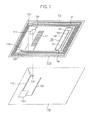
- Figs. 8A and 8B show an example of the configuration of a contactless IC card according to the related art.
- Fig. 8A shows a state in which the circuit for contactless communication is placed on a resin base.
- a contactless IC card as the actual product has a film or the like as an outer covering material placed on its surface so that the internal circuit is hidden.
- the configuration shown in Fig. 8A will be described.
- an antenna coil section 20 is placed at a location near the outer perimeter of the base 10.
- the antenna coil section 20 is formed by winding a conductor pattern of a predetermined width made of a conductor such as copper or aluminum a plurality of times (about four times in this example), and placing the windings at a predetermined interval, on the front surface near the outer perimeter of the base 10.
- One end 21 and the other end 22 of the antenna coil section 20 are connected to an IC chip 11, which is an integrated circuit component that performs communication processing.
- the one end 21 of the antenna coil section 20 is brought into electrical continuity with the back side of the base 10, and is connected to the IC chip 11 that performs communication processing, via a conductor pattern 14 on the back side.
- the other end 22 of the antenna coil section 20 is connected to the IC chip 11 via a conductor pattern 13.
- the one end 21 and the other end 22 of the antenna coil section 20 are connected to a capacitor 12 and an adjusting capacitor 30.
- the capacitor 12 and the adjusting capacitor 30 are also connected by using the conductor pattern 14 on the back side.
- the capacitor 12 is used to store electric charge generated by a carrier wave received by the antenna coil section 20, and obtain electric power for driving the IC chip 11.
- the capacitor 12 includes a first electrode section formed by a conductive pattern on the front side, and a second electrode section formed by a conductive pattern on the back side.
- the capacitor 12 stores electric charge on the first electrode section and the second electrode section that are opposed to each other via the base 10.
- Each of the electrode sections forming the capacitor 12 has a relatively large area so as to enable storage of relatively large electric charge.
- the adjusting capacitor 30 is used for the purpose of changing resonant frequency.
- the adjusting capacitor 30 includes a first conductor pattern 31 on the front side which is connected to the other end 22 of the antenna coil section 20, and a second conductor pattern 32 on the back side which is connected to the conductor pattern 14.
- the first conductor pattern 31 on the front side is placed in comb-tooth form, and the second conductor pattern 32 on the back side is placed so as to orthogonally intersect the comb-toothed portion. Electric charge is stored at their orthogonal intersections.
- the adjusting capacitor 30 is a small capacitance capacitor in comparison to the capacitor 12.
- the adjusting capacitor 30 is provided for the purpose of cutting off the comb-toothed conductor pattern partway to reduce the capacitor's capacitance when adjusting resonant frequency during the manufacturing process of the contactless IC card, thereby raising resonant frequency.
- Fig. 8B shows an equivalent circuit of the configuration of the contactless IC card shown in Fig. 8A .
- the IC chip 11, the capacitor 12, and the adjusting capacitor 30 are connected in parallel to the antenna coil section 20.
- An adjustment process to raise resonant frequency with the adjusting capacitor 30 is performed by cutting off the first conductor pattern 31 and the second conductor pattern 32 partway. This process is performed by, for example, boring a hole all the way through the base 10 at the cutting location of the first conductor pattern 31, and drawing out the first conductor pattern 31 or the second conductor pattern 32.
- This adjustment process of resonant frequency during the manufacturing process is performed automatically using an adjusting apparatus (not shown).
- the adjusting apparatus is configured to previously hold data on the cutting position for correcting the resonant frequency of the communication medium, determine the cutting position on the basis of the actually measured resonant frequency, and adjust the resonant frequency by boring a hole in the base at the determined position. Through this adjustment, a contactless IC card with an appropriate resonant frequency can be provided.
- Figs. 9A and 9B show an example of configuration with a center tap, different from the example shown in Figs. 8A and 8B .
- the antenna coil section 20 formed by winding a conductor pattern a plurality of times is placed at a location near the outer perimeter of the base 10.
- the one end 21 and the other end 22 of the antenna coil section 20 are connected to the IC chip 11, which is an integrated circuit component that performs communication processing.
- the one end 21 of the antenna coil section 20 is connected to the IC chip 11 that performs communication processing, via the conductor pattern 14 on the back side.
- the capacitor 12 is connected to the one end 21 of the antenna coil section 20.
- the capacitor 12 is connected to an end 24 of an antenna extension 23 that is extended from the other end 22 of the antenna coil section 20.
- the conductor pattern 14 on the back side is connected to the second conductor pattern 32, and the end 24 on the front side is connected to the first conductor pattern 31.
- Fig. 9B shows an equivalent circuit of the configuration of the contactless IC card shown in Fig. 9A .
- the IC chip 11 is connected to the antenna coil section 20, and the capacitor 12 and the adjusting capacitor 30 are connected via the antenna coil section 20 and the antenna extension 23.
- the other end 22 that is the connecting point of the antenna coil section 20 and the antenna extension 23 serves as a center tap.
- the adjustment process with the adjusting capacitor 30 is the same as that in the example shown in Figs. 8A and 8B .
- Japanese Unexamined Patent Application Publication No. 2003-67693 describes about a configuration for performing communication using a contactless IC card.
- the unnecessary portion of the adjusting capacitor 30 is detached from the circuit to reduce the capacitor's capacitance, thereby increasing resonant frequency.
- the reduction in the capacitor's capacitance can be done by boring a hole in the base 10 at the location where the adjusting capacitor 30 is placed, and thus can be performed relatively easily through an automatic adjustment process.
- a contactless IC card is sometimes used in situations where a magnetic sheet made of a magnetic material is brought into close proximity to the contactless IC card in order to improve antenna characteristics.
- placing a component such as a magnetic sheet in this way can improve radio communication characteristics, there is a possibility that the resonant frequency of the contactless IC card as a whole may change due to the influence of the component that has been placed.
- a contactless communication medium including a base made of an insulating material, an antenna coil section including a conductor wound in a planar shape on the base, a capacitor connected to the antenna coil section, a communication processing section that is connected to the antenna coil section and the capacitor to perform contactless communication processing, and an inductance adjusting conductor pattern that is connected in parallel to a part of the conductor in the antenna coil section and is placed on the base.
- the inductance adjusting conductor pattern by performing an adjusting operation of cutting off this inductance adjusting conductor pattern partway, the area of the antenna opening changes, thereby enabling an adjustment to increase inductance value. As this adjustment to increase inductance value is made, an adjustment to lower the resonant frequency of the antenna becomes possible.
- a conductor pattern is placed on a base made of a resin sheet to form an antenna pattern-placed medium, and then components such as an IC chip are further mounted, thereby forming a contactless communication medium 110.
- another sheet or the like is placed on the front and back of the base of the contactless communication medium 110, thereby completing a contactless IC card.
- Fig. 1A is a plan view of the front side of the contactless communication medium 110.
- Fig. 2 shows a front surface 110a and a back surface 110b of the contactless communication medium 110.
- the back surface 110b shown in Fig. 2 is a back surface as viewed from the front side. When the back surface is actually viewed, the back surface is upside down from what is shown in Fig. 2 .
- the contactless communication medium 110 is formed by a rectangular base similar to various kinds of cards or the like.
- an antenna coil section 120 is placed at a location near the outer perimeter of the contactless communication medium 110.
- the antenna coil section 120 is formed by placing and winding a conductor pattern of a predetermined width made of a conductor such as copper or aluminum a plurality of times (about four times in this example), on the front surface near the outer perimeter of the contactless communication medium 110.
- One end 121 and the other end 122 of the antenna coil section 120 are connected to an IC chip 111, which is an integrated circuit component that performs communication processing.
- the one end 121 of the antenna coil section 120 is brought into electrical continuity with the back side of the base, and is connected to the IC chip 111 that performs communication processing, via a conductor pattern 113 on the back side.
- the conductor pattern 113 on the back side is connected to the IC chip 111 by being brought into electrical continuity with the front side from the back side of the base at an IC chip connecting part 114.
- the other end 122 of the antenna coil section 120 is directly connected to the IC chip 111.
- the one end 121 and the other end 122 of the antenna coil section 120 are connected to a capacitor 112 and an adjusting capacitor 130.
- the capacitor 112 is connected to the one end 121 of the antenna coil section 120 via the conductor pattern 113.
- the capacitor 112 is connected to an end 124 of an antenna extension 123 that is extended from the other end 122 of the antenna coil section 120.
- the capacitor 112 is used to store electric charge generated by a carrier wave received by the antenna coil section 120, and obtain electric power for driving the IC chip 111.
- the capacitor 112 includes a first electrode section 112a formed by a conductive pattern on the front side, and a second electrode section 112b formed by a conductive pattern on the back side.
- the capacitor 112 stores electric charge on the first electrode section 112a and the second electrode section 112b that are opposed to each other via the base.
- Each of the electrode sections 112a and 112b forming the capacitor 112 has a relatively large area so as to enable storage of relatively large electric charge.
- the adjusting capacitor 130 is used for the purpose of changing resonant frequency. As shown in Fig. 2 , the adjusting capacitor 130 includes a first conductor pattern 131 on the front side which is connected to the other end 122 of the antenna coil section 120, and a second conductor pattern 132 on the back side which is connected to the second electrode section 112b.
- the first conductor pattern 131 on the front side is made up of a plurality of conductor patterns placed in a comb-tooth arrangement, and the second conductor pattern 132 on the back side is placed so as to orthogonally intersect the comb-toothed portion. Electric charge is stored at their orthogonal intersections.
- the adjusting capacitor 130 is a small capacitance capacitor in comparison to the capacitor 112.
- the adjusting capacitor 30 is provided for the purpose of cutting off the comb-toothed conductor pattern partway to reduce the capacitor's capacitance when adjusting resonant frequency during the manufacturing process of the contactless IC card, thereby raising resonant frequency.
- an inductance adjusting circuit 140 is connected partway along the antenna extension 123 of the antenna coil section 120.
- the extension 123 of the antenna coil section 120 is the antenna pattern located at the innermost perimeter of the antenna coil section 120.
- a conductor pattern forming the inductance adjusting circuit 140 is connected in parallel to a portion partway along the antenna extension 123 located at the innermost perimeter.
- in the inductance adjusting circuit 140 three conductor patterns 141, 142, and 143 are connected in parallel.
- each of a first conductor pattern 141 and a third conductor pattern 143 is connected, at a common connecting point 147, to the conductor pattern forming the antenna extension 123 of the antenna coil section 120.
- One end of the second conductor pattern 142 is connected to a connecting point 148 located near the one end of the first conductor pattern 141.
- each of the first conductor pattern 141 and the third conductor pattern 143 is connected, at a common connecting point 149, to the conductor pattern forming the antenna extension 123 of the antenna coil section 120.
- the other end of the third conductor pattern 143 is directly connected to the conductor pattern forming the antenna extension 123 of the antenna coil section 120.
- the substantially midway position of the first conductor pattern 141 serves as a trimming position 144
- the vicinity of the connecting point 149 serves as a trimming position 145
- the vicinity of the connecting point 147 serves as a trimming position 146.
- Each of the trimming positions 144, 145, and 146 is a position at which the conductor pattern is trimmed when adjusting inductance, and will be described later in detail.
- Fig. 1B shows an equivalent circuit of the circuit of the contactless communication medium 110 shown in Fig. 1A and Fig. 2 .
- the IC chip 111 is connected to the antenna coil section 120, and the capacitor 112 and the adjusting capacitor 130 are connected via the antenna coil section 120 and the antenna extension 123.
- the other end 122 that is the connecting point of the antenna coil section 120 and the antenna extension 123 serves as a center tap.
- the inductance adjusting circuit 140 is connected selectively in parallel to the antenna extension 123 of the antenna coil section.
- the capacitor's capacitance value can be adjusted using the adjusting capacitor 130, and the inductance value of the antenna coil section 120 can be also adjusted using the inductance adjusting circuit 140. Details of these adjustment processes will be described later.
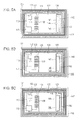
- Fig. 3 is an exploded view of the entire contactless IC card.
- the contactless IC card has an outer covering material 160 placed on the front surface of the contactless communication medium 110. While the outer covering material 160 is made of a relatively thick resin material, the outer covering material 160 may be made of a thin resin sheet.
- a magnetic sheet 180 and an adhesive sheet 170 are placed in order on the back surface of contactless communication medium 110. These components are integrated together, and assembled into a contactless IC card.
- the magnetic sheet 180 has such a size that is the same as at least the base forming the contactless communication medium 110 and allows the magnetic sheet 180 to cover the entire antenna coil section 120.
- the magnetic sheet 180 is provided with through holes 181, 182, and 183 at positions corresponding to the respective trimming positions 144, 145, and 146 of the contactless communication medium 110.
- the contactless IC card can be easily mounted to another electronic device for assembly into a communication apparatus. That is, as shown in Fig. 4 , for example, the contactless IC card according to this embodiment can be affixed to the back of a terminal apparatus 200 such as a mobile phone terminal, a smart phone, an information terminal, or an AV player, thereby assembling a communication apparatus with contactless communication capability.
- a terminal apparatus 200 such as a mobile phone terminal, a smart phone, an information terminal, or an AV player
- the provision of the magnetic sheet 180 allows such contactless communication to be performed in a favorable manner without being obstructed by the circuitry inside the terminal apparatus 200.
- the contactless communication medium 110 includes the adjusting capacitor 130 and the inductance adjusting circuit 140, as components for adjusting resonant frequency.
- the adjusting capacitor 130 is provided for the purpose of disconnecting a part or the entirety of the capacitor portion of the adjusting capacitor 130 to reduce capacitance value, thereby raising resonant frequency to achieve a specified resonant frequency.
- the resonant frequency of the antenna is adjusted by using the adjusting capacitor 130. This adjustment is made in the state when the contactless communication medium 110 exists alone, without the magnetic sheet 180 or the like shown in Fig. 3 being attached.
- the adjustment using the adjusting capacitor 130 is a process of raising resonant frequency.
- the magnetic sheet 180 is affixed to the back surface of the contactless communication medium 110, and the resonant frequency of the antenna of the contactless communication medium 110 is measured again.
- the resonant frequency may either become higher or lower in comparison to a specified resonant frequency due to the influence of the magnetic sheet 180.
- the higher frequency is corrected. This process is performed by boring a through hole at either one of the three trimming positions 144, 145, and 146 within the inductance adjusting circuit 140 to change the state of connection of the conductor patterns 141, 142, and 143.
- Figs. 5A to 5C show an example in which the state of connection of the conductor patterns 141, 142, and 143 is changed by boring a through hole at each of the three trimming positions 144, 145, and 146.
- Fig. 5A shows an example in which the first conductor pattern 141 is disconnected by forming a through hole at the trimming position 144 located partway along the first conductor pattern 141.
- the second conductor pattern 142 and the third conductor pattern 143 are connected in parallel to the antenna extension 123 of the antenna coil section 120, and the resonant frequency becomes lower as the first conductor pattern 141 is disconnected.
- Fig. 5B shows an example in which the first conductor pattern 141 and the second conductor pattern 142 are disconnected by forming a through hole at the trimming position 145 that is located at the connecting point 149 of the first conductor pattern 141 and the second conductor pattern 142.
- the third conductor pattern 143 is connected in parallel to the antenna extension 123 of the antenna coil section 120, and the resonant frequency becomes lower as the first conductor pattern 141 and the second conductor pattern 142 are disconnected.
- Fig. 5C shows an example in which all of the conductor patterns 141, 142, and 143 are disconnected by forming a through hole at the trimming position 146 that is located at the connecting point 147 of the conductor patterns 141, 142, and 143.
- the resonant frequency becomes lower as all of the conductor patterns 141, 142, and 143 are disconnected.
- a resonant frequency adjustment using a capacitor has a disadvantage in that since the capacitance (plate area) of the capacitor varies due to the influence of variations in line spacing of the antenna pattern, variations also tend to occur in the amount of adjustment of resonant frequency ( ⁇ f0).
- the inductance adjustment using the inductance adjusting circuit 140 according to this embodiment has an advantage in that even if variations occur in pattern line spacing, the number of coil windings in the antenna coil section does not change, so there is relatively little variation in the amount of resonant frequency adjustment ( ⁇ f0).
- the conductor patterns 141, 142, and 143 are connected in the manner as shown in Fig. 2 in this embodiment, in the case of making an adjustment in three stages, the adjustment can be made in any stage solely by boring a hole at one of the corresponding locations, thereby allowing the adjustment to be made in a favorable manner with few operations.
- FIG. 6 An example of circuit configuration different from that of the inductance adjusting circuit 140 shown in Figs. 1A and 1B and Fig. 2 is shown in Fig. 6 .
- a first conductor pattern 151, a second conductor pattern 152, and a third conductor pattern 153 are individually connected to the antenna extension 123 of the antenna coil section 120. Trimming positions 154, 155, and 156 are provided partway along the conductor patterns 151, 152, and 153, respectively.
- the contactless communication medium 110' shown in Fig. 6 is otherwise configured in the same manner as the contactless communication medium 110 shown in Figs. 1A and 1B and Fig. 2 .
- the inductance adjusting circuit 150 in the example shown in Fig. 6 is also configured as an inductance adjusting circuit including three conductor patterns, thus enabling inductance to be adjusted in at least three stages in the same manner as in the example shown in Figs. 1A and 1B .
- the trimming positions 154, 155, and 156 are individually provided for the respective conductor patterns.
- the trimming positions 154, 155, and 156 are individually provided for the respective conductor patterns.
- a second adjusting capacitor 190 is provided in addition to the adjusting capacitor 130, thereby allowing capacitance value to be varied independently with each of the adjusting capacitors 130 and 190.
- the contactless communication medium 110" is otherwise configured in the same manner as the contactless communication medium 110 shown in Figs. 1A and 1B and Fig. 2 .
- Providing the plurality of adjusting capacitors in this way can also increase the degree of freedom of adjustment.
- the adjustment using the adjusting capacitor 130 can be made prior to affixing a magnetic sheet, and after the magnetic sheet is affixed, adjustment can be performed by using the second adjusting capacitor 190 and the inductance adjusting circuit 140.
- the inductance adjusting circuit 140 or the like is provided in the case of a configuration with a so-called center tap (configuration shown in Figs. 9A and 9B ).
- this center tap scheme makes it possible to adjust only the coil (inductance value) on the outside of the coil connected to the IC, thereby reducing the influence of the communication distance or the like on communication characteristics.
- the inductance adjusting circuit 140 may be provided partway along the antenna coil section to enable adjustment of resonant frequency.
- the inductance adjusting circuit is provided with three conductor patterns, one or two, or three or more conductor patterns may be placed.
- the conductor patterns 141, 142, and 143 of the inductance adjusting circuit 140 shown in Fig. 1A or the like are positioned near the right end of the antenna coil section 120 as seen in Fig. 1A , for example, the substantially central portion of the antenna coil section 120 may be connected by the conductor patterns 141, 142, and 143.
- adjustment may be performed by using only the inductance adjusting circuit 140, and the adjusting capacitor 130 may be omitted.
- an adjustment to increase inductance value is made, thereby enabling an adjustment to lower the resonant frequency of the antenna. Therefore, when an adjustment to lower the resonant frequency of the antenna becomes necessary for the contactless communication medium, this can be easily handled by cutting off of the adjusting conductor pattern, or the like.
Landscapes
- Near-Field Transmission Systems (AREA)
- Support Of Aerials (AREA)
Applications Claiming Priority (1)
| Application Number | Priority Date | Filing Date | Title |
|---|---|---|---|
| JP2010108804A JP2011238016A (ja) | 2010-05-10 | 2010-05-10 | 非接触通信媒体、アンテナパターン配置媒体、通信装置及びアンテナ調整方法 |
Publications (3)
| Publication Number | Publication Date |
|---|---|
| EP2387109A2 true EP2387109A2 (fr) | 2011-11-16 |
| EP2387109A3 EP2387109A3 (fr) | 2012-12-26 |
| EP2387109B1 EP2387109B1 (fr) | 2017-07-26 |
Family
ID=44246993
Family Applications (1)
| Application Number | Title | Priority Date | Filing Date |
|---|---|---|---|
| EP11161835.1A Not-in-force EP2387109B1 (fr) | 2010-05-10 | 2011-04-11 | Support de communication sans contact, support d'antenne placé sur motif, appareil de communication et procédé de réglage d'antenne |
Country Status (7)
| Country | Link |
|---|---|
| US (1) | US8774712B2 (fr) |
| EP (1) | EP2387109B1 (fr) |
| JP (1) | JP2011238016A (fr) |
| CN (1) | CN102254212B (fr) |
| BR (1) | BRPI1102413A2 (fr) |
| RU (1) | RU2011117478A (fr) |
| TW (1) | TWI444900B (fr) |
Cited By (2)
| Publication number | Priority date | Publication date | Assignee | Title |
|---|---|---|---|---|
| EP2600362A3 (fr) * | 2011-11-30 | 2013-07-31 | Panasonic Corporation | Antenne, appareil d'antenne et appareil de communication |
| IT202100021308A1 (it) * | 2021-08-05 | 2023-02-05 | Tertium Tech S R L | Dispositivo di potenziamento di tag rfid/nfc |
Families Citing this family (45)
| Publication number | Priority date | Publication date | Assignee | Title |
|---|---|---|---|---|
| US11476566B2 (en) | 2009-03-09 | 2022-10-18 | Nucurrent, Inc. | Multi-layer-multi-turn structure for high efficiency wireless communication |
| US9208942B2 (en) * | 2009-03-09 | 2015-12-08 | Nucurrent, Inc. | Multi-layer-multi-turn structure for high efficiency wireless communication |
| US9232893B2 (en) | 2009-03-09 | 2016-01-12 | Nucurrent, Inc. | Method of operation of a multi-layer-multi-turn structure for high efficiency wireless communication |
| US9439287B2 (en) | 2009-03-09 | 2016-09-06 | Nucurrent, Inc. | Multi-layer wire structure for high efficiency wireless communication |
| US9444213B2 (en) | 2009-03-09 | 2016-09-13 | Nucurrent, Inc. | Method for manufacture of multi-layer wire structure for high efficiency wireless communication |
| US9300046B2 (en) | 2009-03-09 | 2016-03-29 | Nucurrent, Inc. | Method for manufacture of multi-layer-multi-turn high efficiency inductors |
| US9306358B2 (en) | 2009-03-09 | 2016-04-05 | Nucurrent, Inc. | Method for manufacture of multi-layer wire structure for high efficiency wireless communication |
| JP2011238016A (ja) * | 2010-05-10 | 2011-11-24 | Sony Corp | 非接触通信媒体、アンテナパターン配置媒体、通信装置及びアンテナ調整方法 |
| US8690412B2 (en) * | 2012-03-15 | 2014-04-08 | Apple Inc. | Backlight structures and backlight assemblies for electronic device displays |
| USD761736S1 (en) * | 2012-08-09 | 2016-07-19 | Sony Corporation | Non-contact type data carrier |
| JP6099352B2 (ja) * | 2012-10-17 | 2017-03-22 | デクセリアルズ株式会社 | 電子機器及びコイルモジュール |
| USD737255S1 (en) * | 2013-01-28 | 2015-08-25 | Sony Corporation | Non-contact type data reader |
| JP2014036437A (ja) * | 2013-04-18 | 2014-02-24 | Panasonic Corp | アンテナ、アンテナ装置および通信装置 |
| JP6079435B2 (ja) * | 2013-05-24 | 2017-02-15 | 大日本印刷株式会社 | 非接触ic媒体用アンテナシートと非接触ic媒体、非接触ic媒体の周波数調整方法 |
| TWI509523B (zh) * | 2013-06-11 | 2015-11-21 | China Steel Corp | 無線射頻標籤及其操作頻率之調整方法 |
| US20150054704A1 (en) * | 2013-08-23 | 2015-02-26 | Samsung Sdi Co., Ltd. | Antenna module for terminal device and method for manufacturing the same |
| TWI560937B (en) * | 2013-11-22 | 2016-12-01 | Wistron Neweb Corp | Near field communication antenna |
| USD747684S1 (en) * | 2014-05-16 | 2016-01-19 | Samsung Electronics Co., Ltd. | Battery cover for electronic device |
| USD812598S1 (en) * | 2015-06-17 | 2018-03-13 | Inside Secure | Data communication antenna |
| US10658847B2 (en) | 2015-08-07 | 2020-05-19 | Nucurrent, Inc. | Method of providing a single structure multi mode antenna for wireless power transmission using magnetic field coupling |
| US9941729B2 (en) | 2015-08-07 | 2018-04-10 | Nucurrent, Inc. | Single layer multi mode antenna for wireless power transmission using magnetic field coupling |
| US10063100B2 (en) | 2015-08-07 | 2018-08-28 | Nucurrent, Inc. | Electrical system incorporating a single structure multimode antenna for wireless power transmission using magnetic field coupling |
| US11205848B2 (en) | 2015-08-07 | 2021-12-21 | Nucurrent, Inc. | Method of providing a single structure multi mode antenna having a unitary body construction for wireless power transmission using magnetic field coupling |
| US9960628B2 (en) | 2015-08-07 | 2018-05-01 | Nucurrent, Inc. | Single structure multi mode antenna having a single layer structure with coils on opposing sides for wireless power transmission using magnetic field coupling |
| US9941743B2 (en) | 2015-08-07 | 2018-04-10 | Nucurrent, Inc. | Single structure multi mode antenna having a unitary body construction for wireless power transmission using magnetic field coupling |
| US9941590B2 (en) | 2015-08-07 | 2018-04-10 | Nucurrent, Inc. | Single structure multi mode antenna for wireless power transmission using magnetic field coupling having magnetic shielding |
| US10636563B2 (en) | 2015-08-07 | 2020-04-28 | Nucurrent, Inc. | Method of fabricating a single structure multi mode antenna for wireless power transmission using magnetic field coupling |
| US9948129B2 (en) | 2015-08-07 | 2018-04-17 | Nucurrent, Inc. | Single structure multi mode antenna for wireless power transmission using magnetic field coupling having an internal switch circuit |
| US9960629B2 (en) | 2015-08-07 | 2018-05-01 | Nucurrent, Inc. | Method of operating a single structure multi mode antenna for wireless power transmission using magnetic field coupling |
| US10985465B2 (en) | 2015-08-19 | 2021-04-20 | Nucurrent, Inc. | Multi-mode wireless antenna configurations |
| EP3166181A1 (fr) * | 2015-11-05 | 2017-05-10 | Gemalto Sa | Procede de fabrication d'antenne radiofrequence sur un support et antenne ainsi obtenue |
| CN109804516B (zh) | 2016-08-26 | 2021-11-02 | 纽卡润特有限公司 | 无线连接器系统 |
| US10892646B2 (en) | 2016-12-09 | 2021-01-12 | Nucurrent, Inc. | Method of fabricating an antenna having a substrate configured to facilitate through-metal energy transfer via near field magnetic coupling |
| US11264837B2 (en) | 2017-02-13 | 2022-03-01 | Nucurrent, Inc. | Transmitting base with antenna having magnetic shielding panes |
| US11277029B2 (en) | 2017-05-26 | 2022-03-15 | Nucurrent, Inc. | Multi coil array for wireless energy transfer with flexible device orientation |
| DE102018117364A1 (de) * | 2018-07-18 | 2020-01-23 | Infineon Technologies Ag | Verfahren und Vorrichtung zum Trimmen einer auf einem Träger aufgebrachten Antenne, Verfahren zum Herstellen einer Trägerstruktur, Trägerstruktur und Chipkarte |
| US11227712B2 (en) | 2019-07-19 | 2022-01-18 | Nucurrent, Inc. | Preemptive thermal mitigation for wireless power systems |
| US11271430B2 (en) | 2019-07-19 | 2022-03-08 | Nucurrent, Inc. | Wireless power transfer system with extended wireless charging range |
| US11056922B1 (en) | 2020-01-03 | 2021-07-06 | Nucurrent, Inc. | Wireless power transfer system for simultaneous transfer to multiple devices |
| CN111211406B (zh) * | 2020-03-24 | 2020-12-25 | 上海大学 | 一种单极子高铁天线 |
| US11283303B2 (en) | 2020-07-24 | 2022-03-22 | Nucurrent, Inc. | Area-apportioned wireless power antenna for maximized charging volume |
| US11881716B2 (en) | 2020-12-22 | 2024-01-23 | Nucurrent, Inc. | Ruggedized communication for wireless power systems in multi-device environments |
| US11876386B2 (en) | 2020-12-22 | 2024-01-16 | Nucurrent, Inc. | Detection of foreign objects in large charging volume applications |
| US11695302B2 (en) | 2021-02-01 | 2023-07-04 | Nucurrent, Inc. | Segmented shielding for wide area wireless power transmitter |
| US11831174B2 (en) | 2022-03-01 | 2023-11-28 | Nucurrent, Inc. | Cross talk and interference mitigation in dual wireless power transmitter |
Citations (2)
| Publication number | Priority date | Publication date | Assignee | Title |
|---|---|---|---|---|
| JP2003067693A (ja) | 2001-08-27 | 2003-03-07 | Fujitsu Ltd | 非接触icカード |
| JP2010108804A (ja) | 2008-10-31 | 2010-05-13 | Panasonic Corp | 天井扇風機 |
Family Cites Families (47)
| Publication number | Priority date | Publication date | Assignee | Title |
|---|---|---|---|---|
| JPH04321190A (ja) * | 1991-04-22 | 1992-11-11 | Mitsubishi Electric Corp | 非接触型携帯記憶装置のアンテナ回路 |
| JP3307307B2 (ja) * | 1997-12-19 | 2002-07-24 | 株式会社村田製作所 | 多層型高周波電子部品 |
| US6412702B1 (en) * | 1999-01-25 | 2002-07-02 | Mitsumi Electric Co., Ltd. | Non-contact IC card having an antenna coil formed by a plating method |
| JP4286977B2 (ja) * | 1999-07-02 | 2009-07-01 | 大日本印刷株式会社 | 非接触型icカードとそのアンテナ特性調整方法 |
| FR2808648B1 (fr) * | 2000-05-03 | 2004-07-30 | Schlumberger Systems & Service | Antenne pour carte a circuit integre et procede d'ajustement de l'inductance d'une telle antenne |
| TW502492B (en) * | 2000-05-30 | 2002-09-11 | Alps Electric Co Ltd | Electronic circuit unit |
| JP4628611B2 (ja) * | 2000-10-27 | 2011-02-09 | 三菱マテリアル株式会社 | アンテナ |
| FI113809B (fi) * | 2000-11-01 | 2004-06-15 | Rafsec Oy | Menetelmä älytarran valmistamiseksi sekä älytarra |
| JP3781109B2 (ja) * | 2002-01-31 | 2006-05-31 | 三菱マテリアル株式会社 | Rfid用トランスポンダのアンテナコイルの構造及び該アンテナコイルを用いた共振周波数の調整方法 |
| JP4006585B2 (ja) * | 2002-08-21 | 2007-11-14 | 三菱マテリアル株式会社 | Rfid用トランスポンダのアンテナコイル構造及び共振周波数の調整方法 |
| JP4016261B2 (ja) * | 2002-09-24 | 2007-12-05 | 三菱マテリアル株式会社 | Rfid用トランスポンダ及び共振周波数の調整方法 |
| JP3975918B2 (ja) * | 2002-09-27 | 2007-09-12 | ソニー株式会社 | アンテナ装置 |
| WO2004030148A1 (fr) * | 2002-09-30 | 2004-04-08 | The Furukawa Electric Co., Ltd. | Etiquette rfid et son procede de production |
| EP1563570A1 (fr) * | 2002-11-07 | 2005-08-17 | Fractus, S.A. | Boitier de circuit integre incluant une antenne miniature |
| US7930815B2 (en) * | 2003-04-11 | 2011-04-26 | Avery Dennison Corporation | Conductive pattern and method of making |
| US20040200061A1 (en) * | 2003-04-11 | 2004-10-14 | Coleman James P. | Conductive pattern and method of making |
| JP2005165703A (ja) * | 2003-12-03 | 2005-06-23 | Hitachi Ltd | 非接触識別媒体 |
| JP4494855B2 (ja) * | 2004-04-27 | 2010-06-30 | 古河電気工業株式会社 | Rfidタグ及びrfidタグの共振周波数の調整方法 |
| JP2006053653A (ja) * | 2004-08-10 | 2006-02-23 | Olympus Corp | 情報記憶媒体 |
| JP4663346B2 (ja) * | 2005-02-01 | 2011-04-06 | 富士通株式会社 | メアンダラインアンテナ |
| JP2007214754A (ja) * | 2006-02-08 | 2007-08-23 | Matsushita Electric Ind Co Ltd | アンテナ装置 |
| JP4755921B2 (ja) * | 2006-02-24 | 2011-08-24 | 富士通株式会社 | Rfidタグ |
| CN101331651B (zh) * | 2006-04-14 | 2013-01-30 | 株式会社村田制作所 | 天线 |
| JP4618461B2 (ja) * | 2006-05-08 | 2011-01-26 | 日立金属株式会社 | 高周波回路、高周波部品及び通信装置 |
| JP3957000B1 (ja) * | 2006-07-07 | 2007-08-08 | 株式会社村田製作所 | 基板実装用アンテナコイル及びアンテナ装置 |
| JP4811935B2 (ja) * | 2006-07-27 | 2011-11-09 | 株式会社村田製作所 | ノイズフィルタアレイ |
| CN101485046A (zh) * | 2006-08-08 | 2009-07-15 | 松下电器产业株式会社 | 射频识别磁片、非接触式ic卡及便携式移动通信设备 |
| DE102007027838B4 (de) * | 2007-06-13 | 2021-01-14 | Leonhard Kurz Gmbh & Co. Kg | Mehrschichtiges Folienelement |
| JP5151404B2 (ja) * | 2007-11-07 | 2013-02-27 | 凸版印刷株式会社 | 複合型icカードおよびその製造方法 |
| JP5118462B2 (ja) * | 2007-12-12 | 2013-01-16 | 日本発條株式会社 | コイルアンテナおよび非接触情報媒体 |
| EP2717196B1 (fr) * | 2007-12-26 | 2020-05-13 | Murata Manufacturing Co., Ltd. | Appareil d'antenne et dispositif a puce sans fil |
| JP5029371B2 (ja) * | 2008-01-08 | 2012-09-19 | パナソニック株式会社 | アンテナ装置およびその調整方法 |
| JP2009200748A (ja) * | 2008-02-20 | 2009-09-03 | Fujikura Ltd | コイルアンテナ装置、非接触式電子カード及び携帯通信機器 |
| JP2009271656A (ja) * | 2008-05-02 | 2009-11-19 | Dainippon Printing Co Ltd | Icカード及びその製造方法 |
| WO2009142068A1 (fr) * | 2008-05-22 | 2009-11-26 | 株式会社村田製作所 | Dispositif à circuit intégré sans fil et son procédé de fabrication |
| JP5516407B2 (ja) * | 2008-09-11 | 2014-06-11 | 日本電気株式会社 | 構造体、アンテナ、通信装置、及び電子部品 |
| WO2010089914A1 (fr) * | 2009-02-05 | 2010-08-12 | 株式会社村田製作所 | Antenne magnétique |
| US8076996B2 (en) * | 2009-02-10 | 2011-12-13 | Electronics And Telecommunications Research Institute | Hybrid balun apparatus |
| JP4788791B2 (ja) * | 2009-02-27 | 2011-10-05 | Tdk株式会社 | アンテナ装置 |
| US8773311B2 (en) * | 2009-03-06 | 2014-07-08 | Nec Corporation | Resonator antenna and communication apparatus |
| WO2010104179A1 (fr) * | 2009-03-13 | 2010-09-16 | 株式会社村田製作所 | Circuit de traitement de signal et appareil d'antenne |
| WO2010120218A1 (fr) * | 2009-04-15 | 2010-10-21 | Laird Technologies Ab | Dispositif d'antenne multibande et dispositif de communication radio portable comprenant un tel dispositif d'antenne |
| US8201748B2 (en) * | 2009-04-27 | 2012-06-19 | Impinj, Inc. | Packaged RFID IC with integrated antenna |
| KR101215303B1 (ko) * | 2009-07-21 | 2012-12-26 | 한국전자통신연구원 | 엘티씨씨 인덕터를 포함하는 전자 장치 |
| CN104617374B (zh) * | 2009-11-20 | 2018-04-06 | 株式会社村田制作所 | 移动通信终端 |
| JP2011238016A (ja) * | 2010-05-10 | 2011-11-24 | Sony Corp | 非接触通信媒体、アンテナパターン配置媒体、通信装置及びアンテナ調整方法 |
| JP5234084B2 (ja) * | 2010-11-05 | 2013-07-10 | 株式会社村田製作所 | アンテナ装置および通信端末装置 |
-
2010
- 2010-05-10 JP JP2010108804A patent/JP2011238016A/ja active Pending
-
2011
- 2011-04-11 EP EP11161835.1A patent/EP2387109B1/fr not_active Not-in-force
- 2011-04-26 US US13/066,842 patent/US8774712B2/en not_active Expired - Fee Related
- 2011-04-29 TW TW100115125A patent/TWI444900B/zh not_active IP Right Cessation
- 2011-04-29 RU RU2011117478/07A patent/RU2011117478A/ru unknown
- 2011-05-03 CN CN201110112728.XA patent/CN102254212B/zh not_active Expired - Fee Related
- 2011-05-04 BR BRPI1102413-5A patent/BRPI1102413A2/pt not_active IP Right Cessation
Patent Citations (2)
| Publication number | Priority date | Publication date | Assignee | Title |
|---|---|---|---|---|
| JP2003067693A (ja) | 2001-08-27 | 2003-03-07 | Fujitsu Ltd | 非接触icカード |
| JP2010108804A (ja) | 2008-10-31 | 2010-05-13 | Panasonic Corp | 天井扇風機 |
Cited By (4)
| Publication number | Priority date | Publication date | Assignee | Title |
|---|---|---|---|---|
| EP2600362A3 (fr) * | 2011-11-30 | 2013-07-31 | Panasonic Corporation | Antenne, appareil d'antenne et appareil de communication |
| US8669909B2 (en) | 2011-11-30 | 2014-03-11 | Panasonic Corporation | Antenna, antenna apparatus, and communication apparatus |
| US9172141B2 (en) | 2011-11-30 | 2015-10-27 | Panasonic Corporation | Antenna, antenna apparatus, and communication apparatus |
| IT202100021308A1 (it) * | 2021-08-05 | 2023-02-05 | Tertium Tech S R L | Dispositivo di potenziamento di tag rfid/nfc |
Also Published As
| Publication number | Publication date |
|---|---|
| US8774712B2 (en) | 2014-07-08 |
| CN102254212A (zh) | 2011-11-23 |
| RU2011117478A (ru) | 2012-11-10 |
| US20110275318A1 (en) | 2011-11-10 |
| EP2387109B1 (fr) | 2017-07-26 |
| JP2011238016A (ja) | 2011-11-24 |
| TWI444900B (zh) | 2014-07-11 |
| TW201207741A (en) | 2012-02-16 |
| BRPI1102413A2 (pt) | 2012-10-16 |
| EP2387109A3 (fr) | 2012-12-26 |
| CN102254212B (zh) | 2017-03-01 |
Similar Documents
| Publication | Publication Date | Title |
|---|---|---|
| US8774712B2 (en) | Contactless communication medium, antenna pattern-placed medium, communication apparatus, and antenna adjusting method | |
| US11070075B2 (en) | Electronic device including non-contact charging module and battery | |
| CN101836330B (zh) | 天线电路及其电阻降低方法、以及应答器 | |
| US9172141B2 (en) | Antenna, antenna apparatus, and communication apparatus | |
| EP1772927B1 (fr) | Antenne et étiquette sans contact | |
| US9104954B2 (en) | Radiofrequency transponder device with optimized passive resonant circuit | |
| CN201402855Y (zh) | 天线装置 | |
| JP6090536B2 (ja) | アンテナ装置、アンテナモジュールおよび通信端末装置 | |
| CN103797642B (zh) | 天线装置及电子设备 | |
| JP2002207987A (ja) | カードまたはラベル用の非接触電子モジュール | |
| CN203277640U (zh) | 天线、天线装置及通信装置 | |
| US9208427B2 (en) | Contactless communication medium, antenna pattern arrangement medium, communication apparatus, and communication method | |
| EP4050516A2 (fr) | Corps de carte pour une carte intelligente, carte intelligente et procédé d'intégration d'un fil | |
| KR20080096930A (ko) | 알에프아이디 안테나의 제조방법 | |
| KR101283822B1 (ko) | 튜닝 인레이 | |
| WO2008115022A1 (fr) | Antenne d'identification par radiofréquence et son procédé de fabrication | |
| JP2014036437A (ja) | アンテナ、アンテナ装置および通信装置 | |
| JP2017156929A (ja) | アンテナシートの製造方法、アンテナシート及び非接触情報媒体 | |
| JP2016162136A (ja) | Ic記録媒体、アンテナシート及びインレット |
Legal Events
| Date | Code | Title | Description |
|---|---|---|---|
| 17P | Request for examination filed |
Effective date: 20110426 |
|
| AK | Designated contracting states |
Kind code of ref document: A2 Designated state(s): AL AT BE BG CH CY CZ DE DK EE ES FI FR GB GR HR HU IE IS IT LI LT LU LV MC MK MT NL NO PL PT RO RS SE SI SK SM TR |
|
| AX | Request for extension of the european patent |
Extension state: BA ME |
|
| PUAI | Public reference made under article 153(3) epc to a published international application that has entered the european phase |
Free format text: ORIGINAL CODE: 0009012 |
|
| PUAL | Search report despatched |
Free format text: ORIGINAL CODE: 0009013 |
|
| AK | Designated contracting states |
Kind code of ref document: A3 Designated state(s): AL AT BE BG CH CY CZ DE DK EE ES FI FR GB GR HR HU IE IS IT LI LT LU LV MC MK MT NL NO PL PT RO RS SE SI SK SM TR |
|
| AX | Request for extension of the european patent |
Extension state: BA ME |
|
| RIC1 | Information provided on ipc code assigned before grant |
Ipc: H01Q 7/00 20060101AFI20121120BHEP Ipc: G06K 19/077 20060101ALI20121120BHEP Ipc: H01Q 1/22 20060101ALI20121120BHEP Ipc: G06K 19/07 20060101ALI20121120BHEP |
|
| 17Q | First examination report despatched |
Effective date: 20131121 |
|
| GRAP | Despatch of communication of intention to grant a patent |
Free format text: ORIGINAL CODE: EPIDOSNIGR1 |
|
| STAA | Information on the status of an ep patent application or granted ep patent |
Free format text: STATUS: GRANT OF PATENT IS INTENDED |
|
| INTG | Intention to grant announced |
Effective date: 20170217 |
|
| RIC1 | Information provided on ipc code assigned before grant |
Ipc: H01Q 1/22 20060101ALI20170206BHEP Ipc: H01Q 7/00 20060101AFI20170206BHEP |
|
| GRAS | Grant fee paid |
Free format text: ORIGINAL CODE: EPIDOSNIGR3 |
|
| GRAA | (expected) grant |
Free format text: ORIGINAL CODE: 0009210 |
|
| STAA | Information on the status of an ep patent application or granted ep patent |
Free format text: STATUS: THE PATENT HAS BEEN GRANTED |
|
| AK | Designated contracting states |
Kind code of ref document: B1 Designated state(s): AL AT BE BG CH CY CZ DE DK EE ES FI FR GB GR HR HU IE IS IT LI LT LU LV MC MK MT NL NO PL PT RO RS SE SI SK SM TR |
|
| REG | Reference to a national code |
Ref country code: GB Ref legal event code: FG4D |
|
| REG | Reference to a national code |
Ref country code: CH Ref legal event code: EP |
|
| REG | Reference to a national code |
Ref country code: AT Ref legal event code: REF Ref document number: 913102 Country of ref document: AT Kind code of ref document: T Effective date: 20170815 |
|
| REG | Reference to a national code |
Ref country code: IE Ref legal event code: FG4D |
|
| REG | Reference to a national code |
Ref country code: DE Ref legal event code: R096 Ref document number: 602011039867 Country of ref document: DE |
|
| REG | Reference to a national code |
Ref country code: NL Ref legal event code: MP Effective date: 20170726 |
|
| REG | Reference to a national code |
Ref country code: LT Ref legal event code: MG4D |
|
| REG | Reference to a national code |
Ref country code: AT Ref legal event code: MK05 Ref document number: 913102 Country of ref document: AT Kind code of ref document: T Effective date: 20170726 |
|
| PG25 | Lapsed in a contracting state [announced via postgrant information from national office to epo] |
Ref country code: HR Free format text: LAPSE BECAUSE OF FAILURE TO SUBMIT A TRANSLATION OF THE DESCRIPTION OR TO PAY THE FEE WITHIN THE PRESCRIBED TIME-LIMIT Effective date: 20170726 Ref country code: SE Free format text: LAPSE BECAUSE OF FAILURE TO SUBMIT A TRANSLATION OF THE DESCRIPTION OR TO PAY THE FEE WITHIN THE PRESCRIBED TIME-LIMIT Effective date: 20170726 Ref country code: LT Free format text: LAPSE BECAUSE OF FAILURE TO SUBMIT A TRANSLATION OF THE DESCRIPTION OR TO PAY THE FEE WITHIN THE PRESCRIBED TIME-LIMIT Effective date: 20170726 Ref country code: NO Free format text: LAPSE BECAUSE OF FAILURE TO SUBMIT A TRANSLATION OF THE DESCRIPTION OR TO PAY THE FEE WITHIN THE PRESCRIBED TIME-LIMIT Effective date: 20171026 Ref country code: FI Free format text: LAPSE BECAUSE OF FAILURE TO SUBMIT A TRANSLATION OF THE DESCRIPTION OR TO PAY THE FEE WITHIN THE PRESCRIBED TIME-LIMIT Effective date: 20170726 Ref country code: NL Free format text: LAPSE BECAUSE OF FAILURE TO SUBMIT A TRANSLATION OF THE DESCRIPTION OR TO PAY THE FEE WITHIN THE PRESCRIBED TIME-LIMIT Effective date: 20170726 Ref country code: AT Free format text: LAPSE BECAUSE OF FAILURE TO SUBMIT A TRANSLATION OF THE DESCRIPTION OR TO PAY THE FEE WITHIN THE PRESCRIBED TIME-LIMIT Effective date: 20170726 |
|
| PG25 | Lapsed in a contracting state [announced via postgrant information from national office to epo] |
Ref country code: GR Free format text: LAPSE BECAUSE OF FAILURE TO SUBMIT A TRANSLATION OF THE DESCRIPTION OR TO PAY THE FEE WITHIN THE PRESCRIBED TIME-LIMIT Effective date: 20171027 Ref country code: BG Free format text: LAPSE BECAUSE OF FAILURE TO SUBMIT A TRANSLATION OF THE DESCRIPTION OR TO PAY THE FEE WITHIN THE PRESCRIBED TIME-LIMIT Effective date: 20171026 Ref country code: IS Free format text: LAPSE BECAUSE OF FAILURE TO SUBMIT A TRANSLATION OF THE DESCRIPTION OR TO PAY THE FEE WITHIN THE PRESCRIBED TIME-LIMIT Effective date: 20171126 Ref country code: RS Free format text: LAPSE BECAUSE OF FAILURE TO SUBMIT A TRANSLATION OF THE DESCRIPTION OR TO PAY THE FEE WITHIN THE PRESCRIBED TIME-LIMIT Effective date: 20170726 Ref country code: PL Free format text: LAPSE BECAUSE OF FAILURE TO SUBMIT A TRANSLATION OF THE DESCRIPTION OR TO PAY THE FEE WITHIN THE PRESCRIBED TIME-LIMIT Effective date: 20170726 Ref country code: ES Free format text: LAPSE BECAUSE OF FAILURE TO SUBMIT A TRANSLATION OF THE DESCRIPTION OR TO PAY THE FEE WITHIN THE PRESCRIBED TIME-LIMIT Effective date: 20170726 Ref country code: LV Free format text: LAPSE BECAUSE OF FAILURE TO SUBMIT A TRANSLATION OF THE DESCRIPTION OR TO PAY THE FEE WITHIN THE PRESCRIBED TIME-LIMIT Effective date: 20170726 |
|
| REG | Reference to a national code |
Ref country code: FR Ref legal event code: PLFP Year of fee payment: 8 |
|
| PG25 | Lapsed in a contracting state [announced via postgrant information from national office to epo] |
Ref country code: DK Free format text: LAPSE BECAUSE OF FAILURE TO SUBMIT A TRANSLATION OF THE DESCRIPTION OR TO PAY THE FEE WITHIN THE PRESCRIBED TIME-LIMIT Effective date: 20170726 Ref country code: RO Free format text: LAPSE BECAUSE OF FAILURE TO SUBMIT A TRANSLATION OF THE DESCRIPTION OR TO PAY THE FEE WITHIN THE PRESCRIBED TIME-LIMIT Effective date: 20170726 Ref country code: CZ Free format text: LAPSE BECAUSE OF FAILURE TO SUBMIT A TRANSLATION OF THE DESCRIPTION OR TO PAY THE FEE WITHIN THE PRESCRIBED TIME-LIMIT Effective date: 20170726 |
|
| REG | Reference to a national code |
Ref country code: DE Ref legal event code: R097 Ref document number: 602011039867 Country of ref document: DE |
|
| PG25 | Lapsed in a contracting state [announced via postgrant information from national office to epo] |
Ref country code: SM Free format text: LAPSE BECAUSE OF FAILURE TO SUBMIT A TRANSLATION OF THE DESCRIPTION OR TO PAY THE FEE WITHIN THE PRESCRIBED TIME-LIMIT Effective date: 20170726 Ref country code: IT Free format text: LAPSE BECAUSE OF FAILURE TO SUBMIT A TRANSLATION OF THE DESCRIPTION OR TO PAY THE FEE WITHIN THE PRESCRIBED TIME-LIMIT Effective date: 20170726 Ref country code: SK Free format text: LAPSE BECAUSE OF FAILURE TO SUBMIT A TRANSLATION OF THE DESCRIPTION OR TO PAY THE FEE WITHIN THE PRESCRIBED TIME-LIMIT Effective date: 20170726 Ref country code: EE Free format text: LAPSE BECAUSE OF FAILURE TO SUBMIT A TRANSLATION OF THE DESCRIPTION OR TO PAY THE FEE WITHIN THE PRESCRIBED TIME-LIMIT Effective date: 20170726 |
|
| PLBE | No opposition filed within time limit |
Free format text: ORIGINAL CODE: 0009261 |
|
| STAA | Information on the status of an ep patent application or granted ep patent |
Free format text: STATUS: NO OPPOSITION FILED WITHIN TIME LIMIT |
|
| 26N | No opposition filed |
Effective date: 20180430 |
|
| PG25 | Lapsed in a contracting state [announced via postgrant information from national office to epo] |
Ref country code: SI Free format text: LAPSE BECAUSE OF FAILURE TO SUBMIT A TRANSLATION OF THE DESCRIPTION OR TO PAY THE FEE WITHIN THE PRESCRIBED TIME-LIMIT Effective date: 20170726 |
|
| PG25 | Lapsed in a contracting state [announced via postgrant information from national office to epo] |
Ref country code: MC Free format text: LAPSE BECAUSE OF FAILURE TO SUBMIT A TRANSLATION OF THE DESCRIPTION OR TO PAY THE FEE WITHIN THE PRESCRIBED TIME-LIMIT Effective date: 20170726 |
|
| REG | Reference to a national code |
Ref country code: CH Ref legal event code: PL |
|
| REG | Reference to a national code |
Ref country code: BE Ref legal event code: MM Effective date: 20180430 |
|
| REG | Reference to a national code |
Ref country code: IE Ref legal event code: MM4A |
|
| PG25 | Lapsed in a contracting state [announced via postgrant information from national office to epo] |
Ref country code: LU Free format text: LAPSE BECAUSE OF NON-PAYMENT OF DUE FEES Effective date: 20180411 |
|
| PG25 | Lapsed in a contracting state [announced via postgrant information from national office to epo] |
Ref country code: CH Free format text: LAPSE BECAUSE OF NON-PAYMENT OF DUE FEES Effective date: 20180430 Ref country code: BE Free format text: LAPSE BECAUSE OF NON-PAYMENT OF DUE FEES Effective date: 20180430 Ref country code: LI Free format text: LAPSE BECAUSE OF NON-PAYMENT OF DUE FEES Effective date: 20180430 |
|
| PG25 | Lapsed in a contracting state [announced via postgrant information from national office to epo] |
Ref country code: IE Free format text: LAPSE BECAUSE OF NON-PAYMENT OF DUE FEES Effective date: 20180411 |
|
| PG25 | Lapsed in a contracting state [announced via postgrant information from national office to epo] |
Ref country code: MT Free format text: LAPSE BECAUSE OF NON-PAYMENT OF DUE FEES Effective date: 20180411 |
|
| PG25 | Lapsed in a contracting state [announced via postgrant information from national office to epo] |
Ref country code: TR Free format text: LAPSE BECAUSE OF FAILURE TO SUBMIT A TRANSLATION OF THE DESCRIPTION OR TO PAY THE FEE WITHIN THE PRESCRIBED TIME-LIMIT Effective date: 20170726 |
|
| PG25 | Lapsed in a contracting state [announced via postgrant information from national office to epo] |
Ref country code: HU Free format text: LAPSE BECAUSE OF FAILURE TO SUBMIT A TRANSLATION OF THE DESCRIPTION OR TO PAY THE FEE WITHIN THE PRESCRIBED TIME-LIMIT; INVALID AB INITIO Effective date: 20110411 Ref country code: PT Free format text: LAPSE BECAUSE OF FAILURE TO SUBMIT A TRANSLATION OF THE DESCRIPTION OR TO PAY THE FEE WITHIN THE PRESCRIBED TIME-LIMIT Effective date: 20170726 |
|
| PG25 | Lapsed in a contracting state [announced via postgrant information from national office to epo] |
Ref country code: CY Free format text: LAPSE BECAUSE OF FAILURE TO SUBMIT A TRANSLATION OF THE DESCRIPTION OR TO PAY THE FEE WITHIN THE PRESCRIBED TIME-LIMIT Effective date: 20170726 Ref country code: MK Free format text: LAPSE BECAUSE OF NON-PAYMENT OF DUE FEES Effective date: 20170726 |
|
| PG25 | Lapsed in a contracting state [announced via postgrant information from national office to epo] |
Ref country code: AL Free format text: LAPSE BECAUSE OF FAILURE TO SUBMIT A TRANSLATION OF THE DESCRIPTION OR TO PAY THE FEE WITHIN THE PRESCRIBED TIME-LIMIT Effective date: 20170726 |
|
| PGFP | Annual fee paid to national office [announced via postgrant information from national office to epo] |
Ref country code: FR Payment date: 20210323 Year of fee payment: 11 |
|
| PGFP | Annual fee paid to national office [announced via postgrant information from national office to epo] |
Ref country code: GB Payment date: 20210324 Year of fee payment: 11 |
|
| PGFP | Annual fee paid to national office [announced via postgrant information from national office to epo] |
Ref country code: DE Payment date: 20210323 Year of fee payment: 11 |
|
| REG | Reference to a national code |
Ref country code: DE Ref legal event code: R119 Ref document number: 602011039867 Country of ref document: DE |
|
| GBPC | Gb: european patent ceased through non-payment of renewal fee |
Effective date: 20220411 |
|
| PG25 | Lapsed in a contracting state [announced via postgrant information from national office to epo] |
Ref country code: GB Free format text: LAPSE BECAUSE OF NON-PAYMENT OF DUE FEES Effective date: 20220411 Ref country code: FR Free format text: LAPSE BECAUSE OF NON-PAYMENT OF DUE FEES Effective date: 20220430 Ref country code: DE Free format text: LAPSE BECAUSE OF NON-PAYMENT OF DUE FEES Effective date: 20221103 |