EP2386400A1 - Boîtier de dispositif électronique doté d'un cadre de motif d'antenne intégré, moule correspondant et son procédé de fabrication - Google Patents
Boîtier de dispositif électronique doté d'un cadre de motif d'antenne intégré, moule correspondant et son procédé de fabrication Download PDFInfo
- Publication number
- EP2386400A1 EP2386400A1 EP11250429A EP11250429A EP2386400A1 EP 2386400 A1 EP2386400 A1 EP 2386400A1 EP 11250429 A EP11250429 A EP 11250429A EP 11250429 A EP11250429 A EP 11250429A EP 2386400 A1 EP2386400 A1 EP 2386400A1
- Authority
- EP
- European Patent Office
- Prior art keywords
- case
- frame
- radiator
- mold
- antenna pattern
- Prior art date
- Legal status (The legal status is an assumption and is not a legal conclusion. Google has not performed a legal analysis and makes no representation as to the accuracy of the status listed.)
- Withdrawn
Links
Images


Classifications
-
- B—PERFORMING OPERATIONS; TRANSPORTING
- B29—WORKING OF PLASTICS; WORKING OF SUBSTANCES IN A PLASTIC STATE IN GENERAL
- B29C—SHAPING OR JOINING OF PLASTICS; SHAPING OF MATERIAL IN A PLASTIC STATE, NOT OTHERWISE PROVIDED FOR; AFTER-TREATMENT OF THE SHAPED PRODUCTS, e.g. REPAIRING
- B29C45/00—Injection moulding, i.e. forcing the required volume of moulding material through a nozzle into a closed mould; Apparatus therefor
- B29C45/14—Injection moulding, i.e. forcing the required volume of moulding material through a nozzle into a closed mould; Apparatus therefor incorporating preformed parts or layers, e.g. injection moulding around inserts or for coating articles
- B29C45/14065—Positioning or centering articles in the mould
-
- B—PERFORMING OPERATIONS; TRANSPORTING
- B29—WORKING OF PLASTICS; WORKING OF SUBSTANCES IN A PLASTIC STATE IN GENERAL
- B29C—SHAPING OR JOINING OF PLASTICS; SHAPING OF MATERIAL IN A PLASTIC STATE, NOT OTHERWISE PROVIDED FOR; AFTER-TREATMENT OF THE SHAPED PRODUCTS, e.g. REPAIRING
- B29C45/00—Injection moulding, i.e. forcing the required volume of moulding material through a nozzle into a closed mould; Apparatus therefor
- B29C45/16—Making multilayered or multicoloured articles
- B29C45/1671—Making multilayered or multicoloured articles with an insert
-
- H—ELECTRICITY
- H01—ELECTRIC ELEMENTS
- H01Q—ANTENNAS, i.e. RADIO AERIALS
- H01Q1/00—Details of, or arrangements associated with, antennas
- H01Q1/12—Supports; Mounting means
- H01Q1/22—Supports; Mounting means by structural association with other equipment or articles
- H01Q1/24—Supports; Mounting means by structural association with other equipment or articles with receiving set
- H01Q1/241—Supports; Mounting means by structural association with other equipment or articles with receiving set used in mobile communications, e.g. GSM
- H01Q1/242—Supports; Mounting means by structural association with other equipment or articles with receiving set used in mobile communications, e.g. GSM specially adapted for hand-held use
- H01Q1/243—Supports; Mounting means by structural association with other equipment or articles with receiving set used in mobile communications, e.g. GSM specially adapted for hand-held use with built-in antennas
-
- H—ELECTRICITY
- H01—ELECTRIC ELEMENTS
- H01Q—ANTENNAS, i.e. RADIO AERIALS
- H01Q1/00—Details of, or arrangements associated with, antennas
- H01Q1/40—Radiating elements coated with or embedded in protective material
-
- H—ELECTRICITY
- H01—ELECTRIC ELEMENTS
- H01Q—ANTENNAS, i.e. RADIO AERIALS
- H01Q5/00—Arrangements for simultaneous operation of antennas on two or more different wavebands, e.g. dual-band or multi-band arrangements
- H01Q5/40—Imbricated or interleaved structures; Combined or electromagnetically coupled arrangements, e.g. comprising two or more non-connected fed radiating elements
-
- H—ELECTRICITY
- H01—ELECTRIC ELEMENTS
- H01Q—ANTENNAS, i.e. RADIO AERIALS
- H01Q7/00—Loop antennas with a substantially uniform current distribution around the loop and having a directional radiation pattern in a plane perpendicular to the plane of the loop
-
- H—ELECTRICITY
- H01—ELECTRIC ELEMENTS
- H01Q—ANTENNAS, i.e. RADIO AERIALS
- H01Q9/00—Electrically-short antennas having dimensions not more than twice the operating wavelength and consisting of conductive active radiating elements
- H01Q9/04—Resonant antennas
- H01Q9/0407—Substantially flat resonant element parallel to ground plane, e.g. patch antenna
- H01Q9/0421—Substantially flat resonant element parallel to ground plane, e.g. patch antenna with a shorting wall or a shorting pin at one end of the element
-
- B—PERFORMING OPERATIONS; TRANSPORTING
- B29—WORKING OF PLASTICS; WORKING OF SUBSTANCES IN A PLASTIC STATE IN GENERAL
- B29C—SHAPING OR JOINING OF PLASTICS; SHAPING OF MATERIAL IN A PLASTIC STATE, NOT OTHERWISE PROVIDED FOR; AFTER-TREATMENT OF THE SHAPED PRODUCTS, e.g. REPAIRING
- B29C45/00—Injection moulding, i.e. forcing the required volume of moulding material through a nozzle into a closed mould; Apparatus therefor
- B29C45/0046—Details relating to the filling pattern or flow paths or flow characteristics of moulding material in the mould cavity
- B29C2045/0049—Details relating to the filling pattern or flow paths or flow characteristics of moulding material in the mould cavity the injected material flowing against a mould cavity protruding part
-
- B—PERFORMING OPERATIONS; TRANSPORTING
- B29—WORKING OF PLASTICS; WORKING OF SUBSTANCES IN A PLASTIC STATE IN GENERAL
- B29C—SHAPING OR JOINING OF PLASTICS; SHAPING OF MATERIAL IN A PLASTIC STATE, NOT OTHERWISE PROVIDED FOR; AFTER-TREATMENT OF THE SHAPED PRODUCTS, e.g. REPAIRING
- B29C45/00—Injection moulding, i.e. forcing the required volume of moulding material through a nozzle into a closed mould; Apparatus therefor
- B29C45/0046—Details relating to the filling pattern or flow paths or flow characteristics of moulding material in the mould cavity
-
- B—PERFORMING OPERATIONS; TRANSPORTING
- B29—WORKING OF PLASTICS; WORKING OF SUBSTANCES IN A PLASTIC STATE IN GENERAL
- B29C—SHAPING OR JOINING OF PLASTICS; SHAPING OF MATERIAL IN A PLASTIC STATE, NOT OTHERWISE PROVIDED FOR; AFTER-TREATMENT OF THE SHAPED PRODUCTS, e.g. REPAIRING
- B29C45/00—Injection moulding, i.e. forcing the required volume of moulding material through a nozzle into a closed mould; Apparatus therefor
- B29C45/14—Injection moulding, i.e. forcing the required volume of moulding material through a nozzle into a closed mould; Apparatus therefor incorporating preformed parts or layers, e.g. injection moulding around inserts or for coating articles
- B29C45/14336—Coating a portion of the article, e.g. the edge of the article
- B29C45/14418—Sealing means between mould and article
-
- B—PERFORMING OPERATIONS; TRANSPORTING
- B29—WORKING OF PLASTICS; WORKING OF SUBSTANCES IN A PLASTIC STATE IN GENERAL
- B29C—SHAPING OR JOINING OF PLASTICS; SHAPING OF MATERIAL IN A PLASTIC STATE, NOT OTHERWISE PROVIDED FOR; AFTER-TREATMENT OF THE SHAPED PRODUCTS, e.g. REPAIRING
- B29C45/00—Injection moulding, i.e. forcing the required volume of moulding material through a nozzle into a closed mould; Apparatus therefor
- B29C45/14—Injection moulding, i.e. forcing the required volume of moulding material through a nozzle into a closed mould; Apparatus therefor incorporating preformed parts or layers, e.g. injection moulding around inserts or for coating articles
- B29C45/14639—Injection moulding, i.e. forcing the required volume of moulding material through a nozzle into a closed mould; Apparatus therefor incorporating preformed parts or layers, e.g. injection moulding around inserts or for coating articles for obtaining an insulating effect, e.g. for electrical components
-
- B—PERFORMING OPERATIONS; TRANSPORTING
- B29—WORKING OF PLASTICS; WORKING OF SUBSTANCES IN A PLASTIC STATE IN GENERAL
- B29C—SHAPING OR JOINING OF PLASTICS; SHAPING OF MATERIAL IN A PLASTIC STATE, NOT OTHERWISE PROVIDED FOR; AFTER-TREATMENT OF THE SHAPED PRODUCTS, e.g. REPAIRING
- B29C45/00—Injection moulding, i.e. forcing the required volume of moulding material through a nozzle into a closed mould; Apparatus therefor
- B29C45/14—Injection moulding, i.e. forcing the required volume of moulding material through a nozzle into a closed mould; Apparatus therefor incorporating preformed parts or layers, e.g. injection moulding around inserts or for coating articles
- B29C45/14778—Injection moulding, i.e. forcing the required volume of moulding material through a nozzle into a closed mould; Apparatus therefor incorporating preformed parts or layers, e.g. injection moulding around inserts or for coating articles the article consisting of a material with particular properties, e.g. porous, brittle
-
- B—PERFORMING OPERATIONS; TRANSPORTING
- B29—WORKING OF PLASTICS; WORKING OF SUBSTANCES IN A PLASTIC STATE IN GENERAL
- B29C—SHAPING OR JOINING OF PLASTICS; SHAPING OF MATERIAL IN A PLASTIC STATE, NOT OTHERWISE PROVIDED FOR; AFTER-TREATMENT OF THE SHAPED PRODUCTS, e.g. REPAIRING
- B29C45/00—Injection moulding, i.e. forcing the required volume of moulding material through a nozzle into a closed mould; Apparatus therefor
- B29C45/14—Injection moulding, i.e. forcing the required volume of moulding material through a nozzle into a closed mould; Apparatus therefor incorporating preformed parts or layers, e.g. injection moulding around inserts or for coating articles
- B29C45/14836—Preventing damage of inserts during injection, e.g. collapse of hollow inserts, breakage
-
- B—PERFORMING OPERATIONS; TRANSPORTING
- B29—WORKING OF PLASTICS; WORKING OF SUBSTANCES IN A PLASTIC STATE IN GENERAL
- B29L—INDEXING SCHEME ASSOCIATED WITH SUBCLASS B29C, RELATING TO PARTICULAR ARTICLES
- B29L2031/00—Other particular articles
- B29L2031/34—Electrical apparatus, e.g. sparking plugs or parts thereof
- B29L2031/3431—Telephones, Earphones
- B29L2031/3437—Cellular phones
-
- B—PERFORMING OPERATIONS; TRANSPORTING
- B29—WORKING OF PLASTICS; WORKING OF SUBSTANCES IN A PLASTIC STATE IN GENERAL
- B29L—INDEXING SCHEME ASSOCIATED WITH SUBCLASS B29C, RELATING TO PARTICULAR ARTICLES
- B29L2031/00—Other particular articles
- B29L2031/34—Electrical apparatus, e.g. sparking plugs or parts thereof
- B29L2031/3456—Antennas, e.g. radomes
-
- B—PERFORMING OPERATIONS; TRANSPORTING
- B29—WORKING OF PLASTICS; WORKING OF SUBSTANCES IN A PLASTIC STATE IN GENERAL
- B29L—INDEXING SCHEME ASSOCIATED WITH SUBCLASS B29C, RELATING TO PARTICULAR ARTICLES
- B29L2031/00—Other particular articles
- B29L2031/34—Electrical apparatus, e.g. sparking plugs or parts thereof
- B29L2031/3481—Housings or casings incorporating or embedding electric or electronic elements
Definitions
- the present invention relates to an electronic device case having an antenna pattern frame embedded therein, a mold therefor and a method of manufacturing thereof.
- Mobile communications terminals for example, cellular phones, PDAs, navigation devices, notebook computers, or the like, supporting wireless communications, are necessities in modern society.
- Mobile communications terminals have been developed to include a variety of functions, such as CDMA, wireless LAN, GSM, DMB, or the like.
- CDMA Code Division Multiple Access
- GSM Global System for Mobile communications
- DMB Dynamic Multiple Access
- One of the most important parts of an electronic device that enables these functions is an antenna.
- the antenna used in the mobile communications terminal has evolved from an exterior type antenna, such as a rod antenna or a helical antenna, to an interior type antenna mounted within the terminal.
- the exterior type antenna is vulnerable to external impacts, while the interior type antenna increases the volume of the terminal.
- a method of integrating the antenna into the mobile communications terminal As a method of integrating the antenna into the mobile communications terminal, a method of adhering a flexible antenna to a body of the mobile communications terminal itself using an adhesive, or a method of molding an antenna film so that the antennal film is formed on an outer surface of the mobile communications terminal has recently been suggested.
- the antenna film in the case of molding the antenna film so that the antenna film is formed on the outer surface of the mobile communications terminal, the security of a product is ensured; however, the antenna film may be separated from an injection molding product due to the elasticity of the antenna film itself.
- An aspect of the present invention provides a case of an electronic device in which an antenna pattern frame is injection-molded not so as to be moved or deformed by injection pressure within a mold thereof.
- Another aspect of the present invention provides a mold and a method of manufacturing the case of the electronic device.
- Another aspect of the present invention provides a mold of a case of an electronic device in which even though a conductive ink or a film type radiator frame is used, the conductive ink or the film type radiator frame may endure high temperature and high pressure injection molding conditions within the mold of the case of the electronic device.
- Another aspect of the present invention provides a case of an electronic device having a low frequency antenna pattern embedded therein, a mold and a method of manufacturing the same.
- a case of an electronic device having an antenna pattern embedded therein including: a radiator frame injection molded so that a radiator including an antenna pattern part and formed on a film is formed on one surface thereof; a case frame injection molded upwardly of the radiator frame and provided with the radiator embedded between the radiator frame and the case frame; and a boundary part forming a boundary between the radiator frame and the case frame and having a groove formed inwardly of the case frame.
- the radiator frame may include a through hole, and the antenna pattern part may include a loop antenna wound around an outer portion of the through hole.
- the through hole may be inserted into an inner boundary jaw of a mold of the case of an electronic device through which the case frame is injection molded.
- the case frame and the through hole may be provided with a through hole boundary groove formed at a boundary therebetween.
- the through hole boundary groove may have an inclination, a depth of which becomes shallower in a direction from the through hole toward the case frame formed at an inner portion of the through hole.
- the case frame formed at an outer portion of the radiator frame and the radiator frame may be provided with an outer boundary groove formed at a boundary therebetween.
- the outer boundary groove may have an inclination, a depth of which becomes shallower in a direction from the radiator frame toward the case frame formed at an outer portion of the radiator frame.
- the antenna pattern part may include an antenna coil wound multiple times so that a low frequency signal may be transmitted or received.
- the radiator frame may include an over-mold part formed to cover a portion of each of adjacent antenna pattern parts.
- the radiator frame may include an over-mold part formed to cover all antenna pattern parts adjacent thereto.
- the radiator may include a connection terminal part formed on one surface of the radiator frame, and the connection terminal part may be injection molded to be exposed on a connection terminal support formed to protrude to an outer portion of the radiator frame.
- connection terminal support may include an interconnection hole formed in a position corresponding to that of the connection terminal part.
- the radiator frame may include an outer jaw disposed to be higher than an upper surface of the radiator.
- the radiator may include at least two differently patterned antenna pattern parts.
- the film may be made of a polymer plastic material containing a Cu component.
- a mold of a case of an electronic device including: upper and lower molds contacted with and supported by a radiator frame injection molded so that a radiator including an antenna pattern part and formed on a film is formed on one surface thereof; a resin material inlet formed at the upper mold, the lower mold, or the upper and lower molds and having a resin material introduced thereinto so that a case frame shaped inner space formed by combining the upper and lower molds becomes a case frame; and a boundary part forming part provided to at least one of the upper and lower molds and having the radiator frame inserted thereinto.
- the boundary part forming part may include a protrusion protruding from the upper mold or the lower mold so that an outer circumferential portion defining an outer boundary of the radiator frame and an inner circumferential portion of a through hole formed in the radiator frame are inserted thereinto.
- the boundary part forming part may have an increasing inclination in a direction in which the resin material moves in the inner space.
- the boundary part forming part may have an inclination so that the introduced resin material first contacts an upper surface of the radiator frame.
- the boundary part forming part may have a large height at a boundary part of the radiator frame and a reduced height toward the inner space.
- the resin material inlet may be formed at an outer portion of the boundary part forming part.
- the boundary part forming part may include an inclination part guiding the resin material to be inclined upwardly or downwardly within the case frame shaped inner space and a flat part continuously extended from the inclination part and guiding the resin material horizontally.
- the inclination part may have a tangential gradient of a bottom surface increased in a moving direction of an injection molding liquid.
- a height of the flat part may correspond to that of the radiator frame.
- the boundary part forming part may include the inclination part guiding the resin material to be inclined upwardly or downwardly within the case frame shaped inner space and having a tangential gradient of a bottom surface increasing in a moving direction of the injection molding liquid.
- a height of the inclination part may correspond to that of the radiator frame.
- the boundary part forming part may include the inclination part guiding the resin material to be inclined upwardly or downwardly within the case frame shaped inner space and having a tangential gradient of a bottom surface increasing and then decreasing at any one point thereof.
- a method of manufacturing a case of an electronic device including: forming a radiator including an antenna pattern part on a film; injection molding a radiator frame so that the radiator formed on the film is formed on one surface thereof; allowing an outer circumferential surface of the radiator frame to be inserted into and seated in an inner side of a boundary part forming part formed in a mold of the case of the electronic device; and allowing a resin material to be introduced from an outer side of the boundary part forming part, pass through the boundary part forming part, be filled from an upper surface of the radiator frame and be then filled in a case frame shaped inner space formed in the mold of the case of the electronic device.
- the radiator frame may be molded so that a through hole is formed at an inner side of the antenna pattern part, and the radiator frame may be seated in the mold of the case of the electronic device including the boundary part forming part into which the through hole is inserted.
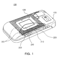
- FIG. 1 is a partially cutaway schematic perspective view showing a of an electronic device, a mobile communications terminal according to an exemplary embodiment of the present invention
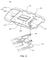
- FIG. 2 is an exploded perspective view of a mobile communications terminal manufactured using an antenna pattern frame according to an exemplary embodiment of the present invention
- FIG. 3 is a schematic perspective view showing an antenna pattern frame according to a first exemplary embodiment of the present invention
- FIG. 4 is an enlarged perspective view showing part A of FIG. 3 according to a first exemplary embodiment of the present invention
- FIG. 5 is an enlarged perspective view showing part A of FIG. 3 according to a second exemplary embodiment of the present invention.
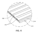
- FIG. 6 is an enlarged perspective view showing part A of FIG. 3 according to a third exemplary embodiment of the present invention.
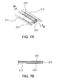
- FIG. 7A is a partially enlarged perspective view of a connection terminal part frame of FIG. 3 ; and FIG. 7B is a cross-sectional view taken along the line VII-VII of FIG. 7A ;
- FIGS. 8A through 8D are schematic perspective views showing operations for manufacturing an antenna pattern frame of FIG. 3 and a case of a mobile communications terminal using the antenna pattern frame;
- FIG. 9 is a schematic perspective view showing an antenna pattern frame according to a second exemplary embodiment of the present invention.
- FIG. 10 is a cross-sectional view taken along line x-x of FIG. 9 ;
- FIGS. 11A and 11B are views showing operations for manufacturing a case of a mobile communications terminal using the antenna pattern frame of FIG. 9 ;
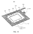
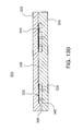
- FIG. 12 is a schematic perspective view showing an antenna pattern frame according to a third exemplary embodiment of the present invention.
- FIGS. 13A through 13D are views showing operations for manufacturing the antenna pattern frame of FIG. 12 ;
- FIGS. 14A and 14B are views showing operations for manufacturing a case of a mobile communications terminal using the antenna pattern frame of FIG. 12 ;
- FIG. 15 is an enlarged perspective view showing part C of FIG. 12 according to a first exemplary embodiment of the present invention.
- FIG. 16 is an enlarged perspective view showing part C of FIG. 12 according to a second exemplary embodiment of the present invention.
- FIG. 17 is a cross-sectional view showing a mold for manufacturing the antenna pattern frame of FIG. 15 ;
- FIG. 18 is a cross-sectional view showing a mold for manufacturing the antenna pattern frame of FIG. 16 ;
- FIG. 19 is a cross-sectional view of a case of a mobile communications terminal manufactured using the antenna pattern frame of FIG. 15 ;
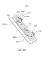
- FIG. 20 is a schematic perspective view showing an antenna pattern frame according to a fourth exemplary embodiment of the present invention.
- FIGS. 21A through 21D are views showing operations for manufacturing the antenna pattern frame of FIG. 19 ;
- FIGS. 22A and 22B are views showing operations for manufacturing a case of a mobile communications terminal using the antenna pattern frame of FIG. 20 ;
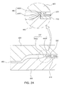
- FIG. 23 is a cross-sectional view showing a modified example of a mold of a case of a mobile communications terminal according to an exemplary embodiment of the present invention.
- FIG. 24 is an enlarged cross-sectional view showing part D of FIG. 23 ;
- FIG. 25 is a cross-sectional view showing a first modified example of part D of FIG. 23 ;
- FIG. 26 is a cross-sectional view showing a second modified example of part D of FIG. 23 ;
- FIG. 27 is a cross-sectional view showing a third modified example of part D of FIG. 23 .
- FIG. 1 is a partially cutaway schematic perspective view showing a partially cutaway case of an electronic device, a mobile communications terminal according to an exemplary embodiment of the present invention
- FIG. 2 is an exploded perspective view of a mobile communications terminal manufactured using an antenna pattern frame according to an exemplary embodiment of the present invention.
- a radiator 220 including an antenna pattern part 222 is embedded in a case 120 of an electronic device, a mobile communications terminal 100 according to an exemplary embodiment of the present invention.
- a radiator frame 210 having the antenna pattern part 222 formed therein is required so that the antenna pattern part 222 may be embedded in the case 120 of the electronic device.
- the mobile communications terminal 100 may be configured to include an antenna pattern frame 200, a case frame 130, and a printed circuit board 140.
- the antenna pattern frame 200 may be fixed to an inner portion of the case frame 130 of the mobile communications terminal 100. Further, as will be described in detail below, the antenna pattern frame 200 may be injection-molded by a mold 400 for the electronic device for manufacturing the case 120 of the electronic device, such that the frame 200 may be integrated with the case frame 130.
- the printed circuit board 140 may be provided with circuit elements that are mounted thereon and that transmit and receive signals to and from the antenna pattern part 222 of the radiator frame 210. Further, a connection wiring 144 connected to a connection terminal part 224 of the antenna pattern frame 200 may be formed on the printed circuit board 140.
- the case 120 of the electronic device may include the radiator frame 210, the radiator 220, and the case frame 130.
- the radiator frame 210 may be formed by injection molding a polymer plastic injection molding liquid.
- the radiator 220 may have the antenna pattern part 222 capable of transmitting or receiving a signal in an appropriate band.
- the case frame 130 may be formed to be injection molded upwardly of the radiator 220, such that the radiator 220 may be embedded between the radiator frame 210 and the case frame 130.
- the radiator frame 210 may be a plate made of plastic, and the plate may have a through hole 240 in the center thereof.
- the antenna pattern part 222 may include a loop antenna wound around an outer portion of the through hole 240.
- a through hole boundary groove 126 may be formed at a boundary between the case frame 130 and the through hole 240.
- the through hole boundary groove 126 may have an inclination, a depth of which becomes shallower in a direction from the through hole 240 toward the case frame 130.
- an outer boundary groove 124 may be formed at a boundary between the case frame 130 formed at an outer portion of the radiator frame 210 and the radiator frame 210.
- the outer boundary groove 124 may have an inclination, a depth of which becomes shallower in a direction from the radiator frame 210 toward the case frame 130 formed at an outer portion of the radiator frame 210.
- a boundary part 122 of the radiator frame 210 including the through hole boundary groove 126 and the outer boundary groove 124 may be formed by boundary jaws 442 and 444 formed in the mold 400 for the case of the electronic device described below as shown in FIGS. 8C and 8D .
- the boundary jaws 442 and 444 may reduce the phenomenon in which a high temperature and high pressure injection molding liquid directly pushes against a bottom surface of a side of the radiator frame 210 disposed in the mold 400 for the case of the electronic device.
- the boundary jaws 442 and 444 may improve flow of the injection molding liquid toward the radiator frame 210, and also weaken an injection molding pressure applied to the radiator frame 210, whereby the antenna pattern frame 200 may be stably disposed within the mold 400 for the case of the electronic device.
- FIG. 3 is a schematic perspective view showing an antenna pattern frame according to a first exemplary embodiment of the present invention
- FIG. 4 is an enlarged perspective view showing part A of FIG. 3 according to a first exemplary embodiment of the present invention
- FIG. 5 is an enlarged perspective view showing part A of FIG. 3 according to a second exemplary embodiment of the present invention
- FIG. 6 is an enlarged perspective view showing part A of FIG. 3 according to a third exemplary embodiment of the present invention
- FIG. 7A is a partially enlarged perspective view of a connection terminal part frame of FIG. 3
- FIG. 7B is a cross-sectional view taken along line VII-VII of FIG. 7A
- FIGS. 8A through 8D are schematic perspective views showing operations for manufacturing an antenna pattern frame of FIG. 3 and a case of a mobile communications terminal using the antenna pattern frame.
- an antenna pattern frame 200 may be provided with the radiator 220 including the antenna pattern part 222 formed by the coating and solidifying of a conductive material on one surface 210a of the radiator frame 210.
- the radiator frame 210 may be a plastic plate formed by injection molding the polymer plastic injection molding liquid, and the plate may have the through hole 240 formed in a center thereof.
- the antenna pattern part 222 may include a loop antenna wound around the outer portion of the through hole 240.
- the radiator 220 may include the connection terminal part 224 formed on a surface 210b opposite to one surface 210a of the radiator frame 210, and a connection part 225 connecting the antenna pattern part 222 to the connection terminal part 224.
- connection terminal part 224 is formed on a connection terminal part support 215 formed to protrude to an outer portion of the radiator frame 210, such that a distance between the connection terminal part 224 and the antenna pattern part 222 may be maintained to be within a predetermined range.
- connection part 225 is formed on a side surface of the radiator frame 210, such that the antenna pattern part 222 and the connection terminal part 224 may be disposed on different planes.
- FIG. 4 is an enlarged cross-sectional view of part A of FIG. 3 .
- the antenna pattern part 222 is applied to and formed on one surface 210a of the flat radiator frame 210.
- FIG. 5 is an enlarged cross-sectional view of part A of FIG. 3 according to a partially modified exemplary embodiment.
- a conductive material is applied to an intaglio position determining groove 212 formed on one surface 210a of the radiator frame 210 to form the antenna pattern part 222.
- FIG. 6 is an enlarged cross-sectional view of part A of FIG. 3 according to another partially modified exemplary embodiment.
- an insulating protective layer 230 providing resistance to the high temperature and high pressure injection molding liquid may be formed.
- an outer circumferential surface of the radiator frame 210 may be provided with an outer jaw 214 formed to be higher than an uppermost portion of the radiator 220.
- the outer jaw 214 may prevent the conductive material from flowing.
- FIGS. 8A through 8D A method of manufacturing an electronic device case having an antenna pattern embedded therein and a mold will be described with reference to FIGS. 8A through 8D .
- a conductive ink is applied to the injection molded radiator frame 210 ( FIG. 8A ) and solidified to form the antenna pattern part 222 ( FIG. 8B ).
- the antenna pattern part may be formed on the radiator frame 210 by at least one of a sputtering method, a printing method, a plating method, a stamping method, a drawing method, and a dispensing method.
- FIG. 8B shows the antenna pattern part formed on the radiator frame 210 by an inkjet printing method using the conductive ink thereon.
- the antenna pattern part 222 may be formed on the position determining groove 212 ( FIG. 5 ) formed on the radiator frame 210, and the insulating protective layer 230 for protecting the antenna pattern part 222 from high temperature and high pressure injection molding conditions may be formed on the antenna pattern part 222.
- the radiator frame 210 may be molded so that the through hole 240 is formed at a center of the antenna pattern part 222.
- the outer circumferential surface of the radiator frame 210 manufactured as described above may be inserted into and seated in an inner side of a boundary part forming part formed at the mold 400 for the case of the electronic device as shown in FIG. 8C .
- the boundary part forming part which is the boundary jaw formed to protrude from the mold 400 for the case of the electronic device, may include an inner boundary jaw 444 having the through hole 240 of the radiator frame 210 inserted thereinto and an outer boundary jaw 442 having an outer circumferential portion of the radiator frame 210 inserted thereinto.
- a resin material is introduced from an outer side of the boundary part forming part, passes through the boundary part forming part, is introduced from an upper surface of the radiator frame 210 and then fills an inner space 450 having a shape of the case frame 130 formed in the mold 400 for the case of the electronic device as shown in FIG. 8D .
- the mold 400 for the case of the electronic device will be described with reference to FIGS. 8C and 8D .
- the mold 400 for the case of the electronic device may include an upper mold 420 and a lower mold 440.
- the radiator frame 210 may be in contact with and be supported by the upper mold 420 and the lower mold 440, the radiator frame 210 having the radiator 220 coated and solidified with the conductive material.
- a resin material inlet 460 may be formed in the upper mold, the lower mold, or the upper and lower molds 420 and 440 so that the case frame shaped inner space 450 formed by combining the upper and lower molds 420 and 440 becomes the case frame 130.
- At least one of the upper and lower molds 420 and 440 may be provided with the boundary part forming part into which the radiator frame 210 is inserted.
- the boundary part forming part may be a protrusion protruding from the upper mold or the lower mold so that an outer circumferential portion defining an outer boundary of the radiator frame 210 and an inner circumferential portion of the through hole 240 formed in the radiator frame 210 are inserted thereinto.
- the protrusion may include the outer boundary jaw 442 and the inner boundary jaw 444.
- the boundary part forming part may have an increasing inclination in a direction in which the resin material moves in the inner space 450, and may have an inclination through which the introduced resin material first may first contact the upper surface of the radiator frame 210.
- the height of the boundary part forming part may be reduced in a direction from a boundary part of the radiator frame 210 toward the inner space thereof.
- antenna pattern part 222 made of the conductive material formed on the surface of the radiator frame 210 is pushed or peeled off during the injection molding, antenna characteristics may change. Therefore, caution is required therewith.
- the resin material inlet 460 may be disposed away from the antenna pattern part 222 in the range that does not cause a defect in the injection molding at an outer portion of the boundary part forming part.
- FIG. 9 is a schematic perspective view showing an antenna pattern frame according to a second exemplary embodiment of the present invention
- FIG. 10 is a cross-sectional view taken along line X-X of FIG. 9
- FIGS.11A and 11B are views showing operations for manufacturing a case of a mobile communications terminal using the antenna pattern frame of FIG. 9 .
- FIGS. 9 through 11 An antenna pattern frame used for manufacturing an electronic device case by double injection molding according to a second exemplary embodiment will be described with reference to FIGS. 9 through 11 .
- content different from that of the antenna pattern frame according to the first exemplary embodiment will be described, and content other than the content described below is referred to the content described in the antenna pattern frame according to the first exemplary embodiment.
- the antenna pattern frame 200 may include the radiator frame 210 injection molded so that the radiator 220 including the antenna pattern part 222 formed of a metal sheet is exposed on one surface 210a thereof, rather than injection molding the radiator frame 210 using the polymer plastic and then coating thereon with the conductive material.
- the radiator 220 may include the antenna pattern part 222 formed by press processing the metal sheet.
- the radiator 220 may include the connection terminal part 224 formed on one surface 210a of the radiator frame 210, and the connection terminal part 224 may be embedded in and exposed from the connection terminal part support 215 formed to protrude to the outer portion of the radiator frame 210.
- connection terminal part 224 formed at the connection terminal part support 215 may be provided with an interconnection hole 218 into which a connection pin 148 of the printed circuit board 140 ( FIG. 2 ) of the electronic device is inserted.
- the antenna pattern frame 200 as described above may be inserted into a boundary part forming part formed in an inner portion of a mold 400 substantially the same as the mold 400 for manufacturing the case of the electronic device using the antenna pattern frame according to the first exemplary embodiment of the present invention.
- the case 120 of the electronic device may be manufactured by introducing an injection molding liquid into the inner space 450 of the mold 400 for the electronic device case.
- the boundary part forming part may prevent the antenna pattern frame from being moved within the mold 400 for the electronic device case.
- FIG. 12 is a schematic perspective view showing an antenna pattern frame according to a third exemplary embodiment of the present invention
- FIGS. 13A through 13D are views showing operations for manufacturing the antenna pattern frame of FIG. 12
- FIGS. 14A and 14B are views showing operations for manufacturing a case of a mobile communications terminal using the antenna pattern frame of FIG. 12
- FIG. 15 is an enlarged perspective view showing part C of FIG. 12 according to a first exemplary embodiment of the present invention
- FIG. 16 is an enlarged perspective view showing part C of FIG. 12 according to a second exemplary embodiment of the present invention.
- FIG. 17 is a cross-sectional view schematically showing a mold for manufacturing the antenna pattern frame of FIG. 15 ;
- FIG. 18 is a cross-sectional view schematically showing a mold for manufacturing the antenna pattern frame of FIG. 16 ;
- FIG. 19 is a cross-sectional view of a case of a mobile communications terminal manufactured using the antenna pattern frame of FIG. 15 .
- FIGS. 12 through 19 An antenna pattern frame used for manufacturing an electronic device case manufactured by double injection molding according to a third exemplary embodiment will be described with reference to FIGS. 12 through 19 .
- content other than the content described below is referred to the content described in the antenna pattern frame according to the first exemplary embodiment.
- the antenna pattern frame 200 may include the radiator frame 210 injection molded so that the radiator 220 including the antenna pattern part 222 and formed on a film 250 is formed on one surface 210a thereof.
- the antenna pattern is formed on the film 250, whereby a thin and elongate antenna pattern may be easily implemented, as compared to a case of using the metal sheet.
- the radiator frame 210 may include the through hole 240, and the antenna pattern part 222 may include the loop antenna wound around the outer portion of the through hole 240.
- the antenna pattern part 222 may include an antenna coil wound multiple times so that the low frequency signal may be transmitted or received.
- the antenna pattern part 222 may include the antenna coil, whereby a small electronic apparatus such as the mobile communications terminal may also transmit or receive a broadcasting frequency in a low frequency band without a separate exterior antenna and may perform RFID communication.
- the low frequency antenna pattern part may also be used as a wireless charging type antenna pattern.
- the case of the electronic device having the above-mentioned low frequency antenna pattern embedded therein may also be manufactured by double injection molding.
- the radiator 220 including the low frequency antenna pattern part may be formed of a thin and elongate antenna pattern, and may be formed by coating the conductive material on the film 250.
- this metal pattern may also be used as the low frequency antenna pattern part.
- the radiator frame 210 may be injection molded using a polymer mixture containing a magnetic substance component so that the radiator 220 including the low frequency antenna pattern part 222 is formed on one surface 210a thereof.
- a capacitive component is generated around the radiator 220 by changing the permittivity of the material of the radiator frame 210 as a base on which the radiator 220 is mounted, such that a length of the antenna pattern may be reduced.
- a length of the antenna pattern is reduced as described above, a size of the radiator frame 210 may be reduced.
- the radiator frame 210 of the low frequency antenna pattern part 222 also may have the through hole 240, and the antenna pattern part 222 may include the antenna coil wound multiple times around the outer portion of the through hole 240.
- the polymer mixture containing the magnetic substance component includes a magnetic substance component having high permeability such as ferrite, whereby performance of the low frequency band antenna may be improved and noise, electromagnetic wave, and the like, generated during operation of an set apparatus may be efficiently shielded.
- the radiator frame 210 including the above-mentioned low frequency antenna pattern part 222 formed on one surface 210a thereof and made of the polymer mixture containing the magnetic substance component is seated in the mold 400 for the case of the electronic device, and the injection molding liquid is introduced thereinto, whereby the low frequency antenna pattern part 222 may be embedded between the radiator frame 210 and the case frame 130.
- the case frame 130 may be formed by injection molding an injection molding liquid of at least one selected from a polycarbonate (PC), an acrylonitrile-butadiene-styrene (ABS), a resin and a polymer plastic.
- PC polycarbonate
- ABS acrylonitrile-butadiene-styrene
- resin a polymer plastic
- a film type antenna pattern frame 200 may be manufactured by inserting the film 250 having the antenna pattern part 222 formed thereon through a manufacturing process of FIGS. 13A through 13D into a mold 300 of the antenna pattern frame.
- the film 250 have the antenna pattern part 222 formed thereon may be adhered to an upper mold 320 of the mold 300 of the antenna pattern frame or may be supported by and fixed to a moving pin 342, or the like.
- a lower mold 340 may be provided with the moving pin 342, a through hole forming part 348 having a shape corresponding to the through hole 240 of the radiator frame 210, an interconnection hole forming pine 344, or the like.
- the resin is filled in an inner space 350 having the shape of the radiator frame 210 formed by combining the upper mold 320 and the lower mold 340, whereby the radiator frame 210 to which the film 250 having the antenna pattern part 222 formed thereon is injection molded and fixed may be formed.
- the film 250 may be made of a polymer plastic material containing a Cu component.
- the polymer plastic material may be of a polycarbonate (PC), a polyethylene terephthalate (PET), an acrylonitrile-butadiene-styrene (ABS), a mixture thereof, and the like.
- a process for forming the antenna pattern part 222 on the film 250 may use not only a method of pressing and adhering a metal sheet but also a sputtering method, a printing method, a plating method, a stamping method, a drawing method, a dispensing method, and the like, on the film 250.
- a method of applying the conductive material rather than pressing and adhering the metal sheet may be used for forming the thin and elongate antenna pattern.
- the above-mentioned antenna pattern frame 200 is inserted into the mold 400 for the case of the electronic device as shown in FIG. 14A , and the resin material is introduced thereinto as shown in FIG. 14B , whereby, the case 120 of the electronic device may be formed.
- a description of the mold and the method of manufacturing the case of the electronic device may be replaced with the description in FIGS. 8C and 8D .
- FIGS. 15 and 16 show a modified example of part C of the antenna pattern frame 200 of FIG. 12 .
- the radiator frame 210 may include an over-mold part 217 formed to cover a portion of each of adjacent antenna pattern parts 222.
- the radiator frame 210 may include an over-mold part 217 formed to cover all antenna pattern parts 222 adjacent thereto.
- the over-mold part 217 serves to prevent the antenna pattern part 222 from being loose on the radiator frame 210 and firmly fix the antenna pattern part 222 to the radiator frame 210.
- the mold 300 of the antenna pattern frame of FIGS. 17 and 18 may be used to manufacture the antenna pattern frame 200 of FIGS. 15 and 16 .
- the upper mold 320 of the mold 300 of the antenna pattern frame has an over-mold part forming groove 322 formed therein, wherein the upper mold 320 contacts the film 250 including the antenna pattern part 222.
- FIG. 19 is a cross-sectional view of the case 120 of the electronic device including the case frame 130 manufactured by double injection molding the antenna pattern frame 200 including the over-mold part 217.
- a resin material used during secondary injection molding a resin material having a temperature at which surfaces of the over-moldpart 217 and the radiator frame 210 may be melted may be used.
- FIG. 20 is a schematic perspective view showing an antenna pattern frame according to a fourth exemplary embodiment of the present invention
- FIGS. 21A through 21D are views showing operations of manufacturing the antenna pattern frame of FIG. 19
- FIGS. 22A and 22B are views showing operations for manufacturing a case of a mobile communications terminal using the antenna pattern frame of FIG. 20 .
- An antenna pattern frame 200 according to the present embodiment is the same in a basic idea as the antenna pattern frame 200 according to the third exemplary embodiment in that the antenna pattern part 222 is fixed using the film 250.
- the antenna pattern frame 200 according to the present embodiment has a difficulty in being used as an antenna for low frequency communication in that a plurality of radiators 220a and 220b formed by pressing the metal sheet are fixed onto the film as shown in FIG. 21A .
- the plurality of radiators 220a and 220b are fixed onto the film 250 by a method such as an adhesion method, or the like as shown in FIG. 21B .
- the film 250 has pin holes 252 formed therein, and the pin hole 252 may be inserted and fixed into a contact pin 346, or the like, formed in the mold 300 of the antenna pattern frame to thereby prevent the antenna pattern frame 200 from being moved during the introduction of the injection molding liquid.
- the antenna pattern frame 200 manufactured as described above is the same as the antenna pattern frame described in FIGS. 8C and 8D in that the antenna pattern frame 200 inserted into the boundary part forming part 442 of the mold 400 for the case of the electronic device and is injection molded as shown in FIGS. 22A and 22B .
- FIG. 23 is a cross-sectional view showing a modified example of a mold of a case of a mobile communications terminal according to an exemplary embodiment of the present invention
- FIG. 24 is an enlarged cross-sectional view schematically showing part D of FIG. 23
- FIG. 25 is a cross-sectional view schematically showing a first modified example of part D of FIG. 23
- FIG. 26 is a cross-sectional view schematically showing a second modified example of part D of FIG. 23
- FIG. 27 is a cross-sectional view schematically showing a third modified example of part D of FIG. 23 .
- FIGS. 23 through 26 show a mold 400 of a case of an electronic device to which the antenna pattern frame 200 according to the first exemplary embodiment is applied.
- antenna pattern frames 200 may be applied to modified examples of a mold of a case of an electronic device described below.
- the outer boundary jaw 442 defining the outer boundary of the radiator frame 210 may include an inclination part 4422 guiding an injection molding product to be inclined upwardly or downwardly within the case frame shaped inner space 450 and a flat part 4424 guiding the injection molding product upward of the radiator frame 210 horizontally.
- the inclination part 4422 of the outer boundary jaw 442 may have a tangential gradient of a bottom surface increased or decreased in a moving direction of the injection molding liquid.
- the outer boundary jaw 442 close to the resin material inlet 460 may have a tangential gradient of a bottom surface increased in the moving direction of the injection molding liquid, and the outer boundary jaw 442 shown in FIG. 23 distant from the resin material inlet 460 may have a tangential gradient of a bottom surface decreased in the moving direction of the injection molding liquid.
- FIG. 25 a modified example of a mold 400 for a case of an electronic device in which a height H 2 of the radiator frame 210 corresponds to a height H 1 of the flat part 4424 of the outer boundary jaw 442 is shown.
- the height H 2 of the radiator frame 210 is the same as the height H 1 of the flat part 4424 of the outer boundary jaw 442 as described above, a vortex phenomenon due to a direction conversion of the injection molding liquid in the case frame shaped inner space 450 may be reduced.
- FIG. 26 unlike the example of FIGS. 23 and 24 , a modified example of a mold 400 for an electronic device case including the outer boundary jaw 442 without the flat part 4424 is shown.
- a height of the outer boundary jaw 442 may correspond to that of the radiator frame 210.
- FIG. 27 unlike the example of FIGS. 23 and 24 , an inclination part of the outer boundary jaw 442 having a sine wave shape is shown.
- a tangential gradient ⁇ 1 of a bottom surface of the outer boundary jaw 442 may be increased and then decreased to a tangential gradient ⁇ 2, based on the outer boundary jaw 442 close to the resin material inlet 460.
- This structure may reduce resistance of movement of the injection molding product.
- the height of the outer boundary jaw 442 may correspond to that of the radiator frame 210.
- the shapes of the antenna pattern part and the connection terminal part or the method of manufacturing the same, and the mold as described above, may be appropriately combined with the methods described in other exemplary embodiments according to the purpose of the frequency band.
- the radiator having the antenna pattern part formed therein may be embedded in the case of the electronic device, whereby defects, such as vulnerability to external impacts in the case of the exterior type antenna according to the related art, and an increase in product volume in the case of the interior type antenna according to the related art may be solved.
- the low frequency antenna may be implemented in a miniaturized electronic device, whereby low frequency broadcasting may be received without a separate exterior antenna in a small apparatus and the low frequency antenna may be variously applied as an antenna for radio frequency identification (RFID) communication, a wireless charging type antenna, and the like.
- RFID radio frequency identification
- the antenna pattern frame is not moved or deformed within the mold of the case of the electronic device in which the injection molding is performed at a high temperature and at a high pressure, whereby a rate of defectivity in an appearance may be reduced and the performance of the antenna may be improved.
- the antenna film is not adhered to the outer surface of the case, whereby the defect in which an antenna film is separated from the case due to the elasticity of the antenna film itself may be solved.
- the antenna pattern frame may be applied to all electronic devices requiring an antenna by manufacturing a case of the electronic device having the antenna pattern part embedded therein, whereby the antenna pattern frame may be variously applied.
Landscapes
- Engineering & Computer Science (AREA)
- Manufacturing & Machinery (AREA)
- Mechanical Engineering (AREA)
- Computer Networks & Wireless Communication (AREA)
- Physics & Mathematics (AREA)
- Electromagnetism (AREA)
- Details Of Aerials (AREA)
- Telephone Set Structure (AREA)
- Support Of Aerials (AREA)
- Injection Moulding Of Plastics Or The Like (AREA)
- Moulds For Moulding Plastics Or The Like (AREA)
Applications Claiming Priority (2)
| Application Number | Priority Date | Filing Date | Title |
|---|---|---|---|
| KR20100044185 | 2010-05-11 | ||
| KR1020110007346A KR101179363B1 (ko) | 2010-05-11 | 2011-01-25 | 안테나 패턴 프레임이 매립되는 전자장치의 케이스, 이의 제조금형 및 제조방법 |
Publications (1)
| Publication Number | Publication Date |
|---|---|
| EP2386400A1 true EP2386400A1 (fr) | 2011-11-16 |
Family
ID=44343977
Family Applications (1)
| Application Number | Title | Priority Date | Filing Date |
|---|---|---|---|
| EP11250429A Withdrawn EP2386400A1 (fr) | 2010-05-11 | 2011-04-05 | Boîtier de dispositif électronique doté d'un cadre de motif d'antenne intégré, moule correspondant et son procédé de fabrication |
Country Status (4)
| Country | Link |
|---|---|
| US (1) | US9266266B2 (fr) |
| EP (1) | EP2386400A1 (fr) |
| JP (1) | JP5321988B2 (fr) |
| CN (1) | CN102244992B (fr) |
Families Citing this family (16)
| Publication number | Priority date | Publication date | Assignee | Title |
|---|---|---|---|---|
| WO2010068072A2 (fr) * | 2008-12-11 | 2010-06-17 | Ma Sang-Yong | Module d'antenne pour un terminal portatif dans lequel une antenne est insérée et procédé de fabrication de ce module d'antenne |
| EP2386401A1 (fr) * | 2010-05-11 | 2011-11-16 | Samsung Electro-Mechanics Co., Ltd. | Boîtier de dispositif électronique doté d'un motif d'antenne intégré, moule correspondant et son procédé de fabrication |
| EP2386400A1 (fr) | 2010-05-11 | 2011-11-16 | Samsung Electro-Mechanics Co., Ltd. | Boîtier de dispositif électronique doté d'un cadre de motif d'antenne intégré, moule correspondant et son procédé de fabrication |
| JP5305113B2 (ja) | 2010-05-11 | 2013-10-02 | サムソン エレクトロ−メカニックス カンパニーリミテッド. | 低周波用アンテナパターンが埋め込まれる電子装置ケース、その製造金型及び製造方法 |
| KR101219004B1 (ko) * | 2011-05-09 | 2013-01-21 | 삼성전기주식회사 | 통신 단말기 및 그 제조 방법 |
| US9246214B2 (en) * | 2012-03-08 | 2016-01-26 | Apple Inc. | Electronic device antenna structures with ferrite layers |
| KR101931636B1 (ko) * | 2012-05-16 | 2018-12-21 | 엘지이노텍 주식회사 | 통신 단말의 안테나 및 그 제조 방법 |
| KR101952852B1 (ko) * | 2013-06-28 | 2019-02-27 | 삼성전기주식회사 | 안테나 패턴이 매립되는 방사체 프레임, 이를 포함하는 안테나 패턴 프레임 및 이를 포함하는 전자장치 |
| US20150048994A1 (en) * | 2013-08-19 | 2015-02-19 | Dae San Electronics Co., Ltd. | Antenna module and manufacturing method thereof |
| KR20150021419A (ko) * | 2013-08-20 | 2015-03-02 | 삼성전기주식회사 | 안테나 모듈 및 이를 포함하는 전자 장치 |
| EP2992776B1 (fr) * | 2014-09-04 | 2019-11-06 | WITS Co., Ltd. | Boîtier et appareil le comprenant |
| CN105530783B (zh) * | 2014-12-26 | 2016-10-12 | 比亚迪股份有限公司 | 一种通讯设备金属外壳及其制备方法 |
| KR101609642B1 (ko) * | 2015-07-10 | 2016-04-08 | 주식회사 아모그린텍 | Nfc 안테나 일체형 방열시트 및 이를 구비하는 휴대단말기 |
| JP6453195B2 (ja) * | 2015-09-29 | 2019-01-16 | 日立オートモティブシステムズ株式会社 | 車載制御装置 |
| EP3598571B1 (fr) * | 2018-07-17 | 2021-10-06 | LS Mtron Ltd. | Module d'antenne et?son procédé de fabrication |
| US11139552B1 (en) | 2020-05-05 | 2021-10-05 | Semiconductor Components Industries, Llc | Method of forming a semiconductor device |
Citations (14)
| Publication number | Priority date | Publication date | Assignee | Title |
|---|---|---|---|---|
| JPS5820418A (ja) * | 1981-07-30 | 1983-02-05 | Toyoda Gosei Co Ltd | インサ−ト成形方法 |
| JPS61268415A (ja) * | 1985-05-23 | 1986-11-27 | Ryoden Kasei Co Ltd | 樹脂成形体の製造方法 |
| JPS62221521A (ja) * | 1986-03-25 | 1987-09-29 | Toyoda Gosei Co Ltd | インサ−ト成形方法 |
| US4944087A (en) * | 1988-10-05 | 1990-07-31 | Rogers Corporation | Method of making a curved plastic body with circuit pattern |
| JPH0788888A (ja) * | 1993-09-24 | 1995-04-04 | Inoac Corp | モール端末の成形方法 |
| JPH08276458A (ja) * | 1995-04-06 | 1996-10-22 | Dainippon Printing Co Ltd | 非接触icタグの製造方法及び非接触icタグ |
| FR2806343A1 (fr) * | 2000-03-16 | 2001-09-21 | Markage | Procede de protection d'une etiquette electronique par surmoulage |
| US20060216469A1 (en) * | 2000-12-29 | 2006-09-28 | Kenichi Hashizume | Method for manufacturing a resin injection molded article with a reinforcing or decorative core |
| EP1783858A1 (fr) * | 2005-10-28 | 2007-05-09 | Hirschmann Car Communication GmbH | Feuille de support comprenant des structures d'antennes et évidements et/ou perforations et/ou marques |
| US20070216580A1 (en) * | 2006-03-15 | 2007-09-20 | Chant Sincere Co., Ltd. | Electro-stimulating massage confiner |
| US20080067715A1 (en) * | 2006-09-15 | 2008-03-20 | Samsung Electro-Mechanics Co., Ltd. | Method of manufacturing case structure having antenna |
| JP2008226099A (ja) * | 2007-03-15 | 2008-09-25 | Dainippon Printing Co Ltd | 非接触式データキャリア装置 |
| KR100910161B1 (ko) * | 2009-02-25 | 2009-07-30 | 주식회사 에이티앤씨 | 내장형 안테나 일체형 휴대단말기 케이스 및 그 제조 방법 |
| KR100932079B1 (ko) * | 2009-03-31 | 2009-12-15 | 마상영 | 휴대 단말기용 인서트 안테나모듈 및 그 제조방법 |
Family Cites Families (35)
| Publication number | Priority date | Publication date | Assignee | Title |
|---|---|---|---|---|
| JP2652119B2 (ja) * | 1993-01-18 | 1997-09-10 | 日本写真印刷株式会社 | 成形同時絵付金型および成形同時絵付品の製造方法 |
| JPH06253910A (ja) | 1994-02-25 | 1994-09-13 | Seiko Epson Corp | 電極導体内蔵バンドの製造方法 |
| GB2345196B (en) | 1998-12-23 | 2003-11-26 | Nokia Mobile Phones Ltd | An antenna and method of production |
| JP2001277287A (ja) * | 2000-03-31 | 2001-10-09 | Nissha Printing Co Ltd | 部分加飾成形品とその製造方法 |
| US6486837B2 (en) * | 2001-04-09 | 2002-11-26 | Molex Incorporated | Antenna structures |
| JP2002344221A (ja) * | 2001-04-27 | 2002-11-29 | Molex Inc | ヘリカルアンテナとその製造方法 |
| US20030098814A1 (en) * | 2001-11-09 | 2003-05-29 | Keller Walter John | Multiband antenna formed of superimposed compressed loops |
| JP2003158415A (ja) * | 2001-11-20 | 2003-05-30 | Ntn Corp | 無線通信機能付き機器 |
| US20050236110A1 (en) | 2001-11-27 | 2005-10-27 | Bhatt Sanjiv M | Semiconductor component handling device having a performance film |
| JP3907045B2 (ja) * | 2002-03-01 | 2007-04-18 | ソニー・エリクソン・モバイルコミュニケーションズ株式会社 | 携帯通信端末 |
| JP4854702B2 (ja) * | 2003-08-29 | 2012-01-18 | 富士通テン株式会社 | アンテナ |
| JP2005277607A (ja) | 2004-03-23 | 2005-10-06 | Sony Corp | アンテナモジュール用磁芯部材の製造方法およびその製造用金型 |
| JP2005333244A (ja) | 2004-05-18 | 2005-12-02 | Mitsubishi Electric Corp | 携帯電話機 |
| JP2005341027A (ja) * | 2004-05-25 | 2005-12-08 | Nec Saitama Ltd | 携帯通信端末及びその形成方法 |
| JP2006339757A (ja) | 2005-05-31 | 2006-12-14 | Denso Corp | アンテナコイル、通信基板モジュールの製造方法及びカード型無線機 |
| JPWO2007000807A1 (ja) * | 2005-06-28 | 2009-01-22 | 富士通株式会社 | 無線周波数識別タグ |
| DE102006033192A1 (de) | 2005-08-18 | 2007-03-29 | Samsung Electro-Mechanics Co., Ltd., Suwon | Eingebautes Antennenmodul eines kabellosen Kommunikationsendgeräts |
| JP2007116347A (ja) | 2005-10-19 | 2007-05-10 | Mitsubishi Materials Corp | タグアンテナ及び携帯無線機 |
| KR100816262B1 (ko) | 2005-10-24 | 2008-03-26 | 주식회사 이엠따블유안테나 | 전자 기기 하우징 내장형 안테나 및 그 제조방법 |
| CN101043098A (zh) | 2006-03-23 | 2007-09-26 | 广达电脑股份有限公司 | 改善损耗性介质对天线影响的通讯电子装置 |
| KR100843424B1 (ko) * | 2006-07-06 | 2008-07-03 | 삼성전기주식회사 | 스퍼터링 공정을 이용한 필름형 안테나 제조 방법 |
| CN101114731B (zh) | 2006-07-26 | 2012-01-04 | 佳邦科技股份有限公司 | 图形化的天线结构 |
| KR100764757B1 (ko) | 2006-09-04 | 2007-10-08 | 주식회사 미래산업 | 모바일 단말기용 케이스 및 그 제조 방법 |
| JP2008205557A (ja) * | 2007-02-16 | 2008-09-04 | Matsushita Electric Ind Co Ltd | アンテナ装置 |
| FR2914113B1 (fr) * | 2007-03-20 | 2009-05-01 | Trixell Soc Par Actions Simpli | Antenne mixte |
| KR20090006336A (ko) | 2007-07-11 | 2009-01-15 | 삼성전기주식회사 | 케이스 일체형 안테나 및 그 제조방법 |
| JP4881247B2 (ja) * | 2007-07-13 | 2012-02-22 | 株式会社東芝 | 電子機器及びその製造方法 |
| KR100872286B1 (ko) * | 2007-08-22 | 2008-12-05 | 삼성전기주식회사 | 도전패턴이 형성된 케이스 구조물 및 그 제조방법 |
| KR101545019B1 (ko) | 2007-09-05 | 2015-08-18 | 삼성전자주식회사 | Lds를 이용한 전자 기기의 제조방법 및 그에 의해 제조된 전자 기기 |
| CN101442149B (zh) | 2007-11-23 | 2012-09-19 | 鸿富锦精密工业(深圳)有限公司 | 电子设备及卡扣装置 |
| CN201234285Y (zh) | 2008-07-15 | 2009-05-06 | 比亚迪股份有限公司 | 信息卡固定装置及具有其的移动通信装置 |
| KR100930207B1 (ko) | 2009-03-16 | 2009-12-07 | 삼성전기주식회사 | 이동통신 단말기 케이스 제조방법, 이를 이용한 이동통신 단말기 케이스 및 이동통신 단말기 |
| KR100945117B1 (ko) | 2009-04-23 | 2010-03-02 | 삼성전기주식회사 | 안테나 패턴 프레임 및 그 제조방법 |
| KR100935954B1 (ko) | 2009-04-23 | 2010-01-12 | 삼성전기주식회사 | 전자장치 케이스, 그 제조방법 및 제조금형, 이동통신 단말기 |
| EP2386400A1 (fr) | 2010-05-11 | 2011-11-16 | Samsung Electro-Mechanics Co., Ltd. | Boîtier de dispositif électronique doté d'un cadre de motif d'antenne intégré, moule correspondant et son procédé de fabrication |
-
2011
- 2011-04-05 EP EP11250429A patent/EP2386400A1/fr not_active Withdrawn
- 2011-04-05 JP JP2011083549A patent/JP5321988B2/ja not_active Expired - Fee Related
- 2011-05-03 US US13/099,930 patent/US9266266B2/en not_active Expired - Fee Related
- 2011-05-11 CN CN201110124913.0A patent/CN102244992B/zh not_active Expired - Fee Related
Patent Citations (14)
| Publication number | Priority date | Publication date | Assignee | Title |
|---|---|---|---|---|
| JPS5820418A (ja) * | 1981-07-30 | 1983-02-05 | Toyoda Gosei Co Ltd | インサ−ト成形方法 |
| JPS61268415A (ja) * | 1985-05-23 | 1986-11-27 | Ryoden Kasei Co Ltd | 樹脂成形体の製造方法 |
| JPS62221521A (ja) * | 1986-03-25 | 1987-09-29 | Toyoda Gosei Co Ltd | インサ−ト成形方法 |
| US4944087A (en) * | 1988-10-05 | 1990-07-31 | Rogers Corporation | Method of making a curved plastic body with circuit pattern |
| JPH0788888A (ja) * | 1993-09-24 | 1995-04-04 | Inoac Corp | モール端末の成形方法 |
| JPH08276458A (ja) * | 1995-04-06 | 1996-10-22 | Dainippon Printing Co Ltd | 非接触icタグの製造方法及び非接触icタグ |
| FR2806343A1 (fr) * | 2000-03-16 | 2001-09-21 | Markage | Procede de protection d'une etiquette electronique par surmoulage |
| US20060216469A1 (en) * | 2000-12-29 | 2006-09-28 | Kenichi Hashizume | Method for manufacturing a resin injection molded article with a reinforcing or decorative core |
| EP1783858A1 (fr) * | 2005-10-28 | 2007-05-09 | Hirschmann Car Communication GmbH | Feuille de support comprenant des structures d'antennes et évidements et/ou perforations et/ou marques |
| US20070216580A1 (en) * | 2006-03-15 | 2007-09-20 | Chant Sincere Co., Ltd. | Electro-stimulating massage confiner |
| US20080067715A1 (en) * | 2006-09-15 | 2008-03-20 | Samsung Electro-Mechanics Co., Ltd. | Method of manufacturing case structure having antenna |
| JP2008226099A (ja) * | 2007-03-15 | 2008-09-25 | Dainippon Printing Co Ltd | 非接触式データキャリア装置 |
| KR100910161B1 (ko) * | 2009-02-25 | 2009-07-30 | 주식회사 에이티앤씨 | 내장형 안테나 일체형 휴대단말기 케이스 및 그 제조 방법 |
| KR100932079B1 (ko) * | 2009-03-31 | 2009-12-15 | 마상영 | 휴대 단말기용 인서트 안테나모듈 및 그 제조방법 |
Also Published As
| Publication number | Publication date |
|---|---|
| CN102244992A (zh) | 2011-11-16 |
| JP2011239366A (ja) | 2011-11-24 |
| US20110279333A1 (en) | 2011-11-17 |
| JP5321988B2 (ja) | 2013-10-23 |
| US9266266B2 (en) | 2016-02-23 |
| CN102244992B (zh) | 2015-08-26 |
Similar Documents
| Publication | Publication Date | Title |
|---|---|---|
| US8711041B2 (en) | Case of electronic device having antenna pattern embedded therein and mold and method for manufacturing the same | |
| US9266266B2 (en) | Case of electronic device having antenna pattern frame embedded therein, mold therefor and method of manufacturing thereof | |
| EP2387106B1 (fr) | Boîtier de dispositif électronique doté d'un motif d'antenne basse fréquence intégré, moule correspondant et son procédé de fabrication | |
| US9419326B2 (en) | Antenna pattern frame, method and mold for manufacturing the same, method for manufacturing an electronic device case, and electronic device | |
| US8933844B2 (en) | Antenna pattern frame, electronic device case provided with antenna pattern frame and electronic device including electronic device case | |
| US20110291899A1 (en) | Antenna radiator, method of manufacturing electronic device case having plurality of antenna pattern radiators embedded therein, and electronic device case | |
| US20110222219A1 (en) | Electronic device case, mold for manufacturing the same, and mobile communications terminal | |
| CN101587985A (zh) | 膜式天线和移动通信终端 | |
| KR101179306B1 (ko) | 안테나 패턴이 매립되는 전자장치의 케이스, 이의 제조금형 및 제조방법 | |
| KR101179362B1 (ko) | 저주파용 안테나 패턴이 매립되는 전자장치의 케이스, 이의 제조금형 및 제조방법 | |
| EP2520406A2 (fr) | Terminal de communication et son procédé de fabrication | |
| US9531066B2 (en) | Antenna pattern frame and electronic device including the same | |
| KR20130051054A (ko) | 안테나 모듈이 내장되는 무선통신기기 케이스 및 이의 제조방법 | |
| KR101133314B1 (ko) | 안테나 패턴이 매립되는 전자장치의 케이스, 이의 제조금형 및 제조방법 | |
| KR101179363B1 (ko) | 안테나 패턴 프레임이 매립되는 전자장치의 케이스, 이의 제조금형 및 제조방법 | |
| KR101651903B1 (ko) | 안테나 구조체 및 그 제조 방법 | |
| KR20120059828A (ko) | 연성인쇄회로기판 및 이의 제조 방법 | |
| KR20160046766A (ko) | 안테나 구조체 | |
| KR20160030594A (ko) | 안테나 패턴을 구비하는 방사체 프레임 및 그 제조방법 |
Legal Events
| Date | Code | Title | Description |
|---|---|---|---|
| 17P | Request for examination filed |
Effective date: 20110428 |
|
| AK | Designated contracting states |
Kind code of ref document: A1 Designated state(s): AL AT BE BG CH CY CZ DE DK EE ES FI FR GB GR HR HU IE IS IT LI LT LU LV MC MK MT NL NO PL PT RO RS SE SI SK SM TR |
|
| AX | Request for extension of the european patent |
Extension state: BA ME |
|
| PUAI | Public reference made under article 153(3) epc to a published international application that has entered the european phase |
Free format text: ORIGINAL CODE: 0009012 |
|
| RIN1 | Information on inventor provided before grant (corrected) |
Inventor name: JEON, DAE SEONG Inventor name: LEE, DUK WOO Inventor name: HONG, HA RYONG Inventor name: HAN, CHANG MOK Inventor name: SUNG, JAE SUK Inventor name: CHANG, KI WON Inventor name: LEE, DAE KYU Inventor name: AN, CHAN GWANG Inventor name: CHO, SUNG EUN |
|
| RIN1 | Information on inventor provided before grant (corrected) |
Inventor name: LEE, DAE KYU Inventor name: HONG, HA RYONG Inventor name: LEE, DUK WOO Inventor name: CHO, SUNG EUN Inventor name: SUNG, JAE SUK Inventor name: AN, CHAN GWANG Inventor name: HAN, CHANG MOK Inventor name: JEON, DAE SEONG Inventor name: CHANG, KI WON |
|
| 17Q | First examination report despatched |
Effective date: 20151007 |
|
| GRAP | Despatch of communication of intention to grant a patent |
Free format text: ORIGINAL CODE: EPIDOSNIGR1 |
|
| INTG | Intention to grant announced |
Effective date: 20160620 |
|
| RAP1 | Party data changed (applicant data changed or rights of an application transferred) |
Owner name: SAMSUNG ELECTRO-MECHANICS CO., LTD. |
|
| STAA | Information on the status of an ep patent application or granted ep patent |
Free format text: STATUS: GRANT OF PATENT IS INTENDED |
|
| STAA | Information on the status of an ep patent application or granted ep patent |
Free format text: STATUS: THE APPLICATION IS DEEMED TO BE WITHDRAWN |
|
| 18D | Application deemed to be withdrawn |
Effective date: 20161101 |