EP2386114B1 - Scatterometry metrology target design optimization - Google Patents
Scatterometry metrology target design optimization Download PDFInfo
- Publication number
- EP2386114B1 EP2386114B1 EP10729404.3A EP10729404A EP2386114B1 EP 2386114 B1 EP2386114 B1 EP 2386114B1 EP 10729404 A EP10729404 A EP 10729404A EP 2386114 B1 EP2386114 B1 EP 2386114B1
- Authority
- EP
- European Patent Office
- Prior art keywords
- metrology
- target
- information relating
- metrology target
- design
- Prior art date
- Legal status (The legal status is an assumption and is not a legal conclusion. Google has not performed a legal analysis and makes no representation as to the accuracy of the status listed.)
- Active
Links
Images


Classifications
-
- H—ELECTRICITY
- H10—SEMICONDUCTOR DEVICES; ELECTRIC SOLID-STATE DEVICES NOT OTHERWISE PROVIDED FOR
- H10P—GENERIC PROCESSES OR APPARATUS FOR THE MANUFACTURE OR TREATMENT OF DEVICES COVERED BY CLASS H10
- H10P76/00—Manufacture or treatment of masks on semiconductor bodies, e.g. by lithography or photolithography
- H10P76/20—Manufacture or treatment of masks on semiconductor bodies, e.g. by lithography or photolithography of masks comprising organic materials
- H10P76/204—Manufacture or treatment of masks on semiconductor bodies, e.g. by lithography or photolithography of masks comprising organic materials of organic photoresist masks
-
- G—PHYSICS
- G03—PHOTOGRAPHY; CINEMATOGRAPHY; ANALOGOUS TECHNIQUES USING WAVES OTHER THAN OPTICAL WAVES; ELECTROGRAPHY; HOLOGRAPHY
- G03F—PHOTOMECHANICAL PRODUCTION OF TEXTURED OR PATTERNED SURFACES, e.g. FOR PRINTING, FOR PROCESSING OF SEMICONDUCTOR DEVICES; MATERIALS THEREFOR; ORIGINALS THEREFOR; APPARATUS SPECIALLY ADAPTED THEREFOR
- G03F7/00—Photomechanical, e.g. photolithographic, production of textured or patterned surfaces, e.g. printing surfaces; Materials therefor, e.g. comprising photoresists; Apparatus specially adapted therefor
- G03F7/70—Microphotolithographic exposure; Apparatus therefor
- G03F7/70483—Information management; Active and passive control; Testing; Wafer monitoring, e.g. pattern monitoring
- G03F7/70605—Workpiece metrology
- G03F7/70681—Metrology strategies
- G03F7/70683—Mark designs
-
- G—PHYSICS
- G03—PHOTOGRAPHY; CINEMATOGRAPHY; ANALOGOUS TECHNIQUES USING WAVES OTHER THAN OPTICAL WAVES; ELECTROGRAPHY; HOLOGRAPHY
- G03F—PHOTOMECHANICAL PRODUCTION OF TEXTURED OR PATTERNED SURFACES, e.g. FOR PRINTING, FOR PROCESSING OF SEMICONDUCTOR DEVICES; MATERIALS THEREFOR; ORIGINALS THEREFOR; APPARATUS SPECIALLY ADAPTED THEREFOR
- G03F7/00—Photomechanical, e.g. photolithographic, production of textured or patterned surfaces, e.g. printing surfaces; Materials therefor, e.g. comprising photoresists; Apparatus specially adapted therefor
- G03F7/70—Microphotolithographic exposure; Apparatus therefor
- G03F7/70483—Information management; Active and passive control; Testing; Wafer monitoring, e.g. pattern monitoring
- G03F7/70491—Information management, e.g. software; Active and passive control, e.g. details of controlling exposure processes or exposure tool monitoring processes
- G03F7/705—Modelling or simulating from physical phenomena up to complete wafer processes or whole workflow in wafer productions
-
- G—PHYSICS
- G03—PHOTOGRAPHY; CINEMATOGRAPHY; ANALOGOUS TECHNIQUES USING WAVES OTHER THAN OPTICAL WAVES; ELECTROGRAPHY; HOLOGRAPHY
- G03F—PHOTOMECHANICAL PRODUCTION OF TEXTURED OR PATTERNED SURFACES, e.g. FOR PRINTING, FOR PROCESSING OF SEMICONDUCTOR DEVICES; MATERIALS THEREFOR; ORIGINALS THEREFOR; APPARATUS SPECIALLY ADAPTED THEREFOR
- G03F7/00—Photomechanical, e.g. photolithographic, production of textured or patterned surfaces, e.g. printing surfaces; Materials therefor, e.g. comprising photoresists; Apparatus specially adapted therefor
- G03F7/70—Microphotolithographic exposure; Apparatus therefor
- G03F7/70483—Information management; Active and passive control; Testing; Wafer monitoring, e.g. pattern monitoring
- G03F7/70605—Workpiece metrology
- G03F7/70616—Monitoring the printed patterns
- G03F7/70633—Overlay, i.e. relative alignment between patterns printed by separate exposures in different layers, or in the same layer in multiple exposures or stitching
-
- G—PHYSICS
- G03—PHOTOGRAPHY; CINEMATOGRAPHY; ANALOGOUS TECHNIQUES USING WAVES OTHER THAN OPTICAL WAVES; ELECTROGRAPHY; HOLOGRAPHY
- G03F—PHOTOMECHANICAL PRODUCTION OF TEXTURED OR PATTERNED SURFACES, e.g. FOR PRINTING, FOR PROCESSING OF SEMICONDUCTOR DEVICES; MATERIALS THEREFOR; ORIGINALS THEREFOR; APPARATUS SPECIALLY ADAPTED THEREFOR
- G03F7/00—Photomechanical, e.g. photolithographic, production of textured or patterned surfaces, e.g. printing surfaces; Materials therefor, e.g. comprising photoresists; Apparatus specially adapted therefor
- G03F7/70—Microphotolithographic exposure; Apparatus therefor
- G03F7/70483—Information management; Active and passive control; Testing; Wafer monitoring, e.g. pattern monitoring
- G03F7/70605—Workpiece metrology
- G03F7/70681—Metrology strategies
- G03F7/706831—Recipe selection or optimisation, e.g. select or optimise recipe parameters such as wavelength, polarisation or illumination modes
-
- G—PHYSICS
- G03—PHOTOGRAPHY; CINEMATOGRAPHY; ANALOGOUS TECHNIQUES USING WAVES OTHER THAN OPTICAL WAVES; ELECTROGRAPHY; HOLOGRAPHY
- G03F—PHOTOMECHANICAL PRODUCTION OF TEXTURED OR PATTERNED SURFACES, e.g. FOR PRINTING, FOR PROCESSING OF SEMICONDUCTOR DEVICES; MATERIALS THEREFOR; ORIGINALS THEREFOR; APPARATUS SPECIALLY ADAPTED THEREFOR
- G03F7/00—Photomechanical, e.g. photolithographic, production of textured or patterned surfaces, e.g. printing surfaces; Materials therefor, e.g. comprising photoresists; Apparatus specially adapted therefor
- G03F7/70—Microphotolithographic exposure; Apparatus therefor
- G03F7/70483—Information management; Active and passive control; Testing; Wafer monitoring, e.g. pattern monitoring
- G03F7/70605—Workpiece metrology
- G03F7/706835—Metrology information management or control
- G03F7/706839—Modelling, e.g. modelling scattering or solving inverse problems
-
- G—PHYSICS
- G06—COMPUTING OR CALCULATING; COUNTING
- G06F—ELECTRIC DIGITAL DATA PROCESSING
- G06F30/00—Computer-aided design [CAD]
- G06F30/30—Circuit design
- G06F30/39—Circuit design at the physical level
- G06F30/398—Design verification or optimisation, e.g. using design rule check [DRC], layout versus schematics [LVS] or finite element methods [FEM]
-
- H—ELECTRICITY
- H10—SEMICONDUCTOR DEVICES; ELECTRIC SOLID-STATE DEVICES NOT OTHERWISE PROVIDED FOR
- H10P—GENERIC PROCESSES OR APPARATUS FOR THE MANUFACTURE OR TREATMENT OF DEVICES COVERED BY CLASS H10
- H10P74/00—Testing or measuring during manufacture or treatment of wafers, substrates or devices
- H10P74/20—Testing or measuring during manufacture or treatment of wafers, substrates or devices characterised by the properties tested or measured, e.g. structural or electrical properties
- H10P74/203—Structural properties, e.g. testing or measuring thicknesses, line widths, warpage, bond strengths or physical defects
Definitions
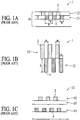
- Metrology targets often include two or more sets of lines of the type shown in FIGs. 1A-1B organized in cells. Different cells may have lines that run in different, e.g., mutually perpendicular directions.
- a metrology target may have a layer of material formed over one or more of the sets of lines.
- a layer of material may or may not exhibit residual topography.
- residual topography refers to parameters determined from topography observable in a layer overlying a structure that is due to the structure that underlies the layer.
- FIG. 1C illustrates a target 1C in which a layer of material 13 is formed over a set of lines 4. The layer is planarized and covered with a subsequent layer 15. If either or both layers 13, 15 are opaque, the underlying structure of the lines 4 is not observable.
- FIG. 1C illustrates a target 1C in which a layer of material 13 is formed over a set of lines 4. The layer is planarized and covered with a subsequent layer 15. If either or both layers 13, 15 are opaque, the underlying structure of the lines 4 is not observable.
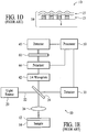
- FIG. IE An example of an apparatus 10 that may be used for scatterometry overlay metrology with a target of the type shown in FIGs. 1A-1B is shown in FIG. IE. A full description of this apparatus may be found in US Patent number 6,995,842 .
- the apparatus 10 may be designed to evaluate characteristics at the surface of a sample 14, such as thin film layers 12 and/or structural features such as critical dimensions.
- incident power detector 30 is provided to monitor fluctuations in the output power of the probe beam light source. As discussed in U.S. Pat. No. 5,181,080 , the incident power detector may be modified to minimize measurement errors which arise due to asymmetries of the beam.
- Light reflected from the target 1 formed on one or more layers of the sample 14 passes up through splitter 24 towards a photodetector 40.
- An output of the detector 40 may be supplied to a processor 50 for evaluation.
- the detector 40 may be configured to generate independent signals from regions along two pairs of mutually orthogonal axes.
- this goal may be achieved by using a photodetector having a plurality of spaced-apart light sensitive elements, e.g., photodiodes, photoresistors, or photovoltaic devices, each of which produces a distinct signal in response to radiation incident upon it.
- the light-sensitive elements may be configured in the form of a circle divided into multiple (e.g., eight) wedge shaped segments.
- the probe beam 22 is preferably centered on the detector 40 so that each segment intercepts an equal portion of the probe beam. It may also be desirable that the probe beam should underfill the detector 40.
- the optical characteristics 110 of the target 1 may then be used as an input to a metrology simulator 112, which computationally simulates operation of a metrology tool (e.g., metrology tool 10 ) that uses the target 1.
- a metrology simulator 112 may compute an estimated signal measured by the detector 40 based on input assumptions including the optical characteristics 110 of the target 1 and the metrology recipe used to measure the target.
- the metrology recipe may include parameters relevant to the process used to extract a metrology measurement made with the target 1 using the tool 10 from the optical characteristics 110.
- the metrology simulator 112 may analyze an angular or wavelength spectrum generated by the optical simulator and determine the angles or wavelengths corresponding to regions of maximum sensitivity to overlay in the spectrum and the relative intensity of those peaks. The results of the simulation may then be reviewed to determine domains in metrology characteristic space, e.g., in wavelength and angular (azimuthal and/or elevation) space, where the signal has a strong sensitivity to overlay.
- the metrology recipe may then be modified to weight wavelengths and/or angles within those domains more heavily. By weighting the metrology recipe towards wavelengths and/or angles for which the signal is particularly sensitive to overlay, the recipe may be optimized for high precision and sensitivity.
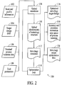
- One possible method 200 for implementing metrology target design in accordance with an embodiment of the present invention is illustrated in the flow diagram shown in FIG. 3 .
- This method may be implemented by computer software.
- Computer readable instructions for implementing the method 200 may be embodied in a computer readable medium, such as a computer memory, e.g., RAM, SRAM, DRAM, or ROM, or in a data storage medium, e.g., a disk, tape, CD-ROM and the like.
- Data for optical and metrology simulation may be input by a user or may be loaded from one or more data storage devices. This data may include optical characteristics of the metrology system 202, target design degrees of freedom 204, stack and profile information 206 and nominal process variation ranges 208.
- the optical characteristics and (optionally) the signal sensitivity may be applied to a metrology algorithm as indicated at 216.
- the metrology algorithm then outputs an estimated accuracy and precision prediction for specific metrology target/tool/stack combination as indicated at 218.
- the metrology algorithm may predict an offset determined from the wavelength or angular reflection spectrum.
- the accuracy of the offset prediction may be determined by comparing the predicted offset to an input value in the in the target design information.
- the precision of this prediction may be compared by determining the variation in the predicted offset over the process variation range.
- the instructions may, when executed may cause the processor unit 441 to a) receive input including information relating to a metrology target design, a substrate on which the target is to be formed, and a metrology system that will be used to measure the metrology target; b) model acquisition of a metrology signal with the metrology system using the metrology target information to generate one or more characteristics of the metrology target; c) apply a metrology algorithm to the characteristics of the metrology target to determine a predicted accuracy and precision of measurements made with the metrology system using the metrology target on the substrate; d) modify at least a portion of the information relating to the metrology target design and repeat b) and c) to optimize the target; and c) display or store information representing the optimized metrology target design.
- the optimized target design 447 may be formatted according to a suitable format for storage and/or display, such as GDSII.
- the controller 440 may also include well-known support circuits 450, such as input/output (I/O) circuits 451, power supplies (P/S) 452, a clock (CLK) 453 and cache 454.
- the controller 440 may also optionally include a user interface unit 448 and display unit 449 to facilitate interaction between the controller 440 and a user.
- the display unit 449 may be in the form of a cathode ray tube (CRT) or flat panel screen that displays text, numerals, or graphical symbols.
- the user interface 448 may include a keyboard, mouse, joystick, light pen or other device.
- the preceding components may exchange signals with each other via an internal bus 460.
- the controller 440 may be a general purpose computer that becomes a special purpose computer when running code that implements embodiments of the present invention as described herein.
Landscapes
- Physics & Mathematics (AREA)
- General Physics & Mathematics (AREA)
- Engineering & Computer Science (AREA)
- Computer Hardware Design (AREA)
- Theoretical Computer Science (AREA)
- General Engineering & Computer Science (AREA)
- Geometry (AREA)
- Evolutionary Computation (AREA)
- Length Measuring Devices By Optical Means (AREA)
- Exposure Of Semiconductors, Excluding Electron Or Ion Beam Exposure (AREA)
- Exposure And Positioning Against Photoresist Photosensitive Materials (AREA)
- Investigating Materials By The Use Of Optical Means Adapted For Particular Applications (AREA)
- Preparing Plates And Mask In Photomechanical Process (AREA)
Applications Claiming Priority (2)
| Application Number | Priority Date | Filing Date | Title |
|---|---|---|---|
| US12/350,826 US8214771B2 (en) | 2009-01-08 | 2009-01-08 | Scatterometry metrology target design optimization |
| PCT/US2010/020046 WO2010080732A2 (en) | 2009-01-08 | 2010-01-04 | Scatterometry metrology target design optimization |
Publications (3)
| Publication Number | Publication Date |
|---|---|
| EP2386114A2 EP2386114A2 (en) | 2011-11-16 |
| EP2386114A4 EP2386114A4 (en) | 2017-10-25 |
| EP2386114B1 true EP2386114B1 (en) | 2018-10-31 |
Family
ID=42312538
Family Applications (1)
| Application Number | Title | Priority Date | Filing Date |
|---|---|---|---|
| EP10729404.3A Active EP2386114B1 (en) | 2009-01-08 | 2010-01-04 | Scatterometry metrology target design optimization |
Country Status (5)
| Country | Link |
|---|---|
| US (1) | US8214771B2 (https=) |
| EP (1) | EP2386114B1 (https=) |
| JP (3) | JP5635011B2 (https=) |
| KR (1) | KR101281301B1 (https=) |
| WO (1) | WO2010080732A2 (https=) |
Families Citing this family (48)
| Publication number | Priority date | Publication date | Assignee | Title |
|---|---|---|---|---|
| US8214771B2 (en) * | 2009-01-08 | 2012-07-03 | Kla-Tencor Corporation | Scatterometry metrology target design optimization |
| US20130110477A1 (en) * | 2011-10-31 | 2013-05-02 | Stilian Pandev | Process variation-based model optimization for metrology |
| US9311431B2 (en) * | 2011-11-03 | 2016-04-12 | Kla-Tencor Corporation | Secondary target design for optical measurements |
| US20130297061A1 (en) * | 2012-05-03 | 2013-11-07 | National Taiwan University | Method and computer-aided design system of manufacturing an optical system |
| US9329033B2 (en) * | 2012-09-05 | 2016-05-03 | Kla-Tencor Corporation | Method for estimating and correcting misregistration target inaccuracy |
| US9879977B2 (en) * | 2012-11-09 | 2018-01-30 | Kla-Tencor Corporation | Apparatus and method for optical metrology with optimized system parameters |
| US20140136164A1 (en) * | 2012-11-09 | 2014-05-15 | Kla -Tencor Corporation | Analytic continuations to the continuum limit in numerical simulations of wafer response |
| US10769320B2 (en) * | 2012-12-18 | 2020-09-08 | Kla-Tencor Corporation | Integrated use of model-based metrology and a process model |
| WO2014138057A1 (en) | 2013-03-04 | 2014-09-12 | Kla-Tencor Corporation | Metrology target identification, design and verification |
| WO2014139855A1 (en) | 2013-03-14 | 2014-09-18 | Asml Netherlands B.V. | Patterning device, method of producing a marker on a substrate and device manufacturing method |
| US10955359B2 (en) * | 2013-11-12 | 2021-03-23 | International Business Machines Corporation | Method for quantification of process non uniformity using model-based metrology |
| CN105830069B (zh) * | 2013-12-11 | 2021-04-20 | 科磊股份有限公司 | 依据要求的目标及工艺灵敏度分析 |
| KR101860038B1 (ko) | 2013-12-30 | 2018-05-21 | 에이에스엠엘 네델란즈 비.브이. | 메트롤로지 타겟의 디자인을 위한 방법 및 장치 |
| JP6291581B2 (ja) * | 2013-12-30 | 2018-03-14 | エーエスエムエル ネザーランズ ビー.ブイ. | メトロロジーターゲットの設計のための方法及び装置 |
| US9553033B2 (en) * | 2014-01-15 | 2017-01-24 | Kla-Tencor Corporation | Semiconductor device models including re-usable sub-structures |
| WO2015124397A1 (en) | 2014-02-21 | 2015-08-27 | Asml Netherlands B.V. | Optimization of target arrangement and associated target |
| KR101906289B1 (ko) * | 2014-02-21 | 2018-10-10 | 에이에스엠엘 네델란즈 비.브이. | 리소그래피를 수반하는 제조 공정을 위한 공정 파라미터의 측정 |
| SG11201609566VA (en) * | 2014-06-02 | 2016-12-29 | Asml Netherlands Bv | Method of designing metrology targets, substrates having metrology targets, method of measuring overlay, and device manufacturing method |
| JP6421237B2 (ja) * | 2014-08-29 | 2018-11-07 | エーエスエムエル ネザーランズ ビー.ブイ. | メトロロジー方法、ターゲット、及び基板 |
| CN112331576B (zh) | 2014-10-03 | 2024-07-26 | 科磊股份有限公司 | 计量目标设计方法以及验证计量目标 |
| US9589079B2 (en) * | 2014-11-17 | 2017-03-07 | Sunedison, Inc. | Methods and systems for designing photovoltaic systems |
| US10185303B2 (en) | 2015-02-21 | 2019-01-22 | Kla-Tencor Corporation | Optimizing computational efficiency by multiple truncation of spatial harmonics |
| US11580274B2 (en) * | 2015-04-10 | 2023-02-14 | Asml Netherlands B.V. | Method and apparatus for inspection and metrology |
| WO2016172122A1 (en) * | 2015-04-21 | 2016-10-27 | Kla-Tencor Corporation | Metrology target design for tilted device designs |
| US9995689B2 (en) * | 2015-05-22 | 2018-06-12 | Nanometrics Incorporated | Optical metrology using differential fitting |
| US10754260B2 (en) | 2015-06-18 | 2020-08-25 | Kla-Tencor Corporation | Method and system for process control with flexible sampling |
| US9824176B2 (en) * | 2015-07-24 | 2017-11-21 | Nanometrics Incorporated | Optical critical dimension target design |
| WO2017032534A2 (en) * | 2015-08-27 | 2017-03-02 | Asml Netherlands B.V. | Lithographic apparatus and device manufacturing method |
| US10386829B2 (en) | 2015-09-18 | 2019-08-20 | Kla-Tencor Corporation | Systems and methods for controlling an etch process |
| US9697310B2 (en) * | 2015-11-02 | 2017-07-04 | Winbond Electronics Corporation | Level faults interception in integrated circuits |
| KR102513021B1 (ko) * | 2016-05-12 | 2023-03-21 | 에이에스엠엘 네델란즈 비.브이. | 측정치 획득 방법, 프로세스 단계 수행 장치, 계측 장치, 디바이스 제조 방법 |
| US10018919B2 (en) | 2016-05-29 | 2018-07-10 | Kla-Tencor Corporation | System and method for fabricating metrology targets oriented with an angle rotated with respect to device features |
| WO2017207269A1 (en) * | 2016-06-03 | 2017-12-07 | Asml Holding N.V. | Alignment system wafer stack beam analyzer |
| US10095122B1 (en) | 2016-06-30 | 2018-10-09 | Kla-Tencor Corporation | Systems and methods for fabricating metrology targets with sub-resolution features |
| US10527952B2 (en) * | 2016-10-25 | 2020-01-07 | Kla-Tencor Corporation | Fault discrimination and calibration of scatterometry overlay targets |
| US10496781B2 (en) | 2016-12-19 | 2019-12-03 | Kla Tencor Corporation | Metrology recipe generation using predicted metrology images |
| CN110249268B (zh) | 2017-02-02 | 2021-08-24 | Asml荷兰有限公司 | 量测方法和设备以及关联的计算机产品 |
| EP3367166A1 (en) * | 2017-02-24 | 2018-08-29 | ASML Netherlands B.V. | Method of measuring variation, inspection system, computer program, and computer system |
| WO2018197144A1 (en) | 2017-04-28 | 2018-11-01 | Asml Netherlands B.V. | Optimizing a sequence of processes for manufacturing of product units |
| US11112369B2 (en) * | 2017-06-19 | 2021-09-07 | Kla-Tencor Corporation | Hybrid overlay target design for imaging-based overlay and scatterometry-based overlay |
| JP7431824B2 (ja) * | 2018-11-21 | 2024-02-15 | ケーエルエー コーポレイション | スキャトロメトリオーバーレイ(scol)測定方法及びscol測定システム |
| WO2020122996A1 (en) * | 2018-12-12 | 2020-06-18 | Kla Corporation | Multiple-tool parameter set configuration and misregistration measurement system and method |
| WO2020190318A1 (en) * | 2019-03-21 | 2020-09-24 | Kla Corporation | Parameter-stable misregistration measurement amelioration in semiconductor devices |
| WO2021006890A1 (en) * | 2019-07-10 | 2021-01-14 | Kla-Tencor Corporation | Data-driven misregistration parameter configuration and measurement system and method |
| US12585201B2 (en) * | 2019-10-14 | 2026-03-24 | Asml Holding N.V. | Metrology mark structure and method of determining metrology mark structure |
| US11487929B2 (en) | 2020-04-28 | 2022-11-01 | Kla Corporation | Target design process for overlay targets intended for multi-signal measurements |
| KR20240037469A (ko) * | 2022-09-15 | 2024-03-22 | 에스케이하이닉스 주식회사 | 반도체 소자 제조 파라미터 설정 방법 및 장치 |
| KR102738956B1 (ko) * | 2023-10-31 | 2024-12-06 | (주)오로스 테크놀로지 | 오버레이 계측 방법 및 오버레이 계측 시스템 |
Family Cites Families (39)
| Publication number | Priority date | Publication date | Assignee | Title |
|---|---|---|---|---|
| US5166752A (en) | 1990-01-11 | 1992-11-24 | Rudolph Research Corporation | Simultaneous multiple angle/multiple wavelength ellipsometer and method |
| US5181080A (en) | 1991-12-23 | 1993-01-19 | Therma-Wave, Inc. | Method and apparatus for evaluating the thickness of thin films |
| JPH08202020A (ja) | 1995-01-31 | 1996-08-09 | Sony Corp | フォトマスクにおけるパターン形状評価方法、フォトマスク、フォトマスクの作製方法、フォトマスクのパターン形成方法、並びに露光方法 |
| US5805290A (en) | 1996-05-02 | 1998-09-08 | International Business Machines Corporation | Method of optical metrology of unresolved pattern arrays |
| JP2000021767A (ja) * | 1998-07-03 | 2000-01-21 | Canon Inc | 位置観察方法及び位置観察装置 |
| US6248602B1 (en) | 1999-11-01 | 2001-06-19 | Amd, Inc. | Method and apparatus for automated rework within run-to-run control semiconductor manufacturing |
| JP4077141B2 (ja) | 2000-06-30 | 2008-04-16 | 株式会社東芝 | デザインルール作成方法、デザインルール作成システム及び記録媒体 |
| US6430737B1 (en) | 2000-07-10 | 2002-08-06 | Mentor Graphics Corp. | Convergence technique for model-based optical and process correction |
| JP3347130B2 (ja) * | 2000-09-27 | 2002-11-20 | 株式会社東芝 | アライメント方法 |
| US6581193B1 (en) | 2001-06-13 | 2003-06-17 | Kla-Tencor | Apparatus and methods for modeling process effects and imaging effects in scanning electron microscopy |
| US6678046B2 (en) | 2001-08-28 | 2004-01-13 | Therma-Wave, Inc. | Detector configurations for optical metrology |
| US6673638B1 (en) | 2001-11-14 | 2004-01-06 | Kla-Tencor Corporation | Method and apparatus for the production of process sensitive lithographic features |
| US6886153B1 (en) | 2001-12-21 | 2005-04-26 | Kla-Tencor Corporation | Design driven inspection or measurement for semiconductor using recipe |
| FI113876B (fi) * | 2002-02-15 | 2004-06-30 | Valtion Teknillinen | Uudet tärkkelyspohjaiset liimat |
| US20030160163A1 (en) | 2002-02-25 | 2003-08-28 | Alan Wong | Optical metrology target design for simultaneous measurement of multiple periodic structures |
| US7712056B2 (en) * | 2002-06-07 | 2010-05-04 | Cadence Design Systems, Inc. | Characterization and verification for integrated circuit designs |
| US7092110B2 (en) | 2002-07-25 | 2006-08-15 | Timbre Technologies, Inc. | Optimized model and parameter selection for optical metrology |
| JP4080813B2 (ja) * | 2002-08-09 | 2008-04-23 | 株式会社東芝 | マーク設計システム、マーク設計方法、マーク設計プログラムおよびこのマーク設計方法を用いた半導体装置の製造方法 |
| US7266480B2 (en) * | 2002-10-01 | 2007-09-04 | The Regents Of The University Of California | Rapid scattering simulation of objects in imaging using edge domain decomposition |
| US20040181768A1 (en) | 2003-03-12 | 2004-09-16 | Krukar Richard H. | Model pattern simulation of semiconductor wafer processing steps |
| US7346878B1 (en) * | 2003-07-02 | 2008-03-18 | Kla-Tencor Technologies Corporation | Apparatus and methods for providing in-chip microtargets for metrology or inspection |
| US7608468B1 (en) * | 2003-07-02 | 2009-10-27 | Kla-Tencor Technologies, Corp. | Apparatus and methods for determining overlay and uses of same |
| US7135344B2 (en) | 2003-07-11 | 2006-11-14 | Applied Materials, Israel, Ltd. | Design-based monitoring |
| US8073667B2 (en) * | 2003-09-30 | 2011-12-06 | Tokyo Electron Limited | System and method for using first-principles simulation to control a semiconductor manufacturing process |
| US7573574B2 (en) | 2004-07-13 | 2009-08-11 | Asml Netherlands Bv | Lithographic apparatus and device manufacturing method |
| US7678516B2 (en) | 2004-07-22 | 2010-03-16 | Kla-Tencor Technologies Corp. | Test structures and methods for monitoring or controlling a semiconductor fabrication process |
| JP4904034B2 (ja) | 2004-09-14 | 2012-03-28 | ケーエルエー−テンカー コーポレイション | レチクル・レイアウト・データを評価するための方法、システム及び搬送媒体 |
| JP4856865B2 (ja) * | 2004-10-05 | 2012-01-18 | キヤノン株式会社 | 位置検出方法 |
| US7094507B2 (en) | 2004-10-29 | 2006-08-22 | Infineon Technologies Ag | Method for determining an optimal absorber stack geometry of a lithographic reflection mask |
| JP4707374B2 (ja) | 2004-11-26 | 2011-06-22 | Okiセミコンダクタ株式会社 | Esd保護回路の構成を決定する方法及びシミュレーション方法 |
| US20060117293A1 (en) * | 2004-11-30 | 2006-06-01 | Nigel Smith | Method for designing an overlay mark |
| TWI269870B (en) * | 2004-12-30 | 2007-01-01 | Ind Tech Res Inst | Method for deciding structure parameters of a grating |
| US7557921B1 (en) * | 2005-01-14 | 2009-07-07 | Kla-Tencor Technologies Corporation | Apparatus and methods for optically monitoring the fidelity of patterns produced by photolitographic tools |
| KR100660861B1 (ko) | 2005-02-23 | 2006-12-26 | 삼성전자주식회사 | 반도체 공정 결과를 예측하고 제어하는 반도체 공정 제어장치 |
| US7695876B2 (en) | 2005-08-31 | 2010-04-13 | Brion Technologies, Inc. | Method for identifying and using process window signature patterns for lithography process control |
| US7480050B2 (en) | 2006-02-09 | 2009-01-20 | Asml Netherlands B.V. | Lithographic system, sensor, and method of measuring properties of a substrate |
| US7925486B2 (en) * | 2006-03-14 | 2011-04-12 | Kla-Tencor Technologies Corp. | Computer-implemented methods, carrier media, and systems for creating a metrology target structure design for a reticle layout |
| US7528941B2 (en) * | 2006-06-01 | 2009-05-05 | Kla-Tencor Technolgies Corporation | Order selected overlay metrology |
| US8214771B2 (en) * | 2009-01-08 | 2012-07-03 | Kla-Tencor Corporation | Scatterometry metrology target design optimization |
-
2009
- 2009-01-08 US US12/350,826 patent/US8214771B2/en active Active
-
2010
- 2010-01-04 EP EP10729404.3A patent/EP2386114B1/en active Active
- 2010-01-04 WO PCT/US2010/020046 patent/WO2010080732A2/en not_active Ceased
- 2010-01-04 JP JP2011545386A patent/JP5635011B2/ja active Active
- 2010-01-04 KR KR1020117013856A patent/KR101281301B1/ko active Active
-
2014
- 2014-10-15 JP JP2014210497A patent/JP5855728B2/ja active Active
-
2015
- 2015-12-09 JP JP2015240051A patent/JP2016066093A/ja active Pending
Non-Patent Citations (1)
| Title |
|---|
| None * |
Also Published As
| Publication number | Publication date |
|---|---|
| WO2010080732A3 (en) | 2010-10-07 |
| KR101281301B1 (ko) | 2013-07-03 |
| JP5635011B2 (ja) | 2014-12-03 |
| WO2010080732A2 (en) | 2010-07-15 |
| JP2016066093A (ja) | 2016-04-28 |
| US20100175033A1 (en) | 2010-07-08 |
| EP2386114A2 (en) | 2011-11-16 |
| JP2015039021A (ja) | 2015-02-26 |
| KR20110095363A (ko) | 2011-08-24 |
| EP2386114A4 (en) | 2017-10-25 |
| JP2012514871A (ja) | 2012-06-28 |
| JP5855728B2 (ja) | 2016-02-09 |
| US8214771B2 (en) | 2012-07-03 |
Similar Documents
| Publication | Publication Date | Title |
|---|---|---|
| EP2386114B1 (en) | Scatterometry metrology target design optimization | |
| US20200218166A1 (en) | Metrology recipe selection | |
| TWI631431B (zh) | 度量衡方法、電腦產品及系統 | |
| KR102729959B1 (ko) | 기울어진 디바이스 설계를 위한 계측 타겟 설계 | |
| CN107741207B (zh) | 多重图案化参数的测量 | |
| JP6697560B2 (ja) | メトロロジ方法及び装置 | |
| TWI685720B (zh) | 用於微影設備的度量衡方法 | |
| US9091942B2 (en) | Scatterometry measurement of line edge roughness in the bright field | |
| KR20180005200A (ko) | 모델 기반의 핫 스팟 모니터링 | |
| JP7110327B2 (ja) | メトロロジ方法及び装置 | |
| KR102770686B1 (ko) | 다중-신호 측정을 위해 의도된 오버레이 타겟을 위한 타겟 설계 프로세스 | |
| US12210293B2 (en) | Method for determining a measurement recipe and associated apparatuses | |
| Levi et al. | A holistic metrology sensitivity study for pattern roughness quantification on EUV patterned device structures with mask design induced roughness | |
| Quintanilha et al. | Application of spectroscopic scatterometry method in hole matrices analysis | |
| TWI711890B (zh) | 在度量衡中的資料之估計 | |
| Lozenko et al. | Matching Between Simulations and Measurements As a Key Driver for Reliable Overlay Target Design Comparing overlay target simulations and actual measurements identifies inaccuracies in models and can help designers improve models. November 15th, 2018-By: GlobalFoundries |
Legal Events
| Date | Code | Title | Description |
|---|---|---|---|
| PUAI | Public reference made under article 153(3) epc to a published international application that has entered the european phase |
Free format text: ORIGINAL CODE: 0009012 |
|
| 17P | Request for examination filed |
Effective date: 20110808 |
|
| AK | Designated contracting states |
Kind code of ref document: A2 Designated state(s): AT BE BG CH CY CZ DE DK EE ES FI FR GB GR HR HU IE IS IT LI LT LU LV MC MK MT NL NO PL PT RO SE SI SK SM TR |
|
| DAX | Request for extension of the european patent (deleted) | ||
| REG | Reference to a national code |
Ref country code: DE Ref legal event code: R079 Ref document number: 602010054750 Country of ref document: DE Free format text: PREVIOUS MAIN CLASS: H01L0021660000 Ipc: G03F0007200000 |
|
| A4 | Supplementary search report drawn up and despatched |
Effective date: 20170921 |
|
| RIC1 | Information provided on ipc code assigned before grant |
Ipc: H01L 21/66 20060101ALI20170915BHEP Ipc: G03F 7/20 20060101AFI20170915BHEP |
|
| GRAP | Despatch of communication of intention to grant a patent |
Free format text: ORIGINAL CODE: EPIDOSNIGR1 |
|
| STAA | Information on the status of an ep patent application or granted ep patent |
Free format text: STATUS: GRANT OF PATENT IS INTENDED |
|
| INTG | Intention to grant announced |
Effective date: 20180614 |
|
| GRAS | Grant fee paid |
Free format text: ORIGINAL CODE: EPIDOSNIGR3 |
|
| GRAA | (expected) grant |
Free format text: ORIGINAL CODE: 0009210 |
|
| STAA | Information on the status of an ep patent application or granted ep patent |
Free format text: STATUS: THE PATENT HAS BEEN GRANTED |
|
| AK | Designated contracting states |
Kind code of ref document: B1 Designated state(s): AT BE BG CH CY CZ DE DK EE ES FI FR GB GR HR HU IE IS IT LI LT LU LV MC MK MT NL NO PL PT RO SE SI SK SM TR |
|
| REG | Reference to a national code |
Ref country code: CH Ref legal event code: EP Ref country code: GB Ref legal event code: FG4D |
|
| REG | Reference to a national code |
Ref country code: AT Ref legal event code: REF Ref document number: 1060113 Country of ref document: AT Kind code of ref document: T Effective date: 20181115 |
|
| REG | Reference to a national code |
Ref country code: DE Ref legal event code: R096 Ref document number: 602010054750 Country of ref document: DE |
|
| REG | Reference to a national code |
Ref country code: IE Ref legal event code: FG4D |
|
| REG | Reference to a national code |
Ref country code: NL Ref legal event code: FP |
|
| REG | Reference to a national code |
Ref country code: LT Ref legal event code: MG4D |
|
| REG | Reference to a national code |
Ref country code: AT Ref legal event code: MK05 Ref document number: 1060113 Country of ref document: AT Kind code of ref document: T Effective date: 20181031 |
|
| PG25 | Lapsed in a contracting state [announced via postgrant information from national office to epo] |
Ref country code: FI Free format text: LAPSE BECAUSE OF FAILURE TO SUBMIT A TRANSLATION OF THE DESCRIPTION OR TO PAY THE FEE WITHIN THE PRESCRIBED TIME-LIMIT Effective date: 20181031 Ref country code: LV Free format text: LAPSE BECAUSE OF FAILURE TO SUBMIT A TRANSLATION OF THE DESCRIPTION OR TO PAY THE FEE WITHIN THE PRESCRIBED TIME-LIMIT Effective date: 20181031 Ref country code: IS Free format text: LAPSE BECAUSE OF FAILURE TO SUBMIT A TRANSLATION OF THE DESCRIPTION OR TO PAY THE FEE WITHIN THE PRESCRIBED TIME-LIMIT Effective date: 20190228 Ref country code: HR Free format text: LAPSE BECAUSE OF FAILURE TO SUBMIT A TRANSLATION OF THE DESCRIPTION OR TO PAY THE FEE WITHIN THE PRESCRIBED TIME-LIMIT Effective date: 20181031 Ref country code: AT Free format text: LAPSE BECAUSE OF FAILURE TO SUBMIT A TRANSLATION OF THE DESCRIPTION OR TO PAY THE FEE WITHIN THE PRESCRIBED TIME-LIMIT Effective date: 20181031 Ref country code: PL Free format text: LAPSE BECAUSE OF FAILURE TO SUBMIT A TRANSLATION OF THE DESCRIPTION OR TO PAY THE FEE WITHIN THE PRESCRIBED TIME-LIMIT Effective date: 20181031 Ref country code: NO Free format text: LAPSE BECAUSE OF FAILURE TO SUBMIT A TRANSLATION OF THE DESCRIPTION OR TO PAY THE FEE WITHIN THE PRESCRIBED TIME-LIMIT Effective date: 20190131 Ref country code: BG Free format text: LAPSE BECAUSE OF FAILURE TO SUBMIT A TRANSLATION OF THE DESCRIPTION OR TO PAY THE FEE WITHIN THE PRESCRIBED TIME-LIMIT Effective date: 20190131 Ref country code: ES Free format text: LAPSE BECAUSE OF FAILURE TO SUBMIT A TRANSLATION OF THE DESCRIPTION OR TO PAY THE FEE WITHIN THE PRESCRIBED TIME-LIMIT Effective date: 20181031 Ref country code: LT Free format text: LAPSE BECAUSE OF FAILURE TO SUBMIT A TRANSLATION OF THE DESCRIPTION OR TO PAY THE FEE WITHIN THE PRESCRIBED TIME-LIMIT Effective date: 20181031 |
|
| PG25 | Lapsed in a contracting state [announced via postgrant information from national office to epo] |
Ref country code: PT Free format text: LAPSE BECAUSE OF FAILURE TO SUBMIT A TRANSLATION OF THE DESCRIPTION OR TO PAY THE FEE WITHIN THE PRESCRIBED TIME-LIMIT Effective date: 20190301 Ref country code: SE Free format text: LAPSE BECAUSE OF FAILURE TO SUBMIT A TRANSLATION OF THE DESCRIPTION OR TO PAY THE FEE WITHIN THE PRESCRIBED TIME-LIMIT Effective date: 20181031 Ref country code: GR Free format text: LAPSE BECAUSE OF FAILURE TO SUBMIT A TRANSLATION OF THE DESCRIPTION OR TO PAY THE FEE WITHIN THE PRESCRIBED TIME-LIMIT Effective date: 20190201 |
|
| PG25 | Lapsed in a contracting state [announced via postgrant information from national office to epo] |
Ref country code: CZ Free format text: LAPSE BECAUSE OF FAILURE TO SUBMIT A TRANSLATION OF THE DESCRIPTION OR TO PAY THE FEE WITHIN THE PRESCRIBED TIME-LIMIT Effective date: 20181031 Ref country code: DK Free format text: LAPSE BECAUSE OF FAILURE TO SUBMIT A TRANSLATION OF THE DESCRIPTION OR TO PAY THE FEE WITHIN THE PRESCRIBED TIME-LIMIT Effective date: 20181031 |
|
| REG | Reference to a national code |
Ref country code: DE Ref legal event code: R097 Ref document number: 602010054750 Country of ref document: DE |
|
| PG25 | Lapsed in a contracting state [announced via postgrant information from national office to epo] |
Ref country code: EE Free format text: LAPSE BECAUSE OF FAILURE TO SUBMIT A TRANSLATION OF THE DESCRIPTION OR TO PAY THE FEE WITHIN THE PRESCRIBED TIME-LIMIT Effective date: 20181031 Ref country code: MC Free format text: LAPSE BECAUSE OF FAILURE TO SUBMIT A TRANSLATION OF THE DESCRIPTION OR TO PAY THE FEE WITHIN THE PRESCRIBED TIME-LIMIT Effective date: 20181031 Ref country code: SM Free format text: LAPSE BECAUSE OF FAILURE TO SUBMIT A TRANSLATION OF THE DESCRIPTION OR TO PAY THE FEE WITHIN THE PRESCRIBED TIME-LIMIT Effective date: 20181031 Ref country code: RO Free format text: LAPSE BECAUSE OF FAILURE TO SUBMIT A TRANSLATION OF THE DESCRIPTION OR TO PAY THE FEE WITHIN THE PRESCRIBED TIME-LIMIT Effective date: 20181031 Ref country code: SK Free format text: LAPSE BECAUSE OF FAILURE TO SUBMIT A TRANSLATION OF THE DESCRIPTION OR TO PAY THE FEE WITHIN THE PRESCRIBED TIME-LIMIT Effective date: 20181031 |
|
| REG | Reference to a national code |
Ref country code: CH Ref legal event code: PL |
|
| PLBE | No opposition filed within time limit |
Free format text: ORIGINAL CODE: 0009261 |
|
| STAA | Information on the status of an ep patent application or granted ep patent |
Free format text: STATUS: NO OPPOSITION FILED WITHIN TIME LIMIT |
|
| PG25 | Lapsed in a contracting state [announced via postgrant information from national office to epo] |
Ref country code: LU Free format text: LAPSE BECAUSE OF NON-PAYMENT OF DUE FEES Effective date: 20190104 |
|
| 26N | No opposition filed |
Effective date: 20190801 |
|
| PG25 | Lapsed in a contracting state [announced via postgrant information from national office to epo] |
Ref country code: SI Free format text: LAPSE BECAUSE OF FAILURE TO SUBMIT A TRANSLATION OF THE DESCRIPTION OR TO PAY THE FEE WITHIN THE PRESCRIBED TIME-LIMIT Effective date: 20181031 |
|
| PG25 | Lapsed in a contracting state [announced via postgrant information from national office to epo] |
Ref country code: LI Free format text: LAPSE BECAUSE OF NON-PAYMENT OF DUE FEES Effective date: 20190131 Ref country code: CH Free format text: LAPSE BECAUSE OF NON-PAYMENT OF DUE FEES Effective date: 20190131 |
|
| PG25 | Lapsed in a contracting state [announced via postgrant information from national office to epo] |
Ref country code: TR Free format text: LAPSE BECAUSE OF FAILURE TO SUBMIT A TRANSLATION OF THE DESCRIPTION OR TO PAY THE FEE WITHIN THE PRESCRIBED TIME-LIMIT Effective date: 20181031 |
|
| PG25 | Lapsed in a contracting state [announced via postgrant information from national office to epo] |
Ref country code: MT Free format text: LAPSE BECAUSE OF NON-PAYMENT OF DUE FEES Effective date: 20190104 |
|
| PG25 | Lapsed in a contracting state [announced via postgrant information from national office to epo] |
Ref country code: CY Free format text: LAPSE BECAUSE OF FAILURE TO SUBMIT A TRANSLATION OF THE DESCRIPTION OR TO PAY THE FEE WITHIN THE PRESCRIBED TIME-LIMIT Effective date: 20181031 |
|
| PG25 | Lapsed in a contracting state [announced via postgrant information from national office to epo] |
Ref country code: HU Free format text: LAPSE BECAUSE OF FAILURE TO SUBMIT A TRANSLATION OF THE DESCRIPTION OR TO PAY THE FEE WITHIN THE PRESCRIBED TIME-LIMIT; INVALID AB INITIO Effective date: 20100104 |
|
| PG25 | Lapsed in a contracting state [announced via postgrant information from national office to epo] |
Ref country code: MK Free format text: LAPSE BECAUSE OF FAILURE TO SUBMIT A TRANSLATION OF THE DESCRIPTION OR TO PAY THE FEE WITHIN THE PRESCRIBED TIME-LIMIT Effective date: 20181031 |
|
| P01 | Opt-out of the competence of the unified patent court (upc) registered |
Effective date: 20230525 |
|
| PGFP | Annual fee paid to national office [announced via postgrant information from national office to epo] |
Ref country code: NL Payment date: 20250127 Year of fee payment: 16 |
|
| PGFP | Annual fee paid to national office [announced via postgrant information from national office to epo] |
Ref country code: DE Payment date: 20250129 Year of fee payment: 16 |
|
| PGFP | Annual fee paid to national office [announced via postgrant information from national office to epo] |
Ref country code: GB Payment date: 20260127 Year of fee payment: 17 |
|
| PGFP | Annual fee paid to national office [announced via postgrant information from national office to epo] |
Ref country code: IE Payment date: 20260127 Year of fee payment: 17 |
|
| PGFP | Annual fee paid to national office [announced via postgrant information from national office to epo] |
Ref country code: BE Payment date: 20260127 Year of fee payment: 17 Ref country code: IT Payment date: 20260121 Year of fee payment: 17 |
|
| PGFP | Annual fee paid to national office [announced via postgrant information from national office to epo] |
Ref country code: FR Payment date: 20260126 Year of fee payment: 17 |