EP2384841A2 - System zur Abgabe von Weichlot zum Montieren von Halbleiterchips unter Verwendung von mehreren Lötdrähten - Google Patents
System zur Abgabe von Weichlot zum Montieren von Halbleiterchips unter Verwendung von mehreren Lötdrähten Download PDFInfo
- Publication number
- EP2384841A2 EP2384841A2 EP11003586A EP11003586A EP2384841A2 EP 2384841 A2 EP2384841 A2 EP 2384841A2 EP 11003586 A EP11003586 A EP 11003586A EP 11003586 A EP11003586 A EP 11003586A EP 2384841 A2 EP2384841 A2 EP 2384841A2
- Authority
- EP
- European Patent Office
- Prior art keywords
- solder
- dispensing
- substrate
- dispensing body
- wire
- Prior art date
- Legal status (The legal status is an assumption and is not a legal conclusion. Google has not performed a legal analysis and makes no representation as to the accuracy of the status listed.)
- Withdrawn
Links
Images


Classifications
-
- B—PERFORMING OPERATIONS; TRANSPORTING
- B23—MACHINE TOOLS; METAL-WORKING NOT OTHERWISE PROVIDED FOR
- B23K—SOLDERING OR UNSOLDERING; WELDING; CLADDING OR PLATING BY SOLDERING OR WELDING; CUTTING BY APPLYING HEAT LOCALLY, e.g. FLAME CUTTING; WORKING BY LASER BEAM
- B23K1/00—Soldering, e.g. brazing, or unsoldering
- B23K1/20—Preliminary treatment of work or areas to be soldered, e.g. in respect of a galvanic coating
-
- B—PERFORMING OPERATIONS; TRANSPORTING
- B23—MACHINE TOOLS; METAL-WORKING NOT OTHERWISE PROVIDED FOR
- B23K—SOLDERING OR UNSOLDERING; WELDING; CLADDING OR PLATING BY SOLDERING OR WELDING; CUTTING BY APPLYING HEAT LOCALLY, e.g. FLAME CUTTING; WORKING BY LASER BEAM
- B23K1/00—Soldering, e.g. brazing, or unsoldering
- B23K1/0008—Soldering, e.g. brazing, or unsoldering specially adapted for particular articles or work
- B23K1/0016—Brazing of electronic components
-
- B—PERFORMING OPERATIONS; TRANSPORTING
- B23—MACHINE TOOLS; METAL-WORKING NOT OTHERWISE PROVIDED FOR
- B23K—SOLDERING OR UNSOLDERING; WELDING; CLADDING OR PLATING BY SOLDERING OR WELDING; CUTTING BY APPLYING HEAT LOCALLY, e.g. FLAME CUTTING; WORKING BY LASER BEAM
- B23K3/00—Tools, devices, or special appurtenances for soldering, e.g. brazing, or unsoldering, not specially adapted for particular methods
- B23K3/06—Solder feeding devices; Solder melting pans
- B23K3/0607—Solder feeding devices
- B23K3/063—Solder feeding devices for wire feeding
-
- B—PERFORMING OPERATIONS; TRANSPORTING
- B23—MACHINE TOOLS; METAL-WORKING NOT OTHERWISE PROVIDED FOR
- B23K—SOLDERING OR UNSOLDERING; WELDING; CLADDING OR PLATING BY SOLDERING OR WELDING; CUTTING BY APPLYING HEAT LOCALLY, e.g. FLAME CUTTING; WORKING BY LASER BEAM
- B23K2101/00—Articles made by soldering, welding or cutting
- B23K2101/36—Electric or electronic devices
- B23K2101/40—Semiconductor devices
-
- H10W72/0113—
Definitions
- the present invention relates generally to the fabrication and packaging of integrated circuit components, and in particular, to the attachment of semiconductor chips to substrates by the use of solders.
- Semiconductor chips may be bonded onto metallic substrates such as lead frames by soldering.
- power semiconductors are commonly fixed to lead frames by using soft solder.
- Power devices are widely used in the automotive industry due to their high thermal and electrical performance, and soft solder is generally chosen as the chip attach layer for such semiconductor packages.
- the soldered joint not only provides mechanical fixation of the chip, but it also ensures that heat which is produced in the semiconductor chip during operation is dissipated more efficiently than a joint comprising a non-conductive adhesive. Additionally, the soft solder provides a good electrical path for the semiconductor chips.
- soldered joint having a stipulated thickness is required.
- the layer of solder should wet the entire area of the semiconductor chip evenly. Furthermore, it should be completely free from air cavities and contamination by impurities. The solder should not protrude from the edges nor spread beyond the surface area of the bond pad, in what is known as bleeding. To achieve this, the stipulated amount of solder should be dispensed and accurately positioned onto the substrate before bonding the semiconductor chip.
- soft soldering of a semiconductor chip to a lead frame entails dispensing an amount of solder onto the lead frame before positioning the chip. This may involve touching one end of a solder wire at the position of the lead frame where the chip is to be located.
- the lead frame is preheated to a temperature which is above the melting point of the solder so that the solder wire melts upon contact with the lead frame.
- a prescribed length of the wire is fed to the lead frame and it is continuously or intermittently melted onto the lead frame.
- the solder wire which does not melt is then pulled back leaving a droplet of solder on the lead frame.
- the solder droplet remains molten when the lead frame is maintained at a temperature above the melting point of the solder.
- a conventional method to modify the shape of a solder droplet utilizes spankers.
- the substrate carrying a solder droplet is transferred to a spanking zone where a spanker in the form of a rectangular mold is located.
- the rectangular mold moves downwards to contact the solder droplet and to spread it inside the spanker mold cavity to form a rectangular footprint.
- a spanker typically comprises a shaft which can be lifted or lowered with respect to the substrate, and a stamp or punch connected to it wherein the stamping or punching surface faces the substrate.
- Deviations in thickness and position of the substrate as well as possible slanting of the substrate may adversely affect the thickness and lateral distribution of the solder. Even slight deviations in the angle between the punch surface and the surface of the substrate may lead to considerable lateral displacement of solder droplets.
- flattening the solder droplets by means of the spanking stamp or punch results in solder spots which may be more or less rounded at their edges and which do not conform exactly to the rectangular or square shape of the chips.
- an apparatus for dispensing solder onto a substrate for mounting a semiconductor chip on the substrate comprising: a dispensing body; and first and second dispensing channels extending through the dispensing body, each dispensing channel being operative to receive a separate solder wire to feed the solder wire to an end of the dispensing body facing the substrate; wherein the dispensing channels are operative to introduce the solder wires in a solid state simultaneously from the end of the dispensing body to be melted upon contact with the substrate which is heated.
- a method for dispensing solder onto a substrate for mounting a semiconductor chip on the substrate comprising the steps of: providing a dispensing body; passing multiple solder wires through multiple dispensing channels extending through the dispensing body; feeding the solder wire to an end of the dispensing body facing the substrate; and introducing the multiple solder wires simultaneously from the end of the dispensing body in a solid state and melting the solder wires upon contact with the substrate which is heated.
- FIG. 1 is a side view of a solder dispenser 10 for dispensing soft solder according to the preferred embodiment of the invention.
- the solder dispenser 10 is positionable over a substrate 12 such as a lead frame or other device and a length of solder wire 24 is passed through the solder dispenser 10 for feeding the solder wire 24 to the substrate 12.
- a substrate 12 such as a lead frame or other device
- solder wire 24 is passed through the solder dispenser 10 for feeding the solder wire 24 to the substrate 12.
- two or more separate solder wires 24 are fed into and dispensed from the solder dispenser 10 simultaneously.
- the solder dispenser 10 comprises a wire feeder and a dispensing body 18.
- the wire feeder of the preferred embodiment may comprise a pair of press rollers 14 which engage each other so that the solder wires 24 are guided via feeding channels located on the press rollers 14 for controlled feeding of the solder wires 24 into the solder dispenser 10 and towards the substrate 12 in a feeding direction.
- the feeding channel has a V-shaped cavity enabling the feeding channel to guide and position a solder wire 24 through the press rollers 14.
- the feeding direction is in a vertical or Z direction.
- the solder wires 24 are guided through the press rollers 14 by wire spools 13. Since multiple solder wires 24 are fed into the solder dispenser 10, there are a corresponding number of wire spools 13 to guide the solder wires 24 through separate feeding channels on the press rollers 14 into the solder dispenser 10.
- a clamping force is exerted by the press rollers 14 on the solder wires 24, and the clamping force is controlled by varying the gap between the pair of pressed rollers 14 by adjusting a connecting spring or a screw (not shown).
- the volume of the solder wire 24 dispensed may be regulated accordingly.
- solder wires 24 that are dispensed from the solder dispenser 10 at an end of the dispensing body 18 facing a substrate 12 contact a target bond pad on the substrate 12 which is heated.
- the end of the solder wire 24 melts on a surface of the bond pad.
- the solder wires 24 form a molten solder dot or dots or a written liquid solder pattern according to a predetermined volume, position and shape.
- the volume and shape of the resultant solder footprint is determined by the design of the feeding channel and dispensing channels.
- the written liquid solder pattern is obtained from the controlled motion of the solder dispenser 10 in the X-Y horizontal directions.
- a solder wire guiding nut 16 guides the solder wire 24 through a centrally-located hole in the solder dispenser 10.
- a positioning device such as an X-Y table 17, is coupled to the solder dispenser 10 and configured for moving the solder dispenser 10 relative to the substrate 12 along at least one of two orthogonal axes that are substantially perpendicular to the wire feeding direction.
- the two orthogonal axes are the X and Y axes.
- the solder dispenser 10 is drivable in the X and Y directions by the X-Y table 17, and is able to dispense solder in any X-Y direction, such as diagonally onto the substrate 12, as the solder dispenser 10 moves.
- the X-Y table 17 may therefore move the solder dispenser 10 relative to the substrate 12 along at least one of the X and/or Y axes contemporaneously with the press rollers 14 feeding a solder wire 24 to the substrate 12 in the Z axis, whereby to dispense molten solder onto the substrate 12.
- the solder dispenser 10 has a solder wire cooling tube enclosing a cooling chamber located along the length of the dispensing body 18.
- the cooling chamber is connected to a cooling gas supply via a cooling gas inlet 20.
- the cooling gas leaves the cooling chamber through a cooling gas outlet 22, carrying with it the heat received from a heat tunnel on which the substrate 12 is placed.
- FIG. 2 is a longitudinal cross-sectional view of a tubular dispensing body 18 of the solder dispenser 10 of FIG. 1 .
- guide funnels 26 are located at the top of the solder dispenser 10 facing the feeding channels, and opposite to the end of the dispensing body 18 facing the substrate 12.
- Each guide funnel 26 guides a solder wire 24 which is fed from into a feeding channel.
- the guide funnels 26 are connected to first and second dispensing channels 19 extending through the dispensing body 18 and are located in a ceramic tube with a metal cover. Multiple dispensing channels 19 may receive and dispense multiple solder wires 24 simultaneously.
- the dispensing channels 19 and the guide funnels 26 are dielectric so as to electrically insulate the solder wire 24 in the solder dispenser 10. Together with the feeding channels which are also dielectric, the dispensing channels 19 and the guide funnels 26 allow each solder wire 24 to conduct contact searching of bond pad surface on the substrate 12 in order to dispense a sufficient amount of the solder wire 24 to form solder dots or to write a solder pattern onto the bond pad.
- solder dispenser 10 has a solder wire cooling tube enclosing a cooling chamber 28 located along the length of the dispensing body 18 for dissipating heat received from a heat tunnel in which the substrate 12 is placed.
- the cooling chamber 28 is connected to a cooling gas supply via a cooling gas inlet 20. Cooling gas such as compressed air is injected into the cooling chamber 28 through the cooling gas inlet 20 and leaves through a cooling gas outlet 22, thereby carrying away the heat received from the heat tunnel. This forms an air flow internally through the dispensing body 18.
- Cooling gas such as compressed air is injected into the cooling chamber 28 through the cooling gas inlet 20 and leaves through a cooling gas outlet 22, thereby carrying away the heat received from the heat tunnel. This forms an air flow internally through the dispensing body 18.
- the cooling gas cools the dispensing channel 19 before exiting the cooling chamber 28 at the gas outlet 22.
- the cooling chamber 28 is sealed near opposite ends of the dispensing body 18 using cooling gas sealants 30.
- the cooling process is important to maintain the solder dispenser 10 at a lower temperature to ensure that the solder wire 24 remains solid within the solder dispenser 10. By controlling the flow rate of the compressed air, the solder wires 24 are kept in solid form in the solder dispenser 10 until the wires contact the heated substrate.
- Contact search with respect to the surface of the substrate 12 is usefully carried out to sense contact between the dispenser tip 32 and the substrate 12 during setup prior to dispensing the solder wire 24.
- Such setup allows a contact level to be measured and the feeding distance to be established, which will assist in controlling the volume of the solder wire 24 dispensed.
- the contact sensor and/or additional contact sensors may also be electrically connected to the solder wires 24, and operative to sense contact between the solder wire 24 and the substrate 12 at a start of a solder dispensing operation. By sensing contact between the solder wire 24 and the substrate 12 at the start of dispensing, a dispensed solder wire length during the operation can be more precisely determined.
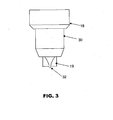
- FIG. 3 is an isometric view of a dispenser tip 32 of the solder dispenser 10 of FIG. 1 incorporating a contact sensor.
- the dispenser tip 32 comprises a metal tip which protrudes from the dispensing channels 19.
- the contact sensor of the dispenser tip 32 electrically monitors contact between the metallic dispenser tip 32 and the metallic substrate 12 during setup and in order to accurately establish a dispensing level or a gap between the dispenser tip 32 and a bond pad surface.
- the contact sensor is activated to locate a contact position at the level of the bond pad, before the dispensing body 18 moves upwards to a prescribed dispensing level spaced from the contact position at a predetermined distance over the bond pad or substrate 12.
- Solder wires 24 are then fed to the surface of the bond pad from the adjusted dispensing level.
- the contact sensor controls the volume of solder wire 24 that is dispensed onto the bond pad. Therefore, the preferred embodiment of this invention provides a method of dispensing solder wire 24 to form grid array dots or thin patterns on a bond pad with high productivity.
- the contact sensor of the dispenser tip 32 or other contact sensors may be electrically connected to the solder wires 24 such that a precise moment at which the solder wires 24 contact the bond pad or substrate 12 at the start of dispensing is determined. Thereafter, a volume of dispensed solder is equivalent to a length of solder wire 24 fed to the bond pad or substrate 12 from the start of dispensing.
- the solder dispenser 10 is first positioned by the X-Y table 17 over a targetted bond pad on the substrate 12.
- the dispenser tip 32 is configured to rest at a predetermined height from the surface of the bond pad by the contact sensor within the dispenser tip 32.
- the substrate 12 is heated in an enclosed heat tunnel in a forming gas environment to a predetermined temperature, which is usually about 30 to 80° C above the melting point of the solder material.
- solder wires 24 are driven through separate feeding channels by the pressed rollers 14.
- the solder wires 24 are guided into the dispensing channels 19 in the dispenser body 18.
- the temperature of the dispensing channels 19 is kept low by compressed air or other gases so that the solder wires 24 remain solid until the solder wires 24 contact the heated surface of the substrate 12.
- the rate of melting the solder wires 24 depends on the dispensing distance of the solder wires 24 from the heated substrate 12.
- solder wires 24 melt and form one or more liquid domes, dots or a written solder pattern depending on the manner of deposition.
- the solder wire 24 that is not melted and remains solid is withdrawn from the surface of the subtrate and this ends the dispensing and/or pattern-writing process on the substrate.
- solder dispenser 10 incorporating multiple dispensing channels 19 dispensing multiple solder wires 24 simultaneously in dots or multiple written patterns as described above is advantageous over solder dispensing via a single dispensing channel.
- the single dispensing channel 19 usually dispenses a single solder dot in the form of a dome which is rather thick and uneven, and may not allow a die to be attached properly. Multiple small dots of solder which may be in grid array format are more effective as a thinner dome of solder is formed allowing for more precise die attachment.
- Dispensing solder through multiple channels at the same time forms thinner and flatter solder patterns, that is, thin domes of solder material that are more uniformly spread out. This is preferred as compared to dispensing using a single solder wire as a void-free and a more even solder layer is obtained which helps to avoid tilted chips.
- solder wire dispensing speeds up the dispensing process to increase productivity of soldering and decreases the extent of oxidation of the solder. Furthermore, the incidence of solder wire jamming and formation of incomplete patterns which occur frequently in a single solder wire dispenser is avoided using the pattern solder dispensing method as described above.
Landscapes
- Engineering & Computer Science (AREA)
- Mechanical Engineering (AREA)
- Die Bonding (AREA)
- Electric Connection Of Electric Components To Printed Circuits (AREA)
Applications Claiming Priority (1)
| Application Number | Priority Date | Filing Date | Title |
|---|---|---|---|
| US12/773,099 US20110272452A1 (en) | 2010-05-04 | 2010-05-04 | System for dispensing soft solder for mounting semiconductor chips using multiple solder wires |
Publications (1)
| Publication Number | Publication Date |
|---|---|
| EP2384841A2 true EP2384841A2 (de) | 2011-11-09 |
Family
ID=44303298
Family Applications (1)
| Application Number | Title | Priority Date | Filing Date |
|---|---|---|---|
| EP11003586A Withdrawn EP2384841A2 (de) | 2010-05-04 | 2011-05-03 | System zur Abgabe von Weichlot zum Montieren von Halbleiterchips unter Verwendung von mehreren Lötdrähten |
Country Status (8)
| Country | Link |
|---|---|
| US (2) | US20110272452A1 (de) |
| EP (1) | EP2384841A2 (de) |
| JP (1) | JP2011238924A (de) |
| KR (1) | KR20110122636A (de) |
| CN (1) | CN102233465A (de) |
| PH (1) | PH12011000137A1 (de) |
| SG (1) | SG175543A1 (de) |
| TW (1) | TW201203410A (de) |
Cited By (1)
| Publication number | Priority date | Publication date | Assignee | Title |
|---|---|---|---|---|
| US9339885B2 (en) | 2012-07-05 | 2016-05-17 | Besi Switzerland Ag | Method and apparatus for dispensing flux-free solder on a substrate |
Families Citing this family (5)
| Publication number | Priority date | Publication date | Assignee | Title |
|---|---|---|---|---|
| US8987892B2 (en) | 2013-05-10 | 2015-03-24 | Raytheon Company | Method for creating a selective solder seal interface for an integrated circuit cooling system |
| JP6800768B2 (ja) * | 2017-02-01 | 2020-12-16 | 株式会社日立製作所 | 半田付け装置 |
| US10457148B2 (en) * | 2017-02-24 | 2019-10-29 | Epic Battery Inc. | Solar car |
| CN109093230B (zh) * | 2018-09-18 | 2024-01-30 | 昆山华恒焊接股份有限公司 | 用于棒状焊丝的自动送丝机构及自动焊接机 |
| DE112022003797T5 (de) * | 2021-08-04 | 2024-06-13 | Besi Switzerland Ag | Vorrichtung zum Abgeben eines Lotdrahts |
Family Cites Families (12)
| Publication number | Priority date | Publication date | Assignee | Title |
|---|---|---|---|---|
| DE2618796C2 (de) * | 1976-02-28 | 1986-09-11 | Telefunken electronic GmbH, 7100 Heilbronn | Anordnung zur Führung von Anschlußdrähten |
| US4555052A (en) * | 1983-02-28 | 1985-11-26 | Fairchild Camera & Instrument Corporation | Lead wire bond attempt detection |
| JPH036034A (ja) * | 1989-06-02 | 1991-01-11 | Nec Yamagata Ltd | ワイヤボンディング装置 |
| JPH0745646A (ja) * | 1993-07-28 | 1995-02-14 | Hitachi Ltd | はんだ塗布装置 |
| JP2569921Y2 (ja) * | 1993-12-20 | 1998-04-28 | 上田日本無線株式会社 | レーザビームを利用した半田付け装置 |
| JPH10296436A (ja) * | 1997-04-25 | 1998-11-10 | Matsushita Electric Ind Co Ltd | 糸はんだ送給装置 |
| JP2000012567A (ja) * | 1998-06-19 | 2000-01-14 | Sanyo Electric Co Ltd | ダイボンダの接合材供給方法およびその装置 |
| JP3623703B2 (ja) * | 1999-11-29 | 2005-02-23 | Nec液晶テクノロジー株式会社 | 電子部品半田付け装置 |
| SG91867A1 (en) * | 2000-05-24 | 2002-10-15 | Casem Asia Pte Ltd | Improved apparatus and method for dispensing solder |
| JP4080326B2 (ja) * | 2002-12-27 | 2008-04-23 | キヤノンマシナリー株式会社 | ろう材供給ノズル |
| US7735715B2 (en) * | 2007-12-07 | 2010-06-15 | Asm Assembly Automation Ltd | Dispensing solder for mounting semiconductor chips |
| US8581146B2 (en) * | 2008-10-22 | 2013-11-12 | Lincoln Global, Inc. | Automatic wire feeding system |
-
2010
- 2010-05-04 US US12/773,099 patent/US20110272452A1/en not_active Abandoned
-
2011
- 2011-04-22 TW TW100113957A patent/TW201203410A/zh unknown
- 2011-04-27 PH PH1/2011/000137A patent/PH12011000137A1/en unknown
- 2011-04-29 SG SG2011030806A patent/SG175543A1/en unknown
- 2011-05-02 KR KR1020110041324A patent/KR20110122636A/ko not_active Abandoned
- 2011-05-02 JP JP2011103040A patent/JP2011238924A/ja active Pending
- 2011-05-03 EP EP11003586A patent/EP2384841A2/de not_active Withdrawn
- 2011-05-03 CN CN2011101119673A patent/CN102233465A/zh active Pending
-
2013
- 2013-01-10 US US13/738,716 patent/US20130119113A1/en not_active Abandoned
Non-Patent Citations (1)
| Title |
|---|
| None |
Cited By (1)
| Publication number | Priority date | Publication date | Assignee | Title |
|---|---|---|---|---|
| US9339885B2 (en) | 2012-07-05 | 2016-05-17 | Besi Switzerland Ag | Method and apparatus for dispensing flux-free solder on a substrate |
Also Published As
| Publication number | Publication date |
|---|---|
| JP2011238924A (ja) | 2011-11-24 |
| US20110272452A1 (en) | 2011-11-10 |
| US20130119113A1 (en) | 2013-05-16 |
| CN102233465A (zh) | 2011-11-09 |
| PH12011000137A1 (en) | 2012-10-29 |
| SG175543A1 (en) | 2011-11-28 |
| KR20110122636A (ko) | 2011-11-10 |
| TW201203410A (en) | 2012-01-16 |
Similar Documents
| Publication | Publication Date | Title |
|---|---|---|
| US7735715B2 (en) | Dispensing solder for mounting semiconductor chips | |
| US20130119113A1 (en) | System for dispensing soft solder for mounting semiconductor chips using multiple solder wires | |
| US7726546B2 (en) | Bonding apparatus and bonding method | |
| US20040035907A1 (en) | Apparatus and method for dispensing solder | |
| KR102136896B1 (ko) | 무-플럭스 솔더를 기판상에 분배하기 위한 방법 및 장치 | |
| CN105705336B (zh) | 以低轮廓封装体封装键合线的方法 | |
| JP3481025B2 (ja) | ペレットボンディング装置 | |
| US20250140739A1 (en) | Laser enhanced wire bonding for semiconductor device packages | |
| US20240258215A1 (en) | Wire bonded semiconductor device package | |
| JP2761922B2 (ja) | ワイヤボンディング方法および装置 | |
| JPH10175064A (ja) | 半田付け方法およびそれに使用される半田付け材 | |
| JP2024139406A (ja) | 圧縮成形装置及び圧縮成形方法 | |
| CN120883341A (zh) | 用于压缩成形的密封树脂的形成装置及形成方法 | |
| JP2001068501A (ja) | ワイヤボンディング装置及び半導体装置の製造方法 | |
| JP2000232114A (ja) | ペレットボンディング方法および装置 | |
| JP2000114288A (ja) | ポッティング方法および装置ならびにそれを用いた半導体装置の製造方法 | |
| JP2001025699A (ja) | 塗布ノズル及びそれによる塗布方法と装置、それを用いた半導体製造装置 | |
| JPH0671016B2 (ja) | 半導体組立装置 |
Legal Events
| Date | Code | Title | Description |
|---|---|---|---|
| AK | Designated contracting states |
Kind code of ref document: A2 Designated state(s): AL AT BE BG CH CY CZ DE DK EE ES FI FR GB GR HR HU IE IS IT LI LT LU LV MC MK MT NL NO PL PT RO RS SE SI SK SM TR |
|
| AX | Request for extension of the european patent |
Extension state: BA ME |
|
| PUAI | Public reference made under article 153(3) epc to a published international application that has entered the european phase |
Free format text: ORIGINAL CODE: 0009012 |
|
| STAA | Information on the status of an ep patent application or granted ep patent |
Free format text: STATUS: THE APPLICATION IS DEEMED TO BE WITHDRAWN |
|
| 18D | Application deemed to be withdrawn |
Effective date: 20141202 |