EP2383888A2 - Boundary acoustic wave device manufacturing method and boundary acoustic wave device - Google Patents
Boundary acoustic wave device manufacturing method and boundary acoustic wave device Download PDFInfo
- Publication number
- EP2383888A2 EP2383888A2 EP20110175188 EP11175188A EP2383888A2 EP 2383888 A2 EP2383888 A2 EP 2383888A2 EP 20110175188 EP20110175188 EP 20110175188 EP 11175188 A EP11175188 A EP 11175188A EP 2383888 A2 EP2383888 A2 EP 2383888A2
- Authority
- EP
- European Patent Office
- Prior art keywords
- medium
- acoustic wave
- boundary acoustic
- wave device
- boundary
- Prior art date
- Legal status (The legal status is an assumption and is not a legal conclusion. Google has not performed a legal analysis and makes no representation as to the accuracy of the status listed.)
- Withdrawn
Links
Images




Classifications
-
- H—ELECTRICITY
- H03—ELECTRONIC CIRCUITRY
- H03H—IMPEDANCE NETWORKS, e.g. RESONANT CIRCUITS; RESONATORS
- H03H3/00—Apparatus or processes specially adapted for the manufacture of impedance networks, resonating circuits, resonators
- H03H3/007—Apparatus or processes specially adapted for the manufacture of impedance networks, resonating circuits, resonators for the manufacture of electromechanical resonators or networks
- H03H3/08—Apparatus or processes specially adapted for the manufacture of impedance networks, resonating circuits, resonators for the manufacture of electromechanical resonators or networks for the manufacture of resonators or networks using surface acoustic waves
-
- H—ELECTRICITY
- H03—ELECTRONIC CIRCUITRY
- H03H—IMPEDANCE NETWORKS, e.g. RESONANT CIRCUITS; RESONATORS
- H03H9/00—Networks comprising electromechanical or electro-acoustic elements; Electromechanical resonators
- H03H9/02—Details
- H03H9/0222—Details of interface-acoustic, boundary, pseudo-acoustic or Stonely wave devices
-
- H—ELECTRICITY
- H03—ELECTRONIC CIRCUITRY
- H03H—IMPEDANCE NETWORKS, e.g. RESONANT CIRCUITS; RESONATORS
- H03H3/00—Apparatus or processes specially adapted for the manufacture of impedance networks, resonating circuits, resonators
- H03H3/007—Apparatus or processes specially adapted for the manufacture of impedance networks, resonating circuits, resonators for the manufacture of electromechanical resonators or networks
- H03H3/02—Apparatus or processes specially adapted for the manufacture of impedance networks, resonating circuits, resonators for the manufacture of electromechanical resonators or networks for the manufacture of piezoelectric or electrostrictive resonators or networks
- H03H3/04—Apparatus or processes specially adapted for the manufacture of impedance networks, resonating circuits, resonators for the manufacture of electromechanical resonators or networks for the manufacture of piezoelectric or electrostrictive resonators or networks for obtaining desired frequency or temperature coefficient
-
- H—ELECTRICITY
- H03—ELECTRONIC CIRCUITRY
- H03H—IMPEDANCE NETWORKS, e.g. RESONANT CIRCUITS; RESONATORS
- H03H9/00—Networks comprising electromechanical or electro-acoustic elements; Electromechanical resonators
- H03H9/02—Details
- H03H9/125—Driving means, e.g. electrodes, coils
- H03H9/145—Driving means, e.g. electrodes, coils for networks using surface acoustic waves
-
- Y—GENERAL TAGGING OF NEW TECHNOLOGICAL DEVELOPMENTS; GENERAL TAGGING OF CROSS-SECTIONAL TECHNOLOGIES SPANNING OVER SEVERAL SECTIONS OF THE IPC; TECHNICAL SUBJECTS COVERED BY FORMER USPC CROSS-REFERENCE ART COLLECTIONS [XRACs] AND DIGESTS
- Y10—TECHNICAL SUBJECTS COVERED BY FORMER USPC
- Y10T—TECHNICAL SUBJECTS COVERED BY FORMER US CLASSIFICATION
- Y10T29/00—Metal working
- Y10T29/42—Piezoelectric device making
-
- Y—GENERAL TAGGING OF NEW TECHNOLOGICAL DEVELOPMENTS; GENERAL TAGGING OF CROSS-SECTIONAL TECHNOLOGIES SPANNING OVER SEVERAL SECTIONS OF THE IPC; TECHNICAL SUBJECTS COVERED BY FORMER USPC CROSS-REFERENCE ART COLLECTIONS [XRACs] AND DIGESTS
- Y10—TECHNICAL SUBJECTS COVERED BY FORMER USPC
- Y10T—TECHNICAL SUBJECTS COVERED BY FORMER US CLASSIFICATION
- Y10T29/00—Metal working
- Y10T29/49—Method of mechanical manufacture
- Y10T29/49002—Electrical device making
- Y10T29/49005—Acoustic transducer
-
- Y—GENERAL TAGGING OF NEW TECHNOLOGICAL DEVELOPMENTS; GENERAL TAGGING OF CROSS-SECTIONAL TECHNOLOGIES SPANNING OVER SEVERAL SECTIONS OF THE IPC; TECHNICAL SUBJECTS COVERED BY FORMER USPC CROSS-REFERENCE ART COLLECTIONS [XRACs] AND DIGESTS
- Y10—TECHNICAL SUBJECTS COVERED BY FORMER USPC
- Y10T—TECHNICAL SUBJECTS COVERED BY FORMER US CLASSIFICATION
- Y10T29/00—Metal working
- Y10T29/49—Method of mechanical manufacture
- Y10T29/49002—Electrical device making
- Y10T29/4902—Electromagnet, transformer or inductor
- Y10T29/4908—Acoustic transducer
Definitions
- the present invention relates to a boundary acoustic wave device using a boundary acoustic wave propagating through the interface between media and a process for producing the boundary acoustic wave device.
- the present invention relates to a boundary acoustic wave device having a structure including electrodes disposed between a first medium and a second medium; and another medium laminated on the outer surface of one of the first and second media, and also relates to a process for producing the boundary acoustic wave device.
- the surface acoustic wave devices each use a surface acoustic wave, such as a Rayleigh wave or a first-order leaky wave, propagating along a surface of a medium.
- the surface acoustic wave element is hermetically sealed in a package having a cavity such that the surface of the medium described above is placed therein.
- the use of the package having the cavity inevitably increases the cost of the surface acoustic wave device.
- the package has significantly larger dimensions than the surface acoustic wave element; hence, the surface acoustic wave device inevitably has a large size.
- Acoustic waves other than the surface acoustic waves include boundary acoustic waves propagating along the boundaries between solids.
- Non-Patent Document 1 discloses a boundary acoustic wave device including an IDT disposed on a 126°-rotated Y-plate X-propagating LiTaO 3 substrate and a SiO 2 film with a predetermined thickness over the IDT and the LiTaO 3 substrate.
- This document describes that SV + P mode boundary acoustic waves called Stoneley waves propagate.
- Non-Patent Document 1 also describes that when the SiO 2 film has a thickness of 1.0 ⁇ (wherein ⁇ represents the wavelength of the boundary acoustic wave), the electromechanical coupling coefficient is 2%.
- Boundary acoustic waves propagate with their energy concentrated on the boundaries between the solids. Thus, little energy is present on the bottom surface of the LiTaO 3 substrate and a surface of the SiO 2 film. Therefore, characteristics of the boundary acoustic wave do not vary with changes in the surface state of the substrate or the thin film. Thus, a package having a cavity is unnecessary, thereby reducing the size of the acoustic wave device.
- Patent Document 1 discloses, in a piezoelectric ceramic filter using the thickness vibration of a bulk wave, a method for adjusting a frequency by evaporation of an insulating material onto resonant electrodes disposed on a surface of a piezoelectric ceramic substrate.
- Patent Document 2 discloses a surface wave device using a surface wave, the surface wave device including a SiN film covering interdigital electrodes and reflectors disposed on a piezoelectric substrate. A center frequency and a resonant frequency are adjusted by controlling the thickness of the SiN film.
- Patent Document 3 discloses a boundary acoustic wave device shown in Fig. 12 .
- a boundary acoustic wave device 100 includes interdigital electrodes 102 and 102 disposed on a first piezoelectric substrate 101; a dielectric film 103 over the interdigital electrodes 102 and 102; and a Si-based second substrate 104 laminated on the upper surface of the dielectric film 103.
- the Si-based second substrate 104 is disposed on the interdigital electrodes 102 with the dielectric film 103 provided therebetween and thus is not in direct contact with the interdigital electrodes 102 and 102.
- the above-described boundary acoustic wave device does not require a package having a cavity, thereby reducing the size of an acoustic wave device.
- production tolerance often induced nonuniformities in a resonant frequency and a center frequency in the boundary acoustic wave devices, as in the case of the surface acoustic wave devices.
- a second medium was formed so as to cover the electrodes.
- an insulating material is deposited on a surface of a bulk wave substrate by evaporation to adjust the frequency of a bulk wave device.
- a SiN film is provided on a surface wave substrate to adjust the frequency. That is, in a known bulk wave device and surface acoustic wave device, an insulating material or a metal is deposited on a surface of a substrate to adjust a frequency by using the distribution of oscillation energy to the surface of the substrate.
- an electrode disposed on a surface of a substrate is etched or a surface of a substrate is etched to adjust a frequency.
- the process includes the steps of preparing a laminate including the first medium, the second medium, and the electrodes disposed at the interface between the first medium and the second medium; adjusting the thickness of the second medium after the step of preparing the laminate to regulate a frequency or the sound velocity of a surface acoustic wave, a pseudo-boundary acoustic wave, or a boundary acoustic wave; and after the adjusting step, forming the third medium different from the second medium in terms of the sound velocity with which the boundary acoustic wave propagates therethrough and/or in terms of material.
- the third medium has a thickness exceeding 0.5 ⁇ , where ⁇ represents the wavelength of the boundary acoustic wave.
- the process includes the steps of preparing a laminate including the first medium, the second medium, and the third medium formed in that order and electrodes disposed at the interface between the first medium and the second medium; adjusting a frequency or the sound velocity of a surface acoustic wave, a pseudo-boundary acoustic wave, or a boundary acoustic wave after the step of preparing the laminate; and after the adjusting step, forming the fourth medium, the sound velocity in the fourth medium and/or the material of the fourth medium being different from that of the third medium.
- the sound velocity in the third medium and/or the material of the third medium is different from that of the second medium
- sound velocity in the fourth medium and/or the material of fourth medium is different from the third medium.
- different materials result in different sound velocities of a longitudinal wave and a transverse wave.
- the velocity of longitudinal waves in the medium layer i.e., Vs
- Vp the velocity of transverse waves
- the fourth medium has a thickness exceeding 0.5 ⁇ , where ⁇ represents the wavelength of a boundary acoustic wave.
- At least one medium has a laminated structure in which a plurality of material layers are laminated.
- the electrodes are each composed of one metal selected from the group consisting of Au, Ag, Cu, Fe, Ta, W, Ti, and Pt.
- the medium layers are each composed of at least one material selected from the group consisting of lithium niobate, potassium niobate, lithium tantalate, lithium tetraborate, langasite, langanite, quartz, lead zirconate titanate ceramics, ZnO, AlN, silicon oxides, glass, silicon, sapphire, silicon nitrides, and carbon nitrides.
- the electrodes constitute a boundary acoustic wave resonator or a boundary acoustic wave filter
- the boundary acoustic wave device is the boundary acoustic wave resonator or the boundary acoustic wave filter.
- a boundary acoustic wave device includes a first medium, a second medium, a third medium, and a fourth medium laminated in that order; and electrodes disposed at the interface between the first medium and the second medium, the sound velocity in the third medium and/or the material of the third medium being different from that of the fourth medium.
- the thickness of the second medium is adjusted after the step of preparing the laminate to regulate a frequency or the sound velocity of a boundary acoustic wave.
- the third medium is formed, the third medium being different from the second medium in terms of the sound velocity with which the boundary acoustic wave propagates therethrough and/or in terms of material. That is, the laminate including the electrodes disposed between the first and the second media is prepared, and then the second thickness is adjusted after the step of preparing the laminate.
- the thickness of the second medium may be adjusted in producing the laminate.
- the thickness of the second medium may be changed after the completion of the laminate.
- the third medium in which the sound velocity in the third medium and/or the material of the third medium is different from that of the second medium, is formed.
- the energy of the boundary acoustic wave is negligibly distributed in the third medium.
- the thickness of the third medium is adjusted after the step of preparing the laminate to regulate a frequency or the sound velocity of a boundary acoustic wave.
- the fourth medium is formed, the sound velocity in the fourth medium and/or the material of the fourth medium being different from that of the third medium. That is, the laminate including the electrodes disposed between the first and the second media; and the third medium laminated on the second medium is prepared, and then the thickness of the third medium is adjusted after the step of preparing the laminate.
- the thickness of the third medium may be adjusted in producing the laminate.
- the thickness of the third medium may be changed after the completion of the laminate.
- the fourth medium in which the sound velocity in the fourth medium and/or the material of the fourth medium is different from that of the third medium, is formed.
- the energy of the boundary acoustic wave is negligibly distributed in the fourth medium.
- the medium 3 in the first aspect or the medium 4 in the second aspect of the present invention preferably has a thickness of 0.5 ⁇ or more.
- the selection of the plurality of the material layers can easily form medium layers having different sound velocities therein or frequency characteristics.
- the electrodes are each composed of one metal selected from the group consisting of Au, Ag, Cu, Fe, Ta, W, Ti, and Pt, the metal is used as a material for the propagation path, the IDT, and the reflector of the boundary wave device.
- the thickness of the metal material and duty ratios of the IDT and the reflector are adjusted in such a manner that the sound velocity of the boundary wave is lower than those in the materials of the media, thereby producing a boundary wave device.
- the boundary acoustic wave resonator or the boundary acoustic wave filter can be produced according to the present invention.
- the first medium, the second medium, and the third medium are laminated in that order.
- the electrodes are disposed at the interface between the first and second media.
- the sound velocity in the second medium and/or the material of the second medium is different from that of the third medium.
- the energy of the boundary wave is distributed as shown in Fig. 5 .
- changing the thickness of the second medium can adjust the sound velocity with which the boundary wave propagates therethrough.
- Changing the thickness of the third medium cannot adjust the sound velocity with which the boundary wave propagates therethrough because the energy of the boundary wave is not distributed on the surface of the third medium.
- adjusting the sound velocity can regulate the operating frequency of the boundary wave device.
- the first medium, the second medium, the third medium, and the fourth medium are laminated in that order.
- the electrodes are disposed at the interface between the first and second media.
- the sound velocity in the third medium and/or the material of the third medium is different from that of the fourth medium.
- the energy of the boundary wave is distributed as shown in Fig. 6 .
- changing the thickness of the third medium can adjust the sound velocity with which the boundary wave propagates therethrough.
- Changing the thickness of the fourth medium cannot adjust the sound velocity with which the boundary wave propagates therethrough because the energy of the boundary wave is not distributed on the surface of the fourth medium.
- adjusting the sound velocity can regulate the operating frequency of the boundary wave device.
- the second and fourth media may be composed of the same material, thereby improving various characteristics.
- many dielectric materials and metal materials have negative temperature coefficients of sound velocities of acoustic waves.
- the boundary acoustic wave has a negative temperature coefficient.
- Many dielectric materials and metal materials have positive coefficients of linear thermal expansion.
- the boundary acoustic wave device has a negative TCF.
- the TCF is preferably zero.
- the second and fourth media may be each composed of SiO 2 having a positive temperature coefficient. In this case, it is possible to bring the temperature coefficient closer to zero compared with the case in which the second medium is composed of a dielectric material having a negative temperature coefficient. Furthermore, the appropriate selection of the materials of the first and third media and the thickness of each media can bring the TCF to zero.
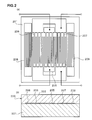
- Fig. 2(b) is a front cross-sectional view of the boundary acoustic wave device 200.
- the boundary acoustic wave device 200 has a laminated structure of a first medium 201 and a second medium 202.
- An input IDT 205, output IDTs 206 and 207, which function as electrodes, and reflectors 208 and 209 are disposed at the interface between the first and second media 201 and 202.
- Fig. 2(a) is a plan view showing the electrode structure.
- the first medium 201 was a 15° rotated Y-cut X-propagating LiNbO 3 substrate.
- a wavelength ⁇ based on the center-to-center distance of the IDTs 205 to 207 was 3.0 ⁇ m.
- the cross length of electrode fingers was 50 ⁇ .
- the input IDT 205 had 14.5 pairs of electrode fingers.
- the period of arrangement of the four outer electrode fingers of the IDT 205 in the propagation direction of a boundary wave was 0.86 ⁇ .
- the output IDTs 206 and 207 each had 8.5 pairs of electrode fingers, the period of arrangement of four electrode fingers adjacent to the input IDT 205 being 0.86 ⁇ .
- the reflectors 208 and 209 each had 41 electrode fingers and a period of arrangement of 1.033 ⁇ . Pass-band regions of the filter were disposed in reflection-band regions of the reflectors 208 and 209.
- the center-to-center distances of the nearest-neighbor electrodes between the input IDT 205 and each of the output IDTs 206 and 207 was 0.43 ⁇ .
- the center-to-center distance of the nearest-neighbor electrodes between the output IDT 206 and the reflector 208 and between the output IDT 207 and the reflector 209 was 0.5 ⁇ .
- the IDTs 205 to 207 and the reflectors 208 and 209 each had a duty ratio of 0.5.
- Fig. 3 is a schematic cross-sectional view illustrating the duty ratio.
- the term "duty ratio" means a value expressed as L/P in Fig. 3 , where L represents the width of an electrode finger; and P represents the center-to-center distance of the spaces between adjacent electrode fingers in the propagation direction of the boundary wave.
- the above-described electrodes were each formed of a laminate including an underlying NiCr film having a thickness of 0.003 ⁇ and a Au film having a thickness of 0.05 ⁇ disposed on the underlying NiCr film.
- the second medium was formed of a SiO 2 film.
- Two boundary acoustic wave devices described above were produced. That is, a first lot and a second lot of the boundary acoustic wave devices were obtained.
- the center frequency of the pass band of the filter needs to be matched to a target center frequency. Variation in the frequency of the pass band needs to be suppressed with high precision.
- a first lot and a second lot of the boundary acoustic wave devices were produced again in the same way as the first and second lots.
- the pass frequencies were measured before and after the formation of the SiO 2 films as the second media. Table 1 shows the results.
- the width of variation in frequency was as large as about 220 MHz before and after the formation of the SiO 2 film in each of the first and second lots.
- Comparison of a result of the boundary acoustic wave device of the first lot with that of the second lot showed that the frequency difference was further increased by 2 MHz after the formation of the SiO 2 film.
- the results demonstrate that production tolerance of the SiO 2 film, which is the second medium, significantly affects variation in the frequency of the final boundary acoustic wave device.
- the occurrence of variation in the second medium causes significant variation in the frequency of the boundary acoustic wave device.
- the frequency adjustment is performed after the formation of a second medium of a laminate.
- production tolerance in frequency is significantly reduced after the step of adjusting the frequency.
- a third medium is further formed, even when variation in the third medium occurs, variation in the frequency of the resulting boundary acoustic wave device is effectively suppressed. This will be explained with reference to Figs. 1 , 4, and 5 .
- Fig. 1 is a partially cutout front cross-sectional view of a boundary acoustic wave device according to an embodiment of the present invention.
- a second medium 2 and a third medium 3 are laminated on a first medium 1.
- Electrodes 5 are disposed at the interface between the first medium 1 and the second medium 2.
- the second medium 2 is formed, thus producing a laminate.
- the frequency adjustment is performed. More specifically, the frequency is adjusted by changing the thickness of the second medium 2.
- Examples of a method of changing the thickness of the second medium 2 include a method in which the second medium 2 is processed by etching or the like to reduce the thickness; and a method in which a film composed of a material identical to that of the second medium is formed by a film-forming process such as sputtering to substantially increase the thickness of the second medium 2.
- the thickness of the second medium 2 may be adjusted in the step of forming the second medium 2.
- the third medium 3 is formed.
- Methods for producing the second medium 2 and the third medium 3 are not limited to film-forming methods such as sputtering. Various methods may be employed. With respect to the third medium 3, a separately prepared film or a plate formed of the third medium may be bonded on the second medium 2.
- the third medium 3 needs to be different from the second medium 2 in terms of the sound velocity with which a boundary wave propagates therethrough and/or in terms of material.
- the sound velocity in the second medium 2 is identical to that of the third medium 3
- the material of the second medium 2 is identical to that of the third medium 3
- the frequency is not changed, in some cases.
- Fig. 4 shows the relationship between a schematic front cross-sectional view of a known boundary acoustic wave device and the energy distribution of a boundary acoustic wave.
- electrodes such as the input IDT 205 are disposed between the first medium 201 having a thickness of H1 and the second medium 202 having a thickness of H2.
- the energy of the boundary wave is concentrated on and around the interface.
- the energy decreases with distance from the interface.
- the energy is also present also in the hatched portion in Fig. 4 .
- the occurrence of the variation in the second medium after the formation of the second medium 202 results in variation in frequency.
- Fig. 5 shows the relationship between a schematic cross-sectional view of the boundary acoustic wave device of the above-described embodiment according to the first aspect of the present invention and the energy distribution of a boundary acoustic wave.
- the electrodes 5 are disposed at the interface between the first medium 1 having a thickness of H1 and the second medium 2 having a thickness of H2. In this case, the electrodes 5 are formed on the first medium 1. Then, the second medium 2 is formed. After the step of forming the second medium 2, the frequency adjustment is performed. After the frequency adjustment, the third medium 3 having a thickness of H3 is formed. In the resulting boundary acoustic wave device, after the step of forming the laminate having the first medium 1 and the second medium 2, the frequency adjustment is performed.
- the frequency adjustment before the formation of the third medium 3 can significantly reduce variation in the frequency of the boundary acoustic wave device after the formation of the third medium 3.
- Fig. 6 shows the relationship between a schematic cross-sectional view illustrating the reason for the small variation in the frequency of a boundary acoustic wave device according to the second aspect of the present invention and the energy distribution of a boundary acoustic wave.
- electrodes 25 are disposed between a first medium 21 having a thickness of H1 and a second medium 22 having a thickness of H2.
- a third medium 23 having a thickness of H3 is laminated thereon to form a laminate.
- the frequency adjustment is performed.
- a fourth medium 24 having a thickness of H4 is laminated on the third medium 23.
- the energy distribution of a boundary wave is shown at the right-hand side of Fig. 6 . That is, only part of the energy is distributed in the fourth medium.
- the frequency adjustment is performed to significantly reduce variation in frequency, even when the fourth medium 24 is further formed thereon, it is possible to suppress variation in frequency.
- the third medium 23 needs to be different from the fourth medium 24 in terms of the sound velocity with which a boundary wave propagates therethrough and/or in terms of material, otherwise the frequency is not changed.
- variation in frequency can be suppressed in the production process according to the first and second aspects of the present invention because the frequency adjustment is performed before the third or fourth medium formed at the end, and then the third or fourth medium is formed. That is, only part of the energy of a boundary wave is distributed in the third medium according to the first aspect of the present invention and the fourth medium according to the second aspect of the present invention.
- these production tolerance have less effect on variation in the frequency of a final boundary acoustic wave device. Therefore, it is possible to provide a boundary acoustic wave device having only small variation in frequency by performing the frequency adjustment after the step of forming the laminate.
- the second medium 22 may be composed of a material identical to that of the fourth medium 24 or may be composed of a material different from that of the fourth medium 24.
- the second medium 22 is composed of SiO 2 , which has a positive temperature coefficient of frequency
- combining SiO 2 with various materials each having a negative temperature coefficient of frequency can improve the temperature coefficient of frequency of the boundary wave device.
- the other is preferably composed of a material having a negative temperature coefficient of frequency other than SiO 2 .
- Both second and third media 2 and 3 may be composed of SiO 2 .
- either of the second medium 2 and the third medium 3 is preferably composed of SiO 2 .
- the third medium 23 may be composed of a material other than SiO 2 .
- the thickness H2 ( ⁇ ) of the second medium is preferably 1 ⁇ or less.
- the second medium has a thickness of 1 ⁇ or less, the energy of a boundary acoustic wave is negligibly distributed in the third medium; hence, it is possible to effectively reduce variation in frequency due to production tolerance in the third medium.
- the thickness H3 of the third medium preferably exceeds 0.5 ⁇ . At a thickness of the third medium exceeding 0.5 ⁇ , as shown in Fig. 5 , even when the energy of a boundary wave is distributed in the third medium, the energy of the boundary wave is surely reduced until the boundary wave reaches one surface of the third medium 3 opposite the other surface being in contact with the second medium 2, thereby resulting in satisfactory boundary wave propagation. In such a structure, even when foreign matter is attached on the surface, the characteristics of the boundary wave device are stable.
- the energy of a boundary wave is also distributed in the third medium.
- the energy of the boundary wave is also distributed in the fourth medium.
- the sound velocity in the third medium is different from those in the second and fourth media.
- adjusting the thickness of the third medium can regulate the sound velocity with which a boundary wave propagates therethrough.
- the energy of the boundary wave is surely reduced until the boundary wave reaches the surface of the medium 4 opposite the surface being in contact with the medium 3, thereby resulting in satisfactory boundary wave propagation.
- the characteristic of the boundary wave device are stable.
- a 15° rotated Y-cut X-propagating LiNbO 3 substrate was prepared as a first medium.
- the electrode structure shown in Fig. 2 was formed on the LiNbO 3 substrate. That is, the input IDT 205, the output IDTs 206 and 207, and the reflectors 208 and 209 shown in Fig. 2(a) were formed.
- the electrodes were made by the following procedure: after washing the LiNbO 3 substrate, a resist was spin-coated thereon, prebaked, and developed to form a resist pattern. A NiCr film and then a Au film were formed in that order by vacuum evaporation. The resist was lifted-off. The resulting electrodes were washed. Thereby, the electrode structure including the Au film having a thickness of 0.055 ⁇ and the NiCr film having a thickness of 0.001 ⁇ was obtained.
- a SiO 2 film functioning as a second medium and having a thickness of 0.1 ⁇ was formed over the surface having the electrodes of the LiNbO 3 substrate by RF sputtering, thereby producing a laminate shown in Fig. 2(b) .
- a resist was spin-coated on the SiO 2 film and then developed to form a resist pattern. Reactive ion etching and the removal of the resist were performed to remove the SiO 2 film disposed on the electrodes to be electrically connected with the exterior.
- the resulting exposed external terminals were brought into contact with probes of a wafer prober to measure a center frequency.
- the SiO 2 film was processed in such a manner that the resulting measurement corresponds to a target center frequency.
- the SiO 2 film was processed by a method in which the SiO 2 film was etched by reactive ion etching to reduce the thickness or a method in which a SiO 2 film was formed by sputtering to increase the thickness.
- the thickness of the SiO 2 film was reduced as described above. In contrast, when the measurement was higher than the target center frequency, the thickness of the SiO 2 film was increased.
- a propagating boundary wave was not a boundary acoustic wave but a surface acoustic wave, in which displacement was concentrated on the surface.
- the frequency adjustment was performed for the surface acoustic wave.
- a polycrystalline Si film having a thickness of 1 ⁇ was formed as a third medium by sputtering on the SiO 2 film.
- a propagating boundary wave was a boundary acoustic wave.
- a resist was spin-coated on the polycrystalline Si film, developed, baked, and patterned by reactive ion etching. The resist was removed, and then polycrystalline Si deposited on the external terminals was removed. Thereby, many boundary acoustic wave devices were produced.
- the resulting boundary acoustic wave devices have a small variation in resonant frequency.
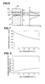
- Fig. 7 is a graph showing the relationship between the thickness H2 of the SiO 2 film of the boundary acoustic wave device produced in this example and the sound velocity, which is determined by multiplying the center frequency by ⁇ , in the boundary wave device.
- Fig. 8 is a graph showing the relationship between the thickness H2 of the SiO 2 film and the temperature coefficient of frequency (TCF)(ppm/°C).
- TCF temperature coefficient of frequency
- Fig. 7 clearly shows that the sound velocity decreases as the thickness of the SiO 2 film functioning as the second medium is increased.
- Fig. 8 clearly shows that the temperature coefficient of frequency (TCF) is improved as the thickness H2 of the SiO 2 film.
- a 15° rotated Y-cut X-propagating LiNbO 3 substrate was prepared as a first medium.
- the electrode structure shown in Fig. 2(a) was formed as in EXAMPLE 1.
- Many LiNbO 3 substrates each having the electrodes were prepared.
- a SiO 2 film was formed over the electrodes disposed on the LiNbO 3 substrate by RF sputtering.
- structures having the SiO 2 films with thicknesses of 0.1 ⁇ , 0.3 ⁇ , 0.5 ⁇ , and 1.0 ⁇ were produced.
- a polycrystalline Si film having a thickness of 0.5 ⁇ was formed on each SiO 2 film by RF sputtering.
- a laminate having a laminated structure of poly-Si/SiO 2/ electrodes/LiNbO 3 substrate, i.e., the laminate of third medium/second medium/electrodes/first medium was prepared.
- a propagating boundary wave was not a boundary acoustic wave but a surface acoustic wave, in which displacement was concentrated on the surface.
- the frequency adjustment was performed for the surface acoustic wave.
- a resist was spin-coated on the resulting polycrystalline Si film of the laminate, prebaked, and patterned. Reactive ion etching and the removal of the resist were performed to remove polycrystalline Si and SiO 2 disposed on external terminals, thereby exposing the external terminals. The exposed external terminals were brought into contact with probes of a wafer prober to measure a center frequency.
- the polycrystalline Si was processed in such a manner that the resulting measurement corresponds to a target center frequency.
- the polycrystalline Si was processed to reduce the thickness by reactive ion etching.
- polycrystalline Si film was formed again by sputtering to increase the thickness of the polycrystalline Si film.
- a SiO 2 film having a thickness of 1 ⁇ formed as a fourth medium by sputtering on the polycrystalline Si.
- a propagating boundary wave was a boundary acoustic wave.
- a resist was spin-coated on the SiO 2 film and patterned. Reactive ion etching and the removal of the resist were performed to remove the SiO 2 film disposed on the external electrodes. In this way, many boundary acoustic wave devices were produced.
- center frequencies of the resulting many boundary acoustic wave devices were measured. Variations in center frequencies of the boundary acoustic wave devices including the second media having thicknesses of 0.1 ⁇ , 0.3 ⁇ , 0.5 ⁇ , and 1.0 ⁇ decrease with increasing thickness.
- Fig. 9 is a graph showing the relationship between the thickness H3 of polycrystalline Si film, functioning as a third medium, of each of the boundary acoustic wave devices having the SiO 2 films, functioning as the second media, with thicknesses H2 of 0.1 ⁇ , 0.3 ⁇ , and 0.5 ⁇ and the sound velocity (center frequency ⁇ ⁇ ).
- Fig. 10 is a graph showing the relationship between the thickness H3 of a polycrystalline Si film and the temperature coefficient of frequency.
- the thickness of the SiO 2 film functioning as the fourth medium is unrelated to the sound velocity because of the boundary acoustic wave device.
- Fig. 9 clearly shows that the sound velocity is significantly changed within the range of 0 to 0.1 ⁇ in thickness of the polycrystalline Si film, and the frequency adjustment can be efficiently performed within the range.
- Fig. 10 clearly shows that the temperature coefficient of frequency (TCF) is improved up to 25 ppm/°C within the range compared with the temperature coefficient of frequency in EXAMPLE 1 shown in Fig. 8 .
- TCF temperature coefficient of frequency
- the thickness H2 of the second medium is preferably 0.5 ⁇ .
- the longitudinally coupled boundary acoustic wave resonator filter having a three-IDT structure shown in Fig. 2(a) has been described.
- the boundary acoustic wave devices according to the present invention may have various electrode structures. That is, a longitudinally coupled boundary acoustic wave resonator filter including two or more IDTs may be used.
- Fig. 11 which is a circuit diagram
- a ladder filter in which a plurality of boundary acoustic wave resonators S1, S2, P1, and P2 are connected may be used. While four boundary acoustic wave resonators are connected
- a ladder filter including a desired number of stages may be used.
- the number of resonators in the ladder filter is not particularly limited.
- a laterally coupled boundary acoustic wave filter may be used.
- a comb-shape transducer (see “Dansei Hyomenha Kogaku", published by Institute of Electronics, Information and Communication Engineers, sixth impression of the first edition, page 57) may be used as the electrode, in place of the IDT.
- ⁇ is defined as the period of arrangement of strips of the comb-shape transducer. That is, a wavelength at which an electroacoustic transducer is excited may be defined as ⁇ .
- the electrode is formed of the laminate including the Au electrode layer as a main component and the underlying NiCr layer.
- the electrode may be composed of other metals.
- the electrode may be composed of one metal selected from Ag, Cu, Fe, Ta, W, Ti, and Pt.
- a second thin electrode layer composed of Ti, Cr, NiCr, or the like may be laminated.
- the second electrode layer may be disposed between the first medium and the electrode layer mainly composed of Au or the like.
- the second electrode layer may be disposed between the main electrode layer and the second medium.
- the electrode may have a structure in which three or more electrode layers are laminated. In this case, the second electrode layer may be laminated as an interlayer.
- the electrode structure may be composed of an alloy of a plurality of metals.
- the materials constituting the first to third media and the first to fourth media according to the present invention are not particularly limited. That is, various dielectrics may be used as the media.
- An example thereof is one material selected from the group consisting of lithium niobate, potassium niobate, lithium tantalate, lithium tetraborate, langasite, langanite, quartz, lead zirconate titanate ceramics, ZnO, AlN, silicon oxides, glass, silicon, sapphire, silicon nitrides, and carbon nitrides.
- the medium is not necessarily composed of a single material but may have a laminated structure in which a plurality of medium layers are laminated. That is, at least one medium among the first to third media and the first to fourth media may have the laminated structure in which a plurality of medium layers are laminated.
- a protective layer for enhancing strength and preventing the penetration of corrosive gas and the like may be formed at the outer side.
- the boundary acoustic wave device may be housed in a package if increased size of the component does not cause problems.
- the protective layer may be composed of an insulating material, such as titanium oxide, aluminum nitride, or aluminum oxide; a metal, such as Au, Al, or W; or a resin such as an epoxy resin.
- an insulating material such as titanium oxide, aluminum nitride, or aluminum oxide
- a metal such as Au, Al, or W
- a resin such as an epoxy resin.
Landscapes
- Physics & Mathematics (AREA)
- Acoustics & Sound (AREA)
- Engineering & Computer Science (AREA)
- Manufacturing & Machinery (AREA)
- Surface Acoustic Wave Elements And Circuit Networks Thereof (AREA)
Abstract
Description
- The present invention relates to a boundary acoustic wave device using a boundary acoustic wave propagating through the interface between media and a process for producing the boundary acoustic wave device. Specifically, the present invention relates to a boundary acoustic wave device having a structure including electrodes disposed between a first medium and a second medium; and another medium laminated on the outer surface of one of the first and second media, and also relates to a process for producing the boundary acoustic wave device.
- Heretofore, various surface acoustic wave devices have been used for RF and IF filters in mobile phones, resonators in VCOs, and VIF filters in television sets. The surface acoustic wave devices each use a surface acoustic wave, such as a Rayleigh wave or a first-order leaky wave, propagating along a surface of a medium.
- Surface acoustic waves propagate along the surface of a medium and are thus sensitive to change in the surface condition of the medium. Accordingly, to protect the surface of the medium along which the surface acoustic waves propagate, in the related art, the surface acoustic wave element is hermetically sealed in a package having a cavity such that the surface of the medium described above is placed therein. The use of the package having the cavity inevitably increases the cost of the surface acoustic wave device. In addition, the package has significantly larger dimensions than the surface acoustic wave element; hence, the surface acoustic wave device inevitably has a large size.
- Acoustic waves other than the surface acoustic waves include boundary acoustic waves propagating along the boundaries between solids.
- For example, Non-Patent
Document 1 discloses a boundary acoustic wave device including an IDT disposed on a 126°-rotated Y-plate X-propagating LiTaO3 substrate and a SiO2 film with a predetermined thickness over the IDT and the LiTaO3 substrate. This document describes that SV + P mode boundary acoustic waves called Stoneley waves propagate. Non-PatentDocument 1 also describes that when the SiO2 film has a thickness of 1.0 λ (wherein λ represents the wavelength of the boundary acoustic wave), the electromechanical coupling coefficient is 2%. - Boundary acoustic waves propagate with their energy concentrated on the boundaries between the solids. Thus, little energy is present on the bottom surface of the LiTaO3 substrate and a surface of the SiO2 film. Therefore, characteristics of the boundary acoustic wave do not vary with changes in the surface state of the substrate or the thin film. Thus, a package having a cavity is unnecessary, thereby reducing the size of the acoustic wave device.
- To suppress non-uniformities in resonant frequencies and center frequencies in filters and resonators using the acoustic waves, various methods for adjusting frequencies have been developed. For examples,
Patent Document 1 discloses, in a piezoelectric ceramic filter using the thickness vibration of a bulk wave, a method for adjusting a frequency by evaporation of an insulating material onto resonant electrodes disposed on a surface of a piezoelectric ceramic substrate. -
Patent Document 2 discloses a surface wave device using a surface wave, the surface wave device including a SiN film covering interdigital electrodes and reflectors disposed on a piezoelectric substrate. A center frequency and a resonant frequency are adjusted by controlling the thickness of the SiN film. -
Patent Document 3 discloses a boundary acoustic wave device shown inFig. 12 . A boundary acoustic wave device 100 includesinterdigital electrodes piezoelectric substrate 101; adielectric film 103 over theinterdigital electrodes second substrate 104 laminated on the upper surface of thedielectric film 103. In the boundary acoustic wave device 100, the Si-basedsecond substrate 104 is disposed on theinterdigital electrodes 102 with thedielectric film 103 provided therebetween and thus is not in direct contact with theinterdigital electrodes interdigital electrodes - Non-Patent Document 1: "Piezoelectric Acoustic Boundary Waves Propagating Along the Interface between SiO2 and LiTa03" IEEE Trans. Sonics and ultrason., vol. SU-25, No.6, 1978 IEEE
- Patent Document 1: Japanese Unexamined Patent Application Publication No.
5-191193 - Patent Document 2: Japanese Unexamined Patent Application Publication No.
2-301210 - Patent Document 3:
WO98/51011 - The above-described boundary acoustic wave device does not require a package having a cavity, thereby reducing the size of an acoustic wave device. However, according to experiments conducted by the inventors, production tolerance often induced nonuniformities in a resonant frequency and a center frequency in the boundary acoustic wave devices, as in the case of the surface acoustic wave devices. In particular, in the boundary acoustic wave device, after the formation of the electrodes on a first medium, a second medium was formed so as to cover the electrodes. Thus, if there was production tolerance in the second medium, the frequency of the boundary acoustic wave device would have been liable to vary significantly.
- On the other hand, in methods described in
Patent Documents Patent Document 2, a SiN film is provided on a surface wave substrate to adjust the frequency. That is, in a known bulk wave device and surface acoustic wave device, an insulating material or a metal is deposited on a surface of a substrate to adjust a frequency by using the distribution of oscillation energy to the surface of the substrate. Furthermore, in another method, an electrode disposed on a surface of a substrate is etched or a surface of a substrate is etched to adjust a frequency. - However, since the oscillation energy of a boundary wave is negligibly distributed in a boundary acoustic wave device, such a method for adjusting the frequency cannot be employed. In other words, if foreign matter such as an insulating material is deposited on a surface of a substrate or if a surface of a substrate is etched, the resonant frequency and a pass band are not changed.
- In the boundary acoustic wave device 100 described in
Patent Document 3, interposing thedielectric film 103 reduces parasitic resistance. However, the frequency cannot be adjusted after completion. - In consideration of the above-described situation, it is an object of the present invention to provide a process for stably and surely producing a boundary acoustic wave device having target frequency characteristics, the process being able to efficiently suppress variation in frequency due to production tolerance. It is another object of the present invention to provide a boundary acoustic wave device having target frequency characteristics with only slight nonuniformity in frequency from lot to lot.
- According to a first aspect of the present invention, in a process for producing a boundary acoustic wave device that includes a first medium, a second medium, and a third medium laminated in that order; and electrodes disposed at the interface between the first medium and the second medium, the process includes the steps of preparing a laminate including the first medium, the second medium, and the electrodes disposed at the interface between the first medium and the second medium; adjusting the thickness of the second medium after the step of preparing the laminate to regulate a frequency or the sound velocity of a surface acoustic wave, a pseudo-boundary acoustic wave, or a boundary acoustic wave; and after the adjusting step, forming the third medium different from the second medium in terms of the sound velocity with which the boundary acoustic wave propagates therethrough and/or in terms of material.
- According to an embodiment of the first aspect of the present invention, the third medium has a thickness exceeding 0.5 λ, where λ represents the wavelength of the boundary acoustic wave.
- According to a second aspect of the present invention, in a process for producing a boundary acoustic wave device that includes a first medium, a second medium, a third medium, and a fourth medium laminated in that order; and electrodes disposed at the interface between the first medium and the second medium, the process includes the steps of preparing a laminate including the first medium, the second medium, and the third medium formed in that order and electrodes disposed at the interface between the first medium and the second medium; adjusting a frequency or the sound velocity of a surface acoustic wave, a pseudo-boundary acoustic wave, or a boundary acoustic wave after the step of preparing the laminate; and after the adjusting step, forming the fourth medium, the sound velocity in the fourth medium and/or the material of the fourth medium being different from that of the third medium.
- In the first and second aspects of the present invention described above, the sound velocity in the third medium and/or the material of the third medium is different from that of the second medium, and sound velocity in the fourth medium and/or the material of fourth medium is different from the third medium. In this case, different materials result in different sound velocities of a longitudinal wave and a transverse wave. When the same material is used, it is possible to change the sound velocity by using different crystalline states or by changing the degree of density if the material is polycrystalline. Furthermore, when the medium layer is isotropic, the velocity of longitudinal waves in the medium layer, i.e., Vs, and the velocity of transverse waves, i.e., Vp, are represented by equations (1) and (2):


where C11 and C12 each represent an elastic stiffness constant; and ρ represents a density. According to an embodiment of the second aspect of the present invention, the fourth medium has a thickness exceeding 0.5 λ, where λ represents the wavelength of a boundary acoustic wave. - According to another embodiment of the first or second aspect of the present invention, at least one medium has a laminated structure in which a plurality of material layers are laminated.
- According to another embodiment of the first or second aspect of the present invention, the electrodes are each composed of one metal selected from the group consisting of Au, Ag, Cu, Fe, Ta, W, Ti, and Pt.
- According to another embodiment of the first or second aspect of the present invention, the medium layers are each composed of at least one material selected from the group consisting of lithium niobate, potassium niobate, lithium tantalate, lithium tetraborate, langasite, langanite, quartz, lead zirconate titanate ceramics, ZnO, AlN, silicon oxides, glass, silicon, sapphire, silicon nitrides, and carbon nitrides.
- According to another embodiment of the first or second aspect of the present invention, the electrodes constitute a boundary acoustic wave resonator or a boundary acoustic wave filter, and the boundary acoustic wave device is the boundary acoustic wave resonator or the boundary acoustic wave filter.
- According to a third aspect of the present invention, a boundary acoustic wave device includes a first medium, a second medium, a third medium, and a fourth medium laminated in that order; and electrodes disposed at the interface between the first medium and the second medium, the sound velocity in the third medium and/or the material of the third medium being different from that of the fourth medium.
- In the production process according to the first aspect of the present invention, after preparing the laminate including the first medium, the second medium, and the electrodes disposed at the interface between the first medium and the second medium, the thickness of the second medium is adjusted after the step of preparing the laminate to regulate a frequency or the sound velocity of a boundary acoustic wave. After the adjusting step, the third medium is formed, the third medium being different from the second medium in terms of the sound velocity with which the boundary acoustic wave propagates therethrough and/or in terms of material. That is, the laminate including the electrodes disposed between the first and the second media is prepared, and then the second thickness is adjusted after the step of preparing the laminate. Thereby, it is possible to regulate a frequency or the sound velocity of a surface acoustic wave, a pseudo-boundary acoustic wave, or a boundary acoustic wave. Thus, it is possible to produce a laminate for forming a boundary acoustic wave device having a target frequency. In this case, to adjust the second medium after the step of preparing the laminate to regulate the frequency or the sound velocity, the thickness of the second medium may be adjusted in producing the laminate. Alternatively, the thickness of the second medium may be changed after the completion of the laminate.
- After the adjusting step, the third medium, in which the sound velocity in the third medium and/or the material of the third medium is different from that of the second medium, is formed. The energy of the boundary acoustic wave is negligibly distributed in the third medium. Thus, even if variation of the third medium from lot to lot occurs, variations in sound velocity and frequency do not easily occur. Consequently, it is possible to easily and reliably provide a boundary acoustic wave device having only slight nonuniformity in device characteristics.
- In the production process according to the first aspect of the present invention, after preparing the laminate including the first medium, the second medium, and the third medium formed in that order and electrodes disposed at the interface between the first medium and the second medium, the thickness of the third medium is adjusted after the step of preparing the laminate to regulate a frequency or the sound velocity of a boundary acoustic wave. After the adjusting step, the fourth medium is formed, the sound velocity in the fourth medium and/or the material of the fourth medium being different from that of the third medium. That is, the laminate including the electrodes disposed between the first and the second media; and the third medium laminated on the second medium is prepared, and then the thickness of the third medium is adjusted after the step of preparing the laminate. Thereby, it is possible to regulate a frequency or the sound velocity of a surface acoustic wave, a pseudo-boundary acoustic wave, or a boundary acoustic wave. Thus, it is possible to produce a laminate for forming a boundary acoustic wave device having a target frequency. In this case, to adjust the third medium after the step of preparing the laminate to regulate the frequency or the sound velocity, the thickness of the third medium may be adjusted in producing the laminate. Alternatively, the thickness of the third medium may be changed after the completion of the laminate.
- After the adjusting step, the fourth medium, in which the sound velocity in the fourth medium and/or the material of the fourth medium is different from that of the third medium, is formed. The energy of the boundary acoustic wave is negligibly distributed in the fourth medium. Thus, even if variation of the fourth medium from lot to lot occurs, variations in sound velocity and frequency do not easily occur. Consequently, it is possible to easily and reliably provide a boundary acoustic wave device having only slight nonuniformity in device characteristics.
- In a boundary wave propagating through the boundary acoustic wave device according to the first or second aspect of the present invention, most of the energy is distributed in the range up to 0.5 λ thickness of a medium 3 in the first aspect or a medium 4 in the second aspect of the present invention. Thus, the medium 3 in the first aspect or the medium 4 in the second aspect of the present invention preferably has a thickness of 0.5 λ or more.
- When at least one medium has a laminated structure in which a plurality of material layers are laminated, the selection of the plurality of the material layers can easily form medium layers having different sound velocities therein or frequency characteristics.
- When the electrodes are each composed of one metal selected from the group consisting of Au, Ag, Cu, Fe, Ta, W, Ti, and Pt, the metal is used as a material for the propagation path, the IDT, and the reflector of the boundary wave device.
- In the medium layers each composed of at least one material selected from the group consisting of lithium niobate, potassium niobate, lithium tantalate, lithium tetraborate, langasite, langanite, quartz, lead zirconate titanate ceramics, ZnO, AlN, silicon oxides, glass, silicon, sapphire, silicon nitrides, and carbon nitrides, the thickness of the metal material and duty ratios of the IDT and the reflector are adjusted in such a manner that the sound velocity of the boundary wave is lower than those in the materials of the media, thereby producing a boundary wave device.
- When the electrodes constitute a boundary acoustic wave resonator or a boundary acoustic wave filter, the boundary acoustic wave resonator or the boundary acoustic wave filter can be produced according to the present invention.
- In the boundary acoustic wave device according to the present invention, the first medium, the second medium, and the third medium are laminated in that order. The electrodes are disposed at the interface between the first and second media. The sound velocity in the second medium and/or the material of the second medium is different from that of the third medium. The energy of the boundary wave is distributed as shown in
Fig. 5 . Thus, changing the thickness of the second medium can adjust the sound velocity with which the boundary wave propagates therethrough. Changing the thickness of the third medium cannot adjust the sound velocity with which the boundary wave propagates therethrough because the energy of the boundary wave is not distributed on the surface of the third medium. An operating frequency F of the boundary wave device is expressed as F = V/λ, where V represents the sound velocity of a boundary wave; and λ represents the period of IDT strips. Thus, adjusting the sound velocity can regulate the operating frequency of the boundary wave device. - In the third aspect of the present invention, the first medium, the second medium, the third medium, and the fourth medium are laminated in that order. The electrodes are disposed at the interface between the first and second media. The sound velocity in the third medium and/or the material of the third medium is different from that of the fourth medium. The energy of the boundary wave is distributed as shown in
Fig. 6 . Thus, changing the thickness of the third medium can adjust the sound velocity with which the boundary wave propagates therethrough. Changing the thickness of the fourth medium cannot adjust the sound velocity with which the boundary wave propagates therethrough because the energy of the boundary wave is not distributed on the surface of the fourth medium. An operating frequency F of the boundary wave device is expressed as F = V/λ, where V represents the sound velocity of a boundary wave; and λ represents the period of IDT strips. Thus, adjusting the sound velocity can regulate the operating frequency of the boundary wave device. - In the third aspect of the present invention, the second and fourth media may be composed of the same material, thereby improving various characteristics. In general, many dielectric materials and metal materials have negative temperature coefficients of sound velocities of acoustic waves. When the first to third media and the electrode layer are each composed of a material having a negative temperature coefficient, the boundary acoustic wave has a negative temperature coefficient. The temperature coefficient of operating frequency of a boundary acoustic wave device, i.e., TCF, is expressed as:

where V represents the sound velocity of a boundary wave; ΔV represents the width of variation in sound velocity; AT represents the width of variation in temperature; and α represents a coefficient of linear thermal expansion. Many dielectric materials and metal materials have positive coefficients of linear thermal expansion. Thus, the boundary acoustic wave device has a negative TCF. In the boundary acoustic wave device, the TCF is preferably zero. - To improve the temperature characteristics, the second and fourth media may be each composed of SiO2 having a positive temperature coefficient. In this case, it is possible to bring the temperature coefficient closer to zero compared with the case in which the second medium is composed of a dielectric material having a negative temperature coefficient. Furthermore, the appropriate selection of the materials of the first and third media and the thickness of each media can bring the TCF to zero.
-
-
Fig. 1 is a schematic front cross-sectional view illustrating a boundary acoustic wave device according to an embodiment of the present invention. -
Fig. 2(a) is a plan view showing an electrode structure of a boundary acoustic wave device according to the present invention, andFig. 2(b) is a front cross-sectional view of the boundary acoustic wave device. -
Fig. 3 is a schematic fragmentary enlarged cross-sectional view illustrating duty ratios of the IDT and reflectors of a boundary acoustic wave device. -
Fig. 4 shows the relationship between the cross-sectional structure of a known boundary acoustic wave device and the energy distribution of a boundary acoustic wave. -
Fig. 5 shows the relationship between a cross-sectional structure of a boundary acoustic wave device according to a first aspect of the present invention and the energy distribution of a boundary acoustic wave. -
Fig. 6 shows the relationship between a cross-sectional structure of a boundary acoustic wave device according to a second aspect of the present invention and the energy distribution of a boundary acoustic wave. -
Fig. 7 is a graph showing the relationship between the thickness H2 of a SiO2 film, which is a second medium of a boundary acoustic wave device in Example 1, and the sound velocity (center frequency × λ). -
Fig. 8 is a graph showing the relationship between the thickness H2 of a SiO2 film, which is a second medium of a boundary acoustic wave device in Example 1, and the temperature coefficient of frequency. -
Fig. 9 is a graph showing the relationship between the thickness H3 of a polycrystalline Si film, which is a third medium of a boundary acoustic wave device in Example 2, and the sound velocity (center frequency × λ). -
Fig. 10 is a graph showing the relationship between the thickness H3 of a polycrystalline Si film, which is a third medium of a boundary acoustic wave device in Example 2, and the temperature coefficient of frequency. -
Fig. 11 is a circuit diagram of a ladder filter as an example of a boundary acoustic wave device according to the present invention. -
Fig. 12 is a perspective view illustrating an example of a known boundary acoustic wave device. -
Fig. 13 is a graph showing frequency characteristics of the known boundary acoustic wave device and shows production tolerance in frequency. -
- 1
- first medium
- 2
- second medium
- 3
- third medium
- 5
- electrode
- 20
- boundary acoustic wave device
- 21
- first medium
- 22
- second medium
- 23
- third medium
- 24
- fourth medium
- 25
- electrode
- The present invention will be explained by describing specific embodiments according to the present invention with reference to the drawings.
- The inventors have produced a boundary acoustic wave device shown in
Figs. 2(a) and 2(b) and studied the device.Fig. 2(b) is a front cross-sectional view of the boundaryacoustic wave device 200. The boundaryacoustic wave device 200 has a laminated structure of afirst medium 201 and asecond medium 202. Aninput IDT 205,output IDTs reflectors second media Fig. 2(a) is a plan view showing the electrode structure. - In the boundary
acoustic wave device 200, thefirst medium 201 was a 15° rotated Y-cut X-propagating LiNbO3 substrate. A wavelength λ based on the center-to-center distance of theIDTs 205 to 207 was 3.0 µm. The cross length of electrode fingers was 50 λ. Theinput IDT 205 had 14.5 pairs of electrode fingers. The period of arrangement of the four outer electrode fingers of theIDT 205 in the propagation direction of a boundary wave was 0.86 λ. Theoutput IDTs input IDT 205 being 0.86 λ. Thereflectors reflectors input IDT 205 and each of the output IDTs 206 and 207 was 0.43 λ. The center-to-center distance of the nearest-neighbor electrodes between theoutput IDT 206 and thereflector 208 and between theoutput IDT 207 and thereflector 209 was 0.5 λ. TheIDTs 205 to 207 and thereflectors -
Fig. 3 is a schematic cross-sectional view illustrating the duty ratio. The term "duty ratio" means a value expressed as L/P inFig. 3 , where L represents the width of an electrode finger; and P represents the center-to-center distance of the spaces between adjacent electrode fingers in the propagation direction of the boundary wave. The period of arrangement of the IDT and the reflector, i.e., λ, is expressed as λ = 2 × P. - The above-described electrodes were each formed of a laminate including an underlying NiCr film having a thickness of 0.003 λ and a Au film having a thickness of 0.05 λ disposed on the underlying NiCr film. The second medium was formed of a SiO2 film.
- Two boundary acoustic wave devices described above were produced. That is, a first lot and a second lot of the boundary acoustic wave devices were obtained.
- S21 characteristics (transmission characteristics) of the boundary acoustic wave devices of the first and second lots were measured. As shown in
Fig. 13 , the results demonstrated that the mean center frequency of the pass band of the first lot was different from that of the second lot by 5.6 MHz. - The center frequency of the pass band of the filter needs to be matched to a target center frequency. Variation in the frequency of the pass band needs to be suppressed with high precision. A first lot and a second lot of the boundary acoustic wave devices were produced again in the same way as the first and second lots. The pass frequencies were measured before and after the formation of the SiO2 films as the second media. Table 1 shows the results.
Table 1 First lot Second lot Before formation of SiO2 film 844 MHz 847 MHz After formation of SiO2 film 1,060 MHz 1,065MHz - As is apparent from Table 1, the width of variation in frequency was as large as about 220 MHz before and after the formation of the SiO2 film in each of the first and second lots. Comparison of a result of the boundary acoustic wave device of the first lot with that of the second lot showed that the frequency difference was further increased by 2 MHz after the formation of the SiO2 film. Thus, the results demonstrate that production tolerance of the SiO2 film, which is the second medium, significantly affects variation in the frequency of the final boundary acoustic wave device.
- In the case of the formation of the SiO2 film functioning as the second medium after the formation of the electrodes on the first medium as described above, the occurrence of variation in the second medium causes significant variation in the frequency of the boundary acoustic wave device.
- In contrast, according to the first aspect of the present invention, the frequency adjustment is performed after the formation of a second medium of a laminate. Thus, production tolerance in frequency is significantly reduced after the step of adjusting the frequency. In the case in which a third medium is further formed, even when variation in the third medium occurs, variation in the frequency of the resulting boundary acoustic wave device is effectively suppressed. This will be explained with reference to
Figs. 1 ,4, and 5 . -
Fig. 1 is a partially cutout front cross-sectional view of a boundary acoustic wave device according to an embodiment of the present invention. In this boundary acoustic wave device, asecond medium 2 and athird medium 3 are laminated on afirst medium 1.Electrodes 5 are disposed at the interface between thefirst medium 1 and thesecond medium 2. In this embodiment, after the formation of theelectrodes 5 on the first medium, thesecond medium 2 is formed, thus producing a laminate. After the step of forming the laminate, the frequency adjustment is performed. More specifically, the frequency is adjusted by changing the thickness of thesecond medium 2. Examples of a method of changing the thickness of thesecond medium 2 include a method in which thesecond medium 2 is processed by etching or the like to reduce the thickness; and a method in which a film composed of a material identical to that of the second medium is formed by a film-forming process such as sputtering to substantially increase the thickness of thesecond medium 2. Alternatively, the thickness of thesecond medium 2 may be adjusted in the step of forming thesecond medium 2. - In this embodiment, after the thickness adjustment, the
third medium 3 is formed. - Methods for producing the
second medium 2 and thethird medium 3 are not limited to film-forming methods such as sputtering. Various methods may be employed. With respect to thethird medium 3, a separately prepared film or a plate formed of the third medium may be bonded on thesecond medium 2. - In the boundary acoustic wave device according to the first aspect of the present invention, the
third medium 3 needs to be different from thesecond medium 2 in terms of the sound velocity with which a boundary wave propagates therethrough and/or in terms of material. In the case where the sound velocity in thesecond medium 2 is identical to that of thethird medium 3, and where the material of thesecond medium 2 is identical to that of thethird medium 3, even when the above-described step of adjusting the frequency is performed, the frequency is not changed, in some cases. -
Fig. 4 shows the relationship between a schematic front cross-sectional view of a known boundary acoustic wave device and the energy distribution of a boundary acoustic wave. As is apparent fromFig. 4 , in the boundaryacoustic wave device 200, electrodes such as theinput IDT 205 are disposed between thefirst medium 201 having a thickness of H1 and thesecond medium 202 having a thickness of H2. As shown at the right-hand side ofFig. 4 , the energy of the boundary wave is concentrated on and around the interface. In the first andsecond media second medium 202, the energy is also present also in the hatched portion inFig. 4 . Thus, the occurrence of the variation in the second medium after the formation of thesecond medium 202 results in variation in frequency. -
Fig. 5 shows the relationship between a schematic cross-sectional view of the boundary acoustic wave device of the above-described embodiment according to the first aspect of the present invention and the energy distribution of a boundary acoustic wave. - In the boundary acoustic wave device shown in
Fig. 5 , theelectrodes 5 are disposed at the interface between thefirst medium 1 having a thickness of H1 and thesecond medium 2 having a thickness of H2. In this case, theelectrodes 5 are formed on thefirst medium 1. Then, thesecond medium 2 is formed. After the step of forming thesecond medium 2, the frequency adjustment is performed. After the frequency adjustment, thethird medium 3 having a thickness of H3 is formed. In the resulting boundary acoustic wave device, after the step of forming the laminate having thefirst medium 1 and thesecond medium 2, the frequency adjustment is performed. - With respect to the energy distribution of the boundary wave in the boundary acoustic wave device, only part of energy is distributed in the
third medium 3 as shown at the right-hand side ofFig. 5 . Thus, even when variation in the third medium 3 from production tolerance occurs, nonuniformity in frequency due to the variation is very small. Therefore, the frequency adjustment before the formation of thethird medium 3 can significantly reduce variation in the frequency of the boundary acoustic wave device after the formation of thethird medium 3. -
Fig. 6 shows the relationship between a schematic cross-sectional view illustrating the reason for the small variation in the frequency of a boundary acoustic wave device according to the second aspect of the present invention and the energy distribution of a boundary acoustic wave. - In a boundary
acoustic wave device 20 according to the second aspect of the present invention,electrodes 25 are disposed between a first medium 21 having a thickness of H1 and a second medium 22 having a thickness of H2. A third medium 23 having a thickness of H3 is laminated thereon to form a laminate. After step of forming the laminate, the frequency adjustment is performed. A fourth medium 24 having a thickness of H4 is laminated on thethird medium 23. In the resulting boundaryacoustic wave device 20, the energy distribution of a boundary wave is shown at the right-hand side ofFig. 6 . That is, only part of the energy is distributed in the fourth medium. Thus, in the case where after the step of forming the laminate having the third medium 23, the frequency adjustment is performed to significantly reduce variation in frequency, even when thefourth medium 24 is further formed thereon, it is possible to suppress variation in frequency. - In the second aspect of the present invention, the third medium 23 needs to be different from the fourth medium 24 in terms of the sound velocity with which a boundary wave propagates therethrough and/or in terms of material, otherwise the frequency is not changed.
- As described above, variation in frequency can be suppressed in the production process according to the first and second aspects of the present invention because the frequency adjustment is performed before the third or fourth medium formed at the end, and then the third or fourth medium is formed. That is, only part of the energy of a boundary wave is distributed in the third medium according to the first aspect of the present invention and the fourth medium according to the second aspect of the present invention. Thus, even when production tolerance in the third medium according to the first aspect of the present invention and production tolerance in the fourth medium according to the second aspect of the present invention occur, these production tolerance have less effect on variation in the frequency of a final boundary acoustic wave device. Therefore, it is possible to provide a boundary acoustic wave device having only small variation in frequency by performing the frequency adjustment after the step of forming the laminate.
- In the second aspect of the present invention, the second medium 22 may be composed of a material identical to that of the fourth medium 24 or may be composed of a material different from that of the
fourth medium 24. For example, in the case where thesecond medium 22 is composed of SiO2, which has a positive temperature coefficient of frequency, combining SiO2 with various materials each having a negative temperature coefficient of frequency can improve the temperature coefficient of frequency of the boundary wave device. In the first aspect of the present invention, when one of thesecond medium 2 and thethird medium 3 is composed of SiO2, the other is preferably composed of a material having a negative temperature coefficient of frequency other than SiO2. Both second andthird media second medium 2 and thethird medium 3 is preferably composed of SiO2. - In the second aspect of the present invention, when the
second medium 22 and the fourth medium 24 are each composed of SiO2, the third medium 23 may be composed of a material other than SiO2. Thus, it is possible to perform the frequency adjustment while maintaining the effect of improving the temperature coefficient of frequency. - In the first aspect of the present invention, the thickness H2 (λ) of the second medium is preferably 1 λ or less. When the second medium has a thickness of 1 λ or less, the energy of a boundary acoustic wave is negligibly distributed in the third medium; hence, it is possible to effectively reduce variation in frequency due to production tolerance in the third medium. Furthermore, the thickness H3 of the third medium preferably exceeds 0.5 λ. At a thickness of the third medium exceeding 0.5 λ, as shown in
Fig. 5 , even when the energy of a boundary wave is distributed in the third medium, the energy of the boundary wave is surely reduced until the boundary wave reaches one surface of thethird medium 3 opposite the other surface being in contact with thesecond medium 2, thereby resulting in satisfactory boundary wave propagation. In such a structure, even when foreign matter is attached on the surface, the characteristics of the boundary wave device are stable. - In the second aspect of the present invention, at a thickness H2 of the second medium of 0.5 λ or less, as shown in
Fig. 6 , the energy of a boundary wave is also distributed in the third medium. Furthermore, at a thickness H3 of the third medium of 0.1 λ or less, the energy of the boundary wave is also distributed in the fourth medium. The sound velocity in the third medium is different from those in the second and fourth media. Thus, adjusting the thickness of the third medium can regulate the sound velocity with which a boundary wave propagates therethrough. When the energy of a boundary wave is not distributed in the third medium because the second medium has a large thickness, the sound velocity with which the boundary wave propagates therethrough cannot be regulated by changing the state of the third medium. When the energy of the boundary wave is not distributed in the fourth medium because the third medium has a large thickness, the sound velocity with which the boundary wave propagates therethrough cannot be regulated by changing the thickness of the fourth medium. - As shown in
Fig. 6 , the energy of the boundary wave is surely reduced until the boundary wave reaches the surface of the medium 4 opposite the surface being in contact with themedium 3, thereby resulting in satisfactory boundary wave propagation. In such a structure, even when foreign matter is attached on the surface, the characteristic of the boundary wave device are stable. - Specific examples will be described below.
- A 15° rotated Y-cut X-propagating LiNbO3 substrate was prepared as a first medium. The electrode structure shown in
Fig. 2 was formed on the LiNbO3 substrate. That is, theinput IDT 205, the output IDTs 206 and 207, and thereflectors Fig. 2(a) were formed. The electrodes were made by the following procedure: after washing the LiNbO3 substrate, a resist was spin-coated thereon, prebaked, and developed to form a resist pattern. A NiCr film and then a Au film were formed in that order by vacuum evaporation. The resist was lifted-off. The resulting electrodes were washed. Thereby, the electrode structure including the Au film having a thickness of 0.055 λ and the NiCr film having a thickness of 0.001 λ was obtained. - Next, a SiO2 film functioning as a second medium and having a thickness of 0.1 λ was formed over the surface having the electrodes of the LiNbO3 substrate by RF sputtering, thereby producing a laminate shown in
Fig. 2(b) . - A resist was spin-coated on the SiO2 film and then developed to form a resist pattern. Reactive ion etching and the removal of the resist were performed to remove the SiO2 film disposed on the electrodes to be electrically connected with the exterior.
- The resulting exposed external terminals were brought into contact with probes of a wafer prober to measure a center frequency. The SiO2 film was processed in such a manner that the resulting measurement corresponds to a target center frequency. In this step, the SiO2 film was processed by a method in which the SiO2 film was etched by reactive ion etching to reduce the thickness or a method in which a SiO2 film was formed by sputtering to increase the thickness.
- That is, when the measurement was lower than the target center frequency, the thickness of the SiO2 film was reduced as described above. In contrast, when the measurement was higher than the target center frequency, the thickness of the SiO2 film was increased.
- At this point, a propagating boundary wave was not a boundary acoustic wave but a surface acoustic wave, in which displacement was concentrated on the surface. The frequency adjustment was performed for the surface acoustic wave.
- After the frequency adjustment, a polycrystalline Si film having a thickness of 1 λ was formed as a third medium by sputtering on the SiO2 film.
- At this point, a propagating boundary wave was a boundary acoustic wave.
- A resist was spin-coated on the polycrystalline Si film, developed, baked, and patterned by reactive ion etching. The resist was removed, and then polycrystalline Si deposited on the external terminals was removed. Thereby, many boundary acoustic wave devices were produced.
- The resulting boundary acoustic wave devices have a small variation in resonant frequency.
-
Fig. 7 is a graph showing the relationship between the thickness H2 of the SiO2 film of the boundary acoustic wave device produced in this example and the sound velocity, which is determined by multiplying the center frequency by λ, in the boundary wave device.Fig. 8 is a graph showing the relationship between the thickness H2 of the SiO2 film and the temperature coefficient of frequency (TCF)(ppm/°C). The thickness of the polycrystalline Si film functioning as the third medium is unrelated to the sound velocity because of the boundary acoustic wave device. -
Fig. 7 clearly shows that the sound velocity decreases as the thickness of the SiO2 film functioning as the second medium is increased.Fig. 8 clearly shows that the temperature coefficient of frequency (TCF) is improved as the thickness H2 of the SiO2 film. - A 15° rotated Y-cut X-propagating LiNbO3 substrate was prepared as a first medium. The electrode structure shown in
Fig. 2(a) was formed as in EXAMPLE 1. Many LiNbO3 substrates each having the electrodes were prepared. - A SiO2 film was formed over the electrodes disposed on the LiNbO3 substrate by RF sputtering. In this case, structures having the SiO2 films with thicknesses of 0.1 λ, 0.3 λ, 0.5 λ, and 1.0 λ were produced. Then, a polycrystalline Si film having a thickness of 0.5 λ was formed on each SiO2 film by RF sputtering. Thereby, a laminate having a laminated structure of poly-Si/SiO2/electrodes/LiNbO3 substrate, i.e., the laminate of third medium/second medium/electrodes/first medium was prepared.
- At this point, a propagating boundary wave was not a boundary acoustic wave but a surface acoustic wave, in which displacement was concentrated on the surface. The frequency adjustment was performed for the surface acoustic wave.
- A resist was spin-coated on the resulting polycrystalline Si film of the laminate, prebaked, and patterned. Reactive ion etching and the removal of the resist were performed to remove polycrystalline Si and SiO2 disposed on external terminals, thereby exposing the external terminals. The exposed external terminals were brought into contact with probes of a wafer prober to measure a center frequency.
- The polycrystalline Si was processed in such a manner that the resulting measurement corresponds to a target center frequency. In this step, when the measurement was lower than the target center frequency, the polycrystalline Si was processed to reduce the thickness by reactive ion etching. In contrast, when the measurement was higher than the target center frequency, polycrystalline Si film was formed again by sputtering to increase the thickness of the polycrystalline Si film. After the frequency adjustment, a SiO2 film having a thickness of 1 λ formed as a fourth medium by sputtering on the polycrystalline Si.
- At this point, a propagating boundary wave was a boundary acoustic wave.
- A resist was spin-coated on the SiO2 film and patterned. Reactive ion etching and the removal of the resist were performed to remove the SiO2 film disposed on the external electrodes. In this way, many boundary acoustic wave devices were produced.
- The center frequencies of the resulting many boundary acoustic wave devices were measured. Variations in center frequencies of the boundary acoustic wave devices including the second media having thicknesses of 0.1 λ, 0.3 λ, 0.5 λ, and 1.0 λ decrease with increasing thickness.
-
Fig. 9 is a graph showing the relationship between the thickness H3 of polycrystalline Si film, functioning as a third medium, of each of the boundary acoustic wave devices having the SiO2 films, functioning as the second media, with thicknesses H2 of 0.1 λ, 0.3 λ, and 0.5 λ and the sound velocity (center frequency × λ).Fig. 10 is a graph showing the relationship between the thickness H3 of a polycrystalline Si film and the temperature coefficient of frequency. - The thickness of the SiO2 film functioning as the fourth medium is unrelated to the sound velocity because of the boundary acoustic wave device.
-
Fig. 9 clearly shows that the sound velocity is significantly changed within the range of 0 to 0.1 λ in thickness of the polycrystalline Si film, and the frequency adjustment can be efficiently performed within the range.Fig. 10 clearly shows that the temperature coefficient of frequency (TCF) is improved up to 25 ppm/°C within the range compared with the temperature coefficient of frequency in EXAMPLE 1 shown inFig. 8 . At a thickness of the SiO2 film, functioning as the second medium, of 0.5 λ, the sound velocity was changed as shown inFig. 9 . At a thickness of the second medium exceeding 0.5 λ, the sound velocity was not changed by changing the thickness H3 of the polycrystalline Si film. - Thus, in the boundary acoustic wave device including the first to fourth media laminated, the thickness H2 of the second medium is preferably 0.5 λ.
- In the examples described above, the longitudinally coupled boundary acoustic wave resonator filter having a three-IDT structure shown in
Fig. 2(a) has been described. However, the boundary acoustic wave devices according to the present invention may have various electrode structures. That is, a longitudinally coupled boundary acoustic wave resonator filter including two or more IDTs may be used. As shown inFig. 11 , which is a circuit diagram, a ladder filter in which a plurality of boundary acoustic wave resonators S1, S2, P1, and P2 are connected may be used. While four boundary acoustic wave resonators are connected InFig. 11 , a ladder filter including a desired number of stages may be used. - The number of resonators in the ladder filter is not particularly limited. In the boundary acoustic wave device and the process for producing the boundary acoustic wave device according to the present invention may provide, a laterally coupled boundary acoustic wave filter may be used.
- A comb-shape transducer (see "Dansei Hyomenha Kogaku", published by Institute of Electronics, Information and Communication Engineers, sixth impression of the first edition, page 57) may be used as the electrode, in place of the IDT. When such a comb-shape transducer is used, λ is defined as the period of arrangement of strips of the comb-shape transducer. That is, a wavelength at which an electroacoustic transducer is excited may be defined as λ.
- In EXAMPLES 1 and 2, the electrode is formed of the laminate including the Au electrode layer as a main component and the underlying NiCr layer. However, the electrode may be composed of other metals. For example, the electrode may be composed of one metal selected from Ag, Cu, Fe, Ta, W, Ti, and Pt. In addition, to enhance adhesion between the electrode and the first and second media and to enhance power durability, a second thin electrode layer composed of Ti, Cr, NiCr, or the like may be laminated. The second electrode layer may be disposed between the first medium and the electrode layer mainly composed of Au or the like. Alternatively, the second electrode layer may be disposed between the main electrode layer and the second medium. Furthermore, the electrode may have a structure in which three or more electrode layers are laminated. In this case, the second electrode layer may be laminated as an interlayer.
- In the present invention, the electrode structure may be composed of an alloy of a plurality of metals.
- The materials constituting the first to third media and the first to fourth media according to the present invention are not particularly limited. That is, various dielectrics may be used as the media. An example thereof is one material selected from the group consisting of lithium niobate, potassium niobate, lithium tantalate, lithium tetraborate, langasite, langanite, quartz, lead zirconate titanate ceramics, ZnO, AlN, silicon oxides, glass, silicon, sapphire, silicon nitrides, and carbon nitrides.
- Furthermore, the medium is not necessarily composed of a single material but may have a laminated structure in which a plurality of medium layers are laminated. That is, at least one medium among the first to third media and the first to fourth media may have the laminated structure in which a plurality of medium layers are laminated.
- Furthermore, in the boundary acoustic wave device according to the present invention, a protective layer for enhancing strength and preventing the penetration of corrosive gas and the like may be formed at the outer side. Although, the boundary acoustic wave device may be housed in a package if increased size of the component does not cause problems.
- The protective layer may be composed of an insulating material, such as titanium oxide, aluminum nitride, or aluminum oxide; a metal, such as Au, Al, or W; or a resin such as an epoxy resin.
Claims (6)
- A process for producing a boundary acoustic wave device (20) that includes a first medium (21), a second medium (22), a third medium (23), and a fourth medium (24) laminated in that order; and electrodes (25) disposed at the interface between the first medium (21) and the second medium (22), the process comprising the steps of:preparing a laminate including the first medium (21), the second medium (22), and the third medium (23) formed in that order and electrodes (25) disposed at the interface between the first medium (21) and the second medium (22);adjusting a frequency or the sound velocity of a surface acoustic wave, a pseudo-boundary acoustic wave, or a boundary acoustic wave after the step of preparing the laminate; andafter the adjusting step, forming the fourth medium (24), the sound velocity in the fourth medium (24) and/or the material of the fourth medium (24) being different from that of the third medium (23).
- The process for producing a boundary acoustic wave device (20) according to claim 1, wherein the fourth medium (24) has a thickness exceeding 0.5 λ, wherein λ represents the wavelength of the boundary acoustic wave.
- The process for producing a boundary acoustic wave device according to claim 1 or 2, wherein at least one medium has a laminated structure in which a plurality of material layers are laminated.
- The process for producing a boundary acoustic wave device according to any one of claims 1 to 3, wherein the electrodes (5;25) are each composed of one metal selected from the group consisting of Au, Ag, Cu, Fe, Ta, W, Ti, and Pt.
- The process for producing a boundary acoustic wave device according to any one of claims 1 to 4, wherein the medium layers are each composed of at least one material selected from the group consisting of lithium niobate, potassium niobate, lithium tantalate, lithium tetraborate, langasite, langanite, quartz, lead zirconate titanate ceramics, ZnO, AlN, silicon oxides, glass, silicon, sapphire, silicon nitrides, and carbon nitrides.
- The process for producing a boundary acoustic wave device according to any one of claims 1 to 5, wherein the electrodes (5;25) constitute a boundary acoustic wave resonator or a boundary acoustic wave filter, and the boundary acoustic wave device is the boundary acoustic wave resonator or the boundary acoustic wave filter.
Applications Claiming Priority (2)
| Application Number | Priority Date | Filing Date | Title |
|---|---|---|---|
| JP2004095962 | 2004-03-29 | ||
| EP05727003A EP1732214A4 (en) | 2004-03-29 | 2005-03-24 | LIMIT ACOUSTIC WAVE DEVICE MANUFACTURING METHOD AND LIMIT ACOUSTIC WAVE DEVICE |
Related Parent Applications (1)
| Application Number | Title | Priority Date | Filing Date |
|---|---|---|---|
| EP05727003.5 Division | 2005-03-24 |
Publications (2)
| Publication Number | Publication Date |
|---|---|
| EP2383888A2 true EP2383888A2 (en) | 2011-11-02 |
| EP2383888A3 EP2383888A3 (en) | 2012-08-01 |
Family
ID=35056527
Family Applications (2)
| Application Number | Title | Priority Date | Filing Date |
|---|---|---|---|
| EP05727003A Withdrawn EP1732214A4 (en) | 2004-03-29 | 2005-03-24 | LIMIT ACOUSTIC WAVE DEVICE MANUFACTURING METHOD AND LIMIT ACOUSTIC WAVE DEVICE |
| EP20110175188 Withdrawn EP2383888A3 (en) | 2004-03-29 | 2005-03-24 | Boundary acoustic wave device manufacturing method and boundary acoustic wave device |
Family Applications Before (1)
| Application Number | Title | Priority Date | Filing Date |
|---|---|---|---|
| EP05727003A Withdrawn EP1732214A4 (en) | 2004-03-29 | 2005-03-24 | LIMIT ACOUSTIC WAVE DEVICE MANUFACTURING METHOD AND LIMIT ACOUSTIC WAVE DEVICE |
Country Status (6)
| Country | Link |
|---|---|
| US (3) | US7322093B2 (en) |
| EP (2) | EP1732214A4 (en) |
| JP (2) | JP4535067B2 (en) |
| KR (1) | KR100804407B1 (en) |
| CN (4) | CN101741342A (en) |
| WO (1) | WO2005093949A1 (en) |
Families Citing this family (67)
| Publication number | Priority date | Publication date | Assignee | Title |
|---|---|---|---|---|
| JP2005128419A (en) * | 2003-10-27 | 2005-05-19 | Nec Corp | Optical waveguide structure and its manufacturing method |
| WO2005069486A1 (en) * | 2004-01-19 | 2005-07-28 | Murata Manufacturing Co., Ltd. | Acoustic boundary wave device |
| DE102004045181B4 (en) * | 2004-09-17 | 2016-02-04 | Epcos Ag | SAW device with reduced temperature response and method of manufacture |
| JP2006279609A (en) * | 2005-03-29 | 2006-10-12 | Fujitsu Media Device Kk | Boundary acoustic wave element, resonator and ladder type filter |
| DE102005055871A1 (en) | 2005-11-23 | 2007-05-24 | Epcos Ag | Guided bulk acoustic wave operated component for e.g. ladder filter, has dielectric layer with low acoustic impedance, and metal layer including partial layer with high impedance, where ratio between impedances lies in certain range |
| DE102005055870A1 (en) | 2005-11-23 | 2007-05-24 | Epcos Ag | Electroacoustic component, has layer system arranged between carrier substrate and piezo substrate, and comprising metal layer and dielectric layer, where thickness of piezo substrate is maximally half of thickness of carrier substrate |
| WO2007077825A1 (en) * | 2006-01-06 | 2007-07-12 | Murata Manufacturing Co., Ltd. | Elastic wave filter |
| JP2007267366A (en) * | 2006-02-28 | 2007-10-11 | Fujitsu Media Device Kk | Boundary acoustic wave element, resonator and filter |
| CN100527613C (en) | 2006-02-28 | 2009-08-12 | 富士通媒体部品株式会社 | Elastic boundary wave device, resonator and filter |
| JP4937605B2 (en) * | 2006-03-07 | 2012-05-23 | 太陽誘電株式会社 | Boundary acoustic wave device |
| DE112007001259B4 (en) * | 2006-05-30 | 2015-07-23 | Murata Manufacturing Co., Ltd. | Acoustic wave device |
| EP2023485A4 (en) * | 2006-05-30 | 2010-02-03 | Murata Manufacturing Co | LIMIT ACOUSTIC WAVE DEVICE |
| JP2008067289A (en) * | 2006-09-11 | 2008-03-21 | Fujitsu Media Device Kk | Elastic wave device and filter |
| JP2008078739A (en) * | 2006-09-19 | 2008-04-03 | Fujitsu Media Device Kk | Elastic wave device and filter |
| JP4760911B2 (en) * | 2006-09-21 | 2011-08-31 | 株式会社村田製作所 | Boundary acoustic wave device |
| EP2068442B1 (en) * | 2006-09-25 | 2016-09-28 | Murata Manufacturing Co., Ltd. | Boundary acoustic wave device |
| JP4793448B2 (en) * | 2006-10-12 | 2011-10-12 | 株式会社村田製作所 | Boundary acoustic wave device |
| JP2008109413A (en) * | 2006-10-25 | 2008-05-08 | Fujitsu Media Device Kk | Elastic wave device and filter |
| JP5039362B2 (en) * | 2006-11-07 | 2012-10-03 | 太陽誘電株式会社 | Elastic wave device |
| WO2008062639A1 (en) * | 2006-11-24 | 2008-05-29 | Murata Manufacturing Co., Ltd. | Elastic boundary wave device manufacturing method, and elastic boundary wave device |
| DE102007012383B4 (en) * | 2007-03-14 | 2011-12-29 | Epcos Ag | Working with guided bulk acoustic waves component |
| JP5154285B2 (en) | 2007-05-28 | 2013-02-27 | 和彦 山之内 | Boundary acoustic wave functional element |
| WO2008146489A1 (en) * | 2007-05-28 | 2008-12-04 | Panasonic Corporation | Elastic boundary wave substrate and elastic boundary wave functional element using the substrate |
| WO2009022410A1 (en) * | 2007-08-14 | 2009-02-19 | Fujitsu Limited | Elastic boundary wave device |
| CN101796723B (en) * | 2007-10-30 | 2013-07-17 | 太阳诱电株式会社 | Elastic wave element, duplexer, communication module, and communication apparatus |
| JP5109731B2 (en) * | 2008-03-10 | 2012-12-26 | パナソニック株式会社 | Boundary acoustic wave device |
| WO2009125536A1 (en) * | 2008-04-10 | 2009-10-15 | 株式会社村田製作所 | Boundary acoustic wave device and method of manufacturing the same |
| CN102089970A (en) * | 2008-07-11 | 2011-06-08 | 松下电器产业株式会社 | Plate wave element and electronic equipment using the plate wave element |
| JP5339582B2 (en) | 2008-07-31 | 2013-11-13 | 太陽誘電株式会社 | Elastic wave device |
| WO2010079575A1 (en) * | 2009-01-07 | 2010-07-15 | 株式会社村田製作所 | Elastic boundary wave device |
| JP4943462B2 (en) * | 2009-02-27 | 2012-05-30 | 太陽誘電株式会社 | Elastic wave device, duplexer, communication module, communication apparatus, and method of manufacturing elastic wave device |
| JP4841640B2 (en) | 2009-03-25 | 2011-12-21 | 太陽誘電株式会社 | Elastic wave device and manufacturing method thereof |
| US8294330B1 (en) | 2009-03-31 | 2012-10-23 | Triquint Semiconductor, Inc. | High coupling, low loss saw filter and associated method |
| JP5581739B2 (en) * | 2009-04-14 | 2014-09-03 | 株式会社村田製作所 | Boundary acoustic wave device |
| WO2010122993A1 (en) | 2009-04-22 | 2010-10-28 | 株式会社村田製作所 | Elastic boundary wave device and manufacturing method therefor |
| WO2010131736A1 (en) * | 2009-05-15 | 2010-11-18 | 株式会社村田製作所 | Boundary acoustic wave device and method for manufacturing same |
| FR2947153A1 (en) | 2009-06-25 | 2010-12-31 | Love Helmets | INTERCHANGEABLE ENVELOPE FOR HELMETS AND HELMETS PROVIDED WITH SUCH AN ENVELOPE, TO MITIGATE THE TRAUMATING EFFECTS OF ROTATIONAL SHOCK |
| JP2011041127A (en) * | 2009-08-17 | 2011-02-24 | Hitachi Media Electoronics Co Ltd | Elastic wave device |
| CN102484466A (en) * | 2009-09-11 | 2012-05-30 | 松下电器产业株式会社 | Elastic wave element and elastic wave element sensor |
| JP2011135244A (en) * | 2009-12-24 | 2011-07-07 | Panasonic Corp | Acoustic wave device, and filter and duplexer using the same |
| WO2011077942A1 (en) * | 2009-12-24 | 2011-06-30 | 株式会社村田製作所 | Magnetic sensor element, method for producing same, and magnetic sensor device |
| DE102010034121A1 (en) * | 2010-08-12 | 2012-02-16 | Epcos Ag | Working with acoustic waves device with reduced temperature response of the frequency position and method of manufacture |
| JP5637068B2 (en) * | 2010-08-27 | 2014-12-10 | 株式会社村田製作所 | Boundary wave device manufacturing method and boundary acoustic wave device |
| CN106209007B (en) | 2010-12-24 | 2019-07-05 | 株式会社村田制作所 | Acoustic wave device |
| JP5797979B2 (en) | 2011-08-31 | 2015-10-21 | 太陽誘電株式会社 | Elastic wave device |
| US8552819B2 (en) * | 2011-10-26 | 2013-10-08 | Triquint Semiconductor, Inc. | High coupling, low loss saw filter and associated method |
| DE102011119660B4 (en) * | 2011-11-29 | 2014-12-11 | Epcos Ag | Microacoustic device with waveguide layer |
| WO2013094517A1 (en) * | 2011-12-21 | 2013-06-27 | 株式会社村田製作所 | Boundary acoustic wave device and manufacturing method thereof |
| US9236849B2 (en) | 2012-04-19 | 2016-01-12 | Triquint Semiconductor, Inc. | High coupling, low loss PBAW device and associated method |
| WO2015186661A1 (en) * | 2014-06-04 | 2015-12-10 | 株式会社村田製作所 | Elastic wave device |
| SE539636C2 (en) * | 2016-03-14 | 2017-10-24 | Fingerprint Cards Ab | Capacitive fingerprint sensing device and method for capturing a fingerprint using the sensing device |
| US9898640B2 (en) | 2016-05-02 | 2018-02-20 | Fingerprint Cards Ab | Capacitive fingerprint sensing device and method for capturing a fingerprint using the sensing device |
| US10329212B2 (en) * | 2016-05-27 | 2019-06-25 | Chevron Phillips Chemical Company Lp | Reduced polymer formation for selective ethylene oligomerizations |
| US20180041186A1 (en) * | 2016-08-04 | 2018-02-08 | Skyworks Filter Solutions Japan Co., Ltd. | Surface acoustic wave elements with protective films |
| JP2018157564A (en) | 2017-03-16 | 2018-10-04 | スカイワークス ソリューションズ, インコーポレイテッドSkyworks Solutions, Inc. | Acoustic wave device including interdigital electrodes covered by silicon oxynitride film |
| JP6882929B2 (en) * | 2017-05-01 | 2021-06-02 | 太陽誘電株式会社 | Elastic wave resonators, filters and multiplexers |
| DE102019204755B4 (en) | 2018-04-18 | 2026-03-19 | Skyworks Solutions, Inc. | ACOUSTIC WAVE DEVICE WITH MULTI-LAYER PIEZOELECTRIC SUBSTRATE |
| CN110601677B (en) | 2018-06-13 | 2025-12-09 | 天工方案公司 | Spurious shear horizontal mode frequency control with high-speed layer addition in lithium niobate filter |
| GB2626485B (en) * | 2019-11-27 | 2024-10-09 | Univ Tohoku | Energy confinement in acoustic wave devices |
| US11463065B2 (en) | 2019-12-03 | 2022-10-04 | Skyworks Solutions, Inc. | Laterally excited bulk wave device with acoustic mirror |
| US11552614B2 (en) | 2019-12-03 | 2023-01-10 | Skyworks Solutions, Inc. | Laterally excited bulk wave device with acoustic mirrors |
| CN112737537A (en) * | 2020-12-25 | 2021-04-30 | 广东广纳芯科技有限公司 | Double-layer POI structure surface acoustic wave resonator and manufacturing method thereof |
| CN112787620A (en) * | 2021-01-13 | 2021-05-11 | 广东广纳芯科技有限公司 | Surface acoustic wave resonator with multilayer film structure and manufacturing method |
| US20220321088A1 (en) | 2021-03-31 | 2022-10-06 | Skyworks Solutions, Inc. | Acoustic wave device with double side acoustic mirror |
| US12615033B2 (en) | 2021-10-04 | 2026-04-28 | Skyworks Solutions, Inc. | Stacked single mirror acoustic wave device and double mirror acoustic wave device |
| US12531541B2 (en) | 2021-10-05 | 2026-01-20 | Skyworks Solutions, Inc. | Stacked structure with multiple acoustic wave devices |
| CN117526898A (en) * | 2024-01-04 | 2024-02-06 | 成都频岢微电子有限公司 | Surface acoustic wave filter and filter element |
Citations (3)
| Publication number | Priority date | Publication date | Assignee | Title |
|---|---|---|---|---|
| JPH02301210A (en) | 1989-05-15 | 1990-12-13 | Matsushita Electric Ind Co Ltd | Frequency adjustment method for surface acoustic wave device |
| JPH05191193A (en) | 1992-01-13 | 1993-07-30 | Murata Mfg Co Ltd | Frequency adjusting method for ceramic filter |
| WO1998051011A1 (en) | 1997-05-08 | 1998-11-12 | Kabushiki Kaisha Toshiba | Elastic boundary wave device and method of its manufacture |
Family Cites Families (22)
| Publication number | Priority date | Publication date | Assignee | Title |
|---|---|---|---|---|
| DE2607837C2 (en) * | 1975-03-04 | 1984-09-13 | Murata Manufacturing Co., Ltd., Nagaokakyo, Kyoto | Multi-layer interdigital transducer for surface acoustic waves |
| US4243960A (en) * | 1978-08-14 | 1981-01-06 | The United States Of America As Represented By The Secretary Of The Navy | Method and materials for tuning the center frequency of narrow-band surface-acoustic-wave (SAW) devices by means of dielectric overlays |
| JPH0748626B2 (en) * | 1988-07-27 | 1995-05-24 | 富士通株式会社 | Frequency adjustment method for surface acoustic wave device |
| US4978879A (en) | 1988-07-27 | 1990-12-18 | Fujitsu Limited | Acoustic surface wave element |
| JP3252865B2 (en) * | 1992-09-11 | 2002-02-04 | 住友電気工業株式会社 | Surface acoustic wave device and method of manufacturing surface acoustic wave device |
| TW241397B (en) * | 1993-01-14 | 1995-02-21 | Murata Manufacturing Co | |
| JPH0774586A (en) * | 1993-08-31 | 1995-03-17 | Murata Mfg Co Ltd | Surface acoustic wave device |
| JPH07212174A (en) * | 1994-01-11 | 1995-08-11 | Hitachi Ltd | Boundary acoustic wave device |
| JPH0897673A (en) * | 1994-09-28 | 1996-04-12 | Matsushita Electric Ind Co Ltd | Surface acoustic wave device and manufacturing method thereof |
| JPH09107264A (en) * | 1995-10-11 | 1997-04-22 | Toyo Commun Equip Co Ltd | Channel Wave Local Confinement Piezoelectric Vibrators and Filters |
| US5767687A (en) * | 1996-11-29 | 1998-06-16 | Geist; Jon | Surface-capacitor type condensable-vapor sensor |
| WO1998052279A1 (en) * | 1997-05-12 | 1998-11-19 | Hitachi, Ltd. | Elastic wave device |
| JPH10335974A (en) | 1997-05-29 | 1998-12-18 | Matsushita Electric Ind Co Ltd | Boundary acoustic wave device |
| JP2002026685A (en) * | 2000-07-07 | 2002-01-25 | Murata Mfg Co Ltd | Surface acoustic wave element |
| US6812636B2 (en) * | 2001-03-30 | 2004-11-02 | Candescent Technologies Corporation | Light-emitting device having light-emissive particles partially coated with light-reflective or/and getter material |
| JP3945363B2 (en) * | 2001-10-12 | 2007-07-18 | 株式会社村田製作所 | Surface acoustic wave device |
| JP3892370B2 (en) * | 2002-09-04 | 2007-03-14 | 富士通メディアデバイス株式会社 | Surface acoustic wave element, filter device, and manufacturing method thereof |
| DE10251876B4 (en) * | 2002-11-07 | 2008-08-21 | Infineon Technologies Ag | BAW resonator with acoustic reflector and filter circuit |
| US7019904B2 (en) * | 2003-02-18 | 2006-03-28 | Sumitomo Electric Industries, Ltd. | Diffraction grating element, production method of diffraction grating element, and method of designing diffraction grating element |
| WO2004095699A1 (en) * | 2003-04-18 | 2004-11-04 | Murata Manufacturing Co., Ltd. | Elastic boundary wave device |
| US7098575B2 (en) * | 2003-04-21 | 2006-08-29 | Hrl Laboratories, Llc | BAW device and method for switching a BAW device |
| WO2005069486A1 (en) * | 2004-01-19 | 2005-07-28 | Murata Manufacturing Co., Ltd. | Acoustic boundary wave device |
-
2005
- 2005-03-24 CN CN200910222850A patent/CN101741342A/en active Pending
- 2005-03-24 CN CN201310070546XA patent/CN103187944A/en active Pending
- 2005-03-24 EP EP05727003A patent/EP1732214A4/en not_active Withdrawn
- 2005-03-24 WO PCT/JP2005/005414 patent/WO2005093949A1/en not_active Ceased
- 2005-03-24 CN CN200910222851XA patent/CN101714858B/en not_active Expired - Lifetime
- 2005-03-24 EP EP20110175188 patent/EP2383888A3/en not_active Withdrawn
- 2005-03-24 CN CNA2005800097576A patent/CN1938946A/en active Pending
- 2005-03-24 JP JP2006511505A patent/JP4535067B2/en not_active Expired - Lifetime
- 2005-03-24 KR KR20067019990A patent/KR100804407B1/en not_active Expired - Lifetime
-
2006
- 2006-09-27 US US11/535,560 patent/US7322093B2/en not_active Expired - Lifetime
-
2007
- 2007-06-01 US US11/756,955 patent/US7550898B2/en not_active Expired - Lifetime
- 2007-08-07 US US11/835,184 patent/US7581306B2/en not_active Expired - Lifetime
-
2010
- 2010-03-04 JP JP2010047762A patent/JP5099151B2/en not_active Expired - Lifetime
Patent Citations (3)
| Publication number | Priority date | Publication date | Assignee | Title |
|---|---|---|---|---|
| JPH02301210A (en) | 1989-05-15 | 1990-12-13 | Matsushita Electric Ind Co Ltd | Frequency adjustment method for surface acoustic wave device |
| JPH05191193A (en) | 1992-01-13 | 1993-07-30 | Murata Mfg Co Ltd | Frequency adjusting method for ceramic filter |
| WO1998051011A1 (en) | 1997-05-08 | 1998-11-12 | Kabushiki Kaisha Toshiba | Elastic boundary wave device and method of its manufacture |
Non-Patent Citations (2)
| Title |
|---|
| "Information and Communication Engineers", INSTITUTE OF ELECTRONICS, article "Dansei Hyomenha Kogaku", pages: 57 |
| "Piezoelectric Acoustic Boundary Waves Propagating Along the Interface between Si02 and LiTa03", IEEE TRANS. SONICS AND ULTRASON., vol. SU-25, no. 6, 1978 |
Also Published As
| Publication number | Publication date |
|---|---|
| US20070284965A1 (en) | 2007-12-13 |
| US7581306B2 (en) | 2009-09-01 |
| JP4535067B2 (en) | 2010-09-01 |
| US20070018536A1 (en) | 2007-01-25 |
| CN101741342A (en) | 2010-06-16 |
| KR20060129514A (en) | 2006-12-15 |
| EP1732214A4 (en) | 2008-08-06 |
| JPWO2005093949A1 (en) | 2008-02-14 |
| KR100804407B1 (en) | 2008-02-15 |
| EP1732214A1 (en) | 2006-12-13 |
| CN1938946A (en) | 2007-03-28 |
| CN101714858B (en) | 2013-05-01 |
| EP2383888A3 (en) | 2012-08-01 |
| US20070222337A1 (en) | 2007-09-27 |
| CN101714858A (en) | 2010-05-26 |
| CN103187944A (en) | 2013-07-03 |
| WO2005093949A1 (en) | 2005-10-06 |
| JP2010166592A (en) | 2010-07-29 |
| US7550898B2 (en) | 2009-06-23 |
| US7322093B2 (en) | 2008-01-29 |
| JP5099151B2 (en) | 2012-12-12 |
Similar Documents
| Publication | Publication Date | Title |
|---|---|---|
| US7322093B2 (en) | Method for producing a boundary acoustic wave device | |
| US11595019B2 (en) | Acoustic wave resonator, filter, and multiplexer | |
| US7659653B2 (en) | Acoustic wave device and filter | |
| EP2892153B1 (en) | Piezoelectric acoustic resonator with adjustable temperature compensation capability | |
| US7310027B2 (en) | Boundary acoustic wave filter | |
| US5432392A (en) | Surface wave device | |
| CN112929004B (en) | Acoustic resonator, filter, multiplexer and wafer | |
| EP2023485A1 (en) | Boundary acoustic wave device | |
| US20130300519A1 (en) | Surface acoustic wave filter device | |
| TW202044757A (en) | High-order mode surface acoustic wave device | |
| US20040135650A1 (en) | Surface acoustic wave device and filter using the same | |
| JP7624796B2 (en) | Ladder Filters and Multiplexers | |
| TWI908923B (en) | Piezoelectric layer arrangements in acoustic wave devices and related methods | |
| JP2001077662A (en) | Surface wave device and communication device | |
| CN114070257A (en) | Acoustic wave device, filter and multiplexer | |
| US8198781B2 (en) | Boundary acoustic wave device | |
| WO2019082806A1 (en) | Acoustic wave element | |
| JP2002076835A (en) | Surface acoustic wave device | |
| WO2005036744A1 (en) | Boundary acoustic wave device | |
| WO2005036743A1 (en) | Boundary acoustic wave device | |
| Kovacs et al. | A SAW duplexer with superior temperature characteristics for US-PCS | |
| JP2006060759A (en) | Surface acoustic wave resonator and electronic apparatus using the same | |
| JP7713805B2 (en) | Acoustic Wave Devices, Filters and Multiplexers | |
| JP2025146093A (en) | Acoustic wave device, filter, multiplexer, and method for manufacturing an acoustic wave device |
Legal Events
| Date | Code | Title | Description |
|---|---|---|---|
| 17P | Request for examination filed |
Effective date: 20110725 |
|
| AC | Divisional application: reference to earlier application |
Ref document number: 1732214 Country of ref document: EP Kind code of ref document: P |
|
| AK | Designated contracting states |
Kind code of ref document: A2 Designated state(s): AT BE BG CH CY CZ DE DK EE ES FI FR GB GR HU IE IS IT LI LT LU MC NL PL PT RO SE SI SK TR |
|
| PUAI | Public reference made under article 153(3) epc to a published international application that has entered the european phase |
Free format text: ORIGINAL CODE: 0009012 |
|
| PUAL | Search report despatched |
Free format text: ORIGINAL CODE: 0009013 |
|
| AK | Designated contracting states |
Kind code of ref document: A3 Designated state(s): AT BE BG CH CY CZ DE DK EE ES FI FR GB GR HU IE IS IT LI LT LU MC NL PL PT RO SE SI SK TR |
|
| RIC1 | Information provided on ipc code assigned before grant |
Ipc: H03H 9/02 20060101ALI20120628BHEP Ipc: H03H 3/04 20060101AFI20120628BHEP |
|
| GRAP | Despatch of communication of intention to grant a patent |
Free format text: ORIGINAL CODE: EPIDOSNIGR1 |
|
| INTG | Intention to grant announced |
Effective date: 20171030 |
|
| STAA | Information on the status of an ep patent application or granted ep patent |
Free format text: STATUS: THE APPLICATION IS DEEMED TO BE WITHDRAWN |
|
| 18D | Application deemed to be withdrawn |
Effective date: 20180310 |