JP5154285B2 - Boundary acoustic wave functional element - Google Patents
Boundary acoustic wave functional element Download PDFInfo
- Publication number
- JP5154285B2 JP5154285B2 JP2008098723A JP2008098723A JP5154285B2 JP 5154285 B2 JP5154285 B2 JP 5154285B2 JP 2008098723 A JP2008098723 A JP 2008098723A JP 2008098723 A JP2008098723 A JP 2008098723A JP 5154285 B2 JP5154285 B2 JP 5154285B2
- Authority
- JP
- Japan
- Prior art keywords
- film
- thin film
- substrate
- aln
- sio
- Prior art date
- Legal status (The legal status is an assumption and is not a legal conclusion. Google has not performed a legal analysis and makes no representation as to the accuracy of the status listed.)
- Active
Links
- 239000000758 substrate Substances 0.000 claims description 112
- 229910004298 SiO 2 Inorganic materials 0.000 claims description 65
- 229910013641 LiNbO 3 Inorganic materials 0.000 claims description 29
- 230000005855 radiation Effects 0.000 claims 3
- 239000010409 thin film Substances 0.000 description 133
- 239000010408 film Substances 0.000 description 86
- VYPSYNLAJGMNEJ-UHFFFAOYSA-N silicon dioxide Inorganic materials O=[Si]=O VYPSYNLAJGMNEJ-UHFFFAOYSA-N 0.000 description 17
- 229910052751 metal Inorganic materials 0.000 description 16
- 239000002184 metal Substances 0.000 description 16
- 238000006073 displacement reaction Methods 0.000 description 14
- 235000012239 silicon dioxide Nutrition 0.000 description 9
- 229910052681 coesite Inorganic materials 0.000 description 8
- 229910052906 cristobalite Inorganic materials 0.000 description 8
- 239000000377 silicon dioxide Substances 0.000 description 8
- 229910052682 stishovite Inorganic materials 0.000 description 8
- 238000010897 surface acoustic wave method Methods 0.000 description 8
- 229910052905 tridymite Inorganic materials 0.000 description 8
- 229910052802 copper Inorganic materials 0.000 description 4
- 238000010586 diagram Methods 0.000 description 4
- 229910018072 Al 2 O 3 Inorganic materials 0.000 description 3
- 229910052782 aluminium Inorganic materials 0.000 description 3
- 229910052737 gold Inorganic materials 0.000 description 3
- 229910052709 silver Inorganic materials 0.000 description 3
- 230000005540 biological transmission Effects 0.000 description 2
- 230000008878 coupling Effects 0.000 description 2
- 238000010168 coupling process Methods 0.000 description 2
- 238000005859 coupling reaction Methods 0.000 description 2
- 238000000151 deposition Methods 0.000 description 2
- 230000000694 effects Effects 0.000 description 2
- 239000011521 glass Substances 0.000 description 2
- 238000000034 method Methods 0.000 description 2
- 230000002411 adverse Effects 0.000 description 1
- 229910045601 alloy Inorganic materials 0.000 description 1
- 239000000956 alloy Substances 0.000 description 1
- ATBAMAFKBVZNFJ-UHFFFAOYSA-N beryllium atom Chemical compound [Be] ATBAMAFKBVZNFJ-UHFFFAOYSA-N 0.000 description 1
- 239000012141 concentrate Substances 0.000 description 1
- 230000007547 defect Effects 0.000 description 1
- 230000007812 deficiency Effects 0.000 description 1
- 239000010432 diamond Substances 0.000 description 1
- 229910003460 diamond Inorganic materials 0.000 description 1
- PSHMSSXLYVAENJ-UHFFFAOYSA-N dilithium;[oxido(oxoboranyloxy)boranyl]oxy-oxoboranyloxyborinate Chemical compound [Li+].[Li+].O=BOB([O-])OB([O-])OB=O PSHMSSXLYVAENJ-UHFFFAOYSA-N 0.000 description 1
- 238000010438 heat treatment Methods 0.000 description 1
- 238000002488 metal-organic chemical vapour deposition Methods 0.000 description 1
- 150000002739 metals Chemical class 0.000 description 1
- 238000010295 mobile communication Methods 0.000 description 1
- 229920002120 photoresistant polymer Polymers 0.000 description 1
- 230000001902 propagating effect Effects 0.000 description 1
- 239000010453 quartz Substances 0.000 description 1
- 239000004065 semiconductor Substances 0.000 description 1
- 238000004528 spin coating Methods 0.000 description 1
- 238000004544 sputter deposition Methods 0.000 description 1
- 238000005979 thermal decomposition reaction Methods 0.000 description 1
- 238000007740 vapor deposition Methods 0.000 description 1
Images


Classifications
-
- H—ELECTRICITY
- H03—ELECTRONIC CIRCUITRY
- H03H—IMPEDANCE NETWORKS, e.g. RESONANT CIRCUITS; RESONATORS
- H03H9/00—Networks comprising electromechanical or electro-acoustic devices; Electromechanical resonators
- H03H9/02—Details
- H03H9/0222—Details of interface-acoustic, boundary, pseudo-acoustic or Stonely wave devices
-
- H—ELECTRICITY
- H03—ELECTRONIC CIRCUITRY
- H03H—IMPEDANCE NETWORKS, e.g. RESONANT CIRCUITS; RESONATORS
- H03H9/00—Networks comprising electromechanical or electro-acoustic devices; Electromechanical resonators
- H03H9/02—Details
- H03H9/02007—Details of bulk acoustic wave devices
- H03H9/02086—Means for compensation or elimination of undesirable effects
- H03H9/02102—Means for compensation or elimination of undesirable effects of temperature influence
-
- H—ELECTRICITY
- H03—ELECTRONIC CIRCUITRY
- H03H—IMPEDANCE NETWORKS, e.g. RESONANT CIRCUITS; RESONATORS
- H03H9/00—Networks comprising electromechanical or electro-acoustic devices; Electromechanical resonators
- H03H9/02—Details
- H03H9/02535—Details of surface acoustic wave devices
- H03H9/02543—Characteristics of substrate, e.g. cutting angles
- H03H9/02559—Characteristics of substrate, e.g. cutting angles of lithium niobate or lithium-tantalate substrates
Description
本発明は、基板表面と電極部にエネルギーを集中させて伝搬する弾性境界波基板とその基板を用いた弾性境界波機能素子に関する。 The present invention relates to a boundary acoustic wave substrate that propagates while concentrating energy on a substrate surface and an electrode portion, and a boundary acoustic wave functional element using the substrate.
圧電性基板上にすだれ状電極を設けた弾性表面波変換器を用いた弾性表面波フィルタ及び弾性表面波機能素子は、テレビの中間周波数帯のフィルタ、移動体通信用のフィルタとして、広く応用されている。これらのフィルタでは、弾性表面波を用いているため、弾性表面波の送受信表面、伝搬路表面をフリーにする必要があり、パッケージが必要である。一方、基板内部にエネルギーを閉じ込めた弾性境界波を用いることにより、パッケージの要らない機能素子が可能となる。弾性境界波を解析した最初の研究論文として、R.Stoneley:R.Soc.Proc.London Ser.A.,106(1924)416がある。また、圧電性基板と薄膜を組み合わせた論文として、K.Yamanouchi,K.Iwahashi and K.Shibayam,“Piezoelectric Boundary Waves along the Interface between SiO2 and LiTaO3”、IEEE Tranactions.Sonics and Utrasonics,Vol.SU−25,No,6,1978,pp.384−389、がある。この論文では、一層の薄膜のみを用いているため、境界に境界波がトラップされる条件が厳しく、実用までには至らなかった。
本特許は、これらの欠陥を取り除くために考案されたものである。Surface acoustic wave filters and surface acoustic wave functional elements using surface acoustic wave transducers with interdigital electrodes on piezoelectric substrates are widely applied as filters in the intermediate frequency band of TVs and filters for mobile communications. ing. Since these filters use surface acoustic waves, the surface acoustic wave transmission / reception surface and the propagation path surface must be free, and a package is required. On the other hand, by using a boundary acoustic wave in which energy is confined inside the substrate, a functional element that does not require a package becomes possible. As the first research paper that analyzed boundary acoustic waves, Stoneley: R.M. Soc. Proc. London Ser. A. , 106 (1924) 416. As a paper combining a piezoelectric substrate and a thin film, K.K. Yamanouchi, K .; Iwahashi and K.H. Shibayam, “Piezoelectric Boundary Waves along the Interface between SiO 2 and LiTaO 3 ”, IEEE Transactions. Sonics and Ultrasonics, Vol. SU-25, No, 6, 1978, pp. 384-389. In this paper, only one thin film was used, so the conditions for trapping the boundary wave at the boundary were severe, and it was not practical.
This patent was devised to eliminate these deficiencies.
弾性表面波を用いたフィルタでは、送受電極部と伝搬路を表面フリーの条件にするためパッケージが必要であり、素子がやや大きくなる欠陥がる。本特許は基板内部に弾性波のエネルギーを閉じ込めることにより、小型の素子を得ることを目的としている。 In a filter using a surface acoustic wave, a package is necessary to make the transmission / reception electrode section and the propagation path free from surface conditions, and there is a defect that the element becomes slightly larger. The purpose of this patent is to obtain a small device by confining the energy of elastic waves inside the substrate.
本特許は、圧電基板上に金属電極、誘電体薄膜、更に誘電体薄膜を付着させた構造の基板とすることにより、圧電基板にはエネルギーを放射しない、また薄膜表面には変位の無い、大きな電気機械結合係数と周波数温度特性(TCF)に優れた基板を得ることを目的としている。 In this patent, a metal electrode, a dielectric thin film, and a dielectric thin film attached to a piezoelectric substrate are used, so that no energy is emitted to the piezoelectric substrate, and there is no displacement on the surface of the thin film. The object is to obtain a substrate excellent in electromechanical coupling coefficient and frequency-temperature characteristics (TCF).
実施例の1は、図1、図2のように、圧電性或いは電歪性基板1、或いは基板上に圧電薄膜を付着させた圧電性薄膜基板1の上に、金属膜2、或いは図3のようにすだれ状電極3を付着させ、その上に誘電体薄膜或いは圧電性薄膜4、その上に誘電体薄膜5或いは圧電性薄膜5或いは金属薄膜5を付着させた基板であって、弾性波のエネルギーが基板1の表面と金属膜2或いはすだれ状電極3の境界面付近に集中し、基板の厚さ方向へのエネルギー放射が零であり、また薄膜5の表面のエネルギー(変位)が零である構造の弾性境界波基板、或いは全体の一部のエネルギーが基板に放射する構造の弾性境界波基板、或いは薄膜5の表面にも全体のエネルギー(変位)の一部が存在する構造の弾性境界波基板、及びこれらの弾性境界波基板を用いた機能素子が、実施例の1である。As shown in FIGS. 1 and 2, the first embodiment is a
実施例の2は、特許請求の範囲1において、基板の厚さ方向へのエネルギー放射が全体のエネルギーの1/8以下であり、また薄膜5の表面のエネルギーが全体のエネルギーの1/8以下である構造の弾性境界波基板、及びこれらの弾性境界波基板を用いた機能素子が、実施例の2である。In Example 2, the energy emission in the thickness direction of the substrate is 1/8 or less of the total energy, and the surface energy of the
実施例の3は、特許請求範囲の請求項1、請求項2において、基板1の圧電性或いは電歪性基板或いは圧電性薄膜基板として、120°〜136°回転Y−X伝搬LiNbO3、回転−10°〜90°Y−X伝搬LiNbO3、Y−Z LiNbO3、回転25°〜55°Y−X伝搬LiTaO3、X−112°Y LiTaO3、回転0°〜90°Y−X伝搬KNbO3、ランガサイト、リチュウムテトラボレート、水晶、BGO、BSO、ZnO/基板、AlN/基板、AlN/Si、ZnO/Si、であり、これらの基板の伝搬方向として、伝搬軸が±50°の範囲にある基板であり、また誘電体薄膜4或いは圧電体薄膜4として、TeO2薄膜及びTexOy薄膜、SiO2薄膜及びSixOy薄膜、HfO2薄膜、BGO薄膜,BGS薄膜、LiNbO3薄膜、LiTaO3薄膜、Ta2O5薄膜、ZnO薄膜、AlN薄膜、Al2O3薄膜、ガラス薄膜、であり、また誘電体薄膜5或いは圧電体薄膜5或いは金属薄膜5として、SiO2薄膜、AlN薄膜、Al2O3薄膜、ダイヤモンド薄膜、SiC薄膜、Si3N4薄膜、LiNbO3薄膜、LiTaO3薄膜、ベリリューム金属薄膜、Si、或いは誘電体薄膜4より大きな横波速度をもつ誘電体薄膜、圧電性薄膜或いは金属・半導体薄膜を用いた構造の弾性境界波基板及びこれらの弾性境界波基板を用いた機能素子が、実施例の3である。In Example 3 of the present invention, the piezoelectric or electrostrictive substrate or piezoelectric thin film substrate of the
実施例の4は、特許請求範囲の請求項1、請求項2、請求項3において、金属薄膜2或いは、電極膜3として、Al薄膜、Cu薄膜、Au薄膜,Ag薄膜、Mo薄膜,W薄膜,Rh薄膜、Pt薄膜、Pb薄膜及びこれらの合金からなる構造の弾性境界波基板、及びこれらの基板を用いた弾性境界波機能素子が実施例の4である。Example 4 is the
実施例の5は、特許請求範囲の請求項1、請求項2、請求項3、請求項4において、薄膜5の上に、更に上記の薄膜6、薄膜7など多層の薄膜を付着させた構造の弾性境界波基板及びこれらの弾性境界波基板を用いた機能素子、或いは、薄膜6〜Nの横波速度が薄膜4の横波速度より大きな横波速度をもつ薄膜を用いた構造の弾性境界波基板、及びこれらの弾性境界波基板を用いた機能素子が、実施例の5である。Example 5 is a structure in which a multilayered thin film such as the above-described thin film 6 and
実施例の6は、特許請求の範囲の請求項1、請求項2、請求項3、請求項4、請求項5において、薄膜4として、基板と逆の周波数温度特性をもつSiO2薄膜或いはガラスなどの薄膜、薄膜5として、AlN薄膜或いはAl2O3薄膜、SiC薄膜、また、金属膜2、電極膜3としてAl薄膜、Cu薄膜、Au薄膜,Ag薄膜、また、圧電基板1として、回転−10°〜70°Y−X伝搬LiNbO3基板、或いは回転30°〜60°Y−X伝搬のLiTaO3基板を用いた構造の弾性境界波基板、及びこれらの弾性境界波基板を用いた機能素子が実施例の6である。Example 6 is an SiO 2 thin film or glass having a frequency temperature characteristic opposite to that of the substrate as the
実施例の7は、特許請求の範囲の請求項1、請求項2、請求項3、請求項4、請求項5、請求項6、境界波の中心周波数での波長をλとして、金属電極膜2、3の膜厚H2/λ、或いはH3/λとして、0.005〜0.25の範囲、誘電体膜4の膜厚H4/λとして、0.005〜3.5の範囲、薄膜5の膜厚H5/λとして、0.005〜3.5の範囲、また薄膜5の上の薄膜の膜厚H6〜N/λとして、0.00〜3.5の範囲にある境界波基板、及びこれらの基板を用いた弾性境界波機能素子が、実施例の7である。In the seventh embodiment, the metal electrode film is defined by
実施例の8は、特許請求の範囲の請求項1、請求項2、請求項3、請求項4、請求項5、請求項6、請求項7において、金属膜2、或いはすだれ状電極3と薄膜4の間に、薄膜4より遅い横波速度の薄膜11でその膜厚Hsd/λが、0.005〜0.200の範囲の薄膜を付着させ、その上に薄膜4、薄膜5、薄膜H6〜Nを付着させた構造の弾性境界波基板、或いは薄膜11がグレーティング構造からなる弾性境界波基板、及びこれらの弾性境界波基板を用いた機能素子が、実施例の8である。The eighth embodiment is the
実施例の9は、特許請求の範囲の請求項1、請求項2、請求項3、請求項4、請求項5、請求項6、請求項7、請求項8において、金属膜2、或いはすだれ状電極3と薄膜4の間に、薄膜4より早い横波速度の薄膜22でその膜厚Hhd/λが、0.005〜0.200の範囲の薄膜を付着させ、その上に薄膜4、薄膜5、薄膜H6〜Nを付着させた構造の弾性境界波基板、或いは薄膜11がグレーティング構造からなる弾性境界波基板、及びこれらの弾性境界波基板を用いた機能素子が実施例の9である。The ninth embodiment is the
実施例の11は特許請求の範囲の請求項1、請求項2、請求項3、請求項4、請求項5、請求項6、請求項7、請求項8、請求項9において、金属膜2、或いはすだれ状電極3と薄膜4の間に、薄膜4より早い横波速度の薄膜33でその膜厚Hhd/λが、0.005〜0.200の範囲の薄膜を付着させ、その上に薄膜4を付着させた構造の弾性表面波基板、或いは薄膜11がグレーティング構造からなる弾性境界波基板、及びこれらの弾性表面波基板を用いた機能素子が、実施例の10である。The eleventh embodiment is the
実施例の11は、特許請求の範囲の請求項1、請求項2、請求項3、請求項4、請求項5、請求項6、請求項7、請求項8、請求項9、請求項10において、薄膜4、薄膜5、薄膜H6〜N、薄膜11、22、33の作製法として、抵抗加熱蒸着法、スパッター法、溶液を基板表面にスピンコーティングし加熱分解により目的の薄膜を作製する方法、MOCVD法により作製された薄膜を用いた構造の弾性境界波基板、及びこれらの弾性境界波基板を用いた機能素子が実施例の11である。The eleventh embodiment is the first, second, third, fourth, fifth, sixth, sixth, seventh, eighth, ninth, and tenth claims. The
実施例の12は、特許請求の範囲の請求項1、請求項2、請求項3、請求項4、請求項5、請求項6、請求項7、請求項8、請求項9、請求項10、請求項11において、電極3の構造として、反射電極をもつ共振器、すだれ状電極共振器、一方向性すだれ状電極、分散型すだれ状電極を用いた構造の弾性境界波機能素子が実施例の11である。Twelve of the embodiments are claimed in
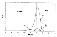
上記の基板の例として、AlN/SiO2/Al/Y−X LiNbO3構造の基板の変位分布を図3に示す。図で、各膜厚は、H2/λ=0.05、H4/λ=0.8、H5/λ=2.0の場合であり、電気機械結合係数k2=0.10,周波数温度特性(TCF)=7ppm/℃の特性が得られる。また、基板上の電極部分、及び薄膜部分にエネルギーが集中していることが判る。
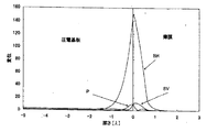
図4は、AlN/SiO2/Cu/128°Y−X LiNbO3構造の基板の変位分布を示す。図で、H2、H3/λ=0.05、H4/λ=1.0、H5/λ=2.0の場合であり、k2=0.055,周波数温度特性(TCF)=22ppm/℃の特性が得られる。図から、基板上の電極部分、及び薄膜部分にエネルギーが集中していることが判る。
図5は、AlN/SiO2/Cu/36°Y−X LiTaO3構造の基板の変位分布である。図で、H2、H3/λ=0.05、H4/λ=0.6、H5/λ=1.5〜2.0の場合であり、k2=0.056,周波数温度特性(TCF)=−0ppm/℃の特性が得られる。図から、基板上の電極部分、及び薄膜部分にエネルギーが集中していることが判る。
図6は、AlN/SiO2/Al、Cu,Ag,Au/Y−X LiNbO3基板の弾性境界波の存在領域を示す図であり、Au、Ag、Cu、Al電極をパラメーターとして、横軸が電極膜厚H2/λ、H3/λ、縦軸がSiO2薄膜H4/λであり、AlN膜厚H5/λ=1.0〜2.0とした場合の存在領域を示す曲線であり、図の矢印の方向が弾性境界波が存在する領域である。例として、Al電極の場合は、H2/λ=0.05では、SiO2膜厚H4/λ=0.45以上で弾性境界波領域が存在することを示す。
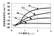
図7は、AlN/SiO2/電極/Y−XLiNbO3基板の電極膜厚H2、H3/λ=0.05の場合の種々の金属に対する、薄膜5としてH5/λ=1.0〜2.0のAlN薄膜とした場合のSiO2薄膜の膜厚H4/λに対する周波数温度特性(TCF)を示す。図からAuでは、零周波数温度特性は得られないこと、また、Cu電極では、SiO2膜H4/λ=1.2で零周波数温度特性が得られることが判る。上記の結果は、電極膜として、Al,Cu,Ag,Au、誘電体膜として、SiO2、AlN膜を取り上げて得た結果であるが、薄膜5の横波速度が薄膜4より早い横波速度の場合は同様の境界波が得られるので本特許に含まれる。
以上の例では、最上部の薄膜AlNの膜厚H5/λ=1.0〜2.0と十分に厚いとした場合の境界波について解析を行ったが、実用のデバイスでは、境界波となる最上部の膜厚が出来るだけ薄い場合のデバイスが必要であり、請求項7の最上部の膜厚として示した範囲、即ちH5/λ=0.005〜3.5の範囲での境界波の存在する最小膜厚の解析結果及び実験結果を示す。
図8は、AlN/SiO2/Al/Y−X LiNbO3基板でHAl/λ=0.05の場合のAlN膜厚に対する伝搬速度の変化を示したもので、SiO2膜厚HSiO2/λ=0.4付近以下では、AlN膜厚の変化に対する伝搬速度の変化が一定となる領域が遅い横波より小さい領域では存在しないので境界波が存在しないこと、またSiO2膜厚HSiO2/λ=0.5以上の場合、膜厚HAlN/λ=0.5以上では、AlN膜厚の変化に対する伝搬速度の変化はほぼ一定となる領域が存在するので、境界波が存在すること、また、0.5以上のAlN膜は、不要であること、かつ最上部に厚い膜を付着させることは、境界波基板の割れ、
![]()
図9は、AlN/SiO2/Cu/Y−X LiNbO3基板でHCu/λ=0.04の場合のAlN膜厚に対する伝搬速度の変化を示したもので、SiO2膜厚HSiO2/λ=0.15付近以下では、境界波が存在しないこと、またSiO2膜厚HSiO2/λ=0.2以上の場合、膜厚HAlN/λ=0.4以上では、殆どHCu/λに対する伝搬速度の変化は無くなり、境界波となるので、0.4以上のAlN膜は、不要であること、かつ厚い膜を付着させることは、境界波基板の割れ、最上部膜の亀裂、剥離を伴うので基板の悪影響を与える結果となるので、出来るだけ薄いH/λとして、0.4とすることで、最適の基板が得られる。
図10は、AlN/SiO2/Cu/10°Y−X LiNbO3基板でHCu/λ=0.03の場合のAlN膜厚に対する伝搬速度の変化を示したもので、SiO2膜厚HSiO2/λ=0.25付近以下では、境界波が存在しないこと、またSiO2膜厚HSiO2/λ=0.35付近以上の場合、膜厚HAlN/λ=0.45以上では、膜厚HAlN/λの変化に対する伝搬速度の変化は殆ど無くなり、境界波となるので、0.5以上のAlN膜は、不要であること、かつ厚い膜を付着させることは、境界波基板の割れ、最上部膜の亀裂、剥離を伴うので基板の悪影響を与える結果となるので、出来るだけ薄いH/λとして、0.5とすることで、最適の基板が得られる。。
図11は、境界波を得るためのSiO2膜厚に対する最上部AlN膜の最小値をHCu/λ(図では、Cu=0.1はHCu/λ=0.1に対応する)をパラメーターとした、AlN/SiO2/Cu/Y−X LiNbO3基板について、境界波の得られる条件して、プロット条件に示すような条件、即ち、AlN膜の変化(Hi/λ−Hi+1/λ)に対する速度の変化(vi+1−vi)/viの値が10−3した場合の境界波が得られるAlNとSiO2最小膜厚の関係を示した図であり、境界波はこの曲線より上の領域で存在することを示している。例えば、SiO2膜厚HSiO2/λ=0.5では、HCu/λCu=0.05の場合、HAlN/λ=0.45以上が境界波の存在範囲となることを示す。
図12は、境界波を得るためのSiO2膜厚に対する最上部AlN膜の最小値をHCu/λ(図では、Cu=0.3はHCu/λ=0.0375に対応する)をパラメーターとした、AlN/SiO2/Cu/36°Y−X LiTaO3基板について、境界波の得られる条件して、プロット条件に示すような条件、即ち、AlN膜の変化(Hi/λ−Hi+1/λ)に対する速度の変化(vi+1−vi)/viの値が10−3した場合の境界波が得られるAlNとSiO2最小膜厚の関係を示した図であり、境界波はこの曲線より上の領域で存在することを示している。例えば、SiO2膜厚HSiO2/λ=0.4では、HCu/λCu=0.0375の場合、HAlN/λ=0.5以上が境界波の存在範囲となることを示す。
図13は、AlN/SiO2/Cu電極/Y−XLiNbO3基板を用いた共振器の実験結果であり、電極3として、H3/λ=0.04のCu、薄膜4としてH4/λ=0.225のSiO2を付着させた上に薄膜5として、AlN薄膜を付着させ、その膜厚H5/λを大きくして行った場合の共振中心周波数の変化であり、H5/λ=0.5以上では、殆ど中心周波数は変化せず、AlN表面の変位は殆ど零であり、弾性境界波になっていることが判る。
図14は、図13に示した弾性境界波共振器のアドミッタンスの周波数特性である。
図から良好な共振特性が得られていることが判る。また、AlN表面に伝搬減衰の大きなレジストを付着させても特性変化はなかった。
図15は、AlN/SiO2/Cu電極/36°Y−X LiTaO3基板を用いた共振器の実験結果であり、電極3として、H3/λ=0.037のCu、薄膜4としてH4/λ=0.25のSiO2を付着させた上に薄膜5として、AlN薄膜を付着させ、その膜厚H5/λを大きくして行った場合のアドミッタンスの周波数特性であり、HAlN/λ=0.78(AlN=6.3μm)の基板表面に伝搬損失の大きなホトレジスト膜を3μm付着させない特性と付着させた特性には殆ど変化関係が無かったことから、最上部表面には、殆ど変位のない境界波になっていることが解る。この場合も最上部の膜厚は、HAlN/λ=0.78で十分であることが解る。また、この基板の場合、不要波が殆ど発生していないことから、回転Y−X LiTaO3基板では不要波の無い良好なフィルタ特性を容易に得ることができる。
図16は、TeO2薄膜λ/4グレーティング薄膜反射器を用いた一方向性すだれ状電極フィルタの実験結果であり、基板は、AlN/SiO2/TeO2グレーティング薄膜/Y−X LiNbO3構造であり、AlN膜厚5.6λ、SiO2膜厚0.3λ、Cu電極膜厚0.03λであり、良好な一方向特性と低損失特性が得られている。
図17は、特許請求の範囲10において、回転Y−X伝搬の基板1の上に電極膜2、3、その上に薄膜4より大きな横波速度をもつAlN薄膜22をパラメーターとして、Hhs/λ=0,0.05,0.075,0.1を付着させ、その上にSiO2薄膜をH/λ=0〜2.0まで付着させ、その上にAlN膜をH/λ=1.5を付着させた境界波の周波数温度特性であり、零周波数温度特性の得られるSiO2膜厚が、AlN22が零の場合の半分の値で得られることが判る。
以上は、薄膜4より横波速度の大きな薄膜として、AlNを取り上げて示したが、薄膜4より大きな横波速度をもつ種々の薄膜を用いることにより、同様の結果が得られるので、異なる薄膜の組み合わせも本特許に含まれる。As an example of the above substrate, FIG. 3 shows a displacement distribution of a substrate having an AlN / SiO 2 / Al / Y—X LiNbO 3 structure. In the figure, the respective film thicknesses are the cases of H 2 /λ=0.05, H 4 /λ=0.8, H 5 /λ=2.0, and the electromechanical coupling coefficient k 2 = 0.10, A frequency temperature characteristic (TCF) = 7 ppm / ° C. characteristic is obtained. It can also be seen that energy is concentrated on the electrode portion and the thin film portion on the substrate.
FIG. 4 shows a displacement distribution of a substrate having an AlN / SiO 2 / Cu / 128 ° Y—X LiNbO 3 structure. In the figure, H 2 , H 3 /λ=0.05, H 4 /λ=1.0, H 5 /λ=2.0, k 2 = 0.055, frequency temperature characteristic (TCF) A characteristic of = 22 ppm / ° C. is obtained. From the figure, it can be seen that energy is concentrated on the electrode portion and the thin film portion on the substrate.
FIG. 5 is a displacement distribution of a substrate having an AlN / SiO 2 / Cu / 36 ° YX LiTaO 3 structure. In the figure, H 2 , H 3 /λ=0.05, H 4 /λ=0.6, H 5 /λ=1.5 to 2.0, k 2 = 0.056, frequency temperature The characteristic (TCF) = − 0 ppm / ° C. is obtained. From the figure, it can be seen that energy is concentrated on the electrode portion and the thin film portion on the substrate.
FIG. 6 is a diagram showing the existence region of the boundary acoustic wave of the AlN / SiO 2 / Al, Cu, Ag, Au / Y—X LiNbO 3 substrate, with the Au, Ag, Cu, and Al electrodes as parameters. Are the electrode film thicknesses H 2 / λ, H 3 / λ, the vertical axis is the SiO 2 thin film H 4 / λ, and the AlN film thickness H 5 /λ=1.0 to 2.0 indicates the existing region. It is a curve, and the direction of the arrow in the figure is the region where the boundary acoustic wave exists. As an example, in the case of an Al electrode, when H 2 /λ=0.05, the boundary acoustic wave region is present when the SiO 2 film thickness is H 4 /λ=0.45 or more.
7, AlN / SiO 2 / electrodes / Y-XLiNbO 3 for various metals in the case of a substrate of the
In the above example, the boundary wave in the case where the thickness H 5 /λ=1.0 to 2.0 of the uppermost thin film AlN is sufficiently thick has been analyzed. A device is required where the top film thickness is as thin as possible, and the boundary in the range shown as the top film thickness in
FIG. 8 shows a change in propagation speed with respect to the AlN film thickness when the AlN / SiO 2 / Al / YX LiNbO 3 substrate is H Al /λ=0.05, and the SiO 2 film thickness H SiO2 / lambda = 0.4 around less, since the region where the change in propagation speed against the change of the AlN film thickness is constant is not present in the smaller area than the slow shear wave that boundary wave is not present, also SiO 2 film thickness H SiO2 / lambda = 0.5 or more In the case of film thickness H AlN /λ=0.5 or more, there is a region where the change in propagation velocity with respect to the change in AlN film thickness is almost constant, so that there is a boundary wave, , An AlN film of 0.5 or more is not necessary, and attaching a thick film on the top is a crack of the boundary wave substrate,
![]()
FIG. 9 shows the change in the propagation speed with respect to the AlN film thickness in the case of H Cu /λ=0.04 in the AlN / SiO 2 / Cu / YX LiNbO 3 substrate, and shows the SiO 2 film thickness H SiO2 / lambda = 0.15 around less, it does not exist a boundary wave, and if the SiO 2 film thickness H SiO2 /λ=0.2 above, the thickness H AlN /λ=0.4 above, most H Cu / Since the change of the propagation velocity with respect to λ is eliminated and a boundary wave is generated, an AlN film of 0.4 or more is not necessary, and attaching a thick film causes a crack in the boundary wave substrate, a crack in the uppermost film, Since peeling is accompanied by a negative effect on the substrate, an optimum substrate can be obtained by setting H / λ as thin as possible to 0.4.
Figure 10 is intended in AlN / SiO 2 / Cu / 10
FIG. 11 shows the minimum value of the uppermost AlN film with respect to the SiO 2 film thickness for obtaining the boundary wave as H Cu / λ (in the figure, Cu = 0.1 corresponds to H Cu /λ=0.1). For the AlN / SiO 2 / Cu / YX LiNbO 3 substrate as a parameter, the conditions for obtaining the boundary wave are the conditions shown in the plot conditions, that is, the change of the AlN film (H i / λ−H i + 1 / lambda) change in velocity with respect to (v i + 1 -v i) / v is a diagram values showed 10 -3 relationship of AlN and SiO 2 minimum film thickness boundary wave is obtained in the case of i, the boundary wave It shows that it exists in the region above this curve. For example, the SiO 2 film thickness H SiO2 /λ=0.5, when the H Cu /λCu=0.05, indicating that H AlN /λ=0.45 or the existence range of the boundary wave.
FIG. 12 shows the minimum value of the uppermost AlN film with respect to the SiO 2 film thickness for obtaining the boundary wave as H Cu / λ (in the figure, Cu = 0.3 corresponds to H Cu /λ=0.0375). With respect to the AlN / SiO 2 / Cu / 36 ° YX LiTaO 3 substrate as a parameter, the conditions shown in the plot conditions, that is, the change of the AlN film (H i / λ− H i + 1 / λ) change in velocity with respect to (v i + 1 -v i) / v is a diagram values showed 10 -3 relationship of AlN and SiO 2 minimum film thickness boundary wave is obtained in the case of i, the boundary Waves are present in the region above this curve. For example, the SiO 2 film thickness H SiO2 /λ=0.4, when the H Cu / λ Cu = 0.0375, indicating that H AlN /λ=0.5 or the existence range of the boundary wave.
FIG. 13 shows the experimental results of a resonator using an AlN / SiO 2 / Cu electrode / Y-XLiNbO 3 substrate. As an
FIG. 14 shows frequency characteristics of admittance of the boundary acoustic wave resonator shown in FIG.
It can be seen from the figure that good resonance characteristics are obtained. Further, there was no change in characteristics even when a resist with large propagation attenuation was attached to the AlN surface.
FIG. 15 shows the experimental results of the resonator using the AlN / SiO 2 / Cu electrode / 36 ° YX LiTaO 3 substrate. As the
FIG. 16 shows the experimental results of a unidirectional interdigital transducer using a TeO 2 thin film λ / 4 grating thin film reflector. The substrate has an AlN / SiO 2 / TeO 2 grating thin film / YX LiNbO 3 structure. In other words, the AlN film thickness is 5.6λ, the SiO 2 film thickness is 0.3λ, and the Cu electrode film thickness is 0.03λ. Good unidirectional characteristics and low loss characteristics are obtained.
17, in the
The above shows AlN as a thin film having a greater transverse wave velocity than the
1−圧電性基板、2−金属薄膜、3−すだれ状電極、4−誘電体薄膜、5−誘電体薄膜或いは金属薄膜、1-piezoelectric substrate, 2-metal thin film, 3-interdigital electrode, 4-dielectric thin film, 5-dielectric thin film or metal thin film,
Claims (4)
前記LiNbO3基板に付着されたAl電極膜と、
前記Al電極膜に付着されたSiO2膜と、
前記SiO2膜に付着されたAlN膜とを備え、
境界波の中心周波数での波長をλとして、
前記Al電極膜の膜厚H2/λ或はH 3 /λの値は、0.05以上であり、
前記SiO2膜の膜厚H4/λの値は、0.5以上であり、
前記AlN膜の膜厚H5/λの値は、0.5以上であり、
前記LiNbO 3 基板の厚さ方向のエネルギー放射量が0より大きくかつ全体のエネルギーの1/8以下であり、前記AlN膜の上面におけるエネルギー量が0より大きくかつ全体のエネルギーの1/8以下である弾性境界波機能素子。 -10 ° -90 ° rotated Y-cut X-propagation LiNbO 3 substrate;
An Al electrode film attached to the LiNbO 3 substrate;
A SiO 2 film attached to the Al electrode film;
An AlN film attached to the SiO 2 film;
Assuming that the wavelength at the center frequency of the boundary wave is λ,
The film thickness H 2 / λ or H 3 / λ of the Al electrode film is 0.05 or more,
The thickness H 4 / λ of the SiO 2 film is 0.5 or more,
The thickness H 5 / λ of the AlN film is 0.5 or more ,
The energy radiation amount in the thickness direction of the LiNbO 3 substrate is greater than 0 and 1/8 or less of the total energy, and the energy amount on the upper surface of the AlN film is greater than 0 and 1/8 or less of the total energy. A boundary acoustic wave functional element.
前記LiNbO3基板に付着されたCu電極膜と、
前記Cu電極膜に付着されたSiO2膜と、
前記SiO2膜に付着されたAlN膜とを備え、
境界波の中心周波数での波長をλとして、
前記Cu電極膜の膜厚H2/λ或はH 3 /λの値は、0.04以上であり、
前記SiO2膜の膜厚H4/λの値は、0.2以上であり、
前記AlN膜の膜厚H5/λの値は、0.4以上であり、
前記LiNbO 3 基板の厚さ方向のエネルギー放射量が0より大きくかつ全体のエネルギーの1/8以下であり、前記AlN膜の上面におけるエネルギー量が0より大きくかつ全体のエネルギーの1/8以下である弾性境界波機能素子。 -10 ° -90 ° rotated Y-cut X-propagation LiNbO 3 substrate;
A Cu electrode film attached to the LiNbO 3 substrate;
A SiO 2 film attached to the Cu electrode film;
An AlN film attached to the SiO 2 film;
Assuming that the wavelength at the center frequency of the boundary wave is λ,
The value of the film thickness H 2 / λ or H 3 / λ of the Cu electrode film is 0.04 or more,
The thickness H 4 / λ of the SiO 2 film is 0.2 or more,
The film thickness H 5 / λ of the AlN film is 0.4 or more ,
The energy radiation amount in the thickness direction of the LiNbO 3 substrate is greater than 0 and 1/8 or less of the total energy, and the energy amount on the upper surface of the AlN film is greater than 0 and 1/8 or less of the total energy. A boundary acoustic wave functional element.
前記LiNbO3基板に付着されたCu電極膜と、
前記Cu電極膜に付着されたSiO2膜と、
前記SiO2膜に付着されたAlN膜とを備え、
境界波の中心周波数での波長をλとして、
前記Cu電極膜の膜厚H2/λ或はH 3 /λの値は、0.03以上であり、
前記SiO2膜の膜厚H4/λの値は、0.35以上であり、
前記AlN膜の膜厚H5/λの値は、0.5以上であり、
前記LiNbO 3 基板の厚さ方向のエネルギー放射量が0より大きくかつ全体のエネルギーの1/8以下であり、前記AlN膜の上面におけるエネルギー量が0より大きくかつ全体のエネルギーの1/8以下である弾性境界波機能素子。 A −10 ° to 90 ° LiNbO 3 substrate,
A Cu electrode film attached to the LiNbO 3 substrate;
A SiO 2 film attached to the Cu electrode film;
An AlN film attached to the SiO 2 film;
Assuming that the wavelength at the center frequency of the boundary wave is λ,
The value of the film thickness H 2 / λ or H 3 / λ of the Cu electrode film is 0.03 or more,
The thickness H 4 / λ of the SiO 2 film is 0.35 or more,
The thickness H 5 / λ of the AlN film is 0.5 or more ,
The energy radiation amount in the thickness direction of the LiNbO 3 substrate is greater than 0 and 1/8 or less of the total energy, and the energy amount on the upper surface of the AlN film is greater than 0 and 1/8 or less of the total energy. A boundary acoustic wave functional element.
Priority Applications (3)
| Application Number | Priority Date | Filing Date | Title |
|---|---|---|---|
| JP2008098723A JP5154285B2 (en) | 2007-05-28 | 2008-03-09 | Boundary acoustic wave functional element |
| US12/601,687 US8508101B2 (en) | 2007-05-28 | 2008-05-28 | Elastic boundary wave substrate and elastic boundary wave functional element using the substrate |
| PCT/JP2008/001329 WO2008146489A1 (en) | 2007-05-28 | 2008-05-28 | Elastic boundary wave substrate and elastic boundary wave functional element using the substrate |
Applications Claiming Priority (3)
| Application Number | Priority Date | Filing Date | Title |
|---|---|---|---|
| JP2007166939 | 2007-05-28 | ||
| JP2007166939 | 2007-05-28 | ||
| JP2008098723A JP5154285B2 (en) | 2007-05-28 | 2008-03-09 | Boundary acoustic wave functional element |
Publications (3)
| Publication Number | Publication Date |
|---|---|
| JP2009010927A JP2009010927A (en) | 2009-01-15 |
| JP2009010927A5 JP2009010927A5 (en) | 2011-04-21 |
| JP5154285B2 true JP5154285B2 (en) | 2013-02-27 |
Family
ID=40325493
Family Applications (1)
| Application Number | Title | Priority Date | Filing Date |
|---|---|---|---|
| JP2008098723A Active JP5154285B2 (en) | 2007-05-28 | 2008-03-09 | Boundary acoustic wave functional element |
Country Status (2)
| Country | Link |
|---|---|
| US (1) | US8508101B2 (en) |
| JP (1) | JP5154285B2 (en) |
Families Citing this family (8)
| Publication number | Priority date | Publication date | Assignee | Title |
|---|---|---|---|---|
| JP2009088730A (en) * | 2007-09-28 | 2009-04-23 | Samsung Electronics Co Ltd | Elastic boundary wave device |
| CN102017407B (en) | 2008-04-30 | 2014-03-19 | 株式会社村田制作所 | Elastic boundary wave device |
| JPWO2010116783A1 (en) * | 2009-03-30 | 2012-10-18 | 株式会社村田製作所 | Elastic wave device |
| WO2010122993A1 (en) * | 2009-04-22 | 2010-10-28 | 株式会社村田製作所 | Elastic boundary wave device and manufacturing method therefor |
| JP2011041127A (en) * | 2009-08-17 | 2011-02-24 | Hitachi Media Electoronics Co Ltd | Elastic wave device |
| DE102011119660B4 (en) * | 2011-11-29 | 2014-12-11 | Epcos Ag | Microacoustic device with waveguide layer |
| US11673352B2 (en) * | 2016-09-20 | 2023-06-13 | United States Of America As Represented By The Administrator Of Nasa | Automated wave guide system for in-process monitoring of carbon fiber reinforced polymer (CFRP) composite laminates with hanning window tone-bursts of center frequencies from 100-225 kHz and 100-350 kHz |
| GB2569082A (en) * | 2016-10-20 | 2019-06-05 | Skyworks Solutions Inc | Elastic wave device with sub-wavelength thick piezoelectric layer |
Family Cites Families (11)
| Publication number | Priority date | Publication date | Assignee | Title |
|---|---|---|---|---|
| US5111100A (en) * | 1990-01-12 | 1992-05-05 | Clarion Co., Ltd. | Surface acoustic wave device and method for fabricating same |
| EP0903851A4 (en) * | 1996-06-05 | 2001-02-14 | Sanyo Electric Co | Surface acoustic wave element |
| WO1998052279A1 (en) * | 1997-05-12 | 1998-11-19 | Hitachi, Ltd. | Elastic wave device |
| US7105980B2 (en) * | 2002-07-03 | 2006-09-12 | Sawtek, Inc. | Saw filter device and method employing normal temperature bonding for producing desirable filter production and performance characteristics |
| JP3815424B2 (en) * | 2002-11-08 | 2006-08-30 | 株式会社村田製作所 | Boundary acoustic wave device |
| CN1788415B (en) * | 2004-01-19 | 2012-09-12 | 株式会社村田制作所 | Acoustic boundary wave device |
| EP1732214A4 (en) * | 2004-03-29 | 2008-08-06 | Murata Manufacturing Co | Boundary acoustic wave device manufacturing method and boundary acoustic wave device |
| CN1829082B (en) * | 2005-03-04 | 2010-05-26 | 鸿富锦精密工业(深圳)有限公司 | Surface acoustic wave device and multi-frequency mobile phone |
| JP2006279609A (en) * | 2005-03-29 | 2006-10-12 | Fujitsu Media Device Kk | Elastic boundary wave element, resonator, and ladder filter |
| EP1879291A4 (en) * | 2005-04-25 | 2012-02-22 | Murata Manufacturing Co | Boundary acoustic wave device |
| US7446453B1 (en) * | 2006-07-05 | 2008-11-04 | Triquint, Inc. | Surface acoustic wave devices using surface acoustic waves with strong piezoelectric coupling |
-
2008
- 2008-03-09 JP JP2008098723A patent/JP5154285B2/en active Active
- 2008-05-28 US US12/601,687 patent/US8508101B2/en active Active
Also Published As
| Publication number | Publication date |
|---|---|
| US8508101B2 (en) | 2013-08-13 |
| US20100171389A1 (en) | 2010-07-08 |
| JP2009010927A (en) | 2009-01-15 |
Similar Documents
| Publication | Publication Date | Title |
|---|---|---|
| JP7051690B2 (en) | Induced surface acoustic wave device that results in spurious mode removal | |
| JP5154285B2 (en) | Boundary acoustic wave functional element | |
| JP4757860B2 (en) | Surface acoustic wave functional element | |
| US7489065B2 (en) | Boundary acoustic wave device | |
| JP5099151B2 (en) | Method for manufacturing boundary acoustic wave device | |
| US7323803B2 (en) | Boundary acoustic wave device | |
| JP6736006B2 (en) | Acoustic wave device and method for manufacturing the same | |
| KR20190077224A (en) | Elastic wave device | |
| JP4760911B2 (en) | Boundary acoustic wave device | |
| WO2004070946A1 (en) | Elastic boundary wave device | |
| WO2006114930A1 (en) | Boundary acoustic wave device | |
| JP4109877B2 (en) | Surface acoustic wave functional element | |
| JPWO2005060094A1 (en) | Boundary acoustic wave device | |
| JPS5861686A (en) | Surface elastic wave element | |
| JP2009010927A5 (en) | ||
| US8198781B2 (en) | Boundary acoustic wave device | |
| JP4001157B2 (en) | Boundary acoustic wave device | |
| JP2008092610A (en) | Surface acoustic wave substrate and surface acoustic wave functional element | |
| JP2012169760A (en) | Surface acoustic wave device | |
| JP4003434B2 (en) | Surface wave device | |
| JP3963081B2 (en) | Surface wave device | |
| JP2014176076A (en) | Surface acoustic wave substrate using surface acoustic wave/pseudo surface acoustic wave/boundary acoustic wave, and surface acoustic wave function element employing the substrate | |
| JP2004282515A (en) | Surface acoustic wave element |
Legal Events
| Date | Code | Title | Description |
|---|---|---|---|
| A711 | Notification of change in applicant |
Free format text: JAPANESE INTERMEDIATE CODE: A711 Effective date: 20081128 |
|
| RD03 | Notification of appointment of power of attorney |
Free format text: JAPANESE INTERMEDIATE CODE: A7423 Effective date: 20081128 |
|
| A521 | Request for written amendment filed |
Free format text: JAPANESE INTERMEDIATE CODE: A821 Effective date: 20081128 |
|
| A521 | Request for written amendment filed |
Free format text: JAPANESE INTERMEDIATE CODE: A523 Effective date: 20110307 |
|
| A621 | Written request for application examination |
Free format text: JAPANESE INTERMEDIATE CODE: A621 Effective date: 20110307 |
|
| A131 | Notification of reasons for refusal |
Free format text: JAPANESE INTERMEDIATE CODE: A131 Effective date: 20120717 |
|
| A521 | Request for written amendment filed |
Free format text: JAPANESE INTERMEDIATE CODE: A523 Effective date: 20120913 |
|
| TRDD | Decision of grant or rejection written | ||
| A01 | Written decision to grant a patent or to grant a registration (utility model) |
Free format text: JAPANESE INTERMEDIATE CODE: A01 Effective date: 20121106 |
|
| A61 | First payment of annual fees (during grant procedure) |
Free format text: JAPANESE INTERMEDIATE CODE: A61 Effective date: 20121205 |
|
| FPAY | Renewal fee payment (event date is renewal date of database) |
Free format text: PAYMENT UNTIL: 20151214 Year of fee payment: 3 |
|
| R150 | Certificate of patent or registration of utility model |
Ref document number: 5154285 Country of ref document: JP Free format text: JAPANESE INTERMEDIATE CODE: R150 Free format text: JAPANESE INTERMEDIATE CODE: R150 |
|
| S111 | Request for change of ownership or part of ownership |
Free format text: JAPANESE INTERMEDIATE CODE: R313115 |
|
| R360 | Written notification for declining of transfer of rights |
Free format text: JAPANESE INTERMEDIATE CODE: R360 |
|
| R370 | Written measure of declining of transfer procedure |
Free format text: JAPANESE INTERMEDIATE CODE: R370 |
|
| S111 | Request for change of ownership or part of ownership |
Free format text: JAPANESE INTERMEDIATE CODE: R313115 |
|
| R350 | Written notification of registration of transfer |
Free format text: JAPANESE INTERMEDIATE CODE: R350 |
|
| R250 | Receipt of annual fees |
Free format text: JAPANESE INTERMEDIATE CODE: R250 |
|
| S533 | Written request for registration of change of name |
Free format text: JAPANESE INTERMEDIATE CODE: R313533 |
|
| R250 | Receipt of annual fees |
Free format text: JAPANESE INTERMEDIATE CODE: R250 |
|
| R350 | Written notification of registration of transfer |
Free format text: JAPANESE INTERMEDIATE CODE: R350 |
|
| R250 | Receipt of annual fees |
Free format text: JAPANESE INTERMEDIATE CODE: R250 |
|
| R250 | Receipt of annual fees |
Free format text: JAPANESE INTERMEDIATE CODE: R250 |
|
| R250 | Receipt of annual fees |
Free format text: JAPANESE INTERMEDIATE CODE: R250 |
|
| R250 | Receipt of annual fees |
Free format text: JAPANESE INTERMEDIATE CODE: R250 |
|
| R250 | Receipt of annual fees |
Free format text: JAPANESE INTERMEDIATE CODE: R250 |
|
| R250 | Receipt of annual fees |
Free format text: JAPANESE INTERMEDIATE CODE: R250 |
|
| R250 | Receipt of annual fees |
Free format text: JAPANESE INTERMEDIATE CODE: R250 |