EP2374130B1 - Magnetic random access memory with dual spin torque reference layers - Google Patents
Magnetic random access memory with dual spin torque reference layers Download PDFInfo
- Publication number
- EP2374130B1 EP2374130B1 EP09775420.4A EP09775420A EP2374130B1 EP 2374130 B1 EP2374130 B1 EP 2374130B1 EP 09775420 A EP09775420 A EP 09775420A EP 2374130 B1 EP2374130 B1 EP 2374130B1
- Authority
- EP
- European Patent Office
- Prior art keywords
- magnetic
- magnetic layer
- layer
- free
- cell
- Prior art date
- Legal status (The legal status is an assumption and is not a legal conclusion. Google has not performed a legal analysis and makes no representation as to the accuracy of the status listed.)
- Not-in-force
Links
- 230000005291 magnetic effect Effects 0.000 title claims description 377
- 230000009977 dual effect Effects 0.000 title description 10
- 239000010410 layer Substances 0.000 claims description 335
- 230000005415 magnetization Effects 0.000 claims description 156
- 239000011229 interlayer Substances 0.000 claims description 14
- 230000004888 barrier function Effects 0.000 claims description 7
- XEEYBQQBJWHFJM-UHFFFAOYSA-N Iron Chemical compound [Fe] XEEYBQQBJWHFJM-UHFFFAOYSA-N 0.000 claims description 6
- PXHVJJICTQNCMI-UHFFFAOYSA-N Nickel Chemical compound [Ni] PXHVJJICTQNCMI-UHFFFAOYSA-N 0.000 claims description 6
- 229910052782 aluminium Inorganic materials 0.000 claims description 5
- XAGFODPZIPBFFR-UHFFFAOYSA-N aluminium Chemical compound [Al] XAGFODPZIPBFFR-UHFFFAOYSA-N 0.000 claims description 5
- 239000003302 ferromagnetic material Substances 0.000 claims description 5
- RYGMFSIKBFXOCR-UHFFFAOYSA-N Copper Chemical compound [Cu] RYGMFSIKBFXOCR-UHFFFAOYSA-N 0.000 claims description 4
- 229910052802 copper Inorganic materials 0.000 claims description 4
- 239000010949 copper Substances 0.000 claims description 4
- 229910017052 cobalt Inorganic materials 0.000 claims description 3
- 239000010941 cobalt Substances 0.000 claims description 3
- GUTLYIVDDKVIGB-UHFFFAOYSA-N cobalt atom Chemical compound [Co] GUTLYIVDDKVIGB-UHFFFAOYSA-N 0.000 claims description 3
- 229910001291 heusler alloy Inorganic materials 0.000 claims description 3
- 229910052742 iron Inorganic materials 0.000 claims description 3
- 229910052759 nickel Inorganic materials 0.000 claims description 3
- ZOXJGFHDIHLPTG-UHFFFAOYSA-N Boron Chemical compound [B] ZOXJGFHDIHLPTG-UHFFFAOYSA-N 0.000 claims description 2
- FYYHWMGAXLPEAU-UHFFFAOYSA-N Magnesium Chemical compound [Mg] FYYHWMGAXLPEAU-UHFFFAOYSA-N 0.000 claims description 2
- BQCADISMDOOEFD-UHFFFAOYSA-N Silver Chemical compound [Ag] BQCADISMDOOEFD-UHFFFAOYSA-N 0.000 claims description 2
- RTAQQCXQSZGOHL-UHFFFAOYSA-N Titanium Chemical compound [Ti] RTAQQCXQSZGOHL-UHFFFAOYSA-N 0.000 claims description 2
- 229910052796 boron Inorganic materials 0.000 claims description 2
- 239000004020 conductor Substances 0.000 claims description 2
- PCHJSUWPFVWCPO-UHFFFAOYSA-N gold Chemical compound [Au] PCHJSUWPFVWCPO-UHFFFAOYSA-N 0.000 claims description 2
- 229910052737 gold Inorganic materials 0.000 claims description 2
- 239000010931 gold Substances 0.000 claims description 2
- 229910052749 magnesium Inorganic materials 0.000 claims description 2
- 239000011777 magnesium Substances 0.000 claims description 2
- 229910000889 permalloy Inorganic materials 0.000 claims description 2
- 229910052709 silver Inorganic materials 0.000 claims description 2
- 239000004332 silver Substances 0.000 claims description 2
- 229910052715 tantalum Inorganic materials 0.000 claims description 2
- GUVRBAGPIYLISA-UHFFFAOYSA-N tantalum atom Chemical compound [Ta] GUVRBAGPIYLISA-UHFFFAOYSA-N 0.000 claims description 2
- 239000010936 titanium Substances 0.000 claims description 2
- 229910052719 titanium Inorganic materials 0.000 claims description 2
- 229910052779 Neodymium Inorganic materials 0.000 claims 1
- 229910052772 Samarium Inorganic materials 0.000 claims 1
- 229910052747 lanthanoid Inorganic materials 0.000 claims 1
- 150000002602 lanthanoids Chemical class 0.000 claims 1
- QEFYFXOXNSNQGX-UHFFFAOYSA-N neodymium atom Chemical compound [Nd] QEFYFXOXNSNQGX-UHFFFAOYSA-N 0.000 claims 1
- KZUNJOHGWZRPMI-UHFFFAOYSA-N samarium atom Chemical compound [Sm] KZUNJOHGWZRPMI-UHFFFAOYSA-N 0.000 claims 1
- 210000004027 cell Anatomy 0.000 description 104
- 238000013500 data storage Methods 0.000 description 54
- 210000000352 storage cell Anatomy 0.000 description 33
- 238000000034 method Methods 0.000 description 22
- 230000008569 process Effects 0.000 description 13
- 230000000295 complement effect Effects 0.000 description 7
- 238000005516 engineering process Methods 0.000 description 7
- 230000006870 function Effects 0.000 description 7
- 230000008859 change Effects 0.000 description 6
- 230000005641 tunneling Effects 0.000 description 5
- PNEYBMLMFCGWSK-UHFFFAOYSA-N Alumina Chemical compound [O-2].[O-2].[O-2].[Al+3].[Al+3] PNEYBMLMFCGWSK-UHFFFAOYSA-N 0.000 description 4
- 230000008901 benefit Effects 0.000 description 4
- 239000000463 material Substances 0.000 description 4
- 230000000875 corresponding effect Effects 0.000 description 3
- 230000000977 initiatory effect Effects 0.000 description 3
- CPLXHLVBOLITMK-UHFFFAOYSA-N magnesium oxide Inorganic materials [Mg]=O CPLXHLVBOLITMK-UHFFFAOYSA-N 0.000 description 3
- 125000006850 spacer group Chemical group 0.000 description 3
- 230000000052 comparative effect Effects 0.000 description 2
- 238000013461 design Methods 0.000 description 2
- 230000000694 effects Effects 0.000 description 2
- 239000012777 electrically insulating material Substances 0.000 description 2
- 230000005669 field effect Effects 0.000 description 2
- 239000011810 insulating material Substances 0.000 description 2
- 239000000395 magnesium oxide Substances 0.000 description 2
- 229910052751 metal Inorganic materials 0.000 description 2
- 239000002184 metal Substances 0.000 description 2
- 230000004044 response Effects 0.000 description 2
- 239000004065 semiconductor Substances 0.000 description 2
- 238000012546 transfer Methods 0.000 description 2
- VYZAMTAEIAYCRO-UHFFFAOYSA-N Chromium Chemical compound [Cr] VYZAMTAEIAYCRO-UHFFFAOYSA-N 0.000 description 1
- XUIMIQQOPSSXEZ-UHFFFAOYSA-N Silicon Chemical compound [Si] XUIMIQQOPSSXEZ-UHFFFAOYSA-N 0.000 description 1
- ATJFFYVFTNAWJD-UHFFFAOYSA-N Tin Chemical compound [Sn] ATJFFYVFTNAWJD-UHFFFAOYSA-N 0.000 description 1
- 230000009471 action Effects 0.000 description 1
- 229910052787 antimony Inorganic materials 0.000 description 1
- WATWJIUSRGPENY-UHFFFAOYSA-N antimony atom Chemical compound [Sb] WATWJIUSRGPENY-UHFFFAOYSA-N 0.000 description 1
- 229910052785 arsenic Inorganic materials 0.000 description 1
- RQNWIZPPADIBDY-UHFFFAOYSA-N arsenic atom Chemical compound [As] RQNWIZPPADIBDY-UHFFFAOYSA-N 0.000 description 1
- 229910052797 bismuth Inorganic materials 0.000 description 1
- JCXGWMGPZLAOME-UHFFFAOYSA-N bismuth atom Chemical compound [Bi] JCXGWMGPZLAOME-UHFFFAOYSA-N 0.000 description 1
- 229910052804 chromium Inorganic materials 0.000 description 1
- 239000011651 chromium Substances 0.000 description 1
- 238000000576 coating method Methods 0.000 description 1
- 230000002860 competitive effect Effects 0.000 description 1
- 150000001875 compounds Chemical class 0.000 description 1
- 238000001816 cooling Methods 0.000 description 1
- 238000012937 correction Methods 0.000 description 1
- 230000002596 correlated effect Effects 0.000 description 1
- 239000013078 crystal Substances 0.000 description 1
- 238000011161 development Methods 0.000 description 1
- 238000005265 energy consumption Methods 0.000 description 1
- 230000007613 environmental effect Effects 0.000 description 1
- 238000001093 holography Methods 0.000 description 1
- 238000010348 incorporation Methods 0.000 description 1
- 239000012212 insulator Substances 0.000 description 1
- AXZKOIWUVFPNLO-UHFFFAOYSA-N magnesium;oxygen(2-) Chemical compound [O-2].[Mg+2] AXZKOIWUVFPNLO-UHFFFAOYSA-N 0.000 description 1
- 239000000696 magnetic material Substances 0.000 description 1
- WPBNNNQJVZRUHP-UHFFFAOYSA-L manganese(2+);methyl n-[[2-(methoxycarbonylcarbamothioylamino)phenyl]carbamothioyl]carbamate;n-[2-(sulfidocarbothioylamino)ethyl]carbamodithioate Chemical compound [Mn+2].[S-]C(=S)NCCNC([S-])=S.COC(=O)NC(=S)NC1=CC=CC=C1NC(=S)NC(=O)OC WPBNNNQJVZRUHP-UHFFFAOYSA-L 0.000 description 1
- 238000004519 manufacturing process Methods 0.000 description 1
- 229910044991 metal oxide Inorganic materials 0.000 description 1
- 150000004706 metal oxides Chemical class 0.000 description 1
- 239000000203 mixture Substances 0.000 description 1
- 230000035699 permeability Effects 0.000 description 1
- 230000010287 polarization Effects 0.000 description 1
- 230000002035 prolonged effect Effects 0.000 description 1
- 230000001902 propagating effect Effects 0.000 description 1
- 229910052710 silicon Inorganic materials 0.000 description 1
- 239000010703 silicon Substances 0.000 description 1
- 229910052718 tin Inorganic materials 0.000 description 1
- 239000002918 waste heat Substances 0.000 description 1
Images


Classifications
-
- G—PHYSICS
- G11—INFORMATION STORAGE
- G11C—STATIC STORES
- G11C11/00—Digital stores characterised by the use of particular electric or magnetic storage elements; Storage elements therefor
- G11C11/02—Digital stores characterised by the use of particular electric or magnetic storage elements; Storage elements therefor using magnetic elements
- G11C11/16—Digital stores characterised by the use of particular electric or magnetic storage elements; Storage elements therefor using magnetic elements using elements in which the storage effect is based on magnetic spin effect
- G11C11/161—Digital stores characterised by the use of particular electric or magnetic storage elements; Storage elements therefor using magnetic elements using elements in which the storage effect is based on magnetic spin effect details concerning the memory cell structure, e.g. the layers of the ferromagnetic memory cell
-
- G—PHYSICS
- G11—INFORMATION STORAGE
- G11C—STATIC STORES
- G11C11/00—Digital stores characterised by the use of particular electric or magnetic storage elements; Storage elements therefor
- G11C11/02—Digital stores characterised by the use of particular electric or magnetic storage elements; Storage elements therefor using magnetic elements
- G11C11/16—Digital stores characterised by the use of particular electric or magnetic storage elements; Storage elements therefor using magnetic elements using elements in which the storage effect is based on magnetic spin effect
- G11C11/165—Auxiliary circuits
- G11C11/1675—Writing or programming circuits or methods
-
- G—PHYSICS
- G11—INFORMATION STORAGE
- G11C—STATIC STORES
- G11C11/00—Digital stores characterised by the use of particular electric or magnetic storage elements; Storage elements therefor
- G11C11/02—Digital stores characterised by the use of particular electric or magnetic storage elements; Storage elements therefor using magnetic elements
- G11C11/16—Digital stores characterised by the use of particular electric or magnetic storage elements; Storage elements therefor using magnetic elements using elements in which the storage effect is based on magnetic spin effect
- G11C11/165—Auxiliary circuits
- G11C11/1673—Reading or sensing circuits or methods
-
- G—PHYSICS
- G11—INFORMATION STORAGE
- G11C—STATIC STORES
- G11C5/00—Details of stores covered by group G11C11/00
- G11C5/02—Disposition of storage elements, e.g. in the form of a matrix array
-
- H—ELECTRICITY
- H10—SEMICONDUCTOR DEVICES; ELECTRIC SOLID-STATE DEVICES NOT OTHERWISE PROVIDED FOR
- H10B—ELECTRONIC MEMORY DEVICES
- H10B61/00—Magnetic memory devices, e.g. magnetoresistive RAM [MRAM] devices
-
- H—ELECTRICITY
- H10—SEMICONDUCTOR DEVICES; ELECTRIC SOLID-STATE DEVICES NOT OTHERWISE PROVIDED FOR
- H10N—ELECTRIC SOLID-STATE DEVICES NOT OTHERWISE PROVIDED FOR
- H10N50/00—Galvanomagnetic devices
- H10N50/10—Magnetoresistive devices
Definitions
- Magnetic random access memory MRAM
- STRAM spin torque RAM
- a magnetic cell comprising, in sequence, a fixed bottom magnetic layer, a separator layer, a free magnetic layer, a further separator layer and a fixed top magnetic layer.
- the separator layers may both be tunnelling barrier layers, of which one may include aluminium oxide, while the other may include magnesium oxide.
- US 2005/0254286 discloses a magnetic cell comprising, in sequence, a first pinning layer, a first pinned layer, a non-magnetic spacer layer, a free layer, a spin barrier layer, a second pinned layer and a second pinning layer.
- the spacer layer may be conductive, e.g., including copper, or it may be a barrier layer including an insulator, e.g. alumina. Alternatively, the spacer may be a current-confined layer.
- a magnetic data storage cell applicable to spin-torque random access memory (ST-RAM), is disclosed.
- a magnetic cell includes first and second fixed magnetic layers and a free magnetic layer positioned between the fixed magnetic layers.
- the magnetic cell also includes terminals configured for providing a spin-polarized current through the magnetic layers.
- the first fixed magnetic layer has a magnetization direction that is substantially parallel to the easy axis of the free magnetic layer
- the second fixed magnetic layer has a magnetization direction that is substantially orthogonal to the easy axis of the free magnetic layer.
- the dual fixed magnetic layers provide enhanced spin torque in writing to the free magnetic layer, thereby reducing the required current and reducing the feature size of magnetic data storage cells, and increasing the data storage density of magnetic spin torque data storage.
- a magnetic cell according to an embodiment of the present invention is as defined in claim 1.
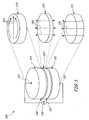
- FIG. 1 depicts a perspective view of a magnetic data storage cell 100, with exploded views of magnetic layers 121, 122, 123 of the cell with illustrated magnetization directions, in accordance with the present invention.
- Many magnetic data storage cells such as magnetic cell 100 may be included together in a data storage device or other data storage system, and configured for storing data, in an illustrative embodiment.
- dual fixed magnetic layers 121, 123 also referred to as reference layers, having complementary magnetization directions, provide enhanced spin torque in writing to the free magnetic layer 122, by switching the magnetization direction of the free magnetic layer 122, as is further described below.
- the enhanced spin torque provided by the dual fixed magnetic layers 121, 123 enables the free magnetic layer 122 to be switched using a lower current, relative to a magnetic cell with just a single fixed magnetic layer.
- This lower current allows reducing the feature size of the magnetic data storage cell 100, relative to a magnetic cell with just a single fixed magnetic layer, and thereby enabling increased data storage density in a magnetic spin torque data storage that incorporates such magnetic data storage cells.
- magnetic cells with a single fixed reference layer may require a larger current than can be provided with integrated field-effect transistors (FET's) typical of integrated circuits, while in contrast, magnetic cells with dual fixed magnetic layers with complementary magnetization directions may function with a lower current that is within the normal current capabilities of an integrated circuit.
- the magnetic layers of cell 100 include a first fixed magnetic layer 121, a second fixed magnetic layer 123, and a free magnetic layer 122 positioned between the first and second fixed magnetic layers 121, 123.
- Magnetic layers 121 and 123 are fixed in that their magnetizations are each kept in a respective fixed direction, while magnetic layer 122 is free in that its magnetization is left free to align in either of two opposing directions along its easy axis, as further explained below.
- Magnetic cell 100 also includes terminals 111, 113 configured for providing a spin-polarized current through the stack of magnetic layers 121, 122, 123. Terminals 111, 113 are connected to node 115 which may connect to additional signal lines (not depicted in FIG.
- the exploded views of the magnetic layers show magnetization direction 141 of fixed magnetic layer 121, indicative of the fixed magnetization direction of magnetic layer 121; magnetization direction 143 of fixed magnetic layer 123, indicative of the fixed magnetization direction of magnetic layer 123; and magnetization direction 142 of free magnetic layer 122, indicative of the easy axis of magnetic layer 122.
- the magnetization of magnetic layer 121 has a perpendicular orientation, also sometimes referred to as out-of-plane or vertical orientation, with the magnetization oriented generally perpendicular to the flat, extended circular surfaces of the layer.
- the magnetization of magnetic layer 123 has a diametrical orientation, also sometimes referred to as in-plane orientation, and oriented generally parallel to the flat surfaces of the layer.
- the magnetization directions 141, 143 of the fixed magnetic layers are each depicted as solid lines, each with an arrowhead on only one end thereof, indicating that the magnetization directions of these magnetic layers are fixed, while the magnetization direction 142 of free magnetic layer is depicted as dashed lines with arrowheads on both ends thereof, indicating that this magnetization direction is indicative of an easy axis, and the magnetization of the layer may be aligned with either polarity of the easy axis with substantially equal stability.
- this will be equal stability, or may be within nominal manufacturing tolerances of equal stability, such that if the magnetization direction of the free magnetic layer is disrupted and allowed to proceed in the absence of environmental influences, the magnetization direction would be equally likely to return to either direction in line with the easy axis.
- the easy axis of the free magnetic layer 122 is set in the perpendicular orientation, in alignment with the magnetization direction 141 of fixed magnetic layer 121, in the illustrative embodiment of FIG. 1 . Therefore, the first fixed magnetic layer 121 has a magnetization direction 141 that is substantially parallel to the easy axis of the free magnetic layer 122, and the second fixed magnetic layer 123 has a magnetization direction 143 that is substantially orthogonal to the easy axis of the free magnetic layer 122, in the illustrative embodiment of FIG. 1 .
- the magnetization direction 142 of the free magnetic layer 122 at any time is predisposed to stable alignment with the easy axis, either parallel or antiparallel to the fixed magnetization direction 141 of magnetic layer 121.
- the magnetization directions are "substantially” parallel and “substantially” orthogonal in a sense that is further discussed below, with reference to FIG. 2 .
- the easy axis may be set by various techniques which may illustratively include shape anisotropy or magnetocrystalline anisotropy in the free magnetic layer.
- the magnetization direction of each of the layers may be kept in a fixed orientation by any of various techniques, such as having the fixed magnetic layers each have a substantially greater magnetic volume than the free magnetic layer, or by having the fixed magnetic layers magnetically pinned, for example.
- the orientation of the magnetization may also be a function of the dimensions of the layer. For example, absent magnetic pinning, a layer having an easy axis (and magnetization) in a diametrical magnetic orientation generally correlates with a relatively larger radius and relatively smaller vertical thickness, while a layer having an easy axis (and magnetization) in a perpendicular magnetic orientation generally correlates with a relatively smaller radius and relatively larger vertical thickness.
- having the perpendicular easy axis for the free magnetic layer 122 may increase the amount of anisotropy energy density of the free layer relative to other easy axis orientations, in this particular embodiment.
- This may enable magnetic cell 100 to have a relatively small size with relatively larger magnetic stability, compared with other orientations.
- a significant constraint on how small magnetic cell 100 can be, while still functioning reliably, is resistance to random reversals of the magnetization direction of free magnetic layer 122 due to random thermal fluctuations.
- the stability of the magnetization direction of the free magnetic layer against thermal disturbances can be modeled as K ⁇ V / kT , where K ⁇ is magnetic anisotropy energy density, V is the volume of the magnetic layer, k is Boltzmann's constant, and T is temperature.
- K ⁇ V / kT K ⁇ V / kT of at least approximately 60 (with no units, because x is a dimensionless ratio) is used as a design standard for maintaining the magnetic stability of the free magnetic layer 122
- the magnetic layers 121, 122, 123 may be composed at least in part of a ferromagnetic material.
- ferromagnetic materials that may be used for the compositions of the magnetic layers include iron, cobalt, nickel, Permalloy, Heusler alloys, or any other ferromagnetic materials.
- Heusler alloys that may be used may, for example, be composed of a combination of two parts of copper, nickel, cobalt, or a combination thereof; one part manganese, chromium, iron, or a combination thereof; and one part tin, aluminum, silicon, arsenic, antimony, bismuth, or boron, or a combination thereof.
- Those skilled in the relevant arts will recognize additional selections of materials that may be well-suited for a given application.
- the intermediate, non-magnetic interlayer 131 is positioned between fixed magnetic layer 121 and free magnetic layer 122, and intermediate, non-magnetic interlayer 132 is positioned between free magnetic layer 122 and fixed magnetic layer 123, in the illustrative embodiment of FIG. 1 .
- Interlayers 131, 132 may be configured to contribute to different technologies for magnetic cell 100, such as quantum tunneling magnetoresistance (TMR) or giant magnetoresistance (GMR), for example.
- TMR quantum tunneling magnetoresistance
- GMR giant magnetoresistance
- One type of interlayer that may be used is a tunnel barrier, configured for quantum tunneling magnetoresistance.
- the tunnel barrier may be composed of an electrically insulating material, such as a metal oxide that may include AlO, TaO, MgO, or any other oxide of aluminum, tantalum, titanium, magnesium, or other appropriate elements or combinations thereof, or other electrically insulating materials.
- an electrically conducting metal layer configured for giant magnetoresistance.
- Such an intermediate layer may be composed of a high-conductance metal such as gold, silver, copper, or aluminum, for example.
- Other types of intermediate layers configured for other purposes, such as interlayers composed of a semiconductor, may be used in various other embodiments.
- first interlayer 131 may be composed of an insulating material for quantum tunneling magnetoresistance
- second interlayer 132 may be composed of a conducing material for giant magnetoresistance.
- first interlayer 131 which separates free magnetic layer 122 from the fixed magnetic layer 121 that has a parallel easy axis and which is used to set the magnetization direction of the free magnetic layer 122, by being composed of an insulating material for quantum tunneling magnetoresistance, may provide for a larger output signal for a read operation.
- second interlayer 132 which separates free magnetic layer 122 from the fixed magnetic layer 123 that has a perpendicular easy axis and which is used for providing the initial torque boost on the magnetization direction of the free magnetic layer 122, by being composed of a conducting material for giant magnetoresistance, could provide for a lower total impedance of the magnetic cell, among other advantages.
- the magnetic cell 100 is thereby enabled to provide dual, complementary spin torques to the free magnetic layer 122, to use a relatively low electric current to store data in magnetic cell 100 in the form of which direction along the easy axis the magnetization direction of free magnetic layer 122 is oriented. How magnetic cell 100 provides these complementary torques and thereby encodes data with relatively low current is further described with reference to FIG. 2 .
- FIG. 2 depicts a side plan view of magnetic data storage cell 100 corresponding to the embodiment depicted in FIG. 1 , with schematic depictions of magnetization directions 141, 142A, 142B, 143, and of spin torques 241, 243 being applied in the cell.
- a spin-polarized current is being passed through magnetic cell 100, with current running from terminal 113 to terminal 111, i.e. with electrons propagating from terminal 111 to terminal 113.
- free magnetic layer 122 initially has magnetization direction 142A, oriented antiparallel to the magnetization direction of fixed magnetic layer 121, i.e. oriented downward as depicted.
- the spin torque 243 gives an initial spin torque boost to magnetization direction 142A to knock it off of the easy axis of free magnetic layer 122 more rapidly and with more initial torque than would be possible with the spin torque 241 from fixed magnetic layer 121 alone; while the spin torque 241 from fixed magnetic layer 121 provides more torque during the middle of the process of reversing the magnetization direction of free magnetic layer 122, and determines the final magnetization direction 142B of free magnetic layer 122 at the end of the write process.
- the current is driven vertically through the stack, between terminals 111 and 113, such that for a positive bias (electron flow from lower terminal 111 to upper terminal 113), spin torque drives the free layer 122 to a final magnetization direction 142B parallel to the magnetization of the fixed layer 121 with the parallel easy axis, as depicted in FIG. 2 .
- spin torque drives the free layer 122 to a final magnetization direction 142A antiparallel to the magnetization direction of the fixed layer 121 with the parallel easy axis (i.e. the opposite of the process depicted in FIG. 2 ).
- each of the two fixed magnetic layers 121, 123 exerts a torque on the magnetization of free magnetic layer 122, and both the rate of change in magnetization 142 of the free magnetic layer 122 and the critical current density must be figured as determined by the equation above with contributions from each of the fixed magnetic layers 121, 123, which drives the rate of change of the magnetization of free magnetic layer 122 much higher, and the critical density much lower, than with a single fixed magnetic layer.
- the magnetization direction of free magnetic layer 122 is depicted in particular orientations labeled 142A and 142B in FIG.
- magnetization direction 142 magnetization 142
- the torque on the magnetization of free magnetic layer 122 is approximately proportional to the cross products of the magnetizations of an adjacent magnetic layer and of the free magnetic layer, i.e. the magnitudes of the magnetizations times the sine of the angle between them. This is illustrated in graph 300 of FIG. 3 .
- FIG. 3 depicts a graphical representation 300 of a superposition of multiple spin torques acting within a cell as a function of angles between magnetization directions, in accordance with an illustrative example.
- torque component 311 represents the magnitude of the spin torque exerted on the magnetization direction of free magnetic layer 122 by fixed magnetic layer 121
- torque component 313 represents the magnitude of the spin torque exerted on the magnetization direction of free magnetic layer 122 by fixed magnetic layer 123.
- the torque associated with magnetization direction 141 of fixed magnetic layer 121 then rises until reaching the full magnitude of the product of the magnetizations 141, 142 of fixed magnetic layer 121 and free magnetic layer 122 respectively, in the middle of a write process, when the magnetization direction of the free magnetic layer 122 is in the middle of flipping and is perpendicular to the magnetization direction 141 of fixed magnetic layer 121.
- the magnetization direction 143 of perpendicular-moment fixed magnetic layer 123 is initially perpendicular to the magnetization direction 142 of free magnetic layer 122.
- the spin angular momentum associated with magnetization direction 143 therefore provides the maximum torque on the magnetization direction 142 of free magnetic layer 122 at the initiation of a write process, i.e. its torque is approximately proportional to 1 (i.e. the sine of 90 degrees) times the product of the magnitudes of magnetizations 142, 143 of free magnetic layer 122 and fixed magnetic layer 123 respectively, at the initiation of the write process.
- the torque from the perpendicular-moment fixed magnetic layer 123 also rises again at the end of the write process, when the torque from the parallel-moment fixed magnetic layer 121 is dropping again.
- the parallel-moment fixed magnetic layer 121 and the perpendicular-moment fixed magnetic layer 123 therefore exert torques that are complementary to each other, and together impose a continuously high torque on the magnetization 142 of free magnetic layer 122 throughout a write process.
- torque components 311 and 313 superpose to form total torque 321, which remains at or above the maximum torque provided by either fixed magnetic layer alone, throughout the write process.
- This provides much faster switching of the magnetization direction 142 of the free magnetic layer 122 than is possible without the dual, complementary fixed magnetic layers of magnetic cell 100. Besides a much lower length of time required for switching, it also enables a much lower level of critical current required for switching.
- the energy required to impose the free layer magnetization switching for a write operation is proportional to the product of the time and the square of the current, and both the time and the current are lower for dual reference layer magnetic cell 100 than with a single reference layer, the energy required for a write operation is also much lower for magnetic cell 100 than for a cell with only one fixed magnetic layer.
- FIG. 4 depicts a comparative graphical representation 400 of magnetoresistance 403 as a function of current 401 for different magnetic cells, in accordance with an illustrative example consistent with the embodiments discussed above.
- Graph 400 further illustrates the benefit of the lower required current as discussed above.
- Graph 400 represents certain relationships between current and magnetoresistance both for dual reference layer magnetic cell 100, and for a hypothetical magnetic cell with only a single fixed magnetic layer and a single free layer, for comparison.
- a magnetic cell with a single free magnetic layer at a point in time may have either a lower magnetoresistance 411 or a higher magnetoresistance 413, where the lower value 411 corresponds to the magnetization direction of the free magnetic layer being parallel to the magnetization direction of the parallel-easy-axis fixed magnetic layer (such as fixed magnetic layer 121 in magnetic cell 100, or which is the only fixed layer in a cell with a single fixed layer), and the higher value 413 corresponds to the magnetization direction of the free magnetic layer being antiparallel to the magnetization direction of the parallel-easy-axis fixed magnetic layer.
- the critical current for switching the magnetization direction of free layer 122 is lower.
- This relatively small critical current for a dual-fixed-layer cell is indicated as I c in FIG. 4 , and is at smaller values of current in both the positive-x and negative-x directions in graph 400.
- Current 421 is depicted for a dual-fixed-layer cell that has been provided the critical current I c and is switching from higher to lower magnetoresistance (or vice-versa on the negative-x side).
- a read operation may be performed on magnetic cell 100 by providing a read query current to magnetic cell 100 with less than the critical current.
- This read query current experiences either the higher level of magnetoresistance 413 or the lower level of magnetoresistance 411 in magnetic cell 100, and returns as a read response voltage equal to the product of the current and resistance that carries the information of what magnetic state the free layer 122 is in at that particular magnetic cell.
- the magnetic cell has the magnetization direction of the free magnetic layer 122 aligned parallel to the magnetization direction of the determining reference layer, i.e.
- the fixed magnetic layer 121 with the magnetization direction parallel to the easy axis of free magnetic layer 122, and a read current of either polarity is provided through the cell, then it experiences a low magnetoresistance, and the output voltage is low.
- the magnetic cell has the magnetization direction of the free magnetic layer 122 aligned antiparallel to the magnetization direction of fixed magnetic layer 121, and a read current is provided through the cell then it experiences a high magnetoresistance, and the output voltage is high, as sensed through the node 115.
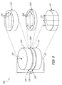
- FIG. 5 depicts a perspective view of a magnetic data storage cell 500, with exploded views of magnetic layers 121, 522, 123 of the cell with magnetization directions 141, 542, 143, in accordance with an example that has some similarities with and some differences from the illustrative embodiment of magnetic cell 100 in FIGS. 1 and 2 , and is not part of the present invention as claimed.
- Magnetic cell 500 has many identical components to magnetic cell 100 of FIGS. 1 and 2 , including fixed magnetic layers 121 and 123, interlayers 131 and 132, terminals 111 and 113, and node 115.
- Magnetic cell 500 also includes free magnetic layer 522, in which the easy axis is oriented in a diametrical orientation, as depicted with magnetization direction 542. The easy axis of free magnetic layer 522 is therefore parallel to the magnetization direction of fixed magnetic layer 123.
- magnetic cell 500 may also exert simultaneous perpendicular spin torques on free magnetic layer 522, i.e. spin torques that are perpendicular to each other and where one of them is perpendicular to the easy axis of free magnetic layer 522 and one spin torque is parallel to the easy axis of free layer 522.
- it is fixed magnetic layer 123 with the magnetization direction that is parallel to the easy axis of free magnetic layer 522 and that provides spin torque that is parallel or antiparallel to the magnetization direction of free layer 522
- fixed magnetic layer 121 has the magnetization direction that is orthogonal to the easy axis of free magnetic layer 522 and that provides spin torque that is orthogonal to the magnetization direction of free layer 522.
- Having the free layer 522 with diametrical easy axis may be advantageous in various illustrative embodiments; for example when the free layer has a relatively high ratio between its radius and its thickness, the diametrical orientation may be more natural and hold its magnetization direction with more stability, in various embodiments.
- FIG. 6 depicts a perspective view of a magnetic data storage cell 600, with exploded views of magnetic layers 621, 522, 123 of the cell with magnetization directions 641, 542, 143, in accordance with another example, in which all three magnetic layers have their magnetization directions and easy axes in diametrical or in-plane orientations, and which likewise does not form part of the invention as claimed.
- many of the components are the same as in magnetic cells 100 and 500 of FIGS. 1 , 2 , and 5 , including fixed magnetic layer 123 as in magnetic cell 100, and free magnetic layer 522 as in magnetic cell 500.
- Magnetic cell 600 also has fixed magnetic layer 621, in which the magnetization is oriented in a second diametrical orientation that is oriented substantially orthogonal to the diametrical orientation of the magnetization of fixed magnetic layer 123 and of the easy axis of free magnetic layer 522. While all the magnetization directions are now in diametrical orientations, the same pattern applies once again in which one of the fixed magnetic layers (123) has its magnetization direction parallel to the easy axis of the free magnetic layer (522), and the other fixed magnetic layer (621) has its magnetization direction orthogonal to the easy axis of the free magnetic layer.
- spin-polarized currents provided through the magnetic cell 600 may be used to switch the magnetization direction of the free magnetic layer 522, where orthogonal-axis fixed magnetic layer 621 acts as the torque booster layer, to complement the determining reference layer to provide the large initial boost of torque to enable a faster switching process with a lower current, while parallel-axis fixed magnetic layer 123 acts as the determining reference layer, providing the torque in the orientation in which the magnetization of free layer 522 will come to rest.
- the embodiment of magnetic cell 600 may provide unique advantages in various embodiments, for example when all the layers have a relatively high ratio of radius to thickness, so that the diametrical orientation may be more natural and may be maintained with higher stability and lower energy or lesser magnetic pinning resources in the case of the fixed magnetic layers 621, 123, as an illustrative example.
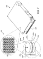
- FIG. 7 depicts a data storage system 700 comprising magnetic data storage cells, in accordance with another illustrative example.
- Data storage system 700 includes a plurality of magnetic data storage cells, such as the illustrative sample 701 of data storage cells 702 shown in a magnified internal view from within data storage system 700.
- the illustrative sample 701 of data storage cells 702 is not represented to scale, and various embodiments of data storage systems may include any number, potentially up through the millions, billions, trillions, or far more, of operably connected dual-reference-layer magnetic data storage cells, like any of magnetic cells 100, 500, 600 discussed above.
- data storage system 700 is depicted as a single device in the illustrative example of FIG.
- other embodiments of data storage systems may include any number of networked or otherwise connected data storage devices, and may include a variety of different types of devices including some comprising compound magnetic data storage cells and others not, distributed over any volume of space. While the array of data storage cells 702 depicted in sample 701 with operable signal lines connected to all the nodes and terminals (like node 115 and terminals 111, 113 in the embodiments discussed above) of the cells 702, this depiction is simplified, and any operable design for sending signals to and receiving signals from the individual magnetic cells may be employed in different embodiments.
- Magnetic data storage cells 702 contained within data storage system 700 include representative magnetic cell 702n, which is depicted in a separate and further magnified view.
- Representative magnetic data storage cell 702n includes first terminal 711n, second terminal 713n, and magnetic cell 702n that includes three substantially cylindrical magnetic layers 721n, 722n, and 723n, along with interlayers 731n, 732n positioned between the adjacent pairs of magnetic layers.
- Magnetic layers 721n and 723n are fixed magnetic layers, while positioned between them is free magnetic layer 722n.
- Magnetic cell 710n and magnetic layers 721n, 722n, and 723n may take the form of any of magnetic cells 100, 500, or 600 of the embodiments discussed above, with their respective magnetic layers, or any other analogous magnetic cell and arrangement of magnetic layers.
- terminal 711n and terminal 713n are configured for providing a spin-polarized current through the magnetic data storage cell 702n.
- Fixed magnetic layer 721n is positioned proximate to the first terminal 711n
- fixed magnetic layer 723n is positioned proximate to the second terminal 713n.
- "Proximate" to a terminal may mean connected to, or at least substantially closer than any of the other layers are, while it may be consistent with additional layers, coatings, sub-terminals, or components within the area around or between the terminals and the magnetic layers, for example.
- Free magnetic layer 722n is positioned between the first and second fixed magnetic layers 721n, 723n.
- one of fixed magnetic layers 721n, 723n has a fixed magnetization direction that is substantially orthogonal to the magnetization direction of the other one of fixed magnetic layers 721n, 723n
- the free magnetic layer 722n has an easy axis that is substantially parallel to a magnetization direction of a parallel-axis determining primary reference layer, the primary reference layer comprising either of fixed magnetic layers 721n, 723n. This predisposes the free magnetic layer 722n to have a magnetization direction either parallel or antiparallel to the magnetization direction of the primary reference layer, in accordance with write operations as discussed above.
- the representative magnetic data storage cell 702n may define a vertical axis that runs generally between the terminals 711n, 713n and generally perpendicular to the magnetic layers 721n, 722n, 723n, in an illustrative embodiment.
- the magnetization direction of the first fixed magnetic layer 721n may be oriented generally parallel to the vertical axis
- the magnetization direction of the second fixed magnetic layer 723n may be oriented either generally parallel or generally orthogonal to the vertical axis
- the easy axis of the free magnetic layer 722n may be oriented generally parallel to the magnetization direction of either the first fixed magnetic layer or the second fixed magnetic layer, in analogy to the various embodiments discussed above with reference to FIGS. 1 , 5 , and 6 , in various illustrative embodiments.
- Data storage system 700 is configured to provide write signals and read signals via the signal connections, whereby the write signals cause spin-polarized currents having a current density above a critical value to be provided through the magnetic data storage cells 702 to controllably set the magnetization direction of the free magnetic layers of the magnetic data storage cells 702, and the read signals cause spin-polarized currents having a current density below the critical value to be provided through the magnetic data storage cells to generate a read output signal that indicates the magnetization direction of the free magnetic layers 722 of the magnetic data storage cells 702.
- the data storage system 700 may store large amounts of data encoded in the magnetization directions of the free magnetic layers of the many magnetic cells 702 of data storage system 700, and may perform read and write operations on the magnetic cells 702 with high speed and low current, as discussed above.
- the current required may be low enough that it is more compatible with integrated semiconductor elements that enable operation of the storage cells, such as field effect transistors (FET's) that are typical components of such a storage device. Additionally, the current required may be low enough that it can be provided by standard integrated circuit current sources, rather than requiring large or bulky devoted current sources to power the magnetic cells.
- the low current also contributes to low rate of energy consumption, low waste heat and a low contribution to system cooling requirements, and prolonged battery life in the case of data storage in a portable device context.
- the fast switching times and high read and write operations contribute to high-speed performance of the data storage system 700.
- FIG. 8 depicts a method 800 associated with one of the magnetic cells discussed above, of using a magnetic cell to write and read data, in accordance with an illustrative example.
- method 800 includes step 803, of providing a free magnetic layer, having first and second sides, the free magnetic layer having an initial magnetization direction aligned with an easy axis; and step 805, of applying a first spin torque at the first side to the free magnetic layer and a second spin torque to the second side of the free magnetic layer, wherein the first spin torque is substantially orthogonal to the initial magnetization direction of the free magnetic layer and the second spin torque is substantially antiparallel to the initial magnetization direction of the free magnetic layer.
- This may serve as a method for writing data to the magnetic cell.
- Method 800 may also include a read process, including step 807, of applying a read current to the free magnetic layer; and step 809, of providing an output based at least in part on a read output signal received in response to the read current.
- a read process including step 807, of applying a read current to the free magnetic layer; and step 809, of providing an output based at least in part on a read output signal received in response to the read current.
- Any kind of data or information may thereby be stored in dual-reference-layer magnetic cells, and the data or information may be retrieved by a read process and used to provide a useful or informative form of tangible output, which may include a display rendered on a monitor, information printed out with a printer, audio data provided to a speaker, a tactile output, or data provided over a hard-wire or wireless signal connection to another computing system, device, router, node, etc. and which may at some point in time be available for incorporation in a user-perceptible output format.
- magnetic layers and magnetic elements are depicted in the figures in a cylindrical form and of identical outer radius, various layers may be used that are of varying radii relative to each other, and of varying morphologies, particularly of morphologies that may be more efficient or may be inherent for the underlying crystal lattices of the materials used, particularly as storage cell size becomes ever smaller in subsequent iterations of development.
- Various embodiments may also use layers in which their magnetization directions or easy axis are bi-stable in any two orientations; or are tri-stable in all three of the orientations mentioned above, including out-of-plane and two orthogonal in-plane orientations; or that are bi-stable or otherwise quasi-stable in diametrical orientations along two or more diametrically oriented axes of the layer.
- Various embodiments may also use other techniques and structures for defining the stable or quasi-stable orientations of the magnetization direction or easy axis of any of the magnetic layers, such as inner cavities defining inner annular radii of the layers, for example.
- embodiments discussed above are discussed in the context of a magnetic cell with a single magnetic free layer
- other embodiments may include a magnetic cell with multiple discrete magnetic free layers, in which a write operation can vary the current and duration of time the current is applied to a cell, in addition to the direction of the current, to controllably switch the magnetic free layers in any combination, thereby writing multiple bits of information to each single magnetic cell, according to an illustrative embodiment.
- the free magnetic layers may have interlayers separating each adjacent pair of free magnetic layers, in an illustrative embodiment, which may define discrete domain walls between adjacent free magnetic layers with opposing magnetization directions.
- Free magnetic layers that have their magnetization directions parallel to the primary, parallel-axis fixed layer may contribute to the spin torque of that parallel-axis fixed layer in switching free layers further down the stack of the magnetic cell, in an illustrative embodiment.
- Magnetic cells with multiple free magnetic layers may provide for relatively larger cells but with more bits stored per cell, and may thereby provide higher overall data storage density, in this illustrative embodiment.
- a data storage cell or data storage system of the present disclosure may be used in association with any technology for the storage and/or manipulation of data, including those involving magnetoresistance, giant magnetoresistance, colossal magnetoresistance, flash memory, optics, magneto-optics, photonics, spintronics, holography, and any other technology.
- Various embodiments may also be incorporated in multi-technology devices that store or otherwise manipulate data with different components using magnetic cells as well as other technologies, such as disc drives or flash drives, for storing or manipulating different portions of data.
- the present disclosure is not limited to systems for storage or manipulation of data, but may also involve any technology involved with spin torque magnetic manipulation.
Landscapes
- Engineering & Computer Science (AREA)
- Computer Hardware Design (AREA)
- Hall/Mr Elements (AREA)
- Mram Or Spin Memory Techniques (AREA)
Applications Claiming Priority (2)
| Application Number | Priority Date | Filing Date | Title |
|---|---|---|---|
| US12/327,184 US7859892B2 (en) | 2008-12-03 | 2008-12-03 | Magnetic random access memory with dual spin torque reference layers |
| PCT/US2009/066602 WO2010065753A1 (en) | 2008-12-03 | 2009-12-03 | Magnetic random access memory with dual spin torque reference layers |
Publications (2)
| Publication Number | Publication Date |
|---|---|
| EP2374130A1 EP2374130A1 (en) | 2011-10-12 |
| EP2374130B1 true EP2374130B1 (en) | 2013-09-18 |
Family
ID=42126026
Family Applications (1)
| Application Number | Title | Priority Date | Filing Date |
|---|---|---|---|
| EP09775420.4A Not-in-force EP2374130B1 (en) | 2008-12-03 | 2009-12-03 | Magnetic random access memory with dual spin torque reference layers |
Country Status (6)
| Country | Link |
|---|---|
| US (3) | US7859892B2 (enExample) |
| EP (1) | EP2374130B1 (enExample) |
| JP (1) | JP2012510731A (enExample) |
| KR (1) | KR20110102404A (enExample) |
| CN (1) | CN102272845A (enExample) |
| WO (1) | WO2010065753A1 (enExample) |
Families Citing this family (18)
| Publication number | Priority date | Publication date | Assignee | Title |
|---|---|---|---|---|
| US8144425B2 (en) * | 2003-12-15 | 2012-03-27 | Seagate Technology Llc | Magnetic recording head with compact yoke |
| JP5142923B2 (ja) * | 2008-09-30 | 2013-02-13 | 株式会社東芝 | 磁性発振素子、磁気センサ及び磁気記録再生装置 |
| JP5644198B2 (ja) * | 2010-06-15 | 2014-12-24 | ソニー株式会社 | 記憶装置 |
| JP4951095B2 (ja) | 2010-06-30 | 2012-06-13 | 株式会社東芝 | 磁気記録ヘッド及び磁気記録装置 |
| DE112012000271B4 (de) | 2011-02-16 | 2022-01-05 | International Business Machines Corporation | Ferromagnetische Einheit, die hohe Domänenwandgeschwindigkeiten gewährleistet |
| JP5542856B2 (ja) * | 2012-03-21 | 2014-07-09 | 株式会社東芝 | 磁気抵抗効果素子及び磁気メモリ |
| US8941196B2 (en) * | 2012-07-10 | 2015-01-27 | New York University | Precessional reversal in orthogonal spin transfer magnetic RAM devices |
| US8982613B2 (en) | 2013-06-17 | 2015-03-17 | New York University | Scalable orthogonal spin transfer magnetic random access memory devices with reduced write error rates |
| CN106030840B (zh) * | 2014-03-25 | 2019-03-01 | 英特尔公司 | 磁畴壁逻辑器件及互连 |
| EP3304741A4 (en) * | 2015-05-28 | 2019-05-01 | INTEL Corporation | EXCLUSIVE OR LOGICAL DEVICE WITH SPIN-ORBIT TORQUE EFFECT |
| CN107636850B (zh) | 2015-06-26 | 2022-07-05 | 英特尔公司 | 低杂散场磁性存储器 |
| US10832749B2 (en) | 2015-06-26 | 2020-11-10 | Intel Corporation | Perpendicular magnetic memory with symmetric fixed layers |
| US9911483B1 (en) * | 2017-03-21 | 2018-03-06 | International Business Machines Corporation | Thermally-assisted spin transfer torque memory with improved bit error rate performance |
| US10720570B2 (en) * | 2017-06-12 | 2020-07-21 | Western Digital Technologies, Inc. | Magnetic sensor using spin hall effect |
| US10770649B1 (en) | 2019-02-21 | 2020-09-08 | International Business Machines Corporation | Lattice matched tunnel barriers for perpendicularly magnetized Heusler alloys |
| US11386320B2 (en) * | 2019-03-06 | 2022-07-12 | International Business Machines Corporation | Magnetic domain wall-based non-volatile, linear and bi-directional synaptic weight element |
| CN115443548A (zh) * | 2020-07-30 | 2022-12-06 | 华为技术有限公司 | 一种磁性隧道结及存储单元 |
| US11917835B2 (en) | 2020-12-21 | 2024-02-27 | International Business Machines Corporation | Three-dimensional funnel-like spin transfer torque MRAM cell with a non-uniform thicknesses in each layer |
Family Cites Families (42)
| Publication number | Priority date | Publication date | Assignee | Title |
|---|---|---|---|---|
| US7035138B2 (en) * | 2000-09-27 | 2006-04-25 | Canon Kabushiki Kaisha | Magnetic random access memory having perpendicular magnetic films switched by magnetic fields from a plurality of directions |
| US6714444B2 (en) * | 2002-08-06 | 2004-03-30 | Grandis, Inc. | Magnetic element utilizing spin transfer and an MRAM device using the magnetic element |
| US6888742B1 (en) * | 2002-08-28 | 2005-05-03 | Grandis, Inc. | Off-axis pinned layer magnetic element utilizing spin transfer and an MRAM device using the magnetic element |
| US6838740B2 (en) * | 2002-09-27 | 2005-01-04 | Grandis, Inc. | Thermally stable magnetic elements utilizing spin transfer and an MRAM device using the magnetic element |
| US6958927B1 (en) * | 2002-10-09 | 2005-10-25 | Grandis Inc. | Magnetic element utilizing spin-transfer and half-metals and an MRAM device using the magnetic element |
| US7190611B2 (en) * | 2003-01-07 | 2007-03-13 | Grandis, Inc. | Spin-transfer multilayer stack containing magnetic layers with resettable magnetization |
| US6829161B2 (en) * | 2003-01-10 | 2004-12-07 | Grandis, Inc. | Magnetostatically coupled magnetic elements utilizing spin transfer and an MRAM device using the magnetic element |
| US6847547B2 (en) * | 2003-02-28 | 2005-01-25 | Grandis, Inc. | Magnetostatically coupled magnetic elements utilizing spin transfer and an MRAM device using the magnetic element |
| US6933155B2 (en) * | 2003-05-21 | 2005-08-23 | Grandis, Inc. | Methods for providing a sub .15 micron magnetic memory structure |
| US6980469B2 (en) * | 2003-08-19 | 2005-12-27 | New York University | High speed low power magnetic devices based on current induced spin-momentum transfer |
| US7245462B2 (en) * | 2003-08-21 | 2007-07-17 | Grandis, Inc. | Magnetoresistive element having reduced spin transfer induced noise |
| US6985385B2 (en) * | 2003-08-26 | 2006-01-10 | Grandis, Inc. | Magnetic memory element utilizing spin transfer switching and storing multiple bits |
| US7161829B2 (en) * | 2003-09-19 | 2007-01-09 | Grandis, Inc. | Current confined pass layer for magnetic elements utilizing spin-transfer and an MRAM device using such magnetic elements |
| US20050136600A1 (en) * | 2003-12-22 | 2005-06-23 | Yiming Huai | Magnetic elements with ballistic magnetoresistance utilizing spin-transfer and an MRAM device using such magnetic elements |
| US7110287B2 (en) * | 2004-02-13 | 2006-09-19 | Grandis, Inc. | Method and system for providing heat assisted switching of a magnetic element utilizing spin transfer |
| US7242045B2 (en) * | 2004-02-19 | 2007-07-10 | Grandis, Inc. | Spin transfer magnetic element having low saturation magnetization free layers |
| US6967863B2 (en) * | 2004-02-25 | 2005-11-22 | Grandis, Inc. | Perpendicular magnetization magnetic element utilizing spin transfer |
| US6992359B2 (en) * | 2004-02-26 | 2006-01-31 | Grandis, Inc. | Spin transfer magnetic element with free layers having high perpendicular anisotropy and in-plane equilibrium magnetization |
| US7233039B2 (en) * | 2004-04-21 | 2007-06-19 | Grandis, Inc. | Spin transfer magnetic elements with spin depolarization layers |
| US7057921B2 (en) * | 2004-05-11 | 2006-06-06 | Grandis, Inc. | Spin barrier enhanced dual magnetoresistance effect element and magnetic memory using the same |
| US7088609B2 (en) * | 2004-05-11 | 2006-08-08 | Grandis, Inc. | Spin barrier enhanced magnetoresistance effect element and magnetic memory using the same |
| US7120048B2 (en) * | 2004-06-21 | 2006-10-10 | Honeywell International Inc. | Nonvolatile memory vertical ring bit and write-read structure |
| US7576956B2 (en) * | 2004-07-26 | 2009-08-18 | Grandis Inc. | Magnetic tunnel junction having diffusion stop layer |
| US7369427B2 (en) * | 2004-09-09 | 2008-05-06 | Grandis, Inc. | Magnetic elements with spin engineered insertion layers and MRAM devices using the magnetic elements |
| US7126202B2 (en) * | 2004-11-16 | 2006-10-24 | Grandis, Inc. | Spin scattering and heat assisted switching of a magnetic element |
| US7313013B2 (en) * | 2004-11-18 | 2007-12-25 | International Business Machines Corporation | Spin-current switchable magnetic memory element and method of fabricating the memory element |
| US7241631B2 (en) * | 2004-12-29 | 2007-07-10 | Grandis, Inc. | MTJ elements with high spin polarization layers configured for spin-transfer switching and spintronics devices using the magnetic elements |
| JP4575181B2 (ja) * | 2005-01-28 | 2010-11-04 | 株式会社東芝 | スピン注入磁気ランダムアクセスメモリ |
| JP4877575B2 (ja) * | 2005-05-19 | 2012-02-15 | 日本電気株式会社 | 磁気ランダムアクセスメモリ |
| JP4516483B2 (ja) | 2005-06-07 | 2010-08-04 | 富士通セミコンダクター株式会社 | 半導体記憶装置及び情報処理システム |
| US7518835B2 (en) * | 2005-07-01 | 2009-04-14 | Grandis, Inc. | Magnetic elements having a bias field and magnetic memory devices using the magnetic elements |
| US7230845B1 (en) * | 2005-07-29 | 2007-06-12 | Grandis, Inc. | Magnetic devices having a hard bias field and magnetic memory devices using the magnetic devices |
| US7489541B2 (en) * | 2005-08-23 | 2009-02-10 | Grandis, Inc. | Spin-transfer switching magnetic elements using ferrimagnets and magnetic memories using the magnetic elements |
| US7973349B2 (en) * | 2005-09-20 | 2011-07-05 | Grandis Inc. | Magnetic device having multilayered free ferromagnetic layer |
| US7430135B2 (en) * | 2005-12-23 | 2008-09-30 | Grandis Inc. | Current-switched spin-transfer magnetic devices with reduced spin-transfer switching current density |
| US20070297220A1 (en) * | 2006-06-22 | 2007-12-27 | Masatoshi Yoshikawa | Magnetoresistive element and magnetic memory |
| JP2008028362A (ja) * | 2006-06-22 | 2008-02-07 | Toshiba Corp | 磁気抵抗素子及び磁気メモリ |
| US7486551B1 (en) * | 2007-04-03 | 2009-02-03 | Grandis, Inc. | Method and system for providing domain wall assisted switching of magnetic elements and magnetic memories using such magnetic elements |
| US7605437B2 (en) * | 2007-04-18 | 2009-10-20 | Everspin Technologies, Inc. | Spin-transfer MRAM structure and methods |
| US7486552B2 (en) * | 2007-05-21 | 2009-02-03 | Grandis, Inc. | Method and system for providing a spin transfer device with improved switching characteristics |
| US7982275B2 (en) * | 2007-08-22 | 2011-07-19 | Grandis Inc. | Magnetic element having low saturation magnetization |
| US20090302403A1 (en) * | 2008-06-05 | 2009-12-10 | Nguyen Paul P | Spin torque transfer magnetic memory cell |
-
2008
- 2008-12-03 US US12/327,184 patent/US7859892B2/en active Active
-
2009
- 2009-12-03 KR KR1020117015470A patent/KR20110102404A/ko not_active Ceased
- 2009-12-03 WO PCT/US2009/066602 patent/WO2010065753A1/en not_active Ceased
- 2009-12-03 EP EP09775420.4A patent/EP2374130B1/en not_active Not-in-force
- 2009-12-03 CN CN2009801542264A patent/CN102272845A/zh active Pending
- 2009-12-03 JP JP2011539702A patent/JP2012510731A/ja active Pending
-
2010
- 2010-11-19 US US12/949,871 patent/US8023317B2/en not_active Expired - Fee Related
-
2011
- 2011-08-16 US US13/210,448 patent/US8199565B2/en not_active Expired - Fee Related
Also Published As
| Publication number | Publication date |
|---|---|
| JP2012510731A (ja) | 2012-05-10 |
| US7859892B2 (en) | 2010-12-28 |
| US8023317B2 (en) | 2011-09-20 |
| US20110298069A1 (en) | 2011-12-08 |
| KR20110102404A (ko) | 2011-09-16 |
| CN102272845A (zh) | 2011-12-07 |
| US20110069535A1 (en) | 2011-03-24 |
| US8199565B2 (en) | 2012-06-12 |
| EP2374130A1 (en) | 2011-10-12 |
| WO2010065753A1 (en) | 2010-06-10 |
| US20100134923A1 (en) | 2010-06-03 |
Similar Documents
| Publication | Publication Date | Title |
|---|---|---|
| EP2374130B1 (en) | Magnetic random access memory with dual spin torque reference layers | |
| US7796428B2 (en) | Thermally assisted magnetic write memory | |
| US8711608B2 (en) | Memory with separate read and write paths | |
| EP2477227B1 (en) | Magnetic tunnel junction comprising a polarizing layer | |
| CN102414756B (zh) | 具有辅助层的磁性叠层 | |
| EP2124228B1 (en) | Magnetic random access memory with an elliptical junction | |
| US9300301B2 (en) | Nonvolatile magnetic logic device | |
| US8116124B2 (en) | Compound cell spin-torque magnetic random access memory | |
| CN113167842A (zh) | 压控层间交换耦合磁阻存储器设备及其操作方法 | |
| EP2503613A2 (en) | Method of magnetic switching using current-induced spin-momentum transfer | |
| JP2017139446A (ja) | 改善された切り換え効率のためのスピン軌道トルクビット設計 | |
| TW201705568A (zh) | 使用外部鐵磁偏壓膜之壓控磁各向異性切換裝置 | |
| CN103392245A (zh) | 可写入的磁性元件 | |
| EP2608208B1 (en) | Self-referenced MRAM cell and method for writing the cell using a spin transfer torque write operation | |
| CN105684178A (zh) | 基于自旋力矩转移的磁性随机存取储存器(stt-mram)和磁头 | |
| CN104662654A (zh) | 存储单元、存储装置和磁头 | |
| CN103137853A (zh) | 存储元件和存储设备 | |
| TWI732105B (zh) | 磁性記憶體、半導體裝置、電子機器及磁性記憶體之讀出方法 | |
| KR20120023560A (ko) | 기억 소자 및 기억 장치 | |
| EP1890296B1 (en) | Multi-bit magnetic random access memory device and methods of operating and sensing the same | |
| WO2013080437A1 (ja) | 記憶素子、記憶装置 |
Legal Events
| Date | Code | Title | Description |
|---|---|---|---|
| PUAI | Public reference made under article 153(3) epc to a published international application that has entered the european phase |
Free format text: ORIGINAL CODE: 0009012 |
|
| 17P | Request for examination filed |
Effective date: 20110704 |
|
| AK | Designated contracting states |
Kind code of ref document: A1 Designated state(s): AT BE BG CH CY CZ DE DK EE ES FI FR GB GR HR HU IE IS IT LI LT LU LV MC MK MT NL NO PL PT RO SE SI SK SM TR |
|
| DAX | Request for extension of the european patent (deleted) | ||
| GRAP | Despatch of communication of intention to grant a patent |
Free format text: ORIGINAL CODE: EPIDOSNIGR1 |
|
| INTG | Intention to grant announced |
Effective date: 20130417 |
|
| GRAS | Grant fee paid |
Free format text: ORIGINAL CODE: EPIDOSNIGR3 |
|
| GRAA | (expected) grant |
Free format text: ORIGINAL CODE: 0009210 |
|
| AK | Designated contracting states |
Kind code of ref document: B1 Designated state(s): AT BE BG CH CY CZ DE DK EE ES FI FR GB GR HR HU IE IS IT LI LT LU LV MC MK MT NL NO PL PT RO SE SI SK SM TR |
|
| REG | Reference to a national code |
Ref country code: GB Ref legal event code: FG4D |
|
| REG | Reference to a national code |
Ref country code: CH Ref legal event code: EP |
|
| REG | Reference to a national code |
Ref country code: IE Ref legal event code: FG4D |
|
| REG | Reference to a national code |
Ref country code: AT Ref legal event code: REF Ref document number: 633154 Country of ref document: AT Kind code of ref document: T Effective date: 20131015 |
|
| REG | Reference to a national code |
Ref country code: DE Ref legal event code: R096 Ref document number: 602009018937 Country of ref document: DE Effective date: 20131114 |
|
| PG25 | Lapsed in a contracting state [announced via postgrant information from national office to epo] |
Ref country code: SE Free format text: LAPSE BECAUSE OF FAILURE TO SUBMIT A TRANSLATION OF THE DESCRIPTION OR TO PAY THE FEE WITHIN THE PRESCRIBED TIME-LIMIT Effective date: 20130918 Ref country code: LT Free format text: LAPSE BECAUSE OF FAILURE TO SUBMIT A TRANSLATION OF THE DESCRIPTION OR TO PAY THE FEE WITHIN THE PRESCRIBED TIME-LIMIT Effective date: 20130918 Ref country code: CY Free format text: LAPSE BECAUSE OF FAILURE TO SUBMIT A TRANSLATION OF THE DESCRIPTION OR TO PAY THE FEE WITHIN THE PRESCRIBED TIME-LIMIT Effective date: 20130619 Ref country code: HR Free format text: LAPSE BECAUSE OF FAILURE TO SUBMIT A TRANSLATION OF THE DESCRIPTION OR TO PAY THE FEE WITHIN THE PRESCRIBED TIME-LIMIT Effective date: 20130918 Ref country code: NO Free format text: LAPSE BECAUSE OF FAILURE TO SUBMIT A TRANSLATION OF THE DESCRIPTION OR TO PAY THE FEE WITHIN THE PRESCRIBED TIME-LIMIT Effective date: 20131218 |
|
| REG | Reference to a national code |
Ref country code: NL Ref legal event code: VDEP Effective date: 20130918 |
|
| REG | Reference to a national code |
Ref country code: AT Ref legal event code: MK05 Ref document number: 633154 Country of ref document: AT Kind code of ref document: T Effective date: 20130918 |
|
| REG | Reference to a national code |
Ref country code: LT Ref legal event code: MG4D |
|
| PG25 | Lapsed in a contracting state [announced via postgrant information from national office to epo] |
Ref country code: GR Free format text: LAPSE BECAUSE OF FAILURE TO SUBMIT A TRANSLATION OF THE DESCRIPTION OR TO PAY THE FEE WITHIN THE PRESCRIBED TIME-LIMIT Effective date: 20131219 Ref country code: LV Free format text: LAPSE BECAUSE OF FAILURE TO SUBMIT A TRANSLATION OF THE DESCRIPTION OR TO PAY THE FEE WITHIN THE PRESCRIBED TIME-LIMIT Effective date: 20130918 Ref country code: SI Free format text: LAPSE BECAUSE OF FAILURE TO SUBMIT A TRANSLATION OF THE DESCRIPTION OR TO PAY THE FEE WITHIN THE PRESCRIBED TIME-LIMIT Effective date: 20130918 Ref country code: FI Free format text: LAPSE BECAUSE OF FAILURE TO SUBMIT A TRANSLATION OF THE DESCRIPTION OR TO PAY THE FEE WITHIN THE PRESCRIBED TIME-LIMIT Effective date: 20130918 |
|
| PG25 | Lapsed in a contracting state [announced via postgrant information from national office to epo] |
Ref country code: BE Free format text: LAPSE BECAUSE OF FAILURE TO SUBMIT A TRANSLATION OF THE DESCRIPTION OR TO PAY THE FEE WITHIN THE PRESCRIBED TIME-LIMIT Effective date: 20130918 Ref country code: CY Free format text: LAPSE BECAUSE OF FAILURE TO SUBMIT A TRANSLATION OF THE DESCRIPTION OR TO PAY THE FEE WITHIN THE PRESCRIBED TIME-LIMIT Effective date: 20130918 |
|
| PG25 | Lapsed in a contracting state [announced via postgrant information from national office to epo] |
Ref country code: IS Free format text: LAPSE BECAUSE OF FAILURE TO SUBMIT A TRANSLATION OF THE DESCRIPTION OR TO PAY THE FEE WITHIN THE PRESCRIBED TIME-LIMIT Effective date: 20140118 Ref country code: CZ Free format text: LAPSE BECAUSE OF FAILURE TO SUBMIT A TRANSLATION OF THE DESCRIPTION OR TO PAY THE FEE WITHIN THE PRESCRIBED TIME-LIMIT Effective date: 20130918 Ref country code: SK Free format text: LAPSE BECAUSE OF FAILURE TO SUBMIT A TRANSLATION OF THE DESCRIPTION OR TO PAY THE FEE WITHIN THE PRESCRIBED TIME-LIMIT Effective date: 20130918 Ref country code: EE Free format text: LAPSE BECAUSE OF FAILURE TO SUBMIT A TRANSLATION OF THE DESCRIPTION OR TO PAY THE FEE WITHIN THE PRESCRIBED TIME-LIMIT Effective date: 20130918 Ref country code: NL Free format text: LAPSE BECAUSE OF FAILURE TO SUBMIT A TRANSLATION OF THE DESCRIPTION OR TO PAY THE FEE WITHIN THE PRESCRIBED TIME-LIMIT Effective date: 20130918 |
|
| PG25 | Lapsed in a contracting state [announced via postgrant information from national office to epo] |
Ref country code: ES Free format text: LAPSE BECAUSE OF FAILURE TO SUBMIT A TRANSLATION OF THE DESCRIPTION OR TO PAY THE FEE WITHIN THE PRESCRIBED TIME-LIMIT Effective date: 20130918 Ref country code: AT Free format text: LAPSE BECAUSE OF FAILURE TO SUBMIT A TRANSLATION OF THE DESCRIPTION OR TO PAY THE FEE WITHIN THE PRESCRIBED TIME-LIMIT Effective date: 20130918 Ref country code: PL Free format text: LAPSE BECAUSE OF FAILURE TO SUBMIT A TRANSLATION OF THE DESCRIPTION OR TO PAY THE FEE WITHIN THE PRESCRIBED TIME-LIMIT Effective date: 20130918 |
|
| REG | Reference to a national code |
Ref country code: DE Ref legal event code: R097 Ref document number: 602009018937 Country of ref document: DE |
|
| PG25 | Lapsed in a contracting state [announced via postgrant information from national office to epo] |
Ref country code: PT Free format text: LAPSE BECAUSE OF FAILURE TO SUBMIT A TRANSLATION OF THE DESCRIPTION OR TO PAY THE FEE WITHIN THE PRESCRIBED TIME-LIMIT Effective date: 20140120 |
|
| REG | Reference to a national code |
Ref country code: DE Ref legal event code: R119 Ref document number: 602009018937 Country of ref document: DE |
|
| PLBE | No opposition filed within time limit |
Free format text: ORIGINAL CODE: 0009261 |
|
| STAA | Information on the status of an ep patent application or granted ep patent |
Free format text: STATUS: NO OPPOSITION FILED WITHIN TIME LIMIT |
|
| REG | Reference to a national code |
Ref country code: CH Ref legal event code: PL |
|
| 26N | No opposition filed |
Effective date: 20140619 |
|
| GBPC | Gb: european patent ceased through non-payment of renewal fee |
Effective date: 20131218 |
|
| PG25 | Lapsed in a contracting state [announced via postgrant information from national office to epo] |
Ref country code: LU Free format text: LAPSE BECAUSE OF FAILURE TO SUBMIT A TRANSLATION OF THE DESCRIPTION OR TO PAY THE FEE WITHIN THE PRESCRIBED TIME-LIMIT Effective date: 20131203 Ref country code: IT Free format text: LAPSE BECAUSE OF FAILURE TO SUBMIT A TRANSLATION OF THE DESCRIPTION OR TO PAY THE FEE WITHIN THE PRESCRIBED TIME-LIMIT Effective date: 20130918 |
|
| REG | Reference to a national code |
Ref country code: IE Ref legal event code: MM4A |
|
| REG | Reference to a national code |
Ref country code: DE Ref legal event code: R119 Ref document number: 602009018937 Country of ref document: DE Effective date: 20140701 |
|
| REG | Reference to a national code |
Ref country code: FR Ref legal event code: ST Effective date: 20140829 |
|
| PG25 | Lapsed in a contracting state [announced via postgrant information from national office to epo] |
Ref country code: DK Free format text: LAPSE BECAUSE OF FAILURE TO SUBMIT A TRANSLATION OF THE DESCRIPTION OR TO PAY THE FEE WITHIN THE PRESCRIBED TIME-LIMIT Effective date: 20130918 |
|
| REG | Reference to a national code |
Ref country code: DE Ref legal event code: R097 Ref document number: 602009018937 Country of ref document: DE Effective date: 20140619 |
|
| PG25 | Lapsed in a contracting state [announced via postgrant information from national office to epo] |
Ref country code: LI Free format text: LAPSE BECAUSE OF NON-PAYMENT OF DUE FEES Effective date: 20131231 Ref country code: CH Free format text: LAPSE BECAUSE OF NON-PAYMENT OF DUE FEES Effective date: 20131231 Ref country code: IE Free format text: LAPSE BECAUSE OF NON-PAYMENT OF DUE FEES Effective date: 20131203 Ref country code: DE Free format text: LAPSE BECAUSE OF NON-PAYMENT OF DUE FEES Effective date: 20140701 |
|
| PG25 | Lapsed in a contracting state [announced via postgrant information from national office to epo] |
Ref country code: GB Free format text: LAPSE BECAUSE OF NON-PAYMENT OF DUE FEES Effective date: 20131218 Ref country code: FR Free format text: LAPSE BECAUSE OF NON-PAYMENT OF DUE FEES Effective date: 20131231 |
|
| PG25 | Lapsed in a contracting state [announced via postgrant information from national office to epo] |
Ref country code: MC Free format text: LAPSE BECAUSE OF FAILURE TO SUBMIT A TRANSLATION OF THE DESCRIPTION OR TO PAY THE FEE WITHIN THE PRESCRIBED TIME-LIMIT Effective date: 20130918 Ref country code: RO Free format text: LAPSE BECAUSE OF FAILURE TO SUBMIT A TRANSLATION OF THE DESCRIPTION OR TO PAY THE FEE WITHIN THE PRESCRIBED TIME-LIMIT Effective date: 20130918 |
|
| PG25 | Lapsed in a contracting state [announced via postgrant information from national office to epo] |
Ref country code: SM Free format text: LAPSE BECAUSE OF FAILURE TO SUBMIT A TRANSLATION OF THE DESCRIPTION OR TO PAY THE FEE WITHIN THE PRESCRIBED TIME-LIMIT Effective date: 20130918 |
|
| PG25 | Lapsed in a contracting state [announced via postgrant information from national office to epo] |
Ref country code: TR Free format text: LAPSE BECAUSE OF FAILURE TO SUBMIT A TRANSLATION OF THE DESCRIPTION OR TO PAY THE FEE WITHIN THE PRESCRIBED TIME-LIMIT Effective date: 20130918 |
|
| PG25 | Lapsed in a contracting state [announced via postgrant information from national office to epo] |
Ref country code: MK Free format text: LAPSE BECAUSE OF FAILURE TO SUBMIT A TRANSLATION OF THE DESCRIPTION OR TO PAY THE FEE WITHIN THE PRESCRIBED TIME-LIMIT Effective date: 20130918 Ref country code: HU Free format text: LAPSE BECAUSE OF FAILURE TO SUBMIT A TRANSLATION OF THE DESCRIPTION OR TO PAY THE FEE WITHIN THE PRESCRIBED TIME-LIMIT; INVALID AB INITIO Effective date: 20091203 Ref country code: BG Free format text: LAPSE BECAUSE OF FAILURE TO SUBMIT A TRANSLATION OF THE DESCRIPTION OR TO PAY THE FEE WITHIN THE PRESCRIBED TIME-LIMIT Effective date: 20130918 |
|
| PG25 | Lapsed in a contracting state [announced via postgrant information from national office to epo] |
Ref country code: MT Free format text: LAPSE BECAUSE OF FAILURE TO SUBMIT A TRANSLATION OF THE DESCRIPTION OR TO PAY THE FEE WITHIN THE PRESCRIBED TIME-LIMIT Effective date: 20130918 |