EP2355352A1 - Procédé et appareil pour la sortie d'un signal audio - Google Patents
Procédé et appareil pour la sortie d'un signal audio Download PDFInfo
- Publication number
- EP2355352A1 EP2355352A1 EP10189946A EP10189946A EP2355352A1 EP 2355352 A1 EP2355352 A1 EP 2355352A1 EP 10189946 A EP10189946 A EP 10189946A EP 10189946 A EP10189946 A EP 10189946A EP 2355352 A1 EP2355352 A1 EP 2355352A1
- Authority
- EP
- European Patent Office
- Prior art keywords
- modulation signals
- carrier waves
- audio signal
- phase
- amplified
- Prior art date
- Legal status (The legal status is an assumption and is not a legal conclusion. Google has not performed a legal analysis and makes no representation as to the accuracy of the status listed.)
- Granted
Links
Images
Classifications
-
- H—ELECTRICITY
- H03—ELECTRONIC CIRCUITRY
- H03F—AMPLIFIERS
- H03F3/00—Amplifiers with only discharge tubes or only semiconductor devices as amplifying elements
- H03F3/20—Power amplifiers, e.g. Class B amplifiers, Class C amplifiers
- H03F3/21—Power amplifiers, e.g. Class B amplifiers, Class C amplifiers with semiconductor devices only
- H03F3/217—Class D power amplifiers; Switching amplifiers
-
- G—PHYSICS
- G11—INFORMATION STORAGE
- G11B—INFORMATION STORAGE BASED ON RELATIVE MOVEMENT BETWEEN RECORD CARRIER AND TRANSDUCER
- G11B20/00—Signal processing not specific to the method of recording or reproducing; Circuits therefor
- G11B20/10—Digital recording or reproducing
Definitions
- Exemplary embodiments relate to a method and an apparatus for outputting an audio signal.
- One of the techniques is a method of converting a single audio signal into a plurality of audio signals and then outputting the plurality of audio signals through a plurality of audio output units corresponding thereto. According to this method, however, when only some specific audio output units of the plurality of audio output units continue to output audio signals for certain duration, there are performance differences between the specific audio output units continuing to output the audio signals and the other audio output units which do not operate to output audio signals. That is, the frequent use of specific audio output units leads to a problem in that the performances of the specific audio output units continuously outputting audio signals are further degraded in comparison with the performances of the other audio output units which do not operate to output audio signals.
- Exemplary embodiments provide a method and an apparatus for outputting an audio signal.
- Exemplary embodiments address the above disadvantages and other disadvantages not described above. Also, exemplary embodiments are not required to address the disadvantages described above and an exemplary embodiment may not address any of the disadvantages described above.
- a method of outputting an audio signal including receiving an audio signal; generating a plurality of carrier waves having phases differing from each other; generating a plurality of modulation signals by comparing the respective carrier waves with the audio signal; amplifying the plurality of modulation signals; and outputting the amplified modulation signals.
- Each of the modulation signals may have a first logic level or a second logic level, and the generating of the modulation signals may be performed such that first logic level periods of the respective modulation signals partly overlap each other in a time domain.
- the amplified modulation signals may be outputted through a speaker including a plurality of audio output units that are provided for directly outputting the respective amplified modulation signals.
- the method may further include synthesizing and outputting the amplified modulation signals outputted from a plurality of voice coils when the amplified modulation signals are outputted through the plurality of voice coils.
- the generating of the plurality of carrier waves may include generating an initial carrier wave; and generating phase-shifted carrier waves the phases of which are shifted from a phase of the initial carrier wave by predetermined phases, and the initial carrier wave and the phase-shifted waves all may differ in phase from one another.
- a pair of carrier waves having a phase difference of 180 degrees therebetween may be generated.
- the generating of the carrier waves may include determining a number of the carrier waves based on a voltage magnitude of the received audio signal; and generating the carrier waves according to the determined number.
- the modulation signals may be pulse width modulation (PWM) signals.
- PWM pulse width modulation
- the modulation signals may be generated such that the modulation signal has a first logic level when a voltage magnitude of the carrier wave is equal to or smaller than that of the audio signal and the modulation signal has a second logic level when a voltage magnitude of the carrier wave is greater than that of the audio signal.
- an apparatus for outputting an audio signal including a receiving unit configured to receive an audio signal; a carrier wave generation unit configured to generate a plurality of carrier waves having phases differing from each other; a modulation signal generation unit configured to generate a plurality of modulation signals by comparing the respective carrier waves with the audio signal; an amplification unit configured to amplify the plurality of modulation signals; and an output unit configured to output the amplified modulation signals.
- the output unit may include a speaker including a plurality of audio output units provided for directly outputting the respective amplified modulation signals.
- the output unit may include a speaker including a plurality of voice coils and an audio output unit, the plurality of voice coils outputting the amplified modulation signals respectively, and the audio output unit synthesizing and outputting the amplified modulation signals outputted from the plurality of voice coils.
- a computer-readable recording medium storing a program for performing the method of outputting an audio signal, including receiving an audio signal; generating a plurality of carrier waves having phases differing from each other; generating a plurality of modulation signals by comparing the respective carrier waves with the audio signal; amplifying the plurality of modulation signals; and outputting the amplified modulation signals.
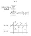
- FIG. 1 illustrates an apparatus for outputting an audio signal according to an exemplary embodiment
- FIGS. 2A and 2B illustrate a method of generating one modulation signal according to an exemplary embodiment
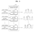
- FIG. 3 illustrates a method of generating a plurality of modulation signals according to an exemplary embodiment
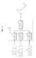
- FIG. 4 illustrates the configuration of the output unit according to an exemplary embodiment
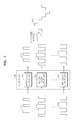
- FIG. 5 illustrates the configuration of an output unit according to another exemplary embodiment
- FIG. 6 is a flowchart illustrating a method of outputting an audio signal according to an exemplary embodiment.
- FIG. 1 illustrates an apparatus for outputting an audio signal according to an exemplary embodiment.
- the apparatus for outputting an audio signal includes a receiving unit 110, a carrier wave generation unit 120, a modulation signal generation unit 130, an amplification unit 140, and an output unit 150.
- the receiving unit 110 receives an audio signal.
- the carrier wave generation unit 120 generates a plurality of carrier waves having different phases using the audio signal received through the receiving unit 110.
- the carrier wave generation unit 120 may generate an initial carrier wave, and then generate phase-shifted carrier waves the respective phases of which are shifted from a phase of the initial carrier wave by predetermined phases, respectively.
- the carrier wave generation unit 120 generates carrier waves such that the initial carrier wave and the phase-shifted carrier waves all have different phases from one another.
- the carrier wave generation unit 120 generates an initial carrier wave, and may then generate a first phase-shifted carrier wave a phase of which is shifted from the phase of the initial carrier wave by 90 degrees, and a second phase-shifted carrier wave a phase of which is shifted from the phase of the initial carrier wave by 180 degrees.
- the carrier wave generation unit 120 may determine a number of carrier waves based on a voltage magnitude of the received audio signal, and generate carrier waves according to the determined number. For example, if the voltage level of the audio signal that is currently inputted through the receiving unit 110 corresponds to volume level 3 of volume levels 1 to 10, the carrier wave generation unit 120 may generate three carrier waves based on the volume level 3. Here, phases of the three carrier waves differ from one another.
- the method of determining the number of the carrier waves is not limited to the example above.
- the carrier wave generation unit 120 may generate the carrier waves the number of which equals the number of output units (not shown) included in the output unit 150.
- the range of volume levels is not limited to one of 1 to 10 as described above, and may be subdivided in increments greater or less than the numerical values of 1 to 10 in another exemplary embodiment.
- the modulation signal generation unit 130 receives the audio signal, and compares the respective carrier waves generated from the carrier wave generation unit 120 with the received audio signal to thereby generate a plurality of modulation signals.
- modulation signal generation unit 130 Detailed operation of the modulation signal generation unit 130 will be described later with reference to FIGS. 2A, 2B and 3 .
- FIGS. 2A and 2B illustrate a method of generating one modulation signal according to an exemplary embodiment.
- FIG. 2A illustrates a carrier wave 210 and an audio signal 220 which are inputted to the modulation signal generation unit 130
- FIG. 2B illustrates a modulation signal 230 that the modulation signal generation unit 130 generates by comparing the carrier wave 210 with the audio signal 220.
- the audio signal 220 is a sinusoidal wave.
- the modulation signal 230 has a high level when a voltage magnitude of the carrier wave 210 is equal to or smaller than that of the audio signal 220, and has a low level when the carrier wave 210 is greater in voltage magnitude than the audio signal 220.
- the modulation signal 230 having a low level means that the voltage magnitude of the modulation signal is smaller than a predetermined threshold value
- the modulation signal 230 having a high level means that the voltage magnitude of the modulation signal is equal to or greater than the predetermined threshold value.
- the modulation signal 230 is not limited to the exemplary embodiment of FIGS. 2A and 2B . Therefore, a modulation signal according to another embodiment may have a low level when the carrier wave 210 is smaller in voltage magnitude than the audio signal 220, and may have a high level when the carrier wave 210 is greater in magnitude than the audio signal 220.
- the modulation signal 230 illustrated in FIG. 2B is a pulse width modulation (PWM) signal.
- the modulation signal generation unit 130 of an exemplary embodiment may generate a PWM signal as illustrated in FIG. 2B , or may generate a modulation signal having different waveforms.
- FIGS. 2A and 2B the method of generating one modulation signal has been described.
- description will be given of a method of generating a plurality of modulation signals with reference to FIG. 3 .
- FIG. 3 illustrates a method of generating a plurality of modulation signals according to an exemplary embodiment.
- the modulation signal generation unit 130 includes N number of modulation units 132, 134, ... , and 136.
- the first modulation unit 132 receives an audio signal and a first carrier wave to generate a first modulation signal 310.
- the second modulation unit 134 receives the audio signal and a second carrier wave to generate a second modulation signal 320.
- the Nth modulation unit 136 receives the audio signal and an Nth carrier wave to generate an Nth modulation signal 330.
- the first to Nth carrier waves 310 to 330 differ in phase from one another.
- high-level periods of some of the first to Nth carrier waves 310 to 330 partly overlap each other.
- the modulation signal generation unit 130 generates modulation signals such that high-level periods of the respective modulation signals partly overlap each other in a time domain.
- the amplification unit 140 amplifies the plurality of modulation signals.
- the amplification unit 140 amplifies amplitudes of voltages or currents of the plurality of modulation signals.
- the modulation signals do not have amplitudes of voltages or currents large enough to drive the output unit 150. For this reason, the amplification unit 140 amplifies voltages or currents of the modulation signals to drive the output unit 150.
- the amplified modulation signals may have voltages or currents having the same magnitude.
- the output unit 150 outputs the amplified modulation signal.
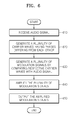
- FIG. 4 illustrates the configuration of the output unit according to an exemplary embodiment.
- the output unit 150 includes N number of voice coils 152a, 152b, ... , and 152c, and an audio output unit 154. That is, the output unit 150 according to an exemplary embodiment may be a speaker including the N number of voice coils 152a, 152b, ... , and 152c, and the audio output unit 154.
- the first voice coil 152a receives a first amplified modulation signal 412 a voltage of which is amplified by the amplification unit 140, and outputs the first amplified modulation signal to the audio output unit 154.
- the second voice coil 152b receives a second amplified modulation signal 414 a voltage of which is amplified by the amplification unit 140, and outputs the second amplified modulation signal to the audio output unit 154.
- the Nth voice coil 152c receives an Nth amplified modulation signal 416 a voltage of which is amplified by the amplification unit 140, and outputs the Nth amplified modulation signal to the audio output unit 154.
- the audio output unit 154 synthesizes the N number of amplified modulation signals 412, 414, ..., and 416 inputted through the N number of voice coils 152a, 152b, ..., and 152c, and outputs a final output signal 420.
- the final output signal 420 illustrated in FIG. 4 is an output signal obtained when the audio signal received by the receiving unit 110 is a sinusoidal wave
- the final output signal 420 also has a waveform similar to the sinusoidal waveform of the received audio signal. Therefore, when the audio signal received by the receiving unit 110 has an arbitrary waveform instead of a sinusoidal waveform, the final output signal 420 also has the arbitrary waveform instead of the sinusoidal waveform.
- the N number of voice coils 152a, 152b, ..., and 152c respectively output the N number of amplified modulation signals 412, 414, ..., and 416 to the audio output unit 154 when the N number of amplified modulation signals 412, 414, ..., and 416 are at logic high.
- the N number of amplified modulation signals 412, 414, ..., and 416 are at logic low, each of the N number of voice coils 152a, 152b, ..., and 152c does not operate, and the N number of amplified modulation signals 412, 414, ..., and 416 have high or low levels at random intervals.
- the conventional method and apparatus must use a complex algorithm such as dynamic element matching (DEM) algorithm in order to overcome the performance difference, which causes computation amount to be increased due to the application of the complex algorithm.
- a complex algorithm such as dynamic element matching (DEM) algorithm
- EDM dynamic element matching
- the performance difference between the voice coils 152a, 152b, ..., and 152c can be prevented without the complex computation that has been necessitated in the conventional method and apparatus.
- FIG. 5 illustrates the configuration of an output unit according to another exemplary embodiment.
- the output unit 150 includes N number of audio output units 151, 153, ..., and 155. That is, the output unit 150 according to an exemplary embodiment may be a speaker including the N number of audio output units 151, 153, ..., and 155.
- the first audio output unit 151 receives a first amplified modulation signal 512 a voltage of which is amplified by the amplification unit 140, and outputs the first amplified modulation signal.
- the second audio output unit 153 receives a second amplified modulation signal 514 a voltage of which is amplified by the amplification unit 140, and outputs the second amplified modulation signal.
- the Nth audio output unit 155 receives an Nth amplified modulation signal 516 a voltage of which is amplified by the amplification unit 140, and outputs the Nth amplified modulation signal.
- N number of audio output units 151, 153, ..., and 155 output N number of amplified modulation signals 512, 514, ..., and 516 spatially
- the outputted N number of amplified modulation signals 512, 514, ..., and 516 are synthesized in space. Therefore, a user located in that space recognizes that the final output signal 520, which is generated by synthesizing the N number of amplified modulation signals 512, 514, ..., and 516 through the output unit 150, is outputted.
- the N number of audio output units 151, 153, ..., and 155 respectively output the N number of amplified modulation signals 512, 514, ..., and 516 spatially when the N number of amplified modulation signals 512, 514, ..., and 516 are at logic high.
- the N number of amplified modulation signals 512, 514, ..., and 516 are at logic low, each of the N number of audio output units 151, 153, ..., and 155 does not operate and the N number of amplified modulation signals 412, 414, ..., and 416 have high or low levels at random intervals.
- the conventional method and apparatus must use a complex algorithm such as dynamic element matching (DEM) algorithm in order to overcome the performance difference, which causes computation amount to be increased due to the application of the complex algorithm.
- a complex algorithm such as dynamic element matching (DEM) algorithm
- EDM dynamic element matching
- the performance difference between the audio output units 151, 153, ..., and 155 can be prevented without the complex computation that has been necessitated in the conventional method and apparatus.
- the output unit 150 illustrated in FIGS. 4 and 5 is a speaker employing a half-bridge architecture. However, in the case where the output unit 150 in FIGS. 4 and 5 is a speaker employing a full-bridge architecture, the number of voice coils 152a, 152b, ..., and 152c included in the output unit 150 of FIG. 4 , or the number of audio output units 151, 153, ..., and 155 included in the output unit 150 of FIG. 5 , is reduced.
- the voice coils 152a, 152b, ..., and 152c, or the audio output units 151, 153, ..., and 155 may have a positive input unit and a negative input unit, wherein an amplified modulation signal inputted to the positive input unit may differ in phase by 180 degrees from an amplified modulation signal inputted to the negative input unit.
- a speaker having the half-bridge architecture necessitates four voice coils for outputting four amplified modulation signals
- the speaker having the full-bridge architecture necessitates only two voice coils for outputting four amplified modulation signals.
- the carrier wave generation unit 120 may generate a pair of carrier waves having a phase difference of 180 degrees therebetween.
- FIG. 6 is a flowchart illustrating a method of outputting an audio signal according to an exemplary embodiment.
- an audio signal is received.
- the number of the generated carrier waves may be determined based on a voltage magnitude of the received audio signal.
- a plurality of modulation signals are generated by comparing the respective carrier waves with the audio signal.
- the modulation signals are generated such that high-level periods of the respective modulation signals partly overlap each other in a time domain.
- the plurality of modulation signals are amplified.
- the amplified modulation signals are outputted.
- exemplary embodiments may be written as a program to be performed by a computer.
- exemplary embodiments may be realized at a general-purpose computer which operates the program.
- the computer-readable recording medium includes, but is not limited to, a magnetic storage medium (e.g., ROM, floppy disk, hard disk and the like) and an optical reading medium (e.g., CD-ROM, DVD and the like).
- a magnetic storage medium e.g., ROM, floppy disk, hard disk and the like
- an optical reading medium e.g., CD-ROM, DVD and the like
Landscapes
- Engineering & Computer Science (AREA)
- Power Engineering (AREA)
- Signal Processing (AREA)
- Amplifiers (AREA)
Applications Claiming Priority (1)
| Application Number | Priority Date | Filing Date | Title |
|---|---|---|---|
| KR1020100001898A KR101664431B1 (ko) | 2010-01-08 | 2010-01-08 | 오디오 신호 출력 방법 및 그 장치 |
Publications (2)
| Publication Number | Publication Date |
|---|---|
| EP2355352A1 true EP2355352A1 (fr) | 2011-08-10 |
| EP2355352B1 EP2355352B1 (fr) | 2013-03-20 |
Family
ID=43901274
Family Applications (1)
| Application Number | Title | Priority Date | Filing Date |
|---|---|---|---|
| EP10189946A Not-in-force EP2355352B1 (fr) | 2010-01-08 | 2010-11-04 | Procédé et appareil pour la sortie d'un signal audio |
Country Status (3)
| Country | Link |
|---|---|
| US (1) | US8625821B2 (fr) |
| EP (1) | EP2355352B1 (fr) |
| KR (1) | KR101664431B1 (fr) |
Families Citing this family (1)
| Publication number | Priority date | Publication date | Assignee | Title |
|---|---|---|---|---|
| KR101683174B1 (ko) * | 2010-01-08 | 2016-12-06 | 삼성전자주식회사 | 오디오 신호 증폭 방법 및 그 장치 |
Citations (3)
| Publication number | Priority date | Publication date | Assignee | Title |
|---|---|---|---|---|
| US4164714A (en) * | 1977-09-26 | 1979-08-14 | Harris Corporation | Polyphase PDM amplifier |
| US5216376A (en) * | 1992-06-10 | 1993-06-01 | Harris Corporation | Pulse duration amplifier system having distortion reduction |
| JP2001127562A (ja) * | 1999-10-25 | 2001-05-11 | Susumu Kimura | Pwm電力増幅器 |
Family Cites Families (3)
| Publication number | Priority date | Publication date | Assignee | Title |
|---|---|---|---|---|
| US4580111A (en) * | 1981-12-24 | 1986-04-01 | Harris Corporation | Amplitude modulation using digitally selected carrier amplifiers |
| TWI340286B (en) * | 2006-10-12 | 2011-04-11 | Chunghwa Picture Tubes Ltd | Pixel structure |
| KR101683174B1 (ko) * | 2010-01-08 | 2016-12-06 | 삼성전자주식회사 | 오디오 신호 증폭 방법 및 그 장치 |
-
2010
- 2010-01-08 KR KR1020100001898A patent/KR101664431B1/ko not_active Expired - Fee Related
- 2010-07-13 US US12/835,176 patent/US8625821B2/en active Active
- 2010-11-04 EP EP10189946A patent/EP2355352B1/fr not_active Not-in-force
Patent Citations (4)
| Publication number | Priority date | Publication date | Assignee | Title |
|---|---|---|---|---|
| US4164714A (en) * | 1977-09-26 | 1979-08-14 | Harris Corporation | Polyphase PDM amplifier |
| US4164714B1 (fr) * | 1977-09-26 | 1984-12-25 | ||
| US5216376A (en) * | 1992-06-10 | 1993-06-01 | Harris Corporation | Pulse duration amplifier system having distortion reduction |
| JP2001127562A (ja) * | 1999-10-25 | 2001-05-11 | Susumu Kimura | Pwm電力増幅器 |
Also Published As
| Publication number | Publication date |
|---|---|
| US20110170719A1 (en) | 2011-07-14 |
| KR20110081641A (ko) | 2011-07-14 |
| US8625821B2 (en) | 2014-01-07 |
| KR101664431B1 (ko) | 2016-10-10 |
| EP2355352B1 (fr) | 2013-03-20 |
Similar Documents
| Publication | Publication Date | Title |
|---|---|---|
| US8000824B2 (en) | Audio reproducing apparatus | |
| US8204239B2 (en) | Audio processing method and audio processing apparatus | |
| US8866544B2 (en) | Class D pulse width modulator with dual feedback | |
| JP2010206348A (ja) | デューティ比補正回路及びデューティ比補正方法 | |
| US11342892B2 (en) | Amplifier and signal processing circuit | |
| US8378198B2 (en) | Method and apparatus for detecting pitch period of input signal | |
| CN100553122C (zh) | 多通道数字放大器、其信号处理方法及其音频再现系统 | |
| EP2355352A1 (fr) | Procédé et appareil pour la sortie d'un signal audio | |
| JP4201752B2 (ja) | オーディオパワーアンプic | |
| JP4882353B2 (ja) | パルス幅変調増幅器 | |
| EP1781069A2 (fr) | Procédé de mesure d'une caractéristique de fréquence et du flanc montant de la réponse impulsionnelle ainsi que dispositif pour la correction d'un champ acoustique | |
| JP6301592B2 (ja) | 故障検出装置 | |
| JP7332945B2 (ja) | 音場生成装置、音場生成方法、及び音場生成プログラム | |
| US9130513B2 (en) | Method and apparatus for amplifying audio signal | |
| JP6304942B2 (ja) | 電力変換装置、電力変換装置の制御方法及び制御プログラム | |
| US20220223138A1 (en) | Combined wave data generation method, combined wave data generation program, storage medium, combined wave data generation device, and waveform data generation method | |
| Casazza et al. | Infinite dimensional restricted invertibility | |
| JP2014057208A (ja) | スウィープ信号生成装置、スウィープ信号生成方法、及びプログラム | |
| WO2019111703A1 (fr) | Dispositif de traitement de signal, procédé de traitement de signal et programme | |
| JP6565488B2 (ja) | 差動信号をシングルエンド信号に変換する回路及び方法 | |
| JP4222492B2 (ja) | オーディオパワーアンプic及びそれを備えたオーディオシステム | |
| JP5310498B2 (ja) | 音響信号に対する情報の埋め込み装置 | |
| US20150380633A1 (en) | Apparatus for driving piezoelectric element and method for driving piezoelectric element | |
| JP2011180234A (ja) | 音響信号に対する情報の埋め込み装置 | |
| JP4985380B2 (ja) | 信号生成装置およびd級増幅装置 |
Legal Events
| Date | Code | Title | Description |
|---|---|---|---|
| PUAI | Public reference made under article 153(3) epc to a published international application that has entered the european phase |
Free format text: ORIGINAL CODE: 0009012 |
|
| AK | Designated contracting states |
Kind code of ref document: A1 Designated state(s): AL AT BE BG CH CY CZ DE DK EE ES FI FR GB GR HR HU IE IS IT LI LT LU LV MC MK MT NL NO PL PT RO RS SE SI SK SM TR |
|
| AX | Request for extension of the european patent |
Extension state: BA ME |
|
| 17P | Request for examination filed |
Effective date: 20120209 |
|
| 17Q | First examination report despatched |
Effective date: 20120316 |
|
| RAP1 | Party data changed (applicant data changed or rights of an application transferred) |
Owner name: SAMSUNG ELECTRONICS CO., LTD. |
|
| GRAP | Despatch of communication of intention to grant a patent |
Free format text: ORIGINAL CODE: EPIDOSNIGR1 |
|
| GRAS | Grant fee paid |
Free format text: ORIGINAL CODE: EPIDOSNIGR3 |
|
| GRAA | (expected) grant |
Free format text: ORIGINAL CODE: 0009210 |
|
| AK | Designated contracting states |
Kind code of ref document: B1 Designated state(s): AL AT BE BG CH CY CZ DE DK EE ES FI FR GB GR HR HU IE IS IT LI LT LU LV MC MK MT NL NO PL PT RO RS SE SI SK SM TR |
|
| REG | Reference to a national code |
Ref country code: GB Ref legal event code: FG4D |
|
| REG | Reference to a national code |
Ref country code: CH Ref legal event code: EP |
|
| REG | Reference to a national code |
Ref country code: IE Ref legal event code: FG4D |
|
| REG | Reference to a national code |
Ref country code: AT Ref legal event code: REF Ref document number: 602599 Country of ref document: AT Kind code of ref document: T Effective date: 20130415 |
|
| REG | Reference to a national code |
Ref country code: DE Ref legal event code: R096 Ref document number: 602010005566 Country of ref document: DE Effective date: 20130516 |
|
| PG25 | Lapsed in a contracting state [announced via postgrant information from national office to epo] |
Ref country code: BG Free format text: LAPSE BECAUSE OF FAILURE TO SUBMIT A TRANSLATION OF THE DESCRIPTION OR TO PAY THE FEE WITHIN THE PRESCRIBED TIME-LIMIT Effective date: 20130620 Ref country code: ES Free format text: LAPSE BECAUSE OF FAILURE TO SUBMIT A TRANSLATION OF THE DESCRIPTION OR TO PAY THE FEE WITHIN THE PRESCRIBED TIME-LIMIT Effective date: 20130701 Ref country code: NO Free format text: LAPSE BECAUSE OF FAILURE TO SUBMIT A TRANSLATION OF THE DESCRIPTION OR TO PAY THE FEE WITHIN THE PRESCRIBED TIME-LIMIT Effective date: 20130620 Ref country code: LT Free format text: LAPSE BECAUSE OF FAILURE TO SUBMIT A TRANSLATION OF THE DESCRIPTION OR TO PAY THE FEE WITHIN THE PRESCRIBED TIME-LIMIT Effective date: 20130320 Ref country code: SE Free format text: LAPSE BECAUSE OF FAILURE TO SUBMIT A TRANSLATION OF THE DESCRIPTION OR TO PAY THE FEE WITHIN THE PRESCRIBED TIME-LIMIT Effective date: 20130320 |
|
| REG | Reference to a national code |
Ref country code: AT Ref legal event code: MK05 Ref document number: 602599 Country of ref document: AT Kind code of ref document: T Effective date: 20130320 |
|
| REG | Reference to a national code |
Ref country code: LT Ref legal event code: MG4D |
|
| PG25 | Lapsed in a contracting state [announced via postgrant information from national office to epo] |
Ref country code: GR Free format text: LAPSE BECAUSE OF FAILURE TO SUBMIT A TRANSLATION OF THE DESCRIPTION OR TO PAY THE FEE WITHIN THE PRESCRIBED TIME-LIMIT Effective date: 20130621 Ref country code: FI Free format text: LAPSE BECAUSE OF FAILURE TO SUBMIT A TRANSLATION OF THE DESCRIPTION OR TO PAY THE FEE WITHIN THE PRESCRIBED TIME-LIMIT Effective date: 20130320 Ref country code: LV Free format text: LAPSE BECAUSE OF FAILURE TO SUBMIT A TRANSLATION OF THE DESCRIPTION OR TO PAY THE FEE WITHIN THE PRESCRIBED TIME-LIMIT Effective date: 20130320 Ref country code: SI Free format text: LAPSE BECAUSE OF FAILURE TO SUBMIT A TRANSLATION OF THE DESCRIPTION OR TO PAY THE FEE WITHIN THE PRESCRIBED TIME-LIMIT Effective date: 20130320 |
|
| REG | Reference to a national code |
Ref country code: NL Ref legal event code: VDEP Effective date: 20130320 |
|
| PG25 | Lapsed in a contracting state [announced via postgrant information from national office to epo] |
Ref country code: RS Free format text: LAPSE BECAUSE OF FAILURE TO SUBMIT A TRANSLATION OF THE DESCRIPTION OR TO PAY THE FEE WITHIN THE PRESCRIBED TIME-LIMIT Effective date: 20130320 Ref country code: BE Free format text: LAPSE BECAUSE OF FAILURE TO SUBMIT A TRANSLATION OF THE DESCRIPTION OR TO PAY THE FEE WITHIN THE PRESCRIBED TIME-LIMIT Effective date: 20130320 Ref country code: HR Free format text: LAPSE BECAUSE OF FAILURE TO SUBMIT A TRANSLATION OF THE DESCRIPTION OR TO PAY THE FEE WITHIN THE PRESCRIBED TIME-LIMIT Effective date: 20130320 |
|
| PG25 | Lapsed in a contracting state [announced via postgrant information from national office to epo] |
Ref country code: IS Free format text: LAPSE BECAUSE OF FAILURE TO SUBMIT A TRANSLATION OF THE DESCRIPTION OR TO PAY THE FEE WITHIN THE PRESCRIBED TIME-LIMIT Effective date: 20130720 Ref country code: CZ Free format text: LAPSE BECAUSE OF FAILURE TO SUBMIT A TRANSLATION OF THE DESCRIPTION OR TO PAY THE FEE WITHIN THE PRESCRIBED TIME-LIMIT Effective date: 20130320 Ref country code: NL Free format text: LAPSE BECAUSE OF FAILURE TO SUBMIT A TRANSLATION OF THE DESCRIPTION OR TO PAY THE FEE WITHIN THE PRESCRIBED TIME-LIMIT Effective date: 20130320 Ref country code: SK Free format text: LAPSE BECAUSE OF FAILURE TO SUBMIT A TRANSLATION OF THE DESCRIPTION OR TO PAY THE FEE WITHIN THE PRESCRIBED TIME-LIMIT Effective date: 20130320 Ref country code: RO Free format text: LAPSE BECAUSE OF FAILURE TO SUBMIT A TRANSLATION OF THE DESCRIPTION OR TO PAY THE FEE WITHIN THE PRESCRIBED TIME-LIMIT Effective date: 20130320 Ref country code: PT Free format text: LAPSE BECAUSE OF FAILURE TO SUBMIT A TRANSLATION OF THE DESCRIPTION OR TO PAY THE FEE WITHIN THE PRESCRIBED TIME-LIMIT Effective date: 20130722 Ref country code: EE Free format text: LAPSE BECAUSE OF FAILURE TO SUBMIT A TRANSLATION OF THE DESCRIPTION OR TO PAY THE FEE WITHIN THE PRESCRIBED TIME-LIMIT Effective date: 20130320 Ref country code: AT Free format text: LAPSE BECAUSE OF FAILURE TO SUBMIT A TRANSLATION OF THE DESCRIPTION OR TO PAY THE FEE WITHIN THE PRESCRIBED TIME-LIMIT Effective date: 20130320 |
|
| PG25 | Lapsed in a contracting state [announced via postgrant information from national office to epo] |
Ref country code: PL Free format text: LAPSE BECAUSE OF FAILURE TO SUBMIT A TRANSLATION OF THE DESCRIPTION OR TO PAY THE FEE WITHIN THE PRESCRIBED TIME-LIMIT Effective date: 20130320 Ref country code: CY Free format text: LAPSE BECAUSE OF FAILURE TO SUBMIT A TRANSLATION OF THE DESCRIPTION OR TO PAY THE FEE WITHIN THE PRESCRIBED TIME-LIMIT Effective date: 20130320 |
|
| PLBE | No opposition filed within time limit |
Free format text: ORIGINAL CODE: 0009261 |
|
| STAA | Information on the status of an ep patent application or granted ep patent |
Free format text: STATUS: NO OPPOSITION FILED WITHIN TIME LIMIT |
|
| PG25 | Lapsed in a contracting state [announced via postgrant information from national office to epo] |
Ref country code: DK Free format text: LAPSE BECAUSE OF FAILURE TO SUBMIT A TRANSLATION OF THE DESCRIPTION OR TO PAY THE FEE WITHIN THE PRESCRIBED TIME-LIMIT Effective date: 20130320 |
|
| 26N | No opposition filed |
Effective date: 20140102 |
|
| PG25 | Lapsed in a contracting state [announced via postgrant information from national office to epo] |
Ref country code: IT Free format text: LAPSE BECAUSE OF FAILURE TO SUBMIT A TRANSLATION OF THE DESCRIPTION OR TO PAY THE FEE WITHIN THE PRESCRIBED TIME-LIMIT Effective date: 20130320 |
|
| REG | Reference to a national code |
Ref country code: DE Ref legal event code: R097 Ref document number: 602010005566 Country of ref document: DE Effective date: 20140102 |
|
| PG25 | Lapsed in a contracting state [announced via postgrant information from national office to epo] |
Ref country code: MC Free format text: LAPSE BECAUSE OF FAILURE TO SUBMIT A TRANSLATION OF THE DESCRIPTION OR TO PAY THE FEE WITHIN THE PRESCRIBED TIME-LIMIT Effective date: 20130320 |
|
| REG | Reference to a national code |
Ref country code: FR Ref legal event code: ST Effective date: 20140731 |
|
| REG | Reference to a national code |
Ref country code: IE Ref legal event code: MM4A |
|
| PG25 | Lapsed in a contracting state [announced via postgrant information from national office to epo] |
Ref country code: IE Free format text: LAPSE BECAUSE OF NON-PAYMENT OF DUE FEES Effective date: 20131104 |
|
| PG25 | Lapsed in a contracting state [announced via postgrant information from national office to epo] |
Ref country code: FR Free format text: LAPSE BECAUSE OF NON-PAYMENT OF DUE FEES Effective date: 20131202 |
|
| PG25 | Lapsed in a contracting state [announced via postgrant information from national office to epo] |
Ref country code: SM Free format text: LAPSE BECAUSE OF FAILURE TO SUBMIT A TRANSLATION OF THE DESCRIPTION OR TO PAY THE FEE WITHIN THE PRESCRIBED TIME-LIMIT Effective date: 20130320 |
|
| PG25 | Lapsed in a contracting state [announced via postgrant information from national office to epo] |
Ref country code: TR Free format text: LAPSE BECAUSE OF FAILURE TO SUBMIT A TRANSLATION OF THE DESCRIPTION OR TO PAY THE FEE WITHIN THE PRESCRIBED TIME-LIMIT Effective date: 20130320 |
|
| REG | Reference to a national code |
Ref country code: CH Ref legal event code: PL |
|
| PG25 | Lapsed in a contracting state [announced via postgrant information from national office to epo] |
Ref country code: CH Free format text: LAPSE BECAUSE OF NON-PAYMENT OF DUE FEES Effective date: 20141130 Ref country code: HU Free format text: LAPSE BECAUSE OF FAILURE TO SUBMIT A TRANSLATION OF THE DESCRIPTION OR TO PAY THE FEE WITHIN THE PRESCRIBED TIME-LIMIT; INVALID AB INITIO Effective date: 20101104 Ref country code: LU Free format text: LAPSE BECAUSE OF NON-PAYMENT OF DUE FEES Effective date: 20131104 Ref country code: LI Free format text: LAPSE BECAUSE OF NON-PAYMENT OF DUE FEES Effective date: 20141130 Ref country code: MK Free format text: LAPSE BECAUSE OF FAILURE TO SUBMIT A TRANSLATION OF THE DESCRIPTION OR TO PAY THE FEE WITHIN THE PRESCRIBED TIME-LIMIT Effective date: 20130320 |
|
| PG25 | Lapsed in a contracting state [announced via postgrant information from national office to epo] |
Ref country code: MT Free format text: LAPSE BECAUSE OF FAILURE TO SUBMIT A TRANSLATION OF THE DESCRIPTION OR TO PAY THE FEE WITHIN THE PRESCRIBED TIME-LIMIT Effective date: 20130320 |
|
| PGFP | Annual fee paid to national office [announced via postgrant information from national office to epo] |
Ref country code: DE Payment date: 20171018 Year of fee payment: 8 |
|
| PGFP | Annual fee paid to national office [announced via postgrant information from national office to epo] |
Ref country code: GB Payment date: 20171019 Year of fee payment: 8 |
|
| PG25 | Lapsed in a contracting state [announced via postgrant information from national office to epo] |
Ref country code: AL Free format text: LAPSE BECAUSE OF FAILURE TO SUBMIT A TRANSLATION OF THE DESCRIPTION OR TO PAY THE FEE WITHIN THE PRESCRIBED TIME-LIMIT Effective date: 20130320 |
|
| REG | Reference to a national code |
Ref country code: DE Ref legal event code: R119 Ref document number: 602010005566 Country of ref document: DE |
|
| GBPC | Gb: european patent ceased through non-payment of renewal fee |
Effective date: 20181104 |
|
| PG25 | Lapsed in a contracting state [announced via postgrant information from national office to epo] |
Ref country code: DE Free format text: LAPSE BECAUSE OF NON-PAYMENT OF DUE FEES Effective date: 20190601 |
|
| PG25 | Lapsed in a contracting state [announced via postgrant information from national office to epo] |
Ref country code: GB Free format text: LAPSE BECAUSE OF NON-PAYMENT OF DUE FEES Effective date: 20181104 |