EP2351237B1 - Verfahren und vorrichtung zur messung der parameter eines systems zur ausbreitung des spektrums eines taktsignals - Google Patents
Verfahren und vorrichtung zur messung der parameter eines systems zur ausbreitung des spektrums eines taktsignals Download PDFInfo
- Publication number
- EP2351237B1 EP2351237B1 EP09820275.7A EP09820275A EP2351237B1 EP 2351237 B1 EP2351237 B1 EP 2351237B1 EP 09820275 A EP09820275 A EP 09820275A EP 2351237 B1 EP2351237 B1 EP 2351237B1
- Authority
- EP
- European Patent Office
- Prior art keywords
- signal
- modulation
- counter
- occurrence
- determining
- Prior art date
- Legal status (The legal status is an assumption and is not a legal conclusion. Google has not performed a legal analysis and makes no representation as to the accuracy of the status listed.)
- Active
Links
Images

Classifications
-
- H—ELECTRICITY
- H03—ELECTRONIC CIRCUITRY
- H03K—PULSE TECHNIQUE
- H03K5/00—Manipulating of pulses not covered by one of the other main groups of this subclass
- H03K5/19—Monitoring patterns of pulse trains
Definitions
- the present disclosure generally relates to electronic circuits and, more specifically, to circuits comprising elements for generating one or several periodic signals implementing a method for spreading the spectrum of the radiation of the periodic signal(s).
- the present disclosure more specifically relates to the estimating of the parameters of a method for spreading the spectrum of periodic signals.
- Synchronous electronic circuits are generally clocked by at least one clock signal.
- such circuits may emit an electromagnetic radiation having a spectrum which comprises a main line at the frequency of the clock signal and secondary lines at the harmonics.
- the spectral line at the frequency of the clock signal concentrates most of the radiated power. This may result in electromagnetic interferences with adjacent electronic circuits. Such is the case, for example, for electronic circuits comprising high-speed series connections which may emit a radiation disturbing adjacent circuits.
- SSC method Spread Spectrum Clocking
- An SSC method generally comprises carrying out a modulation of the frequency of the clock signal or SSC modulation.
- the clock frequency is modulated by a periodic triangular signal defined by two parameters: modulation period T mod and modulation ratio R mod .
- Ratio R mod is generally defined as being the ratio of half the difference between the maximum clock frequency and the minimum clock frequency to a reference frequency, for example, the average frequency of the clock signal.
- a difficulty is to estimate the parameters of an SSC method implemented by an electronic circuit. Indeed, while it is relatively easy to acknowledge the absence of implementation of an SSC by spectral analysis of the radiation emitted by an electronic circuit, it is more difficult to determine the parameters of the SSC method based on the analysis of the clock signal of the circuit to determine whether the SSC method actually implemented corresponds to the expected SSC method. This can generally only be performed by means of relatively complex dedicated tools, the use of which, in terms of cost and duration, cannot be envisaged to test electronic circuits manufactured at an industrial scale.
- Publication US 2005/0071132 discloses a method of measuring the FM profiles of a work signal.
- Publication EP 1 841 066 discloses a method of measuring the jitter of a first periodic signal with respect to a second periodic signal.
- the present disclosure aims at a method for estimating the parameters of an SSC modulation used by an electronic circuit, of simple, fast, and cost-effective implementation.
- the present disclosure also aims at a device for estimating the parameters of an SSC modulation implemented by an electronic circuit which causes only few modifications of the electronic circuit.
- an embodiment provides a method for estimating parameters of a system for spreading the spectrum of a first periodic signal according to a modulation period.
- the method comprises the steps of sampling the first signal by means of a second periodic signal, of determining based on the sampling result each occurrence where the first and second signals are synchronous, of incrementing a first counter at each sampling, the first counter being reset at each said occurrence, of storing at each said occurrence the last value of the first counter before resetting, of providing a third periodic signal at a first level when said last value is greater than a threshold and at a second level when said last value is smaller than the threshold, and of determining the modulation period based on the period of the third signal.
- the spreading system is further defined by a modulation ratio.
- the method further comprises the steps of incrementing a second counter at each said occurrence, incrementing a third counter at each said occurrence according to the comparison of said last value and of the threshold, and determining the modulation ratio based on the ratio of the third and second counters.
- the method further comprises the steps of determining a first time period corresponding to a determined number of cycles of the second periodic signal, determining a second time period corresponding to the determined number of cycles of a third periodic signal at the same frequency as the second periodic signal and having no jitter, and correcting the modulation period and the modulation ratio based on the ratio between the second and first time periods.
- the method further comprises the steps of providing the result of the sampling to the input of a shift register triggered by the second signal, determining a first quantity corresponding to the number of bits of a current word formed from parallel outputs of the shift register in a first state and a second quantity corresponding to the number of bits of the current word in a second state, and counting the number of occurrences of an equality of the first and second quantities.
- the method further comprises the steps of providing the result of the sampling to the input of a shift register triggered by the second signal, comparing at least first states and last states of a current word formed from parallel outputs of the shift register with at least one reference word, and counting the number of occurrences of the reference word.
- the first and last bits of the reference word are in inverse states.
- the reference word comprises first and second bits halves, each comprising a same number of bits in a first state and a same number of bits in a second state.
- the number of bits of the reference word ranges between four and twelve.
- An embodiment also provides a device for estimating parameters of a system for spreading the spectrum of a first periodic signal according to a modulation period.
- the device comprises a shift register having an input receiving the first periodic signal, sampled by a second periodic signal, a unit for determining, based on the sampling result, each occurrence where the first and second signals are synchronous, a first counter of each sampling reset at each said occurrence, a memory containing the last value of the first counter before resetting at each said occurrence, a unit for determining a third binary signal at a first level when said last value is greater than a threshold and at a second level when said last value is smaller than the threshold and a unit for determining the modulation period based on the period of the third signal.
- the spreading system is further defined by a modulation ratio.
- the device further comprises a second counter of each said occurrence, a third counter of each said occurrence when said last value is greater or smaller than the threshold, and a unit for determining the modulation ratio based on the ratio of the third and second counters.
- a system comprises: means for generating a spread spectrum clock signal; and means for estimating a modulation period of the spread spectrum clock signal, the means for estimating having: means for sampling the spread spectrum clock signal using a sampling clock signal; means for tracking occurrences of synchronization between the spread spectrum clock signal and the sampling clock signal; and means for generating a binary signal based on the tracking of occurrences of synchronization.
- the means for sampling comprises a shift register.
- the means for tracking comprises a pattern detector.
- the means for tracking comprises a counter.
- the means for generating a binary signal comprises a comparator.
- the system further comprises means for estimating a modulation ratio of the spread spectrum clock signal.
- a system comprises: a spread spectrum clock generator configured to generate a spread spectrum clock signal; and a modulation period estimator having: a sampler configured to sample the spread spectrum clock signal using a sampling signal; a synchronization detector configured to detect occurrences of synchronization between the spread spectrum clock signal and the sampling signal; and a modulation period detector configured to estimate a modulation period of the spread spectrum clock signal based on the detected occurrences.
- the sampler comprises a plurality of flip-flops.
- the synchronization detector comprises a shift register and a pattern detector.
- the modulation period detector comprises: a sampling counter configured to count cycles of the sampling clock; a memory configured to store an output of the sampling counter; and a comparator configured to compare the stored output of the sampling counter to a threshold and generate a signal indicative of the modulation period based on the comparison.
- the modulation period detector further comprises a counter configured to count transitions of the signal indicative of the modulation period from a low state to a high state.
- the system further comprises: a modulation ratio estimator configured to estimate a modulation ratio of the spread spectrum clock signal.
- the modulation ratio estimator comprises: a synchronization occurrence counter configured to count detected occurrences of synchronization; a threshold counter configured to count occurrences of the stored output of the sampling counter being less than the threshold; and a divider coupled to the synchronization occurrence counter and to the threshold counter.
- the modulation period estimator is configured to compensate for jitter in the sampling signal.
- a method of estimating a modulation period of a spread spectrum clock in an electronic device comprises: sampling the spread spectrum clock signal with a sampling clock signal; tracking occurrences of synchronization between the spread spectrum clock signal and the sampling clock signal; generating a periodic signal based on the tracking of occurrences of synchronization; and estimating the modulation period based on a period of the generated period signal.
- the method further comprises: counting occurrences of synchronization; and estimating a modulation ratio of the spread spectrum signal based on the counting of occurrences of synchronization.
- FIG. 1 shows an embodiment of a circuit 10 for providing a clock signal CK out implementing an SSC modulation.
- Circuit 10 corresponds to a phase-locked loop (PLL) receiving a clock signal CK in and delivering clock signal CK out at a frequency F out .
- Clock signal CK in is, for example, a signal provided by a piezoelectric oscillator.
- Circuit 10 comprises a phase comparator 12 receiving at one input clock signal CK in and a signal S I and delivering a signal S C representative of the phase difference between signals CK in and S I .
- Signal Sc drives a low-pass filter 14 which provides, from a signal S C , a control signal S' C to a voltage-controlled oscillator 16 (VCO).
- Oscillator 16 delivers clock signal CK out at a frequency which depends on signal S' C .
- a divider 18 receives signal CK out and delivers signal S I , having a frequency equal to the frequency of signal CK out divided by a division
- circuit 10 comprises a spread spectrum clocking circuit 20 (SSC) which provides divider 18 with a control signal COM.
- Spread spectrum clocking circuit 20 can receive signal S I .
- Divider 18 is capable of modifying factor M according to signal COM. The variation of factor M translates as a modulation of frequency F osc of signal CK out around a central frequency F 0 .
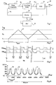
- Figure 2 illustrates an example of a curve 22 of the variation of oscillation frequency F osc of signal CK out for an example of an SSC modulation.
- Frequency F osc varies between a minimum frequency F 1 and a maximum frequency F 2 around central frequency F 0 according to a periodic triangular modulation of period T mod (corresponding to a frequency F mod ).
- Call modulation ratio R mod the ratio of half the difference between frequencies F 2 and F 1 to central frequency F 0 .
- modulation ratio R mod may correspond to the ratio of the difference between frequencies F 2 and F 1 to frequency F 2 or F 1 .
- the modulation may be sinusoidal. It is then also defined by modulation period T mod and modulation ratio R mod .
- An estimation method comprises determining, based on an analysis of the clock signal to which an SSC modulation is applied, parameters T mod and R mod of the SSC modulation implemented by spread spectrum clocking circuit 20. For this purpose, the observed signal to which the SSC modulation is applied is compared with a periodic reference signal CK ref .
- Periodic reference signal CK ref may be a signal provided by a circuit for generating a periodic signal. It is for example a clock signal directly provided by a piezoelectric oscillator, a clock signal provided by a phase-locked loop, etc.
- Figure 3 shows timing diagrams of an example of an observed periodic signal CK obs to which an SSC modulation is applied, for example, the SSC modulation of Figure 2 , and of a periodic reference signal CK ref of frequency F ref and of period T ref .
- signals CK obs and CK ref are binary signals varying between two states, a high state (state "1") and a low state (state "0").
- the signal edges are assumed to be instantaneous. In practice, they follow a slope between the two high and low states and conversely. This however does not change the principles.
- An estimation method uses a BCC counter which is incremented on each rising (or falling) edge of reference clock signal CK ref and which is reset each time signals CK obs and CK ref are synchronous.
- the value of the BCC counter before resetting, called BCCm corresponds to the number of rising (or falling) edges of reference clock signal CK ref in time TB.
- Figure 4 shows an example of a curve 30 of the variation of value BCCm according to the rising edges of reference signal CK ref when the SSC modulation is of the type shown in Figure 2 .
- frequency F ref of reference signal CK ref is slightly greater than maximum frequency F 2 of observed signal CK obs .
- frequency F ref is of 607.5 MHz
- central frequency F 0 of signal CK obs is 600 MHz
- modulation ratio R mod is of 1%
- modulation frequency F mod is 60 KHz.
- Curve 30 is determined on a operating time window Window and runs through points 31, each point 31 having, as an abscissa, a number of cycles of signal CK ref at which signals CK obs and CK ref are synchronous and, as an ordinate, value BCCm before resetting of the BCC counter. Curve 30 varies periodically at a period equal to modulation period T mod .
- the method comprises comparing value BCCm with a threshold Th and providing a binary signal SSC_Detect in a first state, for example, "1", when value BCCm is greater than threshold Th, and in a second state, for example "0", when value BCCm is smaller than threshold Th.
- Curve 32 illustrates the variation of signal SSC_Detect obtained from curve 30 when threshold Th is equal to 100.
- Signal SSC_Detect is a periodic signal having a period corresponding to modulation period T mod .
- Modulation period T mod of the SSC modulation can thus be obtained by dividing time window Window by the number of rising (or falling) edges of signal SSC_Detect which have occurred during time window Window.
- duty cycle CYC of signal SSC_Detect is linked to modulation ratio R mod by a monotonous function. Thereby, the determination of duty cycle CYC enables to obtain modulation ratio R mod .
- the method according to the present embodiment uses two counters BEC and BTC. Counter BEC is incremented each time a new value BCCm is obtained, that is, each time signals CK obs and CK ref are synchronous. The BTC counter is incremented each time the new value BCCm obtained is smaller than threshold Th. The ratio between the BTC and BEC counters corresponds to duty cycle CYC of signal SSC_Detect.
- Figure 5 shows an example of a curve 34 of the variation of ratio CYC according to modulation ratio R mod obtained for curve 30 and threshold Th of Figure 4 .
- modulation ratio R mod can be obtained from ratio CYC.
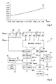
- Figure 6 schematically shows in the form of blocks a testing circuit 35 according to an embodiment.
- Signal CK obs is sampled by at least one first flip-flop 40 and preferably by two flip-flops 40 and 41 in series, data input D of flip-flop 41 being connected to the Q output of flip-flop 40.
- Signal CK ref is applied on the clock inputs of flip-flops 40 and 41.
- a double sampling reduces the uncertainties linked to the set-up and hold times of the flip-flops and to the slopes of the edges of signals CK obs and CK ref .
- a shift register 42 preferentially formed of D flip-flops in series having their respective outputs Q 1 to Q n provided in parallel to a pattern detector 44 (PATTERN DETECT).
- PATTERN DETECT pattern detector 44
- number n of bits of register 42 ranges between four and twelve.
- the function of the detector is to determine from bits Q 1 to Q n when signals CK obs and CK ref are synchronous. This may be obtained by comparing successive bit words Q 1 to Q n with at least one reference pattern, as will be described in further detail hereafter.
- Circuit 44 is connected to a BEC counter 45 and to a BCC counter 46. BCC counter 46 is incremented on each rising edge of reference clock signal CK ref .
- Circuit 35 comprises a memory 48 (Threshold), for example, a register, in which the value of threshold Th is stored.
- Each new value BCCm is compared with threshold Th by a comparator 49.
- Comparator 49 delivers signal SSC_Detect.
- Signal SSC_Detect is, for example, set to the high state when value BCCm is greater than threshold Th and set to the low state when value BCCm is smaller than threshold Th.
- Circuit 35 comprises a unit 50 (T mod Detect) which detects when signal SSC_Detect switches from the low state to the high state (or from the high state to the low state).
- unit 50 comprises a counter which is incremented each time signal SSC_Detect switches from the low state to the high state.
- Circuit 35 comprises BTC counter 51 which is incremented for each determination of a new value BCCm, when this value is smaller than threshold Th.
- the values of the BTC and BEC counters are provided to a divider 52 (DIV) which determines the ratio between the BTC counter and the BEC counter, this ratio being stored in a memory 53 (BTC/BEC).
- Circuit 35 comprises a memory 54 (End) in which is stored the total number TOT of cycles of reference clock signal CK ref during which circuit 35 operates.
- the BEC counter is compared with threshold TOT by a comparator 55 which provides a signal Win_open.
- signal Win_open is set to a first state, for example, "0”, when the BEC counter is smaller than threshold TOT and set to a second state, for example "1", when the BEC counter is greater than or equal to threshold TOT.
- Modulation period T mod is, for example, obtained by dividing the duration of operating time window Window, that is, the duration for which signal Win_open is at "0", by the value of counter 50.
- Modulation ratio R mod is obtained from the value stored in memory 53 at the end of operating time window Window and curve 34 which may be stored in a memory of Look-up Table type, not shown.
- modulation period T mod and of modulation ratio R mod provided by circuit 35 may be compared with reference values. Too large an interval with respect to the reference values means that the SSC modulation applied to observed signal CK obs does not correspond to the expected SSC modulation.
- the detection by circuit 35 of a synchronous edge between signals CK obs and CK ref may be performed by considering that the samples of signal CK obs which come before a synchronous edge and the samples of signal CK obs which follow a synchronous edge have inverse values.
- An embodiment provides comparing the word contained in shift register 42, driven by reference signal CK ref , and having its data input receiving the sampled signal to be measured CK obs , with a reference pattern to estimate the presence of a common rising edge between signals CK ref and CK obs .
- the reference pattern comprises an even number of bits distributed in a first bit half and a second bit half.
- the present embodiment provides detecting the presence of a synchronous edge between signals CK ref and CK obs which substantially occurs at half of the word contained in shift register 42.
- the bits of the first half of the reference pattern are in a same state and the bits of the second half of the reference pattern are in the inverse state.
- Figure 7 schematically shows an example of a detection circuit 44.
- this circuit comprises a comparator 60 (COMP) of word Q 1 to Q n provided by register 42 (possibly transiting through a temporary storage element 62) with respect to a reference word, for example stored in a storage element 63 or cabled in the circuit.
- first bit half B 1 to B n/2 is in a first state, for example "1”
- second bit half B n/2+1 to B n is in the inverse state, for example "0”.
- the pattern is compared with the words successively present on the outputs of shift register 42 and the frequency of its occurrence indicates the number of synchronous edges between signals CK ref and CK obs .
- Figure 8 illustrates examples of reference patterns that may be used by comparator 60 to take into account fluctuations of signal CK obs .
- bit B 1 to B n/2-1 are at “1” and bits Bn /2+2 to B n are at “0”.
- Bit B n/2 is at "0” and bit B n/2+1 is at “1”.
- bits B 1 to B n/2-2 are at “1” and bits B n/2+3 to B n are at "0”.
- Bits B n/2-1 and B n/2+1 are at "0” and bits B n/2 and B n/2+2 are at “1".
- detection circuit 44 counts the number of bits at "0" and the number of bits at "1" of the word contained in shift register 42.
- Signals CK ref and CK obs are considered to be synchronous in the case where the number of bits at "0" is equal to the number of bits at "1".
- reference signal CK ref has been considered to be approximately selected with a frequency on the same order of magnitude as signal CK obs to be observed.
- Figure 9 is a drawing similar to Figure 3 in which a reference signal CK' ref having a frequency F' ref smaller than frequency F ref of signal CK ref by a factor K equal to 2 has further been shown. More generally, factor K may be a real number greater than or equal to 2.
- signal CK' ref is used, the operation of test circuit 35 is identical to what has been previously described. However, as compared with the embodiment previously described in relation with Figure 4 , the obtained values BCCm are divided by factor K, given that signal CK obs to be observed is sampled less often.
- the measurements performed by the previously-described test method may be influenced by the jitter which affects reference clock signal CK ref .
- modulation period T mod and modulation ratio R mod provided by circuit 35 are referenced to signal CK ref .
- the test method according to the previously-described embodiment enables to take into account the low-frequency jitter of signal CK ref .
- Figure 10 shows, in timing diagrams, the reference clock signal CK ref used by circuit 35 which comprises a jitter, and a reference signal CK" ref at the same frequency as signal CK ref and comprising no jitter.
- the real operating time window Window corresponds to a determined number of cycles of signal CK ref .
- Theoretical operating window Window' corresponds to the same determined number of cycles of signal CK" ref . Due to the jitter, window Window' may be greater or smaller than window Window.
- the applicant has shown that the jitter which affects signal CK ref substantially corresponds to a low-frequency jitter which has a deterministic behavior. This means that the low-frequency jitter of signal CK ref can be characterized by the difference between window Window and window Window'.
- the corrected modulation period T' mod is equal to the product of modulation period T mod by correction factor Corr and the corrected modulation ratio R' mod is equal to the product of modulation factor R mod by correction factor Corr.
- Operating time window Window may be obtained from signal Win_open.
- the implementation of embodiments is within the abilities of those skilled in the art based on the functional indications given hereabove according to the application, especially as concerns the setting of the number of bits of the reference pattern, of the measurement frequency, and of the detection threshold.
- the number of bits forming the word to be compared with the reference pattern may moreover comprise all or part of the outputs of the shift register.
- a computer readable medium comprising a computer program adapted to perform one or more of the methods described above.
- the medium may be a physical storage medium such as a Read Only Memory (ROM) chip, or a disk such as a Digital Versatile Disk (DVD-ROM) or Compact Disk (CD-ROM).
- ROM Read Only Memory
- DVD-ROM Digital Versatile Disk
- CD-ROM Compact Disk
- an electronic signal over wires, an optical signal or a radio signal such as to a satellite or the like may be used to cause a computing device to perform one or more of the methods described above.
Landscapes
- Physics & Mathematics (AREA)
- Nonlinear Science (AREA)
- Manipulation Of Pulses (AREA)
- Synchronisation In Digital Transmission Systems (AREA)
Claims (10)
- Ein Verfahren zum Schätzen von Parametern in einem System (20) zum Spreizen des Spektrums eines ersten periodischen Signals (CKobs) gemäß einer Modulationsperiode (Tmod), wobei die folgenden Schritte vorgesehen sind:Tasten bzw. Sampling des ersten Signals durch ein zweites periodisches Signal (CKref);Bestimmen, basierend auf dem Tastungsergebnis, jedes Auftreten wo die ersten beiden Signale synchron sind;Implementieren eines ersten Zähler (BCC) bei jeder Tastung, wobei der erste Zähler bei jedem Auftreten zurückgesetzt wird;Speichern bei jedem erwähnten Auftreten den letzten Wert (BCCm) des ersten Zählers vor dem Zurücksetzen;Vorsehen eines dritten periodischen Signals (SSC_Detect) auf einen ersten Pegel, wenn der letzte Wert größer ist als eine Schwelle (Th) und bei einem zweiten Pegel, wenn der erwähnte letzte Wert kleiner ist als die Schwelle; undBestimmen der Modulationsperiode basierend auf der Periode des dritten Signals.
- Verfahren nach Anspruch 1, wobei das Spreizsystem (20) ferner durch ein Modulationsverhältnis (Rmod) definiert ist und ferner die folgenden Schritte aufweist:Inkrementieren eines zweiten Zählers (BEC) bei jedem erwähnten Auftreten;Inkrementieren eines dritten Zählers (BTC) bei jedem Auftreten gemäß dem Vergleich des letzten Wertes (BCCm) und der Schwelle (Th), undBestimmen des Modulationsverhältnisses basierend auf dem Verhältnis der dritten und zweiten Zähler.
- Verfahren nach Anspruch 2, wobei ferner die folgenden Schritte vorgesehen sind:Bestimmen einer ersten Zeitperiode (Window) entsprechend einer vorbestimmten Anzahl von Zyklen des zweiten periodischen Signals (CKref);Bestimmen einer zweiten Zeitperiode (Window') entsprechend der bestimmten Anzahl von Zyklen eines dritten periodischen Signals (CK'ref) mit der gleichen Frequenz wie das zweite periodische Signal und mit keinem Zittern; undKorrigieren der Modulationsperiode (Tmod) und des Modulationsverhältnisses (Rmod) basierend auf dem Verhältnis zwischen den zweiten und ersten Zeitperioden.
- Verfahren nach Anspruch 1, wobei ferner die folgenden Schritte vorgesehen sind:Vorsehen des Resultats des Tastens am Eingang eines Schiebregisters (42) ausgelöst durch das zweite Signal (CKref);Bestimmen einer ersten Quantität (Größe) entsprechend der Anzahl von Bits eines laufenden Wortes gebildet aus parallelen Ausgängen bzw. Ausgangsgrößen des Schiebregisters in einem ersten Zustand und eine zweite Quantität (Größe) entsprechend der Anzahl von Bits, in dem laufenden Wort in einem zweiten Zustand; undZählen der Anzahl von Auftretungen einer Gleichheit der ersten und zweiten Quantitäten.
- Verfahren nach Anspruch 1, wobei ferner die folgenden Schritte vorgesehen sind:Vorsehen des Resultats der Tastung an dem Eingang eines Schiebregisters (42) ausgelöst durch das zweite Signal (CKref);Vergleichen mindestens erster Zustände und mindestens letzter Zustände eines laufenden Wortes, geformt aus zwei parallelen Ausgängen des Schieberegisters bezüglich mindestens einem Referenzwort (M, M'); undZählen der Anzahl von Auftretungen des Referenzwortes.
- Verfahren nach Anspruch 1, wobei die ersten und letzten Bits des Referenzwortes (M, M') in inversen Zuständen sind.
- Verfahren nach Anspruch 1, wobei das Referenzwort (M, M') erste und zweite Bithälften aufweist, deren jede eine gleiche Anzahl von Bits in einem ersten Zustand und eine gleiche Anzahl von Bits in einem zweiten Zustand aufweist.
- Verfahren nach Anspruch 1, wobei die Anzahl der Bits des Referenzwortes (M, M') in Bereichen zwischen 4 und 12 liegt.
- Eine Vorrichtung (35) zum Schätzen von Parametern in einem System (20) zum Spreizen des Spektrums eines ersten periodischen Signals (CKobs) gemäß einer Modulationsperiode (Tmod), wobei folgendes vorgesehen ist:ein Schieberegister (42) mit einem Eingang der das erste periodische Signal empfängt, getastet durch ein zweites periodisches Signal (CKref);eine Einheit (44) zur Bestimmung basierend auf dem Tastergebnis jedes Auftreten, wo die ersten und zweiten Signale synchron sind;ein erster Zähler (BCC) von jeder Tastrücksetzung bei jedem erwähnten Auftreten;einen Speicher (47), der den letzten Wert (BCCm) des ersten Zählers vor dem Rücksetzen bei jedem erwähnten Auftreten enthält;eine Einheit (49) zum Bestimmen eines dritten binären Signals (SSC_Detect) mit einem ersten Pegel, wenn der erwähnte letzte Wert größer ist als eine Schwelle (Th) und mit einem zweiten Pegel, wenn der erwähnte letzte Wert kleiner ist als die Schwelle; undeine Einheit (50) zum Bestimmen der Modulationsperiode basierend auf der Periode des dritten Signals.
- Die Vorrichtung nach Anspruch 9, wobei das Spreizsystem ferner definiert ist durch ein Modulationsverhältnis (Rmod) und ferner folgendes aufweist:einen zweiten Zähler (BEC) von jedem erwähnten Auftreten;einen dritten Zähler (BTC) von jedem erwähnten Auftreten, wenn der erwähnte letzte Wert (BCCm) größer ist oder kleiner als die Schwelle (Th); undeine Einheit (53) zum Bestimmen des Modulationsverhältnisses basierend auf dem Verhältnis der dritten und zweiten Zähler.
Applications Claiming Priority (2)
| Application Number | Priority Date | Filing Date | Title |
|---|---|---|---|
| FR0856914A FR2937198B1 (fr) | 2008-10-13 | 2008-10-13 | Procede et dispositif d'estimation de parametres d'un systeme d'etalement du spectre d'un signal d'horloge. |
| PCT/EP2009/062586 WO2010043492A1 (en) | 2008-10-13 | 2009-09-29 | Method and device for estimating parameters of a system for spreading the spectrum of a clock signal |
Publications (2)
| Publication Number | Publication Date |
|---|---|
| EP2351237A1 EP2351237A1 (de) | 2011-08-03 |
| EP2351237B1 true EP2351237B1 (de) | 2013-09-04 |
Family
ID=40791321
Family Applications (1)
| Application Number | Title | Priority Date | Filing Date |
|---|---|---|---|
| EP09820275.7A Active EP2351237B1 (de) | 2008-10-13 | 2009-09-29 | Verfahren und vorrichtung zur messung der parameter eines systems zur ausbreitung des spektrums eines taktsignals |
Country Status (5)
| Country | Link |
|---|---|
| US (1) | US8995496B2 (de) |
| EP (1) | EP2351237B1 (de) |
| CN (1) | CN102187576B (de) |
| FR (1) | FR2937198B1 (de) |
| WO (1) | WO2010043492A1 (de) |
Families Citing this family (4)
| Publication number | Priority date | Publication date | Assignee | Title |
|---|---|---|---|---|
| FR2941113B1 (fr) * | 2009-01-15 | 2011-03-11 | St Microelectronics Grenoble 2 | Procede de detection du verrouillage d'une boucle a verrouillage de phase et dispositif associe |
| JP6036838B2 (ja) * | 2012-10-25 | 2016-11-30 | 株式会社島津製作所 | 包括的2次元クロマトグラフ用データ処理装置 |
| CN104731762B (zh) * | 2015-03-25 | 2017-11-21 | 西安电子科技大学 | 基于循环移位的立方相位信号参数估计方法 |
| US10291389B1 (en) * | 2018-03-16 | 2019-05-14 | Stmicroelectronics International N.V. | Two-point modulator with matching gain calibration |
Family Cites Families (9)
| Publication number | Priority date | Publication date | Assignee | Title |
|---|---|---|---|---|
| EP1137186B1 (de) * | 2000-03-20 | 2004-07-21 | Motorola, Inc. | Einstellbarer Taktgenerator mit spektraler Dispersion und Verfahren hierfür |
| US6980932B2 (en) * | 2003-09-25 | 2005-12-27 | Agilent Technologies, Inc. | Digital measurements of spread spectrum clocking |
| KR100712501B1 (ko) * | 2004-11-08 | 2007-05-02 | 삼성전자주식회사 | Pvt에 영향을 받지않는 주파수 변조 비율을 갖는스프레드 스펙트럼 클록 생성기 |
| JP4587798B2 (ja) * | 2004-12-08 | 2010-11-24 | ルネサスエレクトロニクス株式会社 | スペクトラム拡散クロック発生装置 |
| KR100712527B1 (ko) * | 2005-08-18 | 2007-04-27 | 삼성전자주식회사 | 지터를 감소시킨 분산 스펙트럼 클럭 발생기 |
| US7437590B2 (en) * | 2006-02-22 | 2008-10-14 | Analog Devices, Inc. | Spread-spectrum clocking |
| JP4757065B2 (ja) * | 2006-03-14 | 2011-08-24 | ルネサスエレクトロニクス株式会社 | スペクトラム拡散クロック制御装置及びスペクトラム拡散クロック発生装置 |
| FR2899404A1 (fr) * | 2006-03-28 | 2007-10-05 | St Microelectronics Sa | Estimation de gigue d'un signal d'horloge |
| US8160117B1 (en) * | 2008-04-08 | 2012-04-17 | Texas Instruments Incorporated | Line rate spread spectrum clock generator for use in line imaging systems |
-
2008
- 2008-10-13 FR FR0856914A patent/FR2937198B1/fr not_active Expired - Fee Related
-
2009
- 2009-09-29 WO PCT/EP2009/062586 patent/WO2010043492A1/en not_active Ceased
- 2009-09-29 EP EP09820275.7A patent/EP2351237B1/de active Active
- 2009-09-29 CN CN200980140756.3A patent/CN102187576B/zh active Active
-
2011
- 2011-04-12 US US13/085,341 patent/US8995496B2/en active Active
Also Published As
| Publication number | Publication date |
|---|---|
| WO2010043492A1 (en) | 2010-04-22 |
| US8995496B2 (en) | 2015-03-31 |
| EP2351237A1 (de) | 2011-08-03 |
| FR2937198A1 (fr) | 2010-04-16 |
| US20110249702A1 (en) | 2011-10-13 |
| CN102187576B (zh) | 2014-05-07 |
| FR2937198B1 (fr) | 2010-10-22 |
| CN102187576A (zh) | 2011-09-14 |
Similar Documents
| Publication | Publication Date | Title |
|---|---|---|
| KR100721349B1 (ko) | 확산 스펙트럼 클록 생성기를 제어하기 위한 방법 및 확산 스펙트럼 클록 생성 회로 | |
| KR100624599B1 (ko) | 위상 동기 루프의 대역폭을 동조하기 위한 방법 | |
| US8736323B2 (en) | Method and apparatus for on-chip phase error measurement to determine jitter in phase-locked loops | |
| US9116204B2 (en) | On-die all-digital delay measurement circuit | |
| US6597753B1 (en) | Delay clock generating apparatus and delay time measuring apparatus | |
| US7487055B2 (en) | Estimating of the jitter of a clock signal | |
| EP1412768A1 (de) | System und verfahren zur verzögerungsleitungsprüfung | |
| US11418204B2 (en) | Phase lock loop (PLL) with operating parameter calibration circuit and method | |
| EP2351237B1 (de) | Verfahren und vorrichtung zur messung der parameter eines systems zur ausbreitung des spektrums eines taktsignals | |
| CN104426537A (zh) | 用于评估控制环中的系统的性能的装置和方法 | |
| US7496137B2 (en) | Apparatus for measuring jitter and method of measuring jitter | |
| JP4819400B2 (ja) | クロック生成回路のテスト回路 | |
| US9985639B2 (en) | Detection and mitigation of non-linearity of phase interpolator | |
| US7443247B2 (en) | Circuit arrangement for detection of a locking condition for a phase locked loop, and a method | |
| US20060067454A1 (en) | Circuit arrangement and method for determining a frequency drift in a phase locked loop | |
| US6952373B2 (en) | Semiconductor device having PLL-circuit | |
| Nizamani | A novel frequency comparator: applications in frequency meters and in difference clocks for generator frequency error monitors | |
| Cazeaux et al. | Low-area on-chip circuit for jitter measurement in a phase-locked loop | |
| JP3732462B2 (ja) | 集積回路の検査方法および検査装置 | |
| WO2005008264A1 (ja) | シフトクロック発生装置、タイミング発生器、及び試験装置 | |
| JP2011075333A (ja) | 半導体集積回路 | |
| JP2005201709A (ja) | 時間測定回路 | |
| JP2006343345A (ja) | 半導体集積回路とそのジッタ測定方法 |
Legal Events
| Date | Code | Title | Description |
|---|---|---|---|
| PUAI | Public reference made under article 153(3) epc to a published international application that has entered the european phase |
Free format text: ORIGINAL CODE: 0009012 |
|
| 17P | Request for examination filed |
Effective date: 20110329 |
|
| AK | Designated contracting states |
Kind code of ref document: A1 Designated state(s): AT BE BG CH CY CZ DE DK EE ES FI FR GB GR HR HU IE IS IT LI LT LU LV MC MK MT NL NO PL PT RO SE SI SK SM TR |
|
| DAX | Request for extension of the european patent (deleted) | ||
| GRAP | Despatch of communication of intention to grant a patent |
Free format text: ORIGINAL CODE: EPIDOSNIGR1 |
|
| INTG | Intention to grant announced |
Effective date: 20130403 |
|
| GRAS | Grant fee paid |
Free format text: ORIGINAL CODE: EPIDOSNIGR3 |
|
| GRAA | (expected) grant |
Free format text: ORIGINAL CODE: 0009210 |
|
| AK | Designated contracting states |
Kind code of ref document: B1 Designated state(s): AT BE BG CH CY CZ DE DK EE ES FI FR GB GR HR HU IE IS IT LI LT LU LV MC MK MT NL NO PL PT RO SE SI SK SM TR |
|
| REG | Reference to a national code |
Ref country code: GB Ref legal event code: FG4D |
|
| REG | Reference to a national code |
Ref country code: CH Ref legal event code: EP |
|
| REG | Reference to a national code |
Ref country code: AT Ref legal event code: REF Ref document number: 630981 Country of ref document: AT Kind code of ref document: T Effective date: 20130915 |
|
| REG | Reference to a national code |
Ref country code: IE Ref legal event code: FG4D |
|
| REG | Reference to a national code |
Ref country code: DE Ref legal event code: R096 Ref document number: 602009018624 Country of ref document: DE Effective date: 20131031 |
|
| REG | Reference to a national code |
Ref country code: AT Ref legal event code: MK05 Ref document number: 630981 Country of ref document: AT Kind code of ref document: T Effective date: 20130904 |
|
| REG | Reference to a national code |
Ref country code: NL Ref legal event code: VDEP Effective date: 20130904 |
|
| PG25 | Lapsed in a contracting state [announced via postgrant information from national office to epo] |
Ref country code: CY Free format text: LAPSE BECAUSE OF FAILURE TO SUBMIT A TRANSLATION OF THE DESCRIPTION OR TO PAY THE FEE WITHIN THE PRESCRIBED TIME-LIMIT Effective date: 20130626 Ref country code: LT Free format text: LAPSE BECAUSE OF FAILURE TO SUBMIT A TRANSLATION OF THE DESCRIPTION OR TO PAY THE FEE WITHIN THE PRESCRIBED TIME-LIMIT Effective date: 20130904 Ref country code: AT Free format text: LAPSE BECAUSE OF FAILURE TO SUBMIT A TRANSLATION OF THE DESCRIPTION OR TO PAY THE FEE WITHIN THE PRESCRIBED TIME-LIMIT Effective date: 20130904 Ref country code: NO Free format text: LAPSE BECAUSE OF FAILURE TO SUBMIT A TRANSLATION OF THE DESCRIPTION OR TO PAY THE FEE WITHIN THE PRESCRIBED TIME-LIMIT Effective date: 20131204 Ref country code: HR Free format text: LAPSE BECAUSE OF FAILURE TO SUBMIT A TRANSLATION OF THE DESCRIPTION OR TO PAY THE FEE WITHIN THE PRESCRIBED TIME-LIMIT Effective date: 20130904 Ref country code: SE Free format text: LAPSE BECAUSE OF FAILURE TO SUBMIT A TRANSLATION OF THE DESCRIPTION OR TO PAY THE FEE WITHIN THE PRESCRIBED TIME-LIMIT Effective date: 20130904 |
|
| REG | Reference to a national code |
Ref country code: NL Ref legal event code: VDEP Effective date: 20130904 |
|
| REG | Reference to a national code |
Ref country code: LT Ref legal event code: MG4D |
|
| PG25 | Lapsed in a contracting state [announced via postgrant information from national office to epo] |
Ref country code: GR Free format text: LAPSE BECAUSE OF FAILURE TO SUBMIT A TRANSLATION OF THE DESCRIPTION OR TO PAY THE FEE WITHIN THE PRESCRIBED TIME-LIMIT Effective date: 20131205 Ref country code: LV Free format text: LAPSE BECAUSE OF FAILURE TO SUBMIT A TRANSLATION OF THE DESCRIPTION OR TO PAY THE FEE WITHIN THE PRESCRIBED TIME-LIMIT Effective date: 20130904 Ref country code: PL Free format text: LAPSE BECAUSE OF FAILURE TO SUBMIT A TRANSLATION OF THE DESCRIPTION OR TO PAY THE FEE WITHIN THE PRESCRIBED TIME-LIMIT Effective date: 20130904 Ref country code: FI Free format text: LAPSE BECAUSE OF FAILURE TO SUBMIT A TRANSLATION OF THE DESCRIPTION OR TO PAY THE FEE WITHIN THE PRESCRIBED TIME-LIMIT Effective date: 20130904 Ref country code: SI Free format text: LAPSE BECAUSE OF FAILURE TO SUBMIT A TRANSLATION OF THE DESCRIPTION OR TO PAY THE FEE WITHIN THE PRESCRIBED TIME-LIMIT Effective date: 20130904 |
|
| PG25 | Lapsed in a contracting state [announced via postgrant information from national office to epo] |
Ref country code: CY Free format text: LAPSE BECAUSE OF FAILURE TO SUBMIT A TRANSLATION OF THE DESCRIPTION OR TO PAY THE FEE WITHIN THE PRESCRIBED TIME-LIMIT Effective date: 20130904 Ref country code: BE Free format text: LAPSE BECAUSE OF FAILURE TO SUBMIT A TRANSLATION OF THE DESCRIPTION OR TO PAY THE FEE WITHIN THE PRESCRIBED TIME-LIMIT Effective date: 20130904 |
|
| PG25 | Lapsed in a contracting state [announced via postgrant information from national office to epo] |
Ref country code: RO Free format text: LAPSE BECAUSE OF FAILURE TO SUBMIT A TRANSLATION OF THE DESCRIPTION OR TO PAY THE FEE WITHIN THE PRESCRIBED TIME-LIMIT Effective date: 20130904 Ref country code: IS Free format text: LAPSE BECAUSE OF FAILURE TO SUBMIT A TRANSLATION OF THE DESCRIPTION OR TO PAY THE FEE WITHIN THE PRESCRIBED TIME-LIMIT Effective date: 20140104 Ref country code: NL Free format text: LAPSE BECAUSE OF FAILURE TO SUBMIT A TRANSLATION OF THE DESCRIPTION OR TO PAY THE FEE WITHIN THE PRESCRIBED TIME-LIMIT Effective date: 20130904 Ref country code: CZ Free format text: LAPSE BECAUSE OF FAILURE TO SUBMIT A TRANSLATION OF THE DESCRIPTION OR TO PAY THE FEE WITHIN THE PRESCRIBED TIME-LIMIT Effective date: 20130904 Ref country code: EE Free format text: LAPSE BECAUSE OF FAILURE TO SUBMIT A TRANSLATION OF THE DESCRIPTION OR TO PAY THE FEE WITHIN THE PRESCRIBED TIME-LIMIT Effective date: 20130904 Ref country code: SK Free format text: LAPSE BECAUSE OF FAILURE TO SUBMIT A TRANSLATION OF THE DESCRIPTION OR TO PAY THE FEE WITHIN THE PRESCRIBED TIME-LIMIT Effective date: 20130904 |
|
| REG | Reference to a national code |
Ref country code: CH Ref legal event code: PL |
|
| PG25 | Lapsed in a contracting state [announced via postgrant information from national office to epo] |
Ref country code: ES Free format text: LAPSE BECAUSE OF FAILURE TO SUBMIT A TRANSLATION OF THE DESCRIPTION OR TO PAY THE FEE WITHIN THE PRESCRIBED TIME-LIMIT Effective date: 20130904 |
|
| REG | Reference to a national code |
Ref country code: DE Ref legal event code: R097 Ref document number: 602009018624 Country of ref document: DE |
|
| PG25 | Lapsed in a contracting state [announced via postgrant information from national office to epo] |
Ref country code: MC Free format text: LAPSE BECAUSE OF FAILURE TO SUBMIT A TRANSLATION OF THE DESCRIPTION OR TO PAY THE FEE WITHIN THE PRESCRIBED TIME-LIMIT Effective date: 20130904 Ref country code: PT Free format text: LAPSE BECAUSE OF FAILURE TO SUBMIT A TRANSLATION OF THE DESCRIPTION OR TO PAY THE FEE WITHIN THE PRESCRIBED TIME-LIMIT Effective date: 20140106 |
|
| REG | Reference to a national code |
Ref country code: IE Ref legal event code: MM4A |
|
| PLBE | No opposition filed within time limit |
Free format text: ORIGINAL CODE: 0009261 |
|
| STAA | Information on the status of an ep patent application or granted ep patent |
Free format text: STATUS: NO OPPOSITION FILED WITHIN TIME LIMIT |
|
| PG25 | Lapsed in a contracting state [announced via postgrant information from national office to epo] |
Ref country code: CH Free format text: LAPSE BECAUSE OF NON-PAYMENT OF DUE FEES Effective date: 20130930 Ref country code: LI Free format text: LAPSE BECAUSE OF NON-PAYMENT OF DUE FEES Effective date: 20130930 Ref country code: IE Free format text: LAPSE BECAUSE OF NON-PAYMENT OF DUE FEES Effective date: 20130929 |
|
| 26N | No opposition filed |
Effective date: 20140605 |
|
| PG25 | Lapsed in a contracting state [announced via postgrant information from national office to epo] |
Ref country code: IT Free format text: LAPSE BECAUSE OF FAILURE TO SUBMIT A TRANSLATION OF THE DESCRIPTION OR TO PAY THE FEE WITHIN THE PRESCRIBED TIME-LIMIT Effective date: 20130904 |
|
| REG | Reference to a national code |
Ref country code: DE Ref legal event code: R097 Ref document number: 602009018624 Country of ref document: DE Effective date: 20140605 |
|
| PG25 | Lapsed in a contracting state [announced via postgrant information from national office to epo] |
Ref country code: DK Free format text: LAPSE BECAUSE OF FAILURE TO SUBMIT A TRANSLATION OF THE DESCRIPTION OR TO PAY THE FEE WITHIN THE PRESCRIBED TIME-LIMIT Effective date: 20130904 |
|
| PG25 | Lapsed in a contracting state [announced via postgrant information from national office to epo] |
Ref country code: SM Free format text: LAPSE BECAUSE OF FAILURE TO SUBMIT A TRANSLATION OF THE DESCRIPTION OR TO PAY THE FEE WITHIN THE PRESCRIBED TIME-LIMIT Effective date: 20130904 |
|
| PG25 | Lapsed in a contracting state [announced via postgrant information from national office to epo] |
Ref country code: MT Free format text: LAPSE BECAUSE OF FAILURE TO SUBMIT A TRANSLATION OF THE DESCRIPTION OR TO PAY THE FEE WITHIN THE PRESCRIBED TIME-LIMIT Effective date: 20130904 Ref country code: TR Free format text: LAPSE BECAUSE OF FAILURE TO SUBMIT A TRANSLATION OF THE DESCRIPTION OR TO PAY THE FEE WITHIN THE PRESCRIBED TIME-LIMIT Effective date: 20130904 |
|
| PG25 | Lapsed in a contracting state [announced via postgrant information from national office to epo] |
Ref country code: HU Free format text: LAPSE BECAUSE OF FAILURE TO SUBMIT A TRANSLATION OF THE DESCRIPTION OR TO PAY THE FEE WITHIN THE PRESCRIBED TIME-LIMIT; INVALID AB INITIO Effective date: 20090929 Ref country code: MK Free format text: LAPSE BECAUSE OF FAILURE TO SUBMIT A TRANSLATION OF THE DESCRIPTION OR TO PAY THE FEE WITHIN THE PRESCRIBED TIME-LIMIT Effective date: 20130904 Ref country code: BG Free format text: LAPSE BECAUSE OF FAILURE TO SUBMIT A TRANSLATION OF THE DESCRIPTION OR TO PAY THE FEE WITHIN THE PRESCRIBED TIME-LIMIT Effective date: 20130904 Ref country code: LU Free format text: LAPSE BECAUSE OF NON-PAYMENT OF DUE FEES Effective date: 20130929 |
|
| REG | Reference to a national code |
Ref country code: FR Ref legal event code: PLFP Year of fee payment: 8 |
|
| REG | Reference to a national code |
Ref country code: DE Ref legal event code: R082 Ref document number: 602009018624 Country of ref document: DE Representative=s name: CABINET BEAUMONT, FR Ref country code: DE Ref legal event code: R081 Ref document number: 602009018624 Country of ref document: DE Owner name: STMICROELECTRONICS (GRENOBLE 2) SAS, FR Free format text: FORMER OWNER: STMICROELECTRONICS (GRENOBLE) SAS, GRENOBLE, FR |
|
| REG | Reference to a national code |
Ref country code: GB Ref legal event code: S117 Free format text: REQUEST FILED; REQUEST FOR CORRECTION UNDER SECTION 117 FILED ON 12 APRIL 2017 Ref country code: GB Ref legal event code: S117 Free format text: CORRECTIONS ALLOWED; REQUEST FOR CORRECTION UNDER SECTION 117 FILED ON 12 APRIL 2017 ALLOWED ON 16 MAY 2017 |
|
| REG | Reference to a national code |
Ref country code: FR Ref legal event code: PLFP Year of fee payment: 9 |
|
| REG | Reference to a national code |
Ref country code: FR Ref legal event code: RM Effective date: 20170925 |
|
| REG | Reference to a national code |
Ref country code: FR Ref legal event code: PLFP Year of fee payment: 10 |
|
| PGFP | Annual fee paid to national office [announced via postgrant information from national office to epo] |
Ref country code: FR Payment date: 20180822 Year of fee payment: 10 |
|
| PGFP | Annual fee paid to national office [announced via postgrant information from national office to epo] |
Ref country code: GB Payment date: 20180823 Year of fee payment: 10 |
|
| GBPC | Gb: european patent ceased through non-payment of renewal fee |
Effective date: 20190929 |
|
| PG25 | Lapsed in a contracting state [announced via postgrant information from national office to epo] |
Ref country code: FR Free format text: LAPSE BECAUSE OF NON-PAYMENT OF DUE FEES Effective date: 20190930 Ref country code: GB Free format text: LAPSE BECAUSE OF NON-PAYMENT OF DUE FEES Effective date: 20190929 |
|
| PGFP | Annual fee paid to national office [announced via postgrant information from national office to epo] |
Ref country code: DE Payment date: 20240820 Year of fee payment: 16 |