EP2348552A2 - Lichtemittierendes Vorrichtungsgehäuse und Lichteinheit damit - Google Patents
Lichtemittierendes Vorrichtungsgehäuse und Lichteinheit damit Download PDFInfo
- Publication number
- EP2348552A2 EP2348552A2 EP20100179455 EP10179455A EP2348552A2 EP 2348552 A2 EP2348552 A2 EP 2348552A2 EP 20100179455 EP20100179455 EP 20100179455 EP 10179455 A EP10179455 A EP 10179455A EP 2348552 A2 EP2348552 A2 EP 2348552A2
- Authority
- EP
- European Patent Office
- Prior art keywords
- light emitting
- layer
- emitting device
- light
- electrodes
- Prior art date
- Legal status (The legal status is an assumption and is not a legal conclusion. Google has not performed a legal analysis and makes no representation as to the accuracy of the status listed.)
- Granted
Links
- 239000011347 resin Substances 0.000 claims abstract description 21
- 229920005989 resin Polymers 0.000 claims abstract description 21
- 239000004020 conductor Substances 0.000 claims abstract description 6
- 230000003287 optical effect Effects 0.000 claims description 19
- 239000000758 substrate Substances 0.000 claims description 13
- 230000004888 barrier function Effects 0.000 claims description 12
- 229910052737 gold Inorganic materials 0.000 claims description 9
- 229910052802 copper Inorganic materials 0.000 claims description 7
- 229910052804 chromium Inorganic materials 0.000 claims description 6
- 229910052719 titanium Inorganic materials 0.000 claims description 5
- 229910052782 aluminium Inorganic materials 0.000 claims description 4
- 229910052709 silver Inorganic materials 0.000 claims description 4
- 229910052715 tantalum Inorganic materials 0.000 claims description 4
- 230000002093 peripheral effect Effects 0.000 claims description 3
- 230000001788 irregular Effects 0.000 claims description 2
- 239000010410 layer Substances 0.000 description 196
- 239000010949 copper Substances 0.000 description 16
- 230000003746 surface roughness Effects 0.000 description 16
- 238000000034 method Methods 0.000 description 14
- 239000010931 gold Substances 0.000 description 13
- 230000008569 process Effects 0.000 description 12
- PXHVJJICTQNCMI-UHFFFAOYSA-N Nickel Chemical compound [Ni] PXHVJJICTQNCMI-UHFFFAOYSA-N 0.000 description 9
- 239000000463 material Substances 0.000 description 9
- 239000011651 chromium Substances 0.000 description 8
- 239000010936 titanium Substances 0.000 description 8
- 238000009792 diffusion process Methods 0.000 description 7
- -1 AlOx) Chemical compound 0.000 description 6
- 238000005530 etching Methods 0.000 description 5
- 229910052751 metal Inorganic materials 0.000 description 5
- 239000002184 metal Substances 0.000 description 5
- 238000007747 plating Methods 0.000 description 5
- 229910052710 silicon Inorganic materials 0.000 description 5
- 239000010703 silicon Substances 0.000 description 5
- XUIMIQQOPSSXEZ-UHFFFAOYSA-N Silicon Chemical compound [Si] XUIMIQQOPSSXEZ-UHFFFAOYSA-N 0.000 description 4
- 230000017525 heat dissipation Effects 0.000 description 4
- 238000004519 manufacturing process Methods 0.000 description 4
- 230000003014 reinforcing effect Effects 0.000 description 4
- WGTYBPLFGIVFAS-UHFFFAOYSA-M tetramethylammonium hydroxide Chemical compound [OH-].C[N+](C)(C)C WGTYBPLFGIVFAS-UHFFFAOYSA-M 0.000 description 4
- 238000001039 wet etching Methods 0.000 description 4
- 238000001312 dry etching Methods 0.000 description 3
- 238000012986 modification Methods 0.000 description 3
- 230000004048 modification Effects 0.000 description 3
- 229920002120 photoresistant polymer Polymers 0.000 description 3
- 238000005289 physical deposition Methods 0.000 description 3
- BASFCYQUMIYNBI-UHFFFAOYSA-N platinum Chemical compound [Pt] BASFCYQUMIYNBI-UHFFFAOYSA-N 0.000 description 3
- 229920003229 poly(methyl methacrylate) Polymers 0.000 description 3
- 239000004417 polycarbonate Substances 0.000 description 3
- 229920000515 polycarbonate Polymers 0.000 description 3
- 239000004926 polymethyl methacrylate Substances 0.000 description 3
- 239000000243 solution Substances 0.000 description 3
- 229910017107 AlOx Inorganic materials 0.000 description 2
- VYZAMTAEIAYCRO-UHFFFAOYSA-N Chromium Chemical compound [Cr] VYZAMTAEIAYCRO-UHFFFAOYSA-N 0.000 description 2
- 229920000089 Cyclic olefin copolymer Polymers 0.000 description 2
- 239000004713 Cyclic olefin copolymer Substances 0.000 description 2
- 239000004593 Epoxy Substances 0.000 description 2
- VYPSYNLAJGMNEJ-UHFFFAOYSA-N Silicium dioxide Chemical compound O=[Si]=O VYPSYNLAJGMNEJ-UHFFFAOYSA-N 0.000 description 2
- BQCADISMDOOEFD-UHFFFAOYSA-N Silver Chemical compound [Ag] BQCADISMDOOEFD-UHFFFAOYSA-N 0.000 description 2
- RTAQQCXQSZGOHL-UHFFFAOYSA-N Titanium Chemical compound [Ti] RTAQQCXQSZGOHL-UHFFFAOYSA-N 0.000 description 2
- 229910045601 alloy Inorganic materials 0.000 description 2
- 239000000956 alloy Substances 0.000 description 2
- XAGFODPZIPBFFR-UHFFFAOYSA-N aluminium Chemical compound [Al] XAGFODPZIPBFFR-UHFFFAOYSA-N 0.000 description 2
- 238000000151 deposition Methods 0.000 description 2
- 230000008021 deposition Effects 0.000 description 2
- 238000000605 extraction Methods 0.000 description 2
- PCHJSUWPFVWCPO-UHFFFAOYSA-N gold Chemical compound [Au] PCHJSUWPFVWCPO-UHFFFAOYSA-N 0.000 description 2
- 239000007769 metal material Substances 0.000 description 2
- 238000000465 moulding Methods 0.000 description 2
- TWNQGVIAIRXVLR-UHFFFAOYSA-N oxo(oxoalumanyloxy)alumane Chemical compound O=[Al]O[Al]=O TWNQGVIAIRXVLR-UHFFFAOYSA-N 0.000 description 2
- 238000000059 patterning Methods 0.000 description 2
- 238000000206 photolithography Methods 0.000 description 2
- 239000006089 photosensitive glass Substances 0.000 description 2
- 230000001681 protective effect Effects 0.000 description 2
- 239000004332 silver Substances 0.000 description 2
- 239000002356 single layer Substances 0.000 description 2
- 238000004544 sputter deposition Methods 0.000 description 2
- GUVRBAGPIYLISA-UHFFFAOYSA-N tantalum atom Chemical compound [Ta] GUVRBAGPIYLISA-UHFFFAOYSA-N 0.000 description 2
- 229910001316 Ag alloy Inorganic materials 0.000 description 1
- PIGFYZPCRLYGLF-UHFFFAOYSA-N Aluminum nitride Chemical compound [Al]#N PIGFYZPCRLYGLF-UHFFFAOYSA-N 0.000 description 1
- LTPBRCUWZOMYOC-UHFFFAOYSA-N Beryllium oxide Chemical compound O=[Be] LTPBRCUWZOMYOC-UHFFFAOYSA-N 0.000 description 1
- RYGMFSIKBFXOCR-UHFFFAOYSA-N Copper Chemical compound [Cu] RYGMFSIKBFXOCR-UHFFFAOYSA-N 0.000 description 1
- 229910000881 Cu alloy Inorganic materials 0.000 description 1
- PIICEJLVQHRZGT-UHFFFAOYSA-N Ethylenediamine Chemical compound NCCN PIICEJLVQHRZGT-UHFFFAOYSA-N 0.000 description 1
- OAICVXFJPJFONN-UHFFFAOYSA-N Phosphorus Chemical compound [P] OAICVXFJPJFONN-UHFFFAOYSA-N 0.000 description 1
- 239000004698 Polyethylene Substances 0.000 description 1
- KWYUFKZDYYNOTN-UHFFFAOYSA-M Potassium hydroxide Chemical compound [OH-].[K+] KWYUFKZDYYNOTN-UHFFFAOYSA-M 0.000 description 1
- 229910052581 Si3N4 Inorganic materials 0.000 description 1
- 229910020286 SiOxNy Inorganic materials 0.000 description 1
- 229910020776 SixNy Inorganic materials 0.000 description 1
- 229910020781 SixOy Inorganic materials 0.000 description 1
- 230000001070 adhesive effect Effects 0.000 description 1
- PNEYBMLMFCGWSK-UHFFFAOYSA-N aluminium oxide Inorganic materials [O-2].[O-2].[O-2].[Al+3].[Al+3] PNEYBMLMFCGWSK-UHFFFAOYSA-N 0.000 description 1
- 230000015572 biosynthetic process Effects 0.000 description 1
- 239000000919 ceramic Substances 0.000 description 1
- 239000011248 coating agent Substances 0.000 description 1
- 238000000576 coating method Methods 0.000 description 1
- 229910052681 coesite Inorganic materials 0.000 description 1
- 239000003086 colorant Substances 0.000 description 1
- PMHQVHHXPFUNSP-UHFFFAOYSA-M copper(1+);methylsulfanylmethane;bromide Chemical compound Br[Cu].CSC PMHQVHHXPFUNSP-UHFFFAOYSA-M 0.000 description 1
- 229910052906 cristobalite Inorganic materials 0.000 description 1
- 238000000708 deep reactive-ion etching Methods 0.000 description 1
- 238000005553 drilling Methods 0.000 description 1
- 238000007772 electroless plating Methods 0.000 description 1
- 238000009713 electroplating Methods 0.000 description 1
- 230000002708 enhancing effect Effects 0.000 description 1
- 239000012535 impurity Substances 0.000 description 1
- 238000001746 injection moulding Methods 0.000 description 1
- 239000011810 insulating material Substances 0.000 description 1
- 239000012212 insulator Substances 0.000 description 1
- 239000004973 liquid crystal related substance Substances 0.000 description 1
- 239000011159 matrix material Substances 0.000 description 1
- 239000000203 mixture Substances 0.000 description 1
- 229910052759 nickel Inorganic materials 0.000 description 1
- 230000035699 permeability Effects 0.000 description 1
- 229910052697 platinum Inorganic materials 0.000 description 1
- 229920003207 poly(ethylene-2,6-naphthalate) Polymers 0.000 description 1
- 229920000573 polyethylene Polymers 0.000 description 1
- 239000011112 polyethylene naphthalate Substances 0.000 description 1
- 229920000139 polyethylene terephthalate Polymers 0.000 description 1
- 239000005020 polyethylene terephthalate Substances 0.000 description 1
- 239000004800 polyvinyl chloride Substances 0.000 description 1
- 230000009467 reduction Effects 0.000 description 1
- 238000009877 rendering Methods 0.000 description 1
- 238000007650 screen-printing Methods 0.000 description 1
- 239000004065 semiconductor Substances 0.000 description 1
- 239000000377 silicon dioxide Substances 0.000 description 1
- 229910052682 stishovite Inorganic materials 0.000 description 1
- 239000012780 transparent material Substances 0.000 description 1
- 229910052905 tridymite Inorganic materials 0.000 description 1
Images


Classifications
-
- H—ELECTRICITY
- H01—ELECTRIC ELEMENTS
- H01L—SEMICONDUCTOR DEVICES NOT COVERED BY CLASS H10
- H01L33/00—Semiconductor devices having potential barriers specially adapted for light emission; Processes or apparatus specially adapted for the manufacture or treatment thereof or of parts thereof; Details thereof
- H01L33/48—Semiconductor devices having potential barriers specially adapted for light emission; Processes or apparatus specially adapted for the manufacture or treatment thereof or of parts thereof; Details thereof characterised by the semiconductor body packages
- H01L33/62—Arrangements for conducting electric current to or from the semiconductor body, e.g. lead-frames, wire-bonds or solder balls
-
- H—ELECTRICITY
- H01—ELECTRIC ELEMENTS
- H01L—SEMICONDUCTOR DEVICES NOT COVERED BY CLASS H10
- H01L33/00—Semiconductor devices having potential barriers specially adapted for light emission; Processes or apparatus specially adapted for the manufacture or treatment thereof or of parts thereof; Details thereof
- H01L33/48—Semiconductor devices having potential barriers specially adapted for light emission; Processes or apparatus specially adapted for the manufacture or treatment thereof or of parts thereof; Details thereof characterised by the semiconductor body packages
- H01L33/58—Optical field-shaping elements
- H01L33/60—Reflective elements
-
- H—ELECTRICITY
- H01—ELECTRIC ELEMENTS
- H01L—SEMICONDUCTOR DEVICES NOT COVERED BY CLASS H10
- H01L2224/00—Indexing scheme for arrangements for connecting or disconnecting semiconductor or solid-state bodies and methods related thereto as covered by H01L24/00
- H01L2224/01—Means for bonding being attached to, or being formed on, the surface to be connected, e.g. chip-to-package, die-attach, "first-level" interconnects; Manufacturing methods related thereto
- H01L2224/42—Wire connectors; Manufacturing methods related thereto
- H01L2224/47—Structure, shape, material or disposition of the wire connectors after the connecting process
- H01L2224/48—Structure, shape, material or disposition of the wire connectors after the connecting process of an individual wire connector
- H01L2224/4805—Shape
- H01L2224/4809—Loop shape
- H01L2224/48091—Arched
-
- H—ELECTRICITY
- H01—ELECTRIC ELEMENTS
- H01L—SEMICONDUCTOR DEVICES NOT COVERED BY CLASS H10
- H01L2224/00—Indexing scheme for arrangements for connecting or disconnecting semiconductor or solid-state bodies and methods related thereto as covered by H01L24/00
- H01L2224/01—Means for bonding being attached to, or being formed on, the surface to be connected, e.g. chip-to-package, die-attach, "first-level" interconnects; Manufacturing methods related thereto
- H01L2224/42—Wire connectors; Manufacturing methods related thereto
- H01L2224/47—Structure, shape, material or disposition of the wire connectors after the connecting process
- H01L2224/48—Structure, shape, material or disposition of the wire connectors after the connecting process of an individual wire connector
- H01L2224/481—Disposition
- H01L2224/48151—Connecting between a semiconductor or solid-state body and an item not being a semiconductor or solid-state body, e.g. chip-to-substrate, chip-to-passive
- H01L2224/48221—Connecting between a semiconductor or solid-state body and an item not being a semiconductor or solid-state body, e.g. chip-to-substrate, chip-to-passive the body and the item being stacked
- H01L2224/48225—Connecting between a semiconductor or solid-state body and an item not being a semiconductor or solid-state body, e.g. chip-to-substrate, chip-to-passive the body and the item being stacked the item being non-metallic, e.g. insulating substrate with or without metallisation
- H01L2224/48227—Connecting between a semiconductor or solid-state body and an item not being a semiconductor or solid-state body, e.g. chip-to-substrate, chip-to-passive the body and the item being stacked the item being non-metallic, e.g. insulating substrate with or without metallisation connecting the wire to a bond pad of the item
-
- H—ELECTRICITY
- H01—ELECTRIC ELEMENTS
- H01L—SEMICONDUCTOR DEVICES NOT COVERED BY CLASS H10
- H01L2924/00—Indexing scheme for arrangements or methods for connecting or disconnecting semiconductor or solid-state bodies as covered by H01L24/00
- H01L2924/01—Chemical elements
- H01L2924/01019—Potassium [K]
-
- H—ELECTRICITY
- H01—ELECTRIC ELEMENTS
- H01L—SEMICONDUCTOR DEVICES NOT COVERED BY CLASS H10
- H01L2924/00—Indexing scheme for arrangements or methods for connecting or disconnecting semiconductor or solid-state bodies as covered by H01L24/00
- H01L2924/01—Chemical elements
- H01L2924/01087—Francium [Fr]
-
- H—ELECTRICITY
- H01—ELECTRIC ELEMENTS
- H01L—SEMICONDUCTOR DEVICES NOT COVERED BY CLASS H10
- H01L2924/00—Indexing scheme for arrangements or methods for connecting or disconnecting semiconductor or solid-state bodies as covered by H01L24/00
- H01L2924/10—Details of semiconductor or other solid state devices to be connected
- H01L2924/102—Material of the semiconductor or solid state bodies
- H01L2924/1025—Semiconducting materials
- H01L2924/10251—Elemental semiconductors, i.e. Group IV
- H01L2924/10253—Silicon [Si]
-
- H—ELECTRICITY
- H01—ELECTRIC ELEMENTS
- H01L—SEMICONDUCTOR DEVICES NOT COVERED BY CLASS H10
- H01L2924/00—Indexing scheme for arrangements or methods for connecting or disconnecting semiconductor or solid-state bodies as covered by H01L24/00
- H01L2924/30—Technical effects
- H01L2924/301—Electrical effects
- H01L2924/3025—Electromagnetic shielding
-
- H—ELECTRICITY
- H01—ELECTRIC ELEMENTS
- H01L—SEMICONDUCTOR DEVICES NOT COVERED BY CLASS H10
- H01L2933/00—Details relating to devices covered by the group H01L33/00 but not provided for in its subgroups
- H01L2933/0091—Scattering means in or on the semiconductor body or semiconductor body package
-
- H—ELECTRICITY
- H01—ELECTRIC ELEMENTS
- H01L—SEMICONDUCTOR DEVICES NOT COVERED BY CLASS H10
- H01L33/00—Semiconductor devices having potential barriers specially adapted for light emission; Processes or apparatus specially adapted for the manufacture or treatment thereof or of parts thereof; Details thereof
- H01L33/48—Semiconductor devices having potential barriers specially adapted for light emission; Processes or apparatus specially adapted for the manufacture or treatment thereof or of parts thereof; Details thereof characterised by the semiconductor body packages
- H01L33/483—Containers
- H01L33/486—Containers adapted for surface mounting
-
- H—ELECTRICITY
- H01—ELECTRIC ELEMENTS
- H01L—SEMICONDUCTOR DEVICES NOT COVERED BY CLASS H10
- H01L33/00—Semiconductor devices having potential barriers specially adapted for light emission; Processes or apparatus specially adapted for the manufacture or treatment thereof or of parts thereof; Details thereof
- H01L33/48—Semiconductor devices having potential barriers specially adapted for light emission; Processes or apparatus specially adapted for the manufacture or treatment thereof or of parts thereof; Details thereof characterised by the semiconductor body packages
- H01L33/52—Encapsulations
-
- H—ELECTRICITY
- H01—ELECTRIC ELEMENTS
- H01L—SEMICONDUCTOR DEVICES NOT COVERED BY CLASS H10
- H01L33/00—Semiconductor devices having potential barriers specially adapted for light emission; Processes or apparatus specially adapted for the manufacture or treatment thereof or of parts thereof; Details thereof
- H01L33/48—Semiconductor devices having potential barriers specially adapted for light emission; Processes or apparatus specially adapted for the manufacture or treatment thereof or of parts thereof; Details thereof characterised by the semiconductor body packages
- H01L33/64—Heat extraction or cooling elements
- H01L33/641—Heat extraction or cooling elements characterized by the materials
-
- H—ELECTRICITY
- H01—ELECTRIC ELEMENTS
- H01L—SEMICONDUCTOR DEVICES NOT COVERED BY CLASS H10
- H01L33/00—Semiconductor devices having potential barriers specially adapted for light emission; Processes or apparatus specially adapted for the manufacture or treatment thereof or of parts thereof; Details thereof
- H01L33/48—Semiconductor devices having potential barriers specially adapted for light emission; Processes or apparatus specially adapted for the manufacture or treatment thereof or of parts thereof; Details thereof characterised by the semiconductor body packages
- H01L33/64—Heat extraction or cooling elements
- H01L33/642—Heat extraction or cooling elements characterized by the shape
Definitions
- the embodiment relates to a light emitting device package and a light unit having the same.
- a light emitting diode is a semiconductor light emitting device that converts current into light. Recently, the brightness of the LED has increased, so that the LED has been employed as a light source for a display device, a vehicle, or a lighting device. In addition, the LED can represent a white color having superior light efficiency by employing phosphors or combining LEDs having various colors.
- a light extraction structure In order to increase the brightness and the performance of the LED, a light extraction structure, the structure of an active layer, current diffusion, the structure of an electrode, and the structure of a light emitting diode package have been improved.
- the embodiment provides a light emitting device package having improved light efficiency and a light unit having the same.
- the embodiment provides a light emitting device package including a plurality of protrusions on a body including a conductive material and a light unit having the same.
- the embodiment provides a light emitting device package including a plurality of protrusions protruding from a nonconductive layer, electrodes, and a light unit having the same.
- the embodiment provides a light emitting device package having improved reliability and a light unit.
- a light emitting structure includes a package body including a conductive material, a nonconductive layer formed on a surface of the package body, a plurality of electrodes on the nonconductive layer, a plurality of protrusions protruding from the electrodes, a light emitting device mounted to a plane of the package body and connected to the electrodes, and a transmissive resin member to encapsulate the light emitting device, wherein at least the plane of the package body other than where the light emitting device is seated is substantially flat.
- a light emitting device package includes a package body including a cavity, in which a top portion is opened, and a conductive material, a nonconductive layer on a surface of the package body, and including a plurality of protrusions in the cavity, a plurality of electrodes on the nonconductive layer that follow a contour of the protrusions, and a light emitting device provided in the cavity and connected to the electrodes, wherein at least a bottom surface of the cavity other than where the light emitting device is seated is substantially flat.
- a light unit includes a plurality of light emitting device packages, a substrate arranged in the light emitting device packages, an optical member provided at one side of the substrate and including at least one of a light guide plate and an optical sheet, and a cover covering outer peripheral portions of the substrate and the optical member
- the light emitting device package includes a package body including a conductive material, a nonconductive layer on a surface of the package body, a plurality of electrodes on the nonconductive layer, a plurality of protrusions from the electrodes, a light emitting device connected to the electrodes, and a transmissive resin member to encapsulate the light emitting device.
- FIG. 1 is a plan view showing a light emitting device package according to a first embodiment
- FIG. 2 is a side sectional view showing the light emitting device package of FIG. 1 ;
- FIG. 3 is a detailed sectional view showing an electrode layer of FIG. 2 ;
- FIG. 4 is a plan view showing a light emitting device package according to a second embodiment
- FIG. 5 is a side sectional view showing the modified protrusion according to an embodiment.
- FIG. 6 is a side sectional view showing the modified protrusion according to an embodiment.
- FIG. 7 is a disassembled perspective view of a display apparatus provided with the light emitting device package of FIG. 1 .
- FIG. 8 is a schematic sectional view illustrating another example of a display apparatus provided with the light emitting device package of FIG. 1 .
- FIG. 9 is a perspective view of a lighting apparatus provided with the light emitting device package of FIG. 1 .
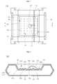
- FIG. 1 is a plan view showing a light emitting device package 100 according to a first embodiment
- FIG. 2 is a sectional view taken along line A-A of FIG. 1 .
- the light emitting device package 100 includes a package body 101, a first electrode 110, a second electrode 120, a nonconductive layer 130, a concave-convex structure 135, and a light emitting device 140.
- the package body 101 may include a conductive wafer such as a wafer level package (WLP) including silicon (Si).
- the package body 101 may include aluminum (Al), aluminum nitride (AlN), AlOx, photo sensitive glass (PSG), sapphire (Al 2 O 3 ), beryllium oxide (BeO), printed circuit board (PCB), or various resins, in addition to Si.
- Al aluminum
- AlN aluminum nitride
- AlOx aluminum oxide
- PSG photo sensitive glass
- Al 2 O 3 sapphire
- BeO beryllium oxide
- PCB printed circuit board
- the package body 101 may be etched through a bulk etching scheme as an etching process.
- a wet etching scheme, a dry etching scheme, and a laser drilling scheme may be used as the etching process. At least two among the etching schemes may be used together.
- a deep reactive ion etching scheme may be employed as the representative scheme of the dry etching scheme.
- a cavity 105 may be formed with a predetermined depth at an upper portion of the package body 101 through an etching process.
- the cavity 105 may include one of a bath tub shape recess, a polygonal recess, and a circular recess, but the embodiment is not limited thereto.
- the cavity may be formed by using wet etchants including anisotropic wet etchants such as a potassium hydroxide (KOH) solution, a Tetramethylammonium hydroxide (TMAH) solution, and an Ethylene Diamine Pyrochatechol (EDP) solution after a micro-pattern has been formed.
- KOH potassium hydroxide
- TMAH Tetramethylammonium hydroxide
- EDP Ethylene Diamine Pyrochatechol
- a lateral surface 103 of the cavity 105 in the package body 101 may be inclined at a predetermined angle or a predetermined curvature with respect to a cavity bottom surface, or may be vertically formed, but the embodiment is not limited thereto.
- An outer lateral surface 107 of the package body 101 may be inclined at a predetermined angle or may be vertically formed.
- the surface of the package body 101 is etched or cut at an angle according to the crystalline characteristic of a package body 101.
- the insulating layer 130 is formed on the surface of the package body 101.
- the insulating layer 130 may include one selected from the group consisting of silicon thermal oxides (e.g., SiO 2 and SixOy), aluminum oxide (e.g., AlOx), silicon nitrides (e.g., Si 3 N 4 , SixNy, and SiOxNy), alumina (e.g., AlN), and Al 2 O 3 .
- the insulating layer 130 insulates the package body 101 from the electrode layers 110 and 120.
- a plurality of protrusions 134 protrude from the insulating layer 130 provided on the bottom surface of the cavity 105, and the protrusions 134 protrude from the bottom surface of the cavity 105 and an opposite surface thereof while being spaced apart from each other.
- the protrusion 134 may have a side section having a lens shape, a hemispherical shape, or a dome shape.
- the protrusion 134 may have a diameter within the range of a few micrometers ( ⁇ m)(e.g. 0.1 ⁇ 9 ⁇ m), and have a height of a few micrometers ( ⁇ m) to a few tens micrometers ( ⁇ m)(e.g. 1 ⁇ 90 ⁇ m).
- the protrusion 134 may have a height lower than a top surface of the light emitting device 140.
- the protrusions 134 may include a material the same as that of the insulating layer 130.
- a photoresist layer is coated through a photolithography process, and an exposure and development process is performed to pattern a selected region such that the selected region is exposed. Therefore, the selected region is formed in the structure of a protrusion.
- the protrusions 134 of the insulating layer 130 may be formed through another scheme. According to another scheme, after providing a photoresist layer, the protrusion 134 is formed or a wet etching scheme can be performed.
- the protrusions 134 may be formed at a regular interval or an irregular interval.
- the insulating layer 130 may be deposited through a sputtering scheme or an e-beam deposition scheme, but the embodiment is not limited thereto.
- At least one well may be formed in the package body 101, and the well may be formed in the package body 101 by implanting impurities or through a diffusion process.
- the well is connected to at least one of the electrodes 110 and 120 in the structure of a circuit, and may be realized by using a protective device such as a zener diode or a constant current device.
- a plurality of electrode layers 110 and 120 may be formed on the insulating layer 130.
- the electrode layers 110 and 120 may have a stack structure of a plurality of metallic layers based on thermal conductivity, electrical characteristics, light reflection efficiency, and the manufacturing process.
- the electrode layers 110 and 120 may be formed by coating a photoresist layer on a selected region and patterning the selected region through an exposure and development process such that the selected region is exposed, thereby forming metallic layers.
- the electrode layers 110 and 120 may be formed by performing a patterning process after the metallic layers have been formed, but the embodiment is not limited thereto.
- the first electrode layer 110 may be spaced apart from the second electrode layer 120.
- the first and second electrode layers 110 and 120 may be physically separated from each other by using a separator 145.
- the separator 145 may extend from an inner part of the cavity 105 to a top surface of the package body 110.
- the separator 145 may have the form of a groove and may include an insulating material.
- the separator 145 may have various structures or various shapes, but the embodiment is not limited thereto.
- the first and second electrode layers 110 and 120 may be formed on the insulating layer 130, or may extend to one side and an opposite side of the package body 101. In addition, the first and second electrode layers 110 and 120 may extend to both sides of a bottom surface of the package body 101.
- An end portion P1 of the first electrode layer 110 and an end portion P2 of the second electrode layer 120 may be used as electrode terminals.
- the light emitting device 140 may be provided in the cavity 105.
- the light emitting device 140 may be provided on the first electrode layer 110 and/or the second electrode layer 120.
- a structure in which the light emitting device 140 is provided on the first electrode layer 110 will be described as an example.
- the same number of metallic layers may be stacked at portions of the first and second electrode layers 110 and 120.
- a region of the first electrode layer 110, to which the light emitting device 140 is bonded, serves as a bonding region, and the remaining region of the first electrode layer 110 and the second electrode layer 120 serve as a reflective region.
- a reflective metallic layer may be additionally stacked in the reflective region provided inside and outside the cavity 105.
- the difference of the stack structure may be changed according to a bonding characteristic or a reflective characteristic.
- the light emitting device 140 may be provided on a flat top surface of the first electrode layer 110.
- the region in which the light emitting device 140 is provided may serve as a bonding region.
- the light emitting device 140 may be bonded to the bonding region by using a paste (not shown) or through a die attach scheme.
- the light emitting device 140 may include an LED chip such as a blue, green, red, or yellow LED chip having a visible wavelength, or may include an LED chip in an ultraviolet (UV) band, but the embodiment is not limited to the type or the number of the light emitting devices 140.
- the light emitting device 140 may be bonded onto the first electrode layer 110 and electrically connected to the first electrode layer 110, and may be connected to the second electrode layer 120 through a wire 142.
- the light emitting device 140 may include an LED chip having a vertical type electrode structure in which electrodes are vertically provided.
- An LED chip having a lateral type electrode structure may be connected to the first and second electrode layers 110 and 120 through a wire.
- the light emitting device 140 may employ at least one of a wire, a die bonding scheme, and a flip bonding scheme, but the embodiment is not limited thereto.
- the first electrode layer 110 and the second electrode layer 120 may include at least four metallic layers.
- the bonding region of the first electrode layer 110 may include at least five metallic layers
- the reflective region may include at least one metallic layer formed on the bonding region.
- the reflective region may be formed in a region onto which light is actually incident, and the bonding region may be formed in a region excluding the reflective region.
- the first and second electrode layers 110 and 120 may have a surface roughness of about 30 nm or less (e.g., 0.01 nm to 30 nm), and such a surface roughness can improve a conductive characteristic, a heat dissipation characteristic, and light reflection efficiency.
- the first and second electrode layers 110 and 120 may have the concave-convex structure 135 by the protrusions 134 of the insulating layer 130.
- the concave-convex structure 135 is formed on the bottom surface of the cavity 105 excluding a chip mounting region in which the light emitting device 140 is mounted.
- the concave-convex structure 135 of the first and second electrode layers 110 and 120 is provided around the light emitting device 140 to scatter incident light, so that light efficiency can be improved.
- the concave-convex structure 135 includes a plurality of protrusions protruding from the electrode layers 110 and 120.
- a transmissive resin member 150 is formed in the cavity 105, and may have a single layer structure or a multiple layer structure.
- the transmissive resin member 150 seals or encapsulates the light emitting device 140, and includes resin such as silicon or epoxy.
- the transmissive resin member 150 may include at least one kind of phosphors, and the phosphors may include red, green, or yellow phosphors, but the embodiment is not limited thereof.
- the surface of the transmissive resin member 150 may have one of a concave shape, a flat shape, and convex shape.
- a lens may be formed on the cavity 105, and may include a convex lens shape, a concave lens shape, or the mixture of a convex lens shape and a concave lens shape on the transmissive resin member 150.
- the lens may be spaced apart from the transmissive resin member 150 or may make contact with the transmissive resin member 150, but the embodiment is not limited thereto.
- the lens may have various shapes, but the embodiment is not limited thereto.
- a fluorescent film including at least one kind of phosphor may be provided on the cavity 105, but the embodiment is not limited thereto.
- Silicon gel including phosphors or epoxy having superior permeability may be coated on a desired region of the transmissive resin member 150 or on a top surface of the transmissive resin member 150 through a screen printing scheme.
- the manufacturing process of the light emitting device package is as follows. After the insulating layer 130 and the first and second electrode layers 110 and 120 have been formed on the package body 101, the light emitting device 140 is electrically connected to the electrode layers 110 and 120. Then, the transmissive resin member 150 is formed in the cavity 105, and the package body 101 is cut in a package unit. The cut surface may be formed at a region excluding the first and second electrode layers 110 and 120.
- FIG. 3 is a view showing a stack structure of the first and second electrode layers of FIG. 2 .
- the first and second electrode layers 110 and 120 include a seed layer 111, a conductive layer 112, a barrier layer 113, a bonding layer 114, an adhesion layer 116, and a reflective layer 117.
- a bonding region A1 has a structure in which the seed layer 111, the conductive layer 112, the barrier layer 113, and the bonding layer 114 are sequentially stacked
- the reflective region A2 has a structure in which the seed layer 111, the conductive layer 112, the barrier layer 113, the bonding layer 114, the adhesion layer 116, and the reflective layer 117 are sequentially stacked.
- the highest layer in the bonding region A1 is the bonding layer 114, and the bonding layer 114 may be formed at the bonding region of an LED chip and at the outer portion of a package.
- the bonding layer 114 is provided in the bonding region A1, the light emitting device 140 can adhere or be bonded. Since the uppermost layer of the reflective region A2 is the reflective layer 117, the electrode layers 110 and 120 may be provided in the cavity region or at an outer peripheral portion of the cavity region.
- the bonding layer 114 and the reflective layer 117 may have surface roughness of about 30 nm or less, and, preferably, may have surface roughness of about 20 nm or less.
- the surface roughness of the bonding layer 114 may be lower than the surface roughness of the reflective layer 117.
- the seed layer 111 is deposited through a physical deposition such as a sputtering scheme or an E-beam deposition scheme.
- the conductive layer 112, the barrier layer 113, the bonding layer 114, the adhesion layer 116, and the reflective layer 117 are formed through a plating scheme (electroplating or electroless-plating).
- the seed layer 111 includes a material having higher adhesive property with the insulating layer and higher bonding property with another metal.
- the seed layer 111 includes titanium (Ti), chromium (Cr), and tantalum (Ta) in a single layer structure or a multiple layer structure.
- the seed layer 111 may have a thickness of about 900 ⁇ ⁇ 200 ⁇
- the seed layer 111 is formed in the cavity 105 of the package body 101, on a top surface of the package body 101, at a lateral surface of the package body 101, and a bottom surface of the package body 101 to effectively dissipate heat emitted from the light emitting device 140.
- An intermediate seed layer may be further formed on the seed layer 111, and may include Au or Cu. Therefore, the seed layer 111 may have a structure of Cr/Au, Cr/Cu, Ti/Au, Ta/Cu, and Ta/Ti/Cu. The intermediate seed layer may have a thickness of about 6000 ⁇ 500 ⁇ through a physical deposition scheme.
- the conductive layer 112 is formed on the seed layer 111.
- the conductive layer 112 is formed through a plating scheme, and the plating scheme reduces stress with the seed layer 111 deposited through the physical deposition scheme.
- the stress reduction can prevent the surface roughness of the conductive layer 112 from being increased. In other words, the conductive layer 112 can prevent the stress occurring due to the difference in a formation method from the seed layer 111.
- the surface roughness of the conductive layer 112 is gradually reduced to a predetermined thickness in proportion to the thickness of a plated layer.
- the conductive layer 112 may include metal, such as Cu, having higher thermal conductivity and a heat dissipation characteristic.
- the conductive layer 112 may have a thickness of a few tens ⁇ m or less, or may have a thickness of about 30 ⁇ m or less.
- the conductive layer 112 may have a thickness of 10 ⁇ m or less.
- the conductive layer may have surface roughness of 20 nm or less. If the conductive layer 112 has a thickness of 10 ⁇ m to 30 ⁇ m, a heat dissipation characteristic and surface roughness can be improved.
- the conductive layer 112 may include materials such as silver (Ag), gold (Au), and aluminum (Al) in addition to copper (Cu).
- the conductive layer 112 may include Cu-alloy or Ag-alloy.
- the barrier layer 113 may be formed on the conductive layer 112.
- the barrier layer 113 prevents the electrical characteristic of the bonding layer 114 from being reduced due to the conductive layer 112 at a high temperature.
- the barrier layer 113 may be formed through a plating scheme using platinum (Pt) or nickel (Ni), and may have a thickness of about 3000 ⁇ ⁇ 500 ⁇ .
- the bonding layer 114 is formed on the barrier layer 113.
- the bonding layer 114 may be formed through a plating scheme using gold (Au), and has a thickness of about 5000 ⁇ 500 ⁇ .
- the bonding layer 114 may have a surface roughness of about 30nm or less.
- the surface roughness of the bonding layer 114 can improve the bonding between the bonding layer 114 and the paste. As the surface roughness is increased, air is inflows into the bonded interfacial surface between the bonding layer 114 and the paste, so that thermal conductivity may be degraded. Accordingly, the surface roughness of 30 nm or less can improve the bonding property and thermal conductivity.
- the bonding region A1 may have a stack structure of Cr/Au/Cu/Ni/Au, Cr/Cu/Cu/Ni/Au, Ti/Au/Cu/Ni/Au, Ta/Cu/Cu/Ni/Au, or Ta/Ti/Cu/Cu/Ni/Au.
- the conductive layer 112 is formed at a thickness of 10 ⁇ m or less, so that the surface roughness is lowered to 30 nm or less, and the thermal resistance of the metallic layer can be lowered.
- the adhesion layer 116 and the reflective layer 117 are stacked on the bonding layer 114.
- the adhesion layer 116 is formed to bond two adjacent metallic layers to each other, and may include titanium (Ti), chromium (Cr), or tantalum (Ta).
- the adhesion layer 116 may have a thickness of 900 ⁇ 100 ⁇ . However, the adhesion layer 116 may not be formed.
- the reflective layer 117 is formed on the adhesion layer 116.
- the reflective layer 117 may include metal having superior reflectance to reflect light or alloy thereof.
- the reflective layer 117 may include Al, Ag, or alloy thereof.
- the reflective layer 117 is formed on the bottom surface and the lateral surface of the cavity 105 of FIG. 5 , so that light reflectance efficiency can be improved.
- the reflective layer 117 may have a thickness of about 1500 ⁇ 300 ⁇ .
- the conductive layer 112 reduces stress transferred from the seed layer 111, so that the surface roughness of the bonding layer 114 and the reflective layer 117 formed on the conductive layer 112 may be 30 nm or less.
- the concave-convex structure is formed to at least one part of the seed layer 111, the conductive layer 112, the barrier layer 113, the bonding layer 114, the adhesion layer 116, and a reflective layer 117.
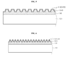
- FIG. 4 is a view showing a light emitting device package 100A according to a second embodiment.
- the second embodiment will be described with reference to FIG. 4 while focusing on the difference between the second embodiment and the first embodiment in order to avoid redundancy.
- the light emitting device package 100A includes the first concave-convex structure 135 formed at a bottom surface 102 of the cavity 105 in the package body 101, and a concave-convex structure 135A formed at a top surface 104 of the package body 101.
- a method of forming the first and second concave-convex structures 135 and 135A is considered with reference to the first embodiment.
- the first concave-convex structure 135 provided on the bottom surface of the cavity 105 scatters light emitted from the light emitting device 140 to improve light efficiency.
- the second concave-convex structure 135A provided on the top surface 104 of the package body 101 scatters light reflected by a lens, so that light extraction efficiency can be improved.
- FIGS. 5 and 6 are side sectional view showing the modified examples of a protrusion 134B of the insulating layer 130.
- the protrusion 134B of the insulating layer 130 may have a side section in a prism shape or a polygonal shape.
- the protrusion 134B may be formed through a photolithography process or a dry and/wet etching process by using the material of the insulating layer 130.
- the electrode layers 110 and 120 are formed on the insulating layer 130, thereby improving light reflection efficiency.
- a protrusion 134C of the insulating layer 130 may have a side section in a conical shape or a polygonal pyramid.
- the protrusion 134C may be formed through a photography process or a dry and/or wet etching process.
- the electrode layers 110 and 120 are formed on the insulating layer 130, thereby improving light reflective efficiency.
- Protrusions of the insulating layer 130 may have the same shape. Portions of the protrusions may have shapes different from each other, but the embodiment is not limited thereto.
- the cavity may not be formed in the package body 101.
- the insulating layer and protrusions thereof may be formed on the flat top surface, and the electrode layer may be formed on the insulating layer.
- a lighting system includes a light emitting module in which the light emitting device package of FIG. 1 is arrayed on a board in plurality.
- a light unit is provided to display apparatuses for portable terminals, notebook computers, etc., or is variously applicable to lighting apparatuses, indicator apparatuses, etc.
- the lighting system may include a display apparatus shown in FIGs. 7 and 8 , a light unit shown in FIG. 9 , in addition to a lighting lamp, a signal light, a vehicle headlight, an electronic display, etc.
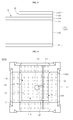
- FIG. 7 is a disassembled perspective view of a display apparatus according to an embodiment.
- the display apparatus 1000 may include a light guide panel 1041, a light emitting module 1031 supplying light to the light guide panel 1041, a reflective member 1022 under the light guide panel 1041, an optical sheet 1051 on the light guide panel 1041, a display panel 1061 on the optical sheet 1051, and a bottom cover 1011 receiving the light guide panel 1041, the light emitting module 1031, and the reflective member 1022, but the present invention is not limited thereto.
- the bottom cover 1011, the reflective sheet 1022, the light guide panel 1041, and the optical sheet 1051 may be defined as a light unit 1050.
- the light guide panel 1041 functions to transform linear light to planar light by diffusing the linear light.
- the light guide panel 1041 may be made of a transparent material, and may include one of acryl-series resin such as polymethyl metaacrylate (PMMA), polyethylene terephthlate (PET), poly carbonate (PC), Cyclic Olefin Copolymer (COC), and polyethylene naphthalate resin.
- PMMA polymethyl metaacrylate
- PET polyethylene terephthlate
- PC poly carbonate
- COC Cyclic Olefin Copolymer
- polyethylene naphthalate resin polyethylene naphthalate resin
- the light emitting module 1031 provides light to at least a side surface of the light guide panel 1041, and ultimately acts as a light source of a display apparatus.
- the light emitting module 1031 may include at least one light emitting device, and provide light directly or indirectly from one side surface of the light guide panel 1041.
- the light emitting module 1031 may include a board 1033, and a light emitting device package 100 according to embodiments disclosed above, and the light emitting device packages 100 may be arrayed apart by a predetermined interval from each other on the board 1033.
- the board 1033 may be a printed circuit board (PCB) including a circuit pattern (not shown).
- the board 1033 may include a metal core PCB (MCPCB), a flexible PCB (FPCB), etc. as well as the general PCB, but the present invention is not limited thereto.
- MCPCB metal core PCB
- FPCB flexible PCB
- the board 1033 may be removed.
- some of the heat releasing plate may contact an upper surface of the bottom cover 1011.
- the plurality of light emitting device packages 100 may be mounted on the board 1033 such that light emitting surfaces of the plurality of light emitting device packages 100 are spaced apart by a predetermined distance from the light guide panel 1041, but the present invention is not limited thereto.
- the light emitting device package 100 may supply light to a light incident part that is one side surface of the light guide panel 1041, directly or indirectly, but the present invention is not limited thereto.
- the reflective member 1022 may be provided under the light guide panel 1041.
- the reflective member 1022 reflects light incident from a lower surface of the light guide panel 1041 to allow the reflected light to be directed toward an upper direction, thereby capable of enhancing brightness of the light unit 1050.
- the reflective member 1022 may be formed of, for example, polyethylene terephthalate (PET), polycarbonate (PC), polyvinyl chloride (PVC) resin, or the like, but the present invention is not limited thereto.
- the bottom cover 1011 may receive the light guide panel 1041, the light emitting module 1031, the reflective member 1022, and the like.
- the bottom cover 1011 may have a receiving part 1012 formed in a box shape a top surface of which is opened, but the present invention is not limited thereto.
- the bottom cover 1011 may be coupled to a top cover, but the present invention is not limited thereto.
- the bottom cover 1011 may be formed of a metal material or resin material, and may be manufactured by using a process such as a press molding or an injection molding. Also, the bottom cover 1011 may include metallic or nonmetallic material having a high thermal conductivity, but the present invention is not limited thereto.
- the display panel 1061 is, for example, an LCD panel, and includes first and second transparent substrates facing each other, and a liquid crystal layer interposed between the first and second substrates.
- a polarizing plate may be attached over at least one surface of the display panel 1061, but the present invention is not limited thereto.
- the display panel 1061 displays information by using light passing through the optical sheet 1051.
- the display apparatus 1000 may be applied to a variety of mobile terminals, monitors for notebook computers, monitors for lap-top computers, televisions, etc.
- the optical sheet 1051 is disposed between the display panel 1061 and the light guide panel 1041, and includes at least one transparent sheet.
- the optical sheet 1051 may include, for example, at least one of a diffusion sheet, a horizontal and/or vertical prism sheet, and a brightness reinforcing sheet.
- the diffusion sheet diffuses incident light
- the horizontal and/or vertical prism sheet focuses incident light on a display region
- the brightness reinforcing sheet enhances the brightness by reusing lost light.
- a protective sheet may be disposed on the display panel 1061, but the present invention is not limited thereto.
- the display apparatus 1000 may include the light guide panel 1041 and the optical sheet 1051 as optical members positioned on a light path of the light emitting module 1031, but the present invention is not limited thereto.
- FIG. 8 is a cross-sectional view of a display apparatus according to an embodiment.
- the display apparatus 1100 includes a bottom cover 1152, a board 1120 on which the light emitting device packages 100 disclosed above are arrayed, an optical member 1154, and a display panel 1155.
- the board 1120 and the light emitting device package 100 may be defined as a light emitting module 1060.
- the bottom cover 1152, the at least one light emitting module 1060, and the optical member 1154 may be defined as a light unit 1150.
- the bottom cover 1152 may be provided with a receiving part 1153, but the present invention is not limited thereto.
- the optical member 1154 may include at least one of a lens, a light guide panel, a diffusion sheet, a horizontal and vertical prism sheet, and a brightness reinforcing sheet.
- the light guide panel may be formed of polycarbonate (PC) or poly methyl methacrylate (PMMA), and may be removed.
- the diffusion sheet diffuses incident light
- the horizontal and vertical prism sheet focuses incident light on a display region
- the brightness reinforcing sheet enhances the brightness by reusing lost light.
- the optical member 1154 is disposed on the light emitting module 1060.
- the optical member 1154 transforms light emitted from the light emitting module 1060 to planar light, and performs diffusion, light focusing, and the like.
- FIG. 9 is a perspective view of a lighting unit according to an embodiment.
- the lighting unit 1500 may include a case 1510, a light emitting module 1530 equipped in the case 1510, and a connection terminal 1520 equipped in the case 1510 and supplied with an electric power from an external power supply.
- the case 1510 may be preferably formed of a material having good heat shielding characteristics, for example, a metal material or a resin material.
- the light emitting module 1530 may include a board 1532, and at least one light emitting device package 100 according to the embodiments mounted on the board 1532.
- the light emitting device package 100 may include a plurality of light emitting device packages which are arrayed apart by a predetermined distance from one another in a matrix configuration.
- the board 1532 may be an insulator substrate on which a circuit pattern is printed, and may include, for example, a general printed circuit board (PCB), a metal core PCB, a flexible PCB, a ceramic PCB, an FR-4 substrate, etc.
- PCB general printed circuit board
- the board 1532 may be formed of a material to efficiently reflect light, and a surface thereof may be formed in a color capable of efficiently reflecting light, for example, white color, or silver color.
- the at least one light emitting device packages 100 may be mounted on the board 1532.
- Each of the light emitting device packages 100 may include at least one light emitting diode (LED) chip.
- the LED chip may include a color LED emitting red, green, blue or white light, and a UV LED emitting ultraviolet (UV).
- the light emitting module 1530 may have a combination of various light emitting device packages so as to obtain desired color and luminance.
- the light emitting module 1530 may have a combination of a white LED, a red LED, and a green LED so as to obtain a high color rendering index (CRI).
- CRI color rendering index
- connection terminal 1520 may be electrically connected to the light emitting module 1530 to supply power.
- the connection terminal 1520 may be screwed and coupled to an external power in a socket type, but the present invention is not limited thereto.
- the connection terminal 1520 may be made in a pin type and inserted into an external power, or may be connected to the external power through a power line.
- a light emitting module of a light unit includes the light emitting device package.
- the light emitting device package may have the above disclosed package structure.
- the resultant structure is packaged by using a molding member.
- a method of manufacturing a light emitting device package includes steps of forming an insulating layer on a surface of a package body, forming a plurality of protrusions in a first region of the insulating layer, forming a plurality of metallic layers on the insulating layer, and connecting the light emitting device with the metallic layers.
- any reference in this specification to "one embodiment,” “an embodiment,” “example embodiment,” etc. means that a particular feature, structure, or characteristic described in connection with the embodiment is included in at least one embodiment of the invention.
- the appearances of such phrases in various places in the specification are not necessarily all referring to the same embodiment.
Landscapes
- Engineering & Computer Science (AREA)
- Microelectronics & Electronic Packaging (AREA)
- Manufacturing & Machinery (AREA)
- Computer Hardware Design (AREA)
- Power Engineering (AREA)
- Led Device Packages (AREA)
Applications Claiming Priority (1)
| Application Number | Priority Date | Filing Date | Title |
|---|---|---|---|
| KR1020100005199A KR101091304B1 (ko) | 2010-01-20 | 2010-01-20 | 발광 소자 패키지 및 그 제조방법 |
Publications (3)
| Publication Number | Publication Date |
|---|---|
| EP2348552A2 true EP2348552A2 (de) | 2011-07-27 |
| EP2348552A3 EP2348552A3 (de) | 2012-07-04 |
| EP2348552B1 EP2348552B1 (de) | 2016-06-01 |
Family
ID=43836864
Family Applications (1)
| Application Number | Title | Priority Date | Filing Date |
|---|---|---|---|
| EP10179455.0A Active EP2348552B1 (de) | 2010-01-20 | 2010-09-24 | Lichtemittierendes Vorrichtungsgehäuse und Lichteinheit damit |
Country Status (5)
| Country | Link |
|---|---|
| US (1) | US8395170B2 (de) |
| EP (1) | EP2348552B1 (de) |
| KR (1) | KR101091304B1 (de) |
| CN (1) | CN102130272B (de) |
| TW (1) | TWI520380B (de) |
Cited By (2)
| Publication number | Priority date | Publication date | Assignee | Title |
|---|---|---|---|---|
| EP2562831A3 (de) * | 2011-08-24 | 2015-04-08 | LG Innotek Co., Ltd. | Gehäuse für eine lichtemittierende Vorrichtung und Beleuchtungssystem |
| EP2860773A4 (de) * | 2012-06-08 | 2015-07-29 | Lg Innotek Co Ltd | Lichtemittierende vorrichtung, verkapselung für lichtemittierende vorrichtung und beleuchtungseinheit |
Families Citing this family (17)
| Publication number | Priority date | Publication date | Assignee | Title |
|---|---|---|---|---|
| KR101072212B1 (ko) * | 2010-01-05 | 2011-10-10 | 엘지이노텍 주식회사 | 발광 소자 및 그 제조방법 |
| KR101028329B1 (ko) * | 2010-04-28 | 2011-04-12 | 엘지이노텍 주식회사 | 발광 소자 패키지 및 그 제조방법 |
| KR20130035658A (ko) | 2011-09-30 | 2013-04-09 | 서울옵토디바이스주식회사 | 발광 다이오드 소자용 기판 제조 방법 |
| KR20140094752A (ko) | 2013-01-22 | 2014-07-31 | 삼성전자주식회사 | 전자소자 패키지 및 이에 사용되는 패키지 기판 |
| US20140209950A1 (en) * | 2013-01-31 | 2014-07-31 | Luxo-Led Co., Limited | Light emitting diode package module |
| US10278243B2 (en) | 2014-03-06 | 2019-04-30 | Seoul Semiconductor Co., Ltd. | Backlight module with MJT LED and backlight unit including the same |
| KR102364160B1 (ko) * | 2014-03-06 | 2022-02-21 | 서울반도체 주식회사 | Mjt led를 이용한 백라이트 모듈 및 이를 포함하는 백라이트 유닛 |
| KR20170058489A (ko) * | 2015-11-18 | 2017-05-29 | 주식회사 세미콘라이트 | 반도체 발광소자용 프레임 |
| US9842977B2 (en) * | 2016-06-08 | 2017-12-12 | Raul A. Klein | Circuit board and method of manufacture |
| US20170084810A1 (en) * | 2016-12-05 | 2017-03-23 | Raul A. Klein | Thermally Conductive Circuit Board Substrate and Method of Manufacture |
| CN107045992A (zh) * | 2017-04-19 | 2017-08-15 | 中国科学院上海微系统与信息技术研究所 | 图像传感器圆片级封装方法及封装结构 |
| KR102515673B1 (ko) * | 2017-11-09 | 2023-03-30 | 쑤저우 레킨 세미컨덕터 컴퍼니 리미티드 | 조명 장치 |
| KR102435409B1 (ko) | 2018-01-04 | 2022-08-24 | 엘지전자 주식회사 | 반도체 발광소자를 이용한 디스플레이 장치 |
| KR20190086300A (ko) | 2018-01-12 | 2019-07-22 | 엘지이노텍 주식회사 | 조명 모듈 및 이를 구비한 조명 장치 |
| CN111968964B (zh) * | 2020-04-27 | 2022-03-29 | 深圳赛曼智能照明科技有限公司 | 一种led照明灯及其制造方法 |
| CN112038332B (zh) * | 2020-04-27 | 2022-04-12 | 江门市品而亮照明有限公司 | 一种led灯带及其制造方法 |
| KR20220060007A (ko) * | 2020-11-02 | 2022-05-11 | 삼성디스플레이 주식회사 | 발광 소자 잉크, 표시 장치 및 그 제조 방법 |
Family Cites Families (17)
| Publication number | Priority date | Publication date | Assignee | Title |
|---|---|---|---|---|
| KR100214463B1 (ko) * | 1995-12-06 | 1999-08-02 | 구본준 | 클립형 리드프레임과 이를 사용한 패키지의 제조방법 |
| US20030075724A1 (en) * | 2001-10-19 | 2003-04-24 | Bily Wang | Wing-shaped surface mount package for light emitting diodes |
| US7795623B2 (en) * | 2004-06-30 | 2010-09-14 | Cree, Inc. | Light emitting devices having current reducing structures and methods of forming light emitting devices having current reducing structures |
| JP2006086176A (ja) * | 2004-09-14 | 2006-03-30 | Hitachi Kyowa Engineering Co Ltd | Led用サブマウント及びその製造方法 |
| JP4176703B2 (ja) * | 2004-11-25 | 2008-11-05 | 松下電器産業株式会社 | 半導体発光装置、照明装置、携帯通信機器、カメラ、及び製造方法 |
| KR100862515B1 (ko) | 2005-09-23 | 2008-10-08 | 삼성전기주식회사 | 발광소자 패키지 |
| KR100678860B1 (ko) | 2005-11-10 | 2007-02-05 | 전자부품연구원 | 전극 패턴 형성방법 |
| JP5091421B2 (ja) * | 2006-04-07 | 2012-12-05 | 株式会社東芝 | 半導体発光装置 |
| KR100854328B1 (ko) | 2006-07-07 | 2008-08-28 | 엘지전자 주식회사 | 발광 소자 패키지 및 그 제조방법 |
| CN101123286A (zh) | 2006-08-09 | 2008-02-13 | 刘胜 | 发光二极管封装结构和方法 |
| JP2008053685A (ja) * | 2006-08-23 | 2008-03-06 | Samsung Electro Mech Co Ltd | 垂直構造窒化ガリウム系発光ダイオード素子及びその製造方法 |
| JP5154819B2 (ja) * | 2007-04-03 | 2013-02-27 | 新光電気工業株式会社 | 基板及びその製造方法 |
| KR101283282B1 (ko) | 2007-07-25 | 2013-07-11 | 엘지이노텍 주식회사 | 발광 소자 패키지 및 그 제조방법 |
| KR100877881B1 (ko) * | 2007-09-06 | 2009-01-08 | 엘지이노텍 주식회사 | 발광다이오드 패키지 및 그 제조방법 |
| US7923746B2 (en) * | 2008-03-12 | 2011-04-12 | Industrial Technology Research Institute | Light emitting diode package structure and method for fabricating the same |
| KR100992778B1 (ko) * | 2008-05-23 | 2010-11-05 | 엘지이노텍 주식회사 | 발광소자 패키지 및 그 제조방법 |
| CN201307605Y (zh) | 2008-12-05 | 2009-09-09 | 弘凯光电(深圳)有限公司 | Led封装结构 |
-
2010
- 2010-01-20 KR KR1020100005199A patent/KR101091304B1/ko active IP Right Grant
- 2010-09-13 US US12/880,683 patent/US8395170B2/en active Active
- 2010-09-24 EP EP10179455.0A patent/EP2348552B1/de active Active
- 2010-10-13 TW TW099134878A patent/TWI520380B/zh active
- 2010-10-15 CN CN201010513392.3A patent/CN102130272B/zh active Active
Non-Patent Citations (1)
| Title |
|---|
| None |
Cited By (3)
| Publication number | Priority date | Publication date | Assignee | Title |
|---|---|---|---|---|
| EP2562831A3 (de) * | 2011-08-24 | 2015-04-08 | LG Innotek Co., Ltd. | Gehäuse für eine lichtemittierende Vorrichtung und Beleuchtungssystem |
| EP2860773A4 (de) * | 2012-06-08 | 2015-07-29 | Lg Innotek Co Ltd | Lichtemittierende vorrichtung, verkapselung für lichtemittierende vorrichtung und beleuchtungseinheit |
| US9450146B2 (en) | 2012-06-08 | 2016-09-20 | Lg Innotek Co., Ltd. | Light-emitting device, light-emitting device package, and light unit |
Also Published As
| Publication number | Publication date |
|---|---|
| TWI520380B (zh) | 2016-02-01 |
| US20110175122A1 (en) | 2011-07-21 |
| CN102130272A (zh) | 2011-07-20 |
| EP2348552A3 (de) | 2012-07-04 |
| KR101091304B1 (ko) | 2011-12-07 |
| CN102130272B (zh) | 2014-04-30 |
| EP2348552B1 (de) | 2016-06-01 |
| US8395170B2 (en) | 2013-03-12 |
| TW201126767A (en) | 2011-08-01 |
| KR20110085421A (ko) | 2011-07-27 |
Similar Documents
| Publication | Publication Date | Title |
|---|---|---|
| EP2348552B1 (de) | Lichtemittierendes Vorrichtungsgehäuse und Lichteinheit damit | |
| EP2365550B1 (de) | Gehäuse für Leuchtdiode | |
| KR101028329B1 (ko) | 발광 소자 패키지 및 그 제조방법 | |
| US8860072B2 (en) | Light emitting device and light unit having the same | |
| US7264378B2 (en) | Power surface mount light emitting die package | |
| US20140284643A1 (en) | Power surface mount light emitting die package | |
| US8357948B2 (en) | Light emitting device and lighting system | |
| KR20120015415A (ko) | 발광 소자 및 이를 구비한 조명 시스템 | |
| KR101047633B1 (ko) | 발광소자 및 이를 구비한 라이트 유닛 | |
| KR20110138756A (ko) | 발광 소자 | |
| KR101924014B1 (ko) | 발광 소자 패키지 및 이를 구비한 조명 시스템 | |
| KR101628381B1 (ko) | 발광 소자 패키지 및 그 제조방법 | |
| KR20140076879A (ko) | 발광소자 패키지 | |
| KR20110138757A (ko) | 발광 소자 | |
| KR20120087581A (ko) | 발광소자 패키지 | |
| KR20120099549A (ko) | 발광 소자 패키지, 발광 소자 패키지 제조방법 및 조명 시스템 | |
| KR20140096849A (ko) | 발광소자 패키지 | |
| KR20120136043A (ko) | 발광소자 패키지 |
Legal Events
| Date | Code | Title | Description |
|---|---|---|---|
| PUAI | Public reference made under article 153(3) epc to a published international application that has entered the european phase |
Free format text: ORIGINAL CODE: 0009012 |
|
| 17P | Request for examination filed |
Effective date: 20100924 |
|
| AK | Designated contracting states |
Kind code of ref document: A2 Designated state(s): AL AT BE BG CH CY CZ DE DK EE ES FI FR GB GR HR HU IE IS IT LI LT LU LV MC MK MT NL NO PL PT RO SE SI SK SM TR |
|
| AX | Request for extension of the european patent |
Extension state: BA ME RS |
|
| PUAL | Search report despatched |
Free format text: ORIGINAL CODE: 0009013 |
|
| AK | Designated contracting states |
Kind code of ref document: A3 Designated state(s): AL AT BE BG CH CY CZ DE DK EE ES FI FR GB GR HR HU IE IS IT LI LT LU LV MC MK MT NL NO PL PT RO SE SI SK SM TR |
|
| AX | Request for extension of the european patent |
Extension state: BA ME RS |
|
| RIC1 | Information provided on ipc code assigned before grant |
Ipc: H01L 33/48 20100101ALN20120531BHEP Ipc: H01L 33/52 20100101ALN20120531BHEP Ipc: H01L 33/60 20100101ALI20120531BHEP Ipc: H01L 33/62 20100101AFI20120531BHEP Ipc: H01L 33/64 20100101ALN20120531BHEP |
|
| 17Q | First examination report despatched |
Effective date: 20130514 |
|
| RAP1 | Party data changed (applicant data changed or rights of an application transferred) |
Owner name: LG INNOTEK CO., LTD. |
|
| GRAP | Despatch of communication of intention to grant a patent |
Free format text: ORIGINAL CODE: EPIDOSNIGR1 |
|
| INTG | Intention to grant announced |
Effective date: 20151222 |
|
| RIC1 | Information provided on ipc code assigned before grant |
Ipc: H01L 33/64 20100101ALN20151211BHEP Ipc: H01L 33/60 20100101ALI20151211BHEP Ipc: H01L 33/62 20100101AFI20151211BHEP Ipc: H01L 33/52 20100101ALN20151211BHEP Ipc: H01L 33/48 20100101ALN20151211BHEP |
|
| GRAS | Grant fee paid |
Free format text: ORIGINAL CODE: EPIDOSNIGR3 |
|
| GRAA | (expected) grant |
Free format text: ORIGINAL CODE: 0009210 |
|
| AK | Designated contracting states |
Kind code of ref document: B1 Designated state(s): AL AT BE BG CH CY CZ DE DK EE ES FI FR GB GR HR HU IE IS IT LI LT LU LV MC MK MT NL NO PL PT RO SE SI SK SM TR |
|
| REG | Reference to a national code |
Ref country code: GB Ref legal event code: FG4D |
|
| REG | Reference to a national code |
Ref country code: AT Ref legal event code: REF Ref document number: 804346 Country of ref document: AT Kind code of ref document: T Effective date: 20160615 Ref country code: CH Ref legal event code: EP |
|
| REG | Reference to a national code |
Ref country code: IE Ref legal event code: FG4D |
|
| REG | Reference to a national code |
Ref country code: DE Ref legal event code: R096 Ref document number: 602010033748 Country of ref document: DE |
|
| REG | Reference to a national code |
Ref country code: FR Ref legal event code: PLFP Year of fee payment: 7 |
|
| REG | Reference to a national code |
Ref country code: NL Ref legal event code: FP |
|
| REG | Reference to a national code |
Ref country code: LT Ref legal event code: MG4D |
|
| PG25 | Lapsed in a contracting state [announced via postgrant information from national office to epo] |
Ref country code: LT Free format text: LAPSE BECAUSE OF FAILURE TO SUBMIT A TRANSLATION OF THE DESCRIPTION OR TO PAY THE FEE WITHIN THE PRESCRIBED TIME-LIMIT Effective date: 20160601 Ref country code: FI Free format text: LAPSE BECAUSE OF FAILURE TO SUBMIT A TRANSLATION OF THE DESCRIPTION OR TO PAY THE FEE WITHIN THE PRESCRIBED TIME-LIMIT Effective date: 20160601 Ref country code: NO Free format text: LAPSE BECAUSE OF FAILURE TO SUBMIT A TRANSLATION OF THE DESCRIPTION OR TO PAY THE FEE WITHIN THE PRESCRIBED TIME-LIMIT Effective date: 20160901 |
|
| REG | Reference to a national code |
Ref country code: AT Ref legal event code: MK05 Ref document number: 804346 Country of ref document: AT Kind code of ref document: T Effective date: 20160601 |
|
| PG25 | Lapsed in a contracting state [announced via postgrant information from national office to epo] |
Ref country code: SE Free format text: LAPSE BECAUSE OF FAILURE TO SUBMIT A TRANSLATION OF THE DESCRIPTION OR TO PAY THE FEE WITHIN THE PRESCRIBED TIME-LIMIT Effective date: 20160601 Ref country code: LV Free format text: LAPSE BECAUSE OF FAILURE TO SUBMIT A TRANSLATION OF THE DESCRIPTION OR TO PAY THE FEE WITHIN THE PRESCRIBED TIME-LIMIT Effective date: 20160601 Ref country code: GR Free format text: LAPSE BECAUSE OF FAILURE TO SUBMIT A TRANSLATION OF THE DESCRIPTION OR TO PAY THE FEE WITHIN THE PRESCRIBED TIME-LIMIT Effective date: 20160902 Ref country code: HR Free format text: LAPSE BECAUSE OF FAILURE TO SUBMIT A TRANSLATION OF THE DESCRIPTION OR TO PAY THE FEE WITHIN THE PRESCRIBED TIME-LIMIT Effective date: 20160601 Ref country code: ES Free format text: LAPSE BECAUSE OF FAILURE TO SUBMIT A TRANSLATION OF THE DESCRIPTION OR TO PAY THE FEE WITHIN THE PRESCRIBED TIME-LIMIT Effective date: 20160601 |
|
| PG25 | Lapsed in a contracting state [announced via postgrant information from national office to epo] |
Ref country code: IT Free format text: LAPSE BECAUSE OF FAILURE TO SUBMIT A TRANSLATION OF THE DESCRIPTION OR TO PAY THE FEE WITHIN THE PRESCRIBED TIME-LIMIT Effective date: 20160601 Ref country code: IS Free format text: LAPSE BECAUSE OF FAILURE TO SUBMIT A TRANSLATION OF THE DESCRIPTION OR TO PAY THE FEE WITHIN THE PRESCRIBED TIME-LIMIT Effective date: 20161001 Ref country code: SK Free format text: LAPSE BECAUSE OF FAILURE TO SUBMIT A TRANSLATION OF THE DESCRIPTION OR TO PAY THE FEE WITHIN THE PRESCRIBED TIME-LIMIT Effective date: 20160601 Ref country code: RO Free format text: LAPSE BECAUSE OF FAILURE TO SUBMIT A TRANSLATION OF THE DESCRIPTION OR TO PAY THE FEE WITHIN THE PRESCRIBED TIME-LIMIT Effective date: 20160601 Ref country code: EE Free format text: LAPSE BECAUSE OF FAILURE TO SUBMIT A TRANSLATION OF THE DESCRIPTION OR TO PAY THE FEE WITHIN THE PRESCRIBED TIME-LIMIT Effective date: 20160601 Ref country code: CZ Free format text: LAPSE BECAUSE OF FAILURE TO SUBMIT A TRANSLATION OF THE DESCRIPTION OR TO PAY THE FEE WITHIN THE PRESCRIBED TIME-LIMIT Effective date: 20160601 |
|
| PG25 | Lapsed in a contracting state [announced via postgrant information from national office to epo] |
Ref country code: BE Free format text: LAPSE BECAUSE OF NON-PAYMENT OF DUE FEES Effective date: 20160601 Ref country code: AT Free format text: LAPSE BECAUSE OF FAILURE TO SUBMIT A TRANSLATION OF THE DESCRIPTION OR TO PAY THE FEE WITHIN THE PRESCRIBED TIME-LIMIT Effective date: 20160601 Ref country code: SM Free format text: LAPSE BECAUSE OF FAILURE TO SUBMIT A TRANSLATION OF THE DESCRIPTION OR TO PAY THE FEE WITHIN THE PRESCRIBED TIME-LIMIT Effective date: 20160601 Ref country code: PL Free format text: LAPSE BECAUSE OF FAILURE TO SUBMIT A TRANSLATION OF THE DESCRIPTION OR TO PAY THE FEE WITHIN THE PRESCRIBED TIME-LIMIT Effective date: 20160601 Ref country code: PT Free format text: LAPSE BECAUSE OF FAILURE TO SUBMIT A TRANSLATION OF THE DESCRIPTION OR TO PAY THE FEE WITHIN THE PRESCRIBED TIME-LIMIT Effective date: 20161003 |
|
| REG | Reference to a national code |
Ref country code: DE Ref legal event code: R097 Ref document number: 602010033748 Country of ref document: DE |
|
| PLBE | No opposition filed within time limit |
Free format text: ORIGINAL CODE: 0009261 |
|
| STAA | Information on the status of an ep patent application or granted ep patent |
Free format text: STATUS: NO OPPOSITION FILED WITHIN TIME LIMIT |
|
| PG25 | Lapsed in a contracting state [announced via postgrant information from national office to epo] |
Ref country code: MC Free format text: LAPSE BECAUSE OF FAILURE TO SUBMIT A TRANSLATION OF THE DESCRIPTION OR TO PAY THE FEE WITHIN THE PRESCRIBED TIME-LIMIT Effective date: 20160601 |
|
| REG | Reference to a national code |
Ref country code: CH Ref legal event code: PL |
|
| 26N | No opposition filed |
Effective date: 20170302 |
|
| GBPC | Gb: european patent ceased through non-payment of renewal fee |
Effective date: 20160924 |
|
| PG25 | Lapsed in a contracting state [announced via postgrant information from national office to epo] |
Ref country code: SI Free format text: LAPSE BECAUSE OF FAILURE TO SUBMIT A TRANSLATION OF THE DESCRIPTION OR TO PAY THE FEE WITHIN THE PRESCRIBED TIME-LIMIT Effective date: 20160601 Ref country code: DK Free format text: LAPSE BECAUSE OF FAILURE TO SUBMIT A TRANSLATION OF THE DESCRIPTION OR TO PAY THE FEE WITHIN THE PRESCRIBED TIME-LIMIT Effective date: 20160601 |
|
| REG | Reference to a national code |
Ref country code: IE Ref legal event code: MM4A |
|
| PG25 | Lapsed in a contracting state [announced via postgrant information from national office to epo] |
Ref country code: LI Free format text: LAPSE BECAUSE OF NON-PAYMENT OF DUE FEES Effective date: 20160930 Ref country code: GB Free format text: LAPSE BECAUSE OF NON-PAYMENT OF DUE FEES Effective date: 20160924 Ref country code: CH Free format text: LAPSE BECAUSE OF NON-PAYMENT OF DUE FEES Effective date: 20160930 Ref country code: IE Free format text: LAPSE BECAUSE OF NON-PAYMENT OF DUE FEES Effective date: 20160924 |
|
| REG | Reference to a national code |
Ref country code: FR Ref legal event code: PLFP Year of fee payment: 8 |
|
| PG25 | Lapsed in a contracting state [announced via postgrant information from national office to epo] |
Ref country code: LU Free format text: LAPSE BECAUSE OF NON-PAYMENT OF DUE FEES Effective date: 20160924 |
|
| PG25 | Lapsed in a contracting state [announced via postgrant information from national office to epo] |
Ref country code: HU Free format text: LAPSE BECAUSE OF FAILURE TO SUBMIT A TRANSLATION OF THE DESCRIPTION OR TO PAY THE FEE WITHIN THE PRESCRIBED TIME-LIMIT; INVALID AB INITIO Effective date: 20100924 Ref country code: CY Free format text: LAPSE BECAUSE OF FAILURE TO SUBMIT A TRANSLATION OF THE DESCRIPTION OR TO PAY THE FEE WITHIN THE PRESCRIBED TIME-LIMIT Effective date: 20160601 |
|
| PG25 | Lapsed in a contracting state [announced via postgrant information from national office to epo] |
Ref country code: MT Free format text: LAPSE BECAUSE OF NON-PAYMENT OF DUE FEES Effective date: 20160930 Ref country code: TR Free format text: LAPSE BECAUSE OF FAILURE TO SUBMIT A TRANSLATION OF THE DESCRIPTION OR TO PAY THE FEE WITHIN THE PRESCRIBED TIME-LIMIT Effective date: 20160601 Ref country code: MK Free format text: LAPSE BECAUSE OF FAILURE TO SUBMIT A TRANSLATION OF THE DESCRIPTION OR TO PAY THE FEE WITHIN THE PRESCRIBED TIME-LIMIT Effective date: 20160601 |
|
| PG25 | Lapsed in a contracting state [announced via postgrant information from national office to epo] |
Ref country code: BG Free format text: LAPSE BECAUSE OF FAILURE TO SUBMIT A TRANSLATION OF THE DESCRIPTION OR TO PAY THE FEE WITHIN THE PRESCRIBED TIME-LIMIT Effective date: 20160601 |
|
| REG | Reference to a national code |
Ref country code: FR Ref legal event code: PLFP Year of fee payment: 9 |
|
| PG25 | Lapsed in a contracting state [announced via postgrant information from national office to epo] |
Ref country code: AL Free format text: LAPSE BECAUSE OF FAILURE TO SUBMIT A TRANSLATION OF THE DESCRIPTION OR TO PAY THE FEE WITHIN THE PRESCRIBED TIME-LIMIT Effective date: 20160601 |
|
| REG | Reference to a national code |
Ref country code: NL Ref legal event code: PD Owner name: SUZHOU LEKIN SEMICONDUCTOR CO., LTD.; CN Free format text: DETAILS ASSIGNMENT: CHANGE OF OWNER(S), ASSIGNMENT; FORMER OWNER NAME: LG INNOTEK CO., LTD. Effective date: 20210719 |
|
| REG | Reference to a national code |
Ref country code: DE Ref legal event code: R081 Ref document number: 602010033748 Country of ref document: DE Owner name: SUZHOU LEKIN SEMICONDUCTOR CO. LTD., TAICANG, CN Free format text: FORMER OWNER: LG INNOTEK CO., LTD., SEOUL, KR |
|
| PGFP | Annual fee paid to national office [announced via postgrant information from national office to epo] |
Ref country code: NL Payment date: 20230816 Year of fee payment: 14 |
|
| PGFP | Annual fee paid to national office [announced via postgrant information from national office to epo] |
Ref country code: FR Payment date: 20230808 Year of fee payment: 14 Ref country code: DE Payment date: 20230808 Year of fee payment: 14 |