EP2347909B1 - Driver circuit, driver apparatus, and image forming apparatus - Google Patents
Driver circuit, driver apparatus, and image forming apparatus Download PDFInfo
- Publication number
- EP2347909B1 EP2347909B1 EP11151263.8A EP11151263A EP2347909B1 EP 2347909 B1 EP2347909 B1 EP 2347909B1 EP 11151263 A EP11151263 A EP 11151263A EP 2347909 B1 EP2347909 B1 EP 2347909B1
- Authority
- EP
- European Patent Office
- Prior art keywords
- terminal
- light emitting
- circuit
- switch
- current
- Prior art date
- Legal status (The legal status is an assumption and is not a legal conclusion. Google has not performed a legal analysis and makes no representation as to the accuracy of the status listed.)
- Not-in-force
Links
Images


Classifications
-
- B—PERFORMING OPERATIONS; TRANSPORTING
- B41—PRINTING; LINING MACHINES; TYPEWRITERS; STAMPS
- B41J—TYPEWRITERS; SELECTIVE PRINTING MECHANISMS, i.e. MECHANISMS PRINTING OTHERWISE THAN FROM A FORME; CORRECTION OF TYPOGRAPHICAL ERRORS
- B41J2/00—Typewriters or selective printing mechanisms characterised by the printing or marking process for which they are designed
- B41J2/435—Typewriters or selective printing mechanisms characterised by the printing or marking process for which they are designed characterised by selective application of radiation to a printing material or impression-transfer material
- B41J2/447—Typewriters or selective printing mechanisms characterised by the printing or marking process for which they are designed characterised by selective application of radiation to a printing material or impression-transfer material using arrays of radiation sources
- B41J2/45—Typewriters or selective printing mechanisms characterised by the printing or marking process for which they are designed characterised by selective application of radiation to a printing material or impression-transfer material using arrays of radiation sources using light-emitting diode [LED] or laser arrays
Definitions
- the print head includes light emitting arrays and a self-scanning circuit.
- the light emitting array includes a plurality of light emitting thyristors that have an anode connected to a power supply and a cathode connected to a ground terminal.
- the self-scanning circuit provides a trigger signal to the gates of the respective light emitting thyristors.
- the driver circuit is constituted of CMOS inverters formed of CMOS transistors and current limiting resistors connected to the output of the CMOS inverters. The current limiting resistors are connected to the common terminal through the cable.
- the above-described self-scanning print head operates as follows: Forward voltage is supplied to the light emitting thyristors through the current limiting resistors to a common terminal to which the anodes of the light emitting thyristors are connected.
- the self-scanning circuit provides a trigger signal to the gate of a corresponding light emitting thyristor to emit light, thereby causing the light emitting thyristor to emit light.
- One way of alleviating the signal reflection is to select a cable having a characteristic impedance that matches the resistance of the current limiting resistor.
- cables on the market have their predetermined characteristic impedances and cannot be selected to meet individual circuit designs.
- the resistance of the current limiting resistor is selected in accordance with the supply voltage of the CMOS inverter and the anode-cathode voltage and drive current of the light emitting thyristor, and is about 200 ohms.
- the resistance of the current limiting resistor necessarily differs from the characteristic impedance of the cable, so that signal reflection occurs due impedance mismatching between the cable and the current limiting resistor. This leads to the problem of accurately controlling the amount of exposure energy.
- An object of the invention is to solve the aforementioned prior art problems.
- a driving circuit is used for driving a plurality of groups of switch elements connected between a power supply terminal (VDD) and a common terminal (IN).
- Each switch element includes an anode connected to the power supply terminal (VDD), a cathode, and a gate.
- the anode is connected to the power supply and the cathode connected to a common terminal.
- the gate controls electrical conduction between the anode and the cathode.
- the driving circuit includes a power supply terminal (VDD), a common terminal (IN) and a said group comprising a plurality of switch elements.
- the driving circuit includes a switch circuit connected between the power supply terminal and the common terminal, and a driver circuit (41, 42, 43) into which drive current (Iout) flows.
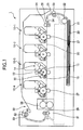
- the image forming apparatus 1 is a tandem electrophotographic color printer incorporating a print head e.g., an optical print head that employs a driver apparatus for driving arrays of light emitting elements, e.g., three-terminal thyristors.
- the image forming apparatus 1 includes four process units 10-1 to 10-4 that form a black (K), a yellow (Y) image, a magenta (M) image, and a cyan (C) image, respectively.
- the four process units are aligned from upstream to downstream of the transport path of a recording medium, e.g., paper 20.
- Each of the process units may be substantially identical; for simplicity only the operation of the process unit 10-3 for forming cyan images will be described, it being understood that the other process units may work in a similar fashion.
- the process unit 10-3 includes a photoconductive drum 11 rotatable in a direction shown by arrow A.
- a charging unit 12, an exposing unit, e.g., an optical print head 13, a developing unit 14, and a cleaning device 15 are disposed in this order around the photoconductive drum 11.
- the charging unit 12 charges the surface of the photoconductive drum 11.
- the exposing unit 13 selectively illuminates the charged surface of the photoconductive drum 11 to form an electrostatic latent image.
- the developing unit 14 deposits magenta toner to the electrostatic latent image formed on the photoconductive drum 11 to form a magenta toner image.
- the cleaning device 15 removes toner remaining on the photoconductive drum 11 after transferring the magenta toner image onto the paper 20.
- a drive source (not shown) drives the photoconductive drum 11 and a variety of rollers in rotation via a gear train.
- a hopping roller 22 is disposed over the paper cassette 21, and feeds the paper 20 on a sheet-by-sheet basis into the transport path.
- a transport roller 25 cooperates with a pinch roller 24 to hold the paper 20 in a sandwiched relation.
- a registry roller 26 cooperates with a pinch roller 24 to correct the skew of the paper 20, and transports the paper 20 to the process unit 10-1.
- the transport roller 25 and registry roller 26 are disposed downstream of the hopping roller 22.
- a drive source (not shown) drives the hopping roller 22, transport roller 25, and registry roller 26 in rotation via a gear train.
- a fixing unit 28 is located downstream of the process unit 10-4, and includes a heat roller, which incorporates a heater therein, and a pressure roller.
- a heat roller which incorporates a heater therein
- a pressure roller When the paper 20 passes through a fixing point defined between the pressure roller and the heat roller, the toner image on the paper 20 is fixed under heat and pressure.
- Discharge rollers 29 and 30, pinch rollers 31 and 32, and a paper stacker 33 are disposed downstream of the fixing unit 28.
- the discharge rollers 29 and 30 cooperate with the pressure rollers 31 and 32, respectively, to hold the paper 20 in a sandwiched relation, and transport the paper 20 to the paper stacker 33.
- the heat roller, pressure roller, and discharge rollers 29 and 30 are driven in rotation by a drive power transmitted from a drive source (not shown) via, for example, a gear train.
- the image forming apparatus 1 operates as follows:
- the hopping roller 22 feeds the paper 20 into the transport path from the paper cassette 21 on a sheet-by-sheet basis.
- the paper 20 is held by the transport roller 25, registry roller 26, and pinch rollers 23 and 24 in a sandwiched relation, and is transported into a transfer point defined between the photoconductive drum 11 of the process unit 10-1 and the transfer unit 27.
- the photoconductive drum 11 rotates, the paper 20 is further transported through the transfer point so that the toner image on the photoconductive drum 11 is transferred onto the paper 20.
- the paper 20 is transported through the remaining process units 10-2 to 10-4 so that the toner images of corresponding colors are transferred onto the paper 20 in registration,
- the toner images carried on the paper 20 are fixed.
- the paper 20 is further transported by the discharge rollers 29 and 30 and pinch rollers 31 and 32 to the paper stacker 33 defined on the outer wall of the image forming apparatus 1. This completes printing.
- Fig. 2 is a cross-sectional view of the optical print head 13 shown in Fig. 1 .
- Fig. 3 is a perspective view of a circuit board 13b shown in Fig. 2 .
- a lens array 13c (e.g., rod lens array) is constituted of a plurality of column-shaped optical elements and is disposed above a plurality of light emitting arrays 200.
- the rod lens array 13c is fixedly supported by a holder 13d.
- the base 13a, printed circuit board 13b, and holder 13d are clamped firmly together by means of clamp members 13e and 13f.
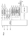
- Fig. 4 is a block diagram illustrating the configuration of a printer controller for use with the image forming apparatus 1 shown in Fig. 1 .
- the printer controller includes a printing controller 40 located in a print engine of the image forming apparatus 1.
- the printing controller 40 mainly includes a microprocessor, a read only memory (ROM), a random access memory (RAM), an input/output port, and a timer.
- the printer controller receives a control signal SG1 and a video signal (bit map data) SG2 from an image processing section (not shown) to perform sequential control of the overall operation of the image forming apparatus 1, thereby performing printing.
- the printing controller 40 is connected to the four optical print heads 13 of the process units 10-1 to 10-4, a heater 28a of the fixing unit 28, drivers 50 and 52, an incoming paper sensor 54, an outgoing paper sensor 55, a remaining paper sensor 56, a paper size sensor 57, a fixing unit temperature sensor 58, a high voltage charging power supply 59, and a high voltage transferring power supply 60.
- the driver 50 is connected to a developing/transferring process motor (PM) 51.
- the driver 52 is connected to a paper transporting motor (PM) 53.
- the high voltage charging power supply 59 is connected to the developing unit 14.
- the high voltage transferring power supply 60 is connected to transfer units 27.
- the printing controller 40 operates as follows:
- the remaining paper sensor 56 detects whether the paper 20 is present in the paper cassette and the paper size sensor 57 detects the size of the paper 20.
- the paper 20 of the right size is then fed to the transport path.
- the paper transporting motor 53 is coupled to a planetary gear assembly (not shown) and is adapted to rotate in the forward and reverse directions. Switching the rotation direction of the paper transporting motor 53 allows switching of the rotation directions of the transport rollers 25, depending on the size of the paper 20.
- the paper transporting motor 53 is first rotated in the reverse direction, thereby transporting the paper 20 by a predetermined amount until the incoming paper sensor 54 detects the paper 20.
- the paper transporting motor 53 is then rotated in the forward direction to transport the paper 20 into the print engine of the image forming apparatus 1.
- the printing controller 40 When the paper 20 arrives a position where printing can be performed, the printing controller 40 provides a timing signal SG3 including a main scanning sync signal and a sub scanning sync signal to an image processing section (not shown), and receives the video signal SG2.
- the video signal SG2 is edited on a page-by-page basis in the image processing section and is received by the printing controller 40.
- the video signal SG2 is transferred as print data signals HD-DATA3 to HD-DATA0, which are supplied to the respective optical print heads 13.
- Each of the optical print heads 13 incorporates a plurality of light emitting thyristors, each thyristor forming a dot or pixel of an image.
- the video signal SG2 is transmitted and received on a line-by-line basis.
- the optical print head 13 illuminates the negatively charged surface of the photoconductive drum 11 to form an electrostatic latent image formed of dots.
- the dots have an increased potential due to exposure to light.
- the toner is negatively charged in the developing unit 14 and is then attracted to the dots formed on the photoconductive drum 11 by the Coulomb force, thereby forming a toner image.
- a transfer signal SG4 causes the high voltage transfer power supply 60 to turn on, thereby transferring the toner image onto the paper 20 as the paper 20 passes through the transfer point defined between the photoconductive drum 11 and the transfer unit 27.
- the paper 20 carries the toner image thereon and passes through the fixing point defined between the heat roller and pressure roller of the fixing unit 28, so that the toner image is fixed under heat and pressure.
- the paper 20 is then further transported past the outgoing paper sensor 55.
- the printing controller 40 In response to the detection signals from the paper size sensor 48 and incoming paper sensor 57, the printing controller 40 causes the high voltage transfer power supply 60 to turn on to apply the high voltage to the transfer unit 27 while the paper 20 is passing through the transfer point.
- the printing controller 40 causes the high voltage charging power supply 59 to stop applying the high voltage to the developing section 14, and the developing/transferring process motor 51 to stop rotating. The above-described operation is repeated for each page until the entire print data has been printed.
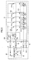
- Fig. 5 illustrates the circuit configuration of the printing controller 40 and the print head 13 shown in Fig. 4 .
- the printing controller 40 and print head 13 are electrically connected by means of cables 70.
- the cables 70 have connectors 71 connected to the printing controller 40 and connectors 72 connected to the print head 13, and can be any type of transmission line with a specific impedance including a coaxial cable and twisted pair.
- the shift register 110 shifts the received data from the first stage FF 111-1 to the last stage FF 111-n on the serial clock SCK, thereby outputting outputs from the output terminals Q1 to Qn.
- the printing controller 40 includes a circuit (not shown) that supplies the serial data SI and the serial clock SCK to the print head 13, a plurality of driver circuits 41 that drive the arrays 200 of light emitting elements in a time division manner, a power supply terminal, and a ground terminal. Only one of the driver circuits 41 is shown in Fig. 5 .
- the arrays 200 of light emitting elements include a total of 4992 light emitting thyristors.
- the 4992 light emitting thyristors are grouped into a plurality of groups, each group being driven by a corresponding driver circuit 41 simultaneously.
- A4 size paper or A3 size paper has a print circuit board having a length corresponding to the size of print medium.
- Signal paths formed on a print circuit board may also have specific characteristic impedances, and signal reflection may occur if the signal paths are formed without considering characteristic impedances thereof.
- the driver circuit 41 includes a drive source in the form of, for example a constant current circuit 42.
- the constant current circuit 42 has an NMOS transistor 43 that operates in its saturation region.
- the NMOS transistor 43 has a gate to which a bias voltage Vb is applied, a drain connected to the data terminal D, and operates in its saturation region to supply the drive current Iout to the data terminal D.
- the data terminal D is connected to the common terminal IN of the print head 13 through the connector 71, the cable 70, and the connector 72.
- Figs. 6A-6D illustrate light emitting thyristor 210 shown in Fig. 5 .
- the light emitting thyristor 210 includes an anode A, a cathode K, and a gate G.
- Fig. 6B is a cross-sectional view of the light emitting thyristor 210.
- the light emitting thyristor 210 is fabricated by, for example, epitaxially growing a predetermined crystal on a GaAs wafer by known metal organic chemical vapor deposition (MO-CVD).
- MO-CVD metal organic chemical vapor deposition
- a predetermined sacrificial layer and a buffer layer are epitaxially grown on a wafer substrate, and a three-layer structure is then fabricated.
- the three-layer structure includes an N-type layer 211 that contains an N-type impurity, a P-type layer 212 that contains a P-type impurity, and an N-type layer 213 that contains an N-type impurity, layered in this order.
- a P-type impurity region 214 is then selectively formed in the uppermost N-type layer 213 by photolithography. Grooves are formed in the wafer to define individual devices by a known etching technique.
- etching When etching is performed, a part of the N-type 211, which is the lowest layer of the light emitting thyristor 210, is exposed. Likewise, a part of the P-type layer 215, which is the uppermost layer, is exposed. A metal wiring is formed on the exposed region of the P-type layer 215 to form the anode A. At the same time, the gate G is formed on the N-type layer 212.
- the light emitting thyristor 210 is constituted of a PNP transistor 221 and an NPN transistor 222.
- the emitter of the PNP transistor 221 corresponds to the anode A of the light emitting thyristors 210 and the base of the PNP transistor 222 corresponds to the gate G.
- the gate electrode is also connected to the collector of the NPN transistor 222.
- the collector of the PNP transistor 221 is connected to the base of the NPN transistor 222.
- the emitter of the NPN transistor 222 corresponds to the cathode K of the light emitting thyristor 210.
- VDD the power supply voltage
- Vf the anode-cathode voltage of a light emitting thyristor being turned on (e.g., 210-1)
- R is the resistance of the resistor 47.
- the ON voltage (VoL) of the NMOS transistor 46 can be neglected for simplicity.
- the characteristic impedance of the cable 70 is a function of the dielectric constant of the dielectric material, the shape of cross section, and the ratio of the external diameter of the inner conductor to the internal diameter of the outer conductor, and has a specific value such as 50 ohms, 75 ohms, or 100 ohms depending on the material. Therefore, the characteristic impedance of the cable 70 cannot be set at will independently of the resistor 47.
- Fig. 8A is an equivalent circuit of the driver circuit 41A and the light emitting thyristor 200.
- Fig. 8B illustrates the current waveforms.
- the driver circuit 41A is constituted of a drive source 44A corresponding to the inverter 44 and an output resistor 47A corresponding to the current limiting resistor 47.
- Current Is flows through the output resistor 47A.
- the cable 70 has a characteristic impedance Zo, and a delay time Td.
- the light emitting thyristor 210 has a junction capacitance Cj across the anode and cathode. Current Id flows through the light emitting thyristor 210.
- Fig. 8A differs from Figs. 5 and 7 in that the anode is connected to the cable 70 and the cathode is connected to the ground GND. However, the circuit shown in Fig. 7 is equivalent to that shown in Fig. 5 as long as high frequency characteristics are concerned.
- Fig. 8B plots time t as the abscissa and current Is and current Id as the ordinate. Ton denotes the ON time of the driver circuit 44A. Toff denotes the OFF time of the driver circuit 44A.
- Tr denotes the rise time of the current Id and Tf denotes the fall time of the current Id.
- the current Id outputted from the cable 70 arrives at the light emitting thyristor after the delay time Td, and begins to rise.
- the light emitting thyristor 210 acts as a capacitor (junction capacitor Cj) which in turn causes reflection of signal so that a reflection wave travels toward the driver source 44A through the cable 70.
- the reflected wave is again reflected by the internal impedance of the driver source 44A, and travels back toward the light emitting array 200 again through the cable 70.
- Reflection of signal may also present a problem in achieving high speed operation of the light emitting thyristors. This problem will be described further.
- the current Id has ripples having a period of 2 ⁇ Td at its rising edge. Therefore, the current Id rises in rise time Tr due to multiple reflections that occur between the drive source 44A and the light emitting thyristor 210 through the cable 70. In other words, even though the current Is rises up sharply, the current Id does not sharply rise.
- the length L of the cable 70 is restricted by arrangement of components in the image forming apparatus 1.
- the four process units 101-1 to 10-4 for black (K), yellow (Y), magenta (M), and cyan (C) are aligned in order in a tandem electrophotographic color printer. Therefore, the cables 70 that connect the printing controller 40 and the print heads 13 of the four process units 101-1 to 10-4 have different lengths.
- the longest cable could be longer than 1 m.
- the rise time Tr and fall time Tf of the current Id increase, which is an obstacle to high speed operation of the print head 13A.
- Reflection of signal may be alleviated by improving the impedance matching between the characteristic impedance of the cable 70 and the output resistance 47A of the drive source 44A. However, they are determined by different factors and are difficult to be matched.
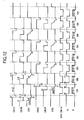
- Fig. 9 is a timing chart illustrating the details of the operation of the printing controller and print head.
- the serial data SI is set to the High level prior to the scanning of one line.
- the first pulse SCK1 of the serial clock pulse SCK is inputted.
- the serial data SI is input into the first FF 111-1 of the shift register 110 and the output terminal Q1 of the first FF 111-1 goes high (High level) after a short delay time.
- the serial data SI is again set to the L level at time t3, which is a predetermined time after the first pulse SCK1 has risen.
- the light output of each of the light emitting thyristors 210-1 to 210-8 is determined by the cathode current Ik that flows from anode to cathode.
- the use of the driver circuit 41 having the constant current circuit 42 maintains the drive current, e.g., Ik at a constant value even if the anode-cathode voltage when the light emitting thyristor turns on varies from thyristor to thyristor.
- the ON/OFF command signal DRVON-P is set to the Low level to turn off the light emitting thyristor 210-2, causing the switch circuit 230 to turn on to set the anode-cathode voltage of the light emitter thyristor 210-2 to substantially 0 V.
- a voltage sufficient to cause gate current to flow can be applied across the gate and cathode of the thyristors.
- a voltage insufficient to cause gate current to flow can be applied across the gate and cathode of the light emitting thyristors, no voltage can be applied across the gate and cathode, or reverse voltage may be applied across the gate and cathode.
- the light emitting thyristor 210-1 remains turned on during a drive time period T1 and the light emitting thyristor 210-2 remains turned on during a drive time period T2.
- the time periods T1 and T2 may be changed in length, so that dots may be produced by an equal amount of exposing energy even if the amount of light emitted from individual light emitting thyristors varies from thyristor to thyristor.
- the print head 13 eliminates multiple occurrences of signal reflection between the driver circuit 41 and the light emitting thyristors 200 connected through the cable 70, which eliminates the change in the waveform of the drive current that in turn causes the change in exposing energy -- hence uneven print density. This operation solves the problem of increased rise time and fall time of the drive current Iout, thereby achieving high speed switching of the light emitting thyristors.
- the print head 13 provides an image forming apparatus which is excellent in space efficiency and light output efficiency.
- the print head 13 is particularly applicable to the full-color image forming apparatus 1 which employs a multiple of print heads, the print head 13 may also be applicable to monochrome image forming apparatus and multi-color image forming apparatus.
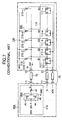
- a cable 70 has connectors 71 and 72, and electrically connects between a printing controller 40B and a print head 13B.
- the print head 13B includes a self-scanning shift register 110B which is of a different configuration from the shift register 110 of the first embodiment, arrays of light emitting elements similar to those of the first embodiment, and a switching means (e.g., bipolar NPN transistor) 233 different from the first embodiment.
- a switching means e.g., bipolar NPN transistor
- the print head 13B is constituted of a plurality of stages 120 formed of self-scanning thyristors, and supplies trigger current to the array 200 to turn on a corresponding light emitting thyristor.
- the self-scanning shift register 110B includes, for example, 4992 stages i.e., 200-1 to 200-4992. Each stage includes a self-scanning thyristor 121 having an anode connected to a VDD terminal, a diode 122 having a cathode connected to the gate of the self-scanning thyristor 121, and a resistor 123 connected across the gate of the self-scanning thyristor 121 and the ground GND.
- the self-scanning thyristor 121 of each of the odd-numbered stages 120-1, 120-3, 120-5, ... has an anode connected to the VDD terminal, a cathode connected to the connector 72 through a resistor 124-1, and a gate connected to the ground GND through the resistor 123.
- the gate of the self-scanning thyristor 121 of the first stage is connected to the cathode of the diode 122 whose anode is connected to the connector 72 through the connector 124-2.
- the gates of the self-scanning thyristors 121 of adjacent stages are connected via the diode 122.
- the self-scanning thyristor 121 of each of even-numbered stages 120-2, 120-4, 120-6, ... has an anode connected to the VDD terminal, a cathode connected to the connector 72 through the resistor 124-2, and a gate connected to the ground GND through the resistor 123.
- the gate of self-scanning thyristor 121 of each stage is connected to the output Q1, Q2, Q3, Q4, Q5, ... Qn of the self-scanning shift register 110B.
- the self-scanning thyristor 121 in each of stages 120-1, 120-2, 120-3, ... 120-n has a similar layer structure to the light emitting thyristors 210 of the array 200 of light emitting elements, and operates much the same way as the array 200 of light emitting elements.
- the self-scanning thyristor 121 does not have to emit light and is therefore covered with a metal film from above to block the light.
- the diode 122 connects between the gates of the self-scanning thyristors in adjacent stages, and determines the order (e.g., leftward in Fig. 10 ) in which the light emitting thyristors 210-1 to 210-n are turned on sequentially one at a time.
- the NPN transistor 233 operates to turn on the array 200 of light emitting elements in response to the ON/OFF command signal DRVON-N, where N implies negative logic.
- the NPN transistor 233 has a collector connected to the VDD terminal, an emitter connected to a common terminal IN.
- the whole circuit is fabricated on a GaAs wafer and therefore the MOS transistors of the switch circuit 230 of the first embodiment cannot be fabricated.
- the NPN transistor 233 is in a GaAs configuration.
- the printing controller 40B includes a circuit (not shown) that supplies the ON/OFF command signal DRVON-N to the print heads 13B, a plurality of driver circuits 41, a clock driver circuit 44, and power supply and ground terminals (not shown).
- the ON/OFF command signal DRVON-N commands the ON and OFF of the array of light emitting elements.
- the plurality of driver circuit 41 is similar to those of the first embodiment that drive a plurality of arrays of light emitting elements in a time division manner.
- the clock driver circuit 44 supplies a clock signal to the self-scanning shift register 110B.
- Fig. 10 shows only one driver circuit 41 for simplicity's sake.
- the groups are driven in a time division manner, so that any light emitting thyristors to be turned on in each group are driven before those in remaining group are driven.
- the clock driver circuit 44 has a plurality of output terminals CK1R, CK1C, CK2R, and CK2C which output clock signals.
- the output terminals CK1R, CK1C, CK2R, and CK2C are connected to a three-state buffer (not shown).
- Three-state buffers are a circuit having a CMOS output driver that allows no output state (i.e., a high-impedance state, hereinafter referred to Hi-Z state) in addition to the fundamental Low and High levels, effectively "removing" the output from the circuit.
- Figs. 11A-11C illustrate the structure of the NPN transistor 233 shown in Fig. 10 .
- the NPN transistor 233 is fabricated as follows: Referring to Fig. 11B , a buffer layer and a sacrificial layer (not shown) are epitaxially grown on a wafer. A three-layer structure is then formed on the wafer.
- the three-layer structure includes the N type layer 233a formed of AlGaAs doped with an N type impurity, the P type layer 233b doped with a P type impurity, and the N type layer 233c doped with an N type impurity. Grooves are formed in the three-layer structure by a known etching method to define individual devices.
- a power supply voltage VDD is applied to the anode of the light emitting thyristor 210.
- An NMOS transistor 43 is connected to the cathode of the light emitting thyristor 210 through the connector 72, cable 70, connector 71, and data terminal D.
- the transistor 43 is substantially in its conducting region, pulling down the voltage of the cathode so that a voltage of substantially equal to the power supply voltage VDD is applied across the anode and cathode of the light emitting thyristor 210.
- the gate of a light emitting thyristor 210 receives a High level signal, the Light emitting thyristor 210 is triggered to turn on.
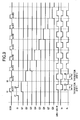
- Fig. 12 illustrates the waveform of signals when the light emitting thyristors 210-1 to 210-8 shown in Fig. 10 are sequentially turned on one at a time during the printing operation of the image forming apparatus shown in Fig. 1 .
- the self-scanning shift register 110B using the self-scanning thyristor 121 is clocked by a two-phase clock supplied from the clock terminals CK1 and CK2 of the clock driver circuit 44.
- the clock driver circuit 44 has the clock terminals CK1C and CK1R for clocks in one of two phases and the clock terminals CK2 and CK2R for clocks in the other of the two phases.
- the clock terminals CK1R, CK1C, CK2R, and CK2C are driven by a three-state buffer includes a CMOS output driver that allows no output state (Hi-Z state) in addition to the fundamental Low level and High level, effectively "removing" the output from the circuit.
- the thyristor 121 of the first stage 120-1 and the light emitting thyristor 210-1 have their gates connected together, and therefore trigger current flows through the gate of the thyristor 210-1 to turn on the light emitting thyristor 210-1.
- the light emitting thyristor 210-1 remains on until the ON/OFF command signal DRVON-N goes high (High level) to turn on the NPN transistor 233.
- the output terminal CK2R is set to the Low level. Current flows from the output terminal CK2C to the output terminal CK2R through the capacitor 4 6-2 and the resistor 45-2, charging the capacitor 46-2 to cause the voltage across the capacitor 46-2 to increase. Accordingly, the potential at the clock terminal CK2 decreases toward the ground GND as depicted at "c".
- the thyristor 121 of the second stage 120-2 and the light emitting thyristor 210-2 have their gates connected together, and therefore trigger current flows through the gate of the light emitting thyristor 210-2 to turn on the light emitting thyristor 210-2.
- the light emitting thyristor 210-2 remains on until the ON/OFF command signal DRVON-N goes high (High level) to turn on the NPN transistor 233.
- the output terminal CK1R is set to the Low level. Current flows from the output terminal CK1C to the output terminal CK1R through the capacitor 46-1 and the resistor 45-1, charging the capacitor 46-1 to cause the voltage across the capacitor 46-1 to increase. Accordingly, the potential at the clock terminal CK1 decreases toward the ground GND as depicted at "e".
- the output terminal CK1C is set to the Low level, so that the output terminal CK1R enters the Hi-Z state as depicted by a dotted line and is at a mid potential between the High level and the Low level. Since the output terminal CK1R enters the Hi-Z state at time t17, a waveform having undershoot waveform appears on the clock terminal CK1 as depicted at "f" in Fig. 12 . This undershoot waveform is caused by a voltage that charges the capacitor 46-1.
- the three-state output buffer (not shown) in the clock driver circuit 44 shown in Fig. 10 has a parasitic diode.
- the undershoot waveform causes current to flow through the parasitic diode so that the negative voltage at "f" is clamped. This maintains the negative peak of the undershoot waveform at "f” at about -0.6 V.
- the capacitor 46-1 discharges gradually so that the voltage across the capacitor 46-1 gradually decreases. Thus, the undershoot waveform depicted at "f" will decay with time.
- the gate of the thyristors 121 which remain turned on are at about the High level, and the gate of the thyristors 121 which remain turned off are at about the Low level, nearly ground level GND.
- the gate potential of the thyristor 121 is supplied from the output terminals Q1-Q8 of the shift register 110B.
- the light emitting thyristors 210-1 to 210-8 can be turned on in sequence one at a time in accordance with the command signals from the shift register 110B.
- the currents Io and Ik have waveforms complementary to each other such that when the current Io flows, the current Ik is about zero and vice versa.
- the sum of the currents Io and Ik is equal to the current Iout.
- the comparative example shown in Fig. 7 presents a problem in that current flows intermittently through the cable 70 as the light emitting thyristors 210-1 to 210-8 turn on and off, causing multiple reflections of signal to occur between the driver circuit 44A and the print head 13A, and hence distortion of the current waveforms and prolonged transition time of the light emitting thyristors.
- the present invention is not limited to the above-described first and second embodiments but may be modified in a variety of ways, including the following modifications.
Landscapes
- Physics & Mathematics (AREA)
- Optics & Photonics (AREA)
- Health & Medical Sciences (AREA)
- General Health & Medical Sciences (AREA)
- Toxicology (AREA)
- Printers Or Recording Devices Using Electromagnetic And Radiation Means (AREA)
- Facsimile Heads (AREA)
Applications Claiming Priority (1)
| Application Number | Priority Date | Filing Date | Title |
|---|---|---|---|
| JP2010011594A JP5460350B2 (ja) | 2010-01-22 | 2010-01-22 | 駆動回路、駆動装置及び画像形成装置 |
Publications (2)
| Publication Number | Publication Date |
|---|---|
| EP2347909A1 EP2347909A1 (en) | 2011-07-27 |
| EP2347909B1 true EP2347909B1 (en) | 2014-05-07 |
Family
ID=43836597
Family Applications (1)
| Application Number | Title | Priority Date | Filing Date |
|---|---|---|---|
| EP11151263.8A Not-in-force EP2347909B1 (en) | 2010-01-22 | 2011-01-18 | Driver circuit, driver apparatus, and image forming apparatus |
Country Status (4)
| Country | Link |
|---|---|
| US (1) | US8742824B2 (enExample) |
| EP (1) | EP2347909B1 (enExample) |
| JP (1) | JP5460350B2 (enExample) |
| CN (1) | CN102166888B (enExample) |
Cited By (1)
| Publication number | Priority date | Publication date | Assignee | Title |
|---|---|---|---|---|
| TWI634017B (zh) * | 2017-12-14 | 2018-09-01 | 虹光精密工業股份有限公司 | 具有識別紙匣模組功能之紙匣裝置 |
Families Citing this family (2)
| Publication number | Priority date | Publication date | Assignee | Title |
|---|---|---|---|---|
| JP5366511B2 (ja) * | 2008-11-14 | 2013-12-11 | 株式会社沖データ | 駆動回路、光プリントヘッド及び画像形成装置 |
| JP7192642B2 (ja) * | 2019-04-24 | 2022-12-20 | 沖電気工業株式会社 | 半導体複合装置、プリントヘッド及び画像形成装置 |
Family Cites Families (9)
| Publication number | Priority date | Publication date | Assignee | Title |
|---|---|---|---|---|
| JPH0817201A (ja) * | 1994-06-27 | 1996-01-19 | Matsushita Electric Works Ltd | 携帯用照明装置 |
| JPH09199760A (ja) * | 1996-01-22 | 1997-07-31 | Canon Inc | 光量制御装置及び光量制御方法 |
| JP3308801B2 (ja) * | 1996-03-06 | 2002-07-29 | キヤノン株式会社 | 記録素子アレイ |
| JP4438174B2 (ja) | 2000-04-06 | 2010-03-24 | 富士ゼロックス株式会社 | 自己走査型発光素子アレイの駆動方法 |
| US6703790B2 (en) * | 2000-04-06 | 2004-03-09 | Nippon Sheet Glass Co., Ltd. | Method for driving a self-scanning light-emitting array |
| JP4817774B2 (ja) * | 2005-09-14 | 2011-11-16 | 株式会社沖データ | 半導体複合装置光プリントヘッドおよび画像形成装置 |
| JP4545203B2 (ja) * | 2008-03-18 | 2010-09-15 | 株式会社沖データ | 光プリントヘッドおよび画像形成装置 |
| JP2009289836A (ja) * | 2008-05-27 | 2009-12-10 | Oki Data Corp | 発光素子アレイ、駆動制御装置、記録ヘッドおよび画像形成装置 |
| JP2010045230A (ja) * | 2008-08-13 | 2010-02-25 | Fuji Xerox Co Ltd | 発光素子チップ、露光装置および画像形成装置 |
-
2010
- 2010-01-22 JP JP2010011594A patent/JP5460350B2/ja not_active Expired - Fee Related
-
2011
- 2011-01-18 EP EP11151263.8A patent/EP2347909B1/en not_active Not-in-force
- 2011-01-20 US US12/929,383 patent/US8742824B2/en not_active Expired - Fee Related
- 2011-01-21 CN CN201110023924.XA patent/CN102166888B/zh not_active Expired - Fee Related
Cited By (2)
| Publication number | Priority date | Publication date | Assignee | Title |
|---|---|---|---|---|
| TWI634017B (zh) * | 2017-12-14 | 2018-09-01 | 虹光精密工業股份有限公司 | 具有識別紙匣模組功能之紙匣裝置 |
| US10732910B2 (en) | 2017-12-14 | 2020-08-04 | Avision Inc. | Tray device capable of recognizing tray modules |
Also Published As
| Publication number | Publication date |
|---|---|
| CN102166888B (zh) | 2015-02-25 |
| JP5460350B2 (ja) | 2014-04-02 |
| EP2347909A1 (en) | 2011-07-27 |
| US20110181640A1 (en) | 2011-07-28 |
| US8742824B2 (en) | 2014-06-03 |
| JP2011148196A (ja) | 2011-08-04 |
| CN102166888A (zh) | 2011-08-31 |
Similar Documents
| Publication | Publication Date | Title |
|---|---|---|
| US8258723B2 (en) | Light-emitting element array, driving device, and image forming apparatus | |
| US8848012B2 (en) | Drive device, print head and image forming apparatus | |
| EP2511770B1 (en) | Driver apparatus, print head and image forming apparatus | |
| US7924304B2 (en) | Light-emitting element array, drive controlling device, recording head, and image forming device | |
| US8542262B2 (en) | Light emitting element array, drive circuit, optical print head, and image forming apparatus | |
| US8581946B2 (en) | Driving device, optical print head and image forming device | |
| EP2347909B1 (en) | Driver circuit, driver apparatus, and image forming apparatus | |
| US8835974B2 (en) | Driving device, print head and image forming device | |
| JP2011243910A (ja) | 駆動装置、プリントヘッド及び画像形成装置 | |
| US9048841B2 (en) | Driver circuit, driver apparatus, and image forming apparatus | |
| US8836743B2 (en) | Drive device, print head and image forming apparatus | |
| US20110262184A1 (en) | Driver circuit, print head, and image forming apparatus | |
| US8587628B2 (en) | Driver apparatus, print head, and image forming apparatus | |
| JP5676342B2 (ja) | 駆動装置、プリントヘッド及び画像形成装置 | |
| JP2012045888A (ja) | 駆動装置、プリントヘッド及び画像形成装置 | |
| JP2012051125A (ja) | 駆動装置、プリントヘッド及び画像形成装置 |
Legal Events
| Date | Code | Title | Description |
|---|---|---|---|
| PUAI | Public reference made under article 153(3) epc to a published international application that has entered the european phase |
Free format text: ORIGINAL CODE: 0009012 |
|
| AK | Designated contracting states |
Kind code of ref document: A1 Designated state(s): AL AT BE BG CH CY CZ DE DK EE ES FI FR GB GR HR HU IE IS IT LI LT LU LV MC MK MT NL NO PL PT RO RS SE SI SK SM TR |
|
| AX | Request for extension of the european patent |
Extension state: BA ME |
|
| 17P | Request for examination filed |
Effective date: 20120118 |
|
| GRAP | Despatch of communication of intention to grant a patent |
Free format text: ORIGINAL CODE: EPIDOSNIGR1 |
|
| INTG | Intention to grant announced |
Effective date: 20131125 |
|
| GRAS | Grant fee paid |
Free format text: ORIGINAL CODE: EPIDOSNIGR3 |
|
| GRAA | (expected) grant |
Free format text: ORIGINAL CODE: 0009210 |
|
| AK | Designated contracting states |
Kind code of ref document: B1 Designated state(s): AL AT BE BG CH CY CZ DE DK EE ES FI FR GB GR HR HU IE IS IT LI LT LU LV MC MK MT NL NO PL PT RO RS SE SI SK SM TR |
|
| REG | Reference to a national code |
Ref country code: GB Ref legal event code: FG4D |
|
| REG | Reference to a national code |
Ref country code: AT Ref legal event code: REF Ref document number: 666312 Country of ref document: AT Kind code of ref document: T Effective date: 20140515 |
|
| REG | Reference to a national code |
Ref country code: IE Ref legal event code: FG4D |
|
| REG | Reference to a national code |
Ref country code: DE Ref legal event code: R096 Ref document number: 602011006654 Country of ref document: DE Effective date: 20140618 |
|
| REG | Reference to a national code |
Ref country code: NL Ref legal event code: T3 |
|
| REG | Reference to a national code |
Ref country code: AT Ref legal event code: MK05 Ref document number: 666312 Country of ref document: AT Kind code of ref document: T Effective date: 20140507 |
|
| REG | Reference to a national code |
Ref country code: LT Ref legal event code: MG4D |
|
| PG25 | Lapsed in a contracting state [announced via postgrant information from national office to epo] |
Ref country code: CY Free format text: LAPSE BECAUSE OF FAILURE TO SUBMIT A TRANSLATION OF THE DESCRIPTION OR TO PAY THE FEE WITHIN THE PRESCRIBED TIME-LIMIT Effective date: 20140507 Ref country code: GR Free format text: LAPSE BECAUSE OF FAILURE TO SUBMIT A TRANSLATION OF THE DESCRIPTION OR TO PAY THE FEE WITHIN THE PRESCRIBED TIME-LIMIT Effective date: 20140808 Ref country code: IS Free format text: LAPSE BECAUSE OF FAILURE TO SUBMIT A TRANSLATION OF THE DESCRIPTION OR TO PAY THE FEE WITHIN THE PRESCRIBED TIME-LIMIT Effective date: 20140907 Ref country code: LT Free format text: LAPSE BECAUSE OF FAILURE TO SUBMIT A TRANSLATION OF THE DESCRIPTION OR TO PAY THE FEE WITHIN THE PRESCRIBED TIME-LIMIT Effective date: 20140507 Ref country code: FI Free format text: LAPSE BECAUSE OF FAILURE TO SUBMIT A TRANSLATION OF THE DESCRIPTION OR TO PAY THE FEE WITHIN THE PRESCRIBED TIME-LIMIT Effective date: 20140507 Ref country code: NO Free format text: LAPSE BECAUSE OF FAILURE TO SUBMIT A TRANSLATION OF THE DESCRIPTION OR TO PAY THE FEE WITHIN THE PRESCRIBED TIME-LIMIT Effective date: 20140807 |
|
| PG25 | Lapsed in a contracting state [announced via postgrant information from national office to epo] |
Ref country code: AT Free format text: LAPSE BECAUSE OF FAILURE TO SUBMIT A TRANSLATION OF THE DESCRIPTION OR TO PAY THE FEE WITHIN THE PRESCRIBED TIME-LIMIT Effective date: 20140507 Ref country code: ES Free format text: LAPSE BECAUSE OF FAILURE TO SUBMIT A TRANSLATION OF THE DESCRIPTION OR TO PAY THE FEE WITHIN THE PRESCRIBED TIME-LIMIT Effective date: 20140507 Ref country code: SE Free format text: LAPSE BECAUSE OF FAILURE TO SUBMIT A TRANSLATION OF THE DESCRIPTION OR TO PAY THE FEE WITHIN THE PRESCRIBED TIME-LIMIT Effective date: 20140507 Ref country code: HR Free format text: LAPSE BECAUSE OF FAILURE TO SUBMIT A TRANSLATION OF THE DESCRIPTION OR TO PAY THE FEE WITHIN THE PRESCRIBED TIME-LIMIT Effective date: 20140507 Ref country code: RS Free format text: LAPSE BECAUSE OF FAILURE TO SUBMIT A TRANSLATION OF THE DESCRIPTION OR TO PAY THE FEE WITHIN THE PRESCRIBED TIME-LIMIT Effective date: 20140507 Ref country code: PL Free format text: LAPSE BECAUSE OF FAILURE TO SUBMIT A TRANSLATION OF THE DESCRIPTION OR TO PAY THE FEE WITHIN THE PRESCRIBED TIME-LIMIT Effective date: 20140507 Ref country code: LV Free format text: LAPSE BECAUSE OF FAILURE TO SUBMIT A TRANSLATION OF THE DESCRIPTION OR TO PAY THE FEE WITHIN THE PRESCRIBED TIME-LIMIT Effective date: 20140507 |
|
| PG25 | Lapsed in a contracting state [announced via postgrant information from national office to epo] |
Ref country code: PT Free format text: LAPSE BECAUSE OF FAILURE TO SUBMIT A TRANSLATION OF THE DESCRIPTION OR TO PAY THE FEE WITHIN THE PRESCRIBED TIME-LIMIT Effective date: 20140908 |
|
| PG25 | Lapsed in a contracting state [announced via postgrant information from national office to epo] |
Ref country code: DK Free format text: LAPSE BECAUSE OF FAILURE TO SUBMIT A TRANSLATION OF THE DESCRIPTION OR TO PAY THE FEE WITHIN THE PRESCRIBED TIME-LIMIT Effective date: 20140507 Ref country code: EE Free format text: LAPSE BECAUSE OF FAILURE TO SUBMIT A TRANSLATION OF THE DESCRIPTION OR TO PAY THE FEE WITHIN THE PRESCRIBED TIME-LIMIT Effective date: 20140507 Ref country code: SK Free format text: LAPSE BECAUSE OF FAILURE TO SUBMIT A TRANSLATION OF THE DESCRIPTION OR TO PAY THE FEE WITHIN THE PRESCRIBED TIME-LIMIT Effective date: 20140507 Ref country code: RO Free format text: LAPSE BECAUSE OF FAILURE TO SUBMIT A TRANSLATION OF THE DESCRIPTION OR TO PAY THE FEE WITHIN THE PRESCRIBED TIME-LIMIT Effective date: 20140507 Ref country code: CZ Free format text: LAPSE BECAUSE OF FAILURE TO SUBMIT A TRANSLATION OF THE DESCRIPTION OR TO PAY THE FEE WITHIN THE PRESCRIBED TIME-LIMIT Effective date: 20140507 Ref country code: BE Free format text: LAPSE BECAUSE OF FAILURE TO SUBMIT A TRANSLATION OF THE DESCRIPTION OR TO PAY THE FEE WITHIN THE PRESCRIBED TIME-LIMIT Effective date: 20140507 |
|
| REG | Reference to a national code |
Ref country code: DE Ref legal event code: R097 Ref document number: 602011006654 Country of ref document: DE |
|
| PLBE | No opposition filed within time limit |
Free format text: ORIGINAL CODE: 0009261 |
|
| STAA | Information on the status of an ep patent application or granted ep patent |
Free format text: STATUS: NO OPPOSITION FILED WITHIN TIME LIMIT |
|
| 26N | No opposition filed |
Effective date: 20150210 |
|
| PG25 | Lapsed in a contracting state [announced via postgrant information from national office to epo] |
Ref country code: IT Free format text: LAPSE BECAUSE OF FAILURE TO SUBMIT A TRANSLATION OF THE DESCRIPTION OR TO PAY THE FEE WITHIN THE PRESCRIBED TIME-LIMIT Effective date: 20140507 |
|
| REG | Reference to a national code |
Ref country code: DE Ref legal event code: R097 Ref document number: 602011006654 Country of ref document: DE Effective date: 20150210 |
|
| PG25 | Lapsed in a contracting state [announced via postgrant information from national office to epo] |
Ref country code: SI Free format text: LAPSE BECAUSE OF FAILURE TO SUBMIT A TRANSLATION OF THE DESCRIPTION OR TO PAY THE FEE WITHIN THE PRESCRIBED TIME-LIMIT Effective date: 20140507 |
|
| REG | Reference to a national code |
Ref country code: CH Ref legal event code: PL |
|
| PG25 | Lapsed in a contracting state [announced via postgrant information from national office to epo] |
Ref country code: LU Free format text: LAPSE BECAUSE OF FAILURE TO SUBMIT A TRANSLATION OF THE DESCRIPTION OR TO PAY THE FEE WITHIN THE PRESCRIBED TIME-LIMIT Effective date: 20150118 |
|
| PG25 | Lapsed in a contracting state [announced via postgrant information from national office to epo] |
Ref country code: MC Free format text: LAPSE BECAUSE OF FAILURE TO SUBMIT A TRANSLATION OF THE DESCRIPTION OR TO PAY THE FEE WITHIN THE PRESCRIBED TIME-LIMIT Effective date: 20140507 |
|
| PG25 | Lapsed in a contracting state [announced via postgrant information from national office to epo] |
Ref country code: CH Free format text: LAPSE BECAUSE OF NON-PAYMENT OF DUE FEES Effective date: 20150131 Ref country code: LI Free format text: LAPSE BECAUSE OF NON-PAYMENT OF DUE FEES Effective date: 20150131 |
|
| REG | Reference to a national code |
Ref country code: IE Ref legal event code: MM4A |
|
| REG | Reference to a national code |
Ref country code: FR Ref legal event code: PLFP Year of fee payment: 6 |
|
| PG25 | Lapsed in a contracting state [announced via postgrant information from national office to epo] |
Ref country code: IE Free format text: LAPSE BECAUSE OF NON-PAYMENT OF DUE FEES Effective date: 20150118 |
|
| REG | Reference to a national code |
Ref country code: FR Ref legal event code: PLFP Year of fee payment: 7 |
|
| PG25 | Lapsed in a contracting state [announced via postgrant information from national office to epo] |
Ref country code: MT Free format text: LAPSE BECAUSE OF FAILURE TO SUBMIT A TRANSLATION OF THE DESCRIPTION OR TO PAY THE FEE WITHIN THE PRESCRIBED TIME-LIMIT Effective date: 20140507 |
|
| PG25 | Lapsed in a contracting state [announced via postgrant information from national office to epo] |
Ref country code: HU Free format text: LAPSE BECAUSE OF FAILURE TO SUBMIT A TRANSLATION OF THE DESCRIPTION OR TO PAY THE FEE WITHIN THE PRESCRIBED TIME-LIMIT; INVALID AB INITIO Effective date: 20110118 Ref country code: SM Free format text: LAPSE BECAUSE OF FAILURE TO SUBMIT A TRANSLATION OF THE DESCRIPTION OR TO PAY THE FEE WITHIN THE PRESCRIBED TIME-LIMIT Effective date: 20140507 Ref country code: BG Free format text: LAPSE BECAUSE OF FAILURE TO SUBMIT A TRANSLATION OF THE DESCRIPTION OR TO PAY THE FEE WITHIN THE PRESCRIBED TIME-LIMIT Effective date: 20140507 |
|
| PG25 | Lapsed in a contracting state [announced via postgrant information from national office to epo] |
Ref country code: TR Free format text: LAPSE BECAUSE OF FAILURE TO SUBMIT A TRANSLATION OF THE DESCRIPTION OR TO PAY THE FEE WITHIN THE PRESCRIBED TIME-LIMIT Effective date: 20140507 |
|
| REG | Reference to a national code |
Ref country code: FR Ref legal event code: PLFP Year of fee payment: 8 |
|
| PG25 | Lapsed in a contracting state [announced via postgrant information from national office to epo] |
Ref country code: MK Free format text: LAPSE BECAUSE OF FAILURE TO SUBMIT A TRANSLATION OF THE DESCRIPTION OR TO PAY THE FEE WITHIN THE PRESCRIBED TIME-LIMIT Effective date: 20140507 |
|
| PG25 | Lapsed in a contracting state [announced via postgrant information from national office to epo] |
Ref country code: AL Free format text: LAPSE BECAUSE OF FAILURE TO SUBMIT A TRANSLATION OF THE DESCRIPTION OR TO PAY THE FEE WITHIN THE PRESCRIBED TIME-LIMIT Effective date: 20140507 |
|
| PGFP | Annual fee paid to national office [announced via postgrant information from national office to epo] |
Ref country code: NL Payment date: 20191212 Year of fee payment: 10 |
|
| PGFP | Annual fee paid to national office [announced via postgrant information from national office to epo] |
Ref country code: FR Payment date: 20191216 Year of fee payment: 10 |
|
| PGFP | Annual fee paid to national office [announced via postgrant information from national office to epo] |
Ref country code: GB Payment date: 20200113 Year of fee payment: 10 Ref country code: DE Payment date: 20200107 Year of fee payment: 10 |
|
| REG | Reference to a national code |
Ref country code: DE Ref legal event code: R119 Ref document number: 602011006654 Country of ref document: DE |
|
| REG | Reference to a national code |
Ref country code: NL Ref legal event code: MM Effective date: 20210201 |
|
| GBPC | Gb: european patent ceased through non-payment of renewal fee |
Effective date: 20210118 |
|
| PG25 | Lapsed in a contracting state [announced via postgrant information from national office to epo] |
Ref country code: NL Free format text: LAPSE BECAUSE OF NON-PAYMENT OF DUE FEES Effective date: 20210201 Ref country code: FR Free format text: LAPSE BECAUSE OF NON-PAYMENT OF DUE FEES Effective date: 20210131 |
|
| PG25 | Lapsed in a contracting state [announced via postgrant information from national office to epo] |
Ref country code: GB Free format text: LAPSE BECAUSE OF NON-PAYMENT OF DUE FEES Effective date: 20210118 Ref country code: DE Free format text: LAPSE BECAUSE OF NON-PAYMENT OF DUE FEES Effective date: 20210803 |