EP2347455B1 - Strahlungsemittierendes bauelement und verfahren zu dessen herstellung - Google Patents
Strahlungsemittierendes bauelement und verfahren zu dessen herstellung Download PDFInfo
- Publication number
- EP2347455B1 EP2347455B1 EP09771686A EP09771686A EP2347455B1 EP 2347455 B1 EP2347455 B1 EP 2347455B1 EP 09771686 A EP09771686 A EP 09771686A EP 09771686 A EP09771686 A EP 09771686A EP 2347455 B1 EP2347455 B1 EP 2347455B1
- Authority
- EP
- European Patent Office
- Prior art keywords
- radiation
- layer
- contact
- semiconductor chip
- passivation layer
- Prior art date
- Legal status (The legal status is an assumption and is not a legal conclusion. Google has not performed a legal analysis and makes no representation as to the accuracy of the status listed.)
- Active
Links
- 238000004519 manufacturing process Methods 0.000 title description 3
- 239000004065 semiconductor Substances 0.000 claims description 112
- 238000002161 passivation Methods 0.000 claims description 93
- 230000005855 radiation Effects 0.000 claims description 62
- 230000003287 optical effect Effects 0.000 claims description 27
- 238000000034 method Methods 0.000 claims description 26
- 229920000620 organic polymer Polymers 0.000 claims description 19
- 238000006243 chemical reaction Methods 0.000 claims description 13
- 230000008569 process Effects 0.000 claims description 9
- 239000010409 thin film Substances 0.000 claims description 7
- 229910052801 chlorine Inorganic materials 0.000 claims description 6
- 239000000463 material Substances 0.000 claims description 6
- 230000005670 electromagnetic radiation Effects 0.000 claims description 4
- 239000010410 layer Substances 0.000 description 188
- 230000007613 environmental effect Effects 0.000 description 10
- 239000000126 substance Substances 0.000 description 10
- 239000000758 substrate Substances 0.000 description 10
- 230000004888 barrier function Effects 0.000 description 9
- 239000007789 gas Substances 0.000 description 8
- 238000001020 plasma etching Methods 0.000 description 6
- -1 alkalis Substances 0.000 description 5
- 230000000694 effects Effects 0.000 description 5
- XLYOFNOQVPJJNP-UHFFFAOYSA-N water Chemical compound O XLYOFNOQVPJJNP-UHFFFAOYSA-N 0.000 description 5
- XLOMVQKBTHCTTD-UHFFFAOYSA-N Zinc monoxide Chemical compound [Zn]=O XLOMVQKBTHCTTD-UHFFFAOYSA-N 0.000 description 4
- 239000002253 acid Substances 0.000 description 4
- 150000007513 acids Chemical class 0.000 description 4
- 239000002585 base Substances 0.000 description 4
- 238000005229 chemical vapour deposition Methods 0.000 description 4
- 229920000642 polymer Polymers 0.000 description 4
- 238000001228 spectrum Methods 0.000 description 4
- 239000000919 ceramic Substances 0.000 description 3
- 239000000460 chlorine Substances 0.000 description 3
- 125000001309 chloro group Chemical group Cl* 0.000 description 3
- 238000005538 encapsulation Methods 0.000 description 3
- 230000005693 optoelectronics Effects 0.000 description 3
- 238000000623 plasma-assisted chemical vapour deposition Methods 0.000 description 3
- 229920000265 Polyparaphenylene Polymers 0.000 description 2
- 238000010521 absorption reaction Methods 0.000 description 2
- 125000003118 aryl group Chemical group 0.000 description 2
- 230000008901 benefit Effects 0.000 description 2
- 230000005540 biological transmission Effects 0.000 description 2
- PMHQVHHXPFUNSP-UHFFFAOYSA-M copper(1+);methylsulfanylmethane;bromide Chemical compound Br[Cu].CSC PMHQVHHXPFUNSP-UHFFFAOYSA-M 0.000 description 2
- 239000000539 dimer Substances 0.000 description 2
- 229910052738 indium Inorganic materials 0.000 description 2
- 150000004767 nitrides Chemical class 0.000 description 2
- OJMIONKXNSYLSR-UHFFFAOYSA-N phosphorous acid Chemical compound OP(O)O OJMIONKXNSYLSR-UHFFFAOYSA-N 0.000 description 2
- 238000006116 polymerization reaction Methods 0.000 description 2
- 239000011787 zinc oxide Substances 0.000 description 2
- 0 CC(**)C(*)(*IC)c1c(*)c(C=*)c(C(*)(*)C(*)(*)c2c(*)c(I)c(C(*)(*)C(C)(*)*)c(C)c2*)c(C)c1* Chemical compound CC(**)C(*)(*IC)c1c(*)c(C=*)c(C(*)(*)C(*)(*)c2c(*)c(I)c(C(*)(*)C(C)(*)*)c(C)c2*)c(C)c1* 0.000 description 1
- XUIMIQQOPSSXEZ-UHFFFAOYSA-N Silicon Chemical compound [Si] XUIMIQQOPSSXEZ-UHFFFAOYSA-N 0.000 description 1
- 238000005299 abrasion Methods 0.000 description 1
- 238000004026 adhesive bonding Methods 0.000 description 1
- 238000000429 assembly Methods 0.000 description 1
- 230000000712 assembly Effects 0.000 description 1
- 230000015572 biosynthetic process Effects 0.000 description 1
- 230000008859 change Effects 0.000 description 1
- 150000001875 compounds Chemical class 0.000 description 1
- 238000009833 condensation Methods 0.000 description 1
- 230000005494 condensation Effects 0.000 description 1
- 238000010276 construction Methods 0.000 description 1
- 238000000151 deposition Methods 0.000 description 1
- 230000008021 deposition Effects 0.000 description 1
- 238000009826 distribution Methods 0.000 description 1
- 230000005684 electric field Effects 0.000 description 1
- 230000002209 hydrophobic effect Effects 0.000 description 1
- AMGQUBHHOARCQH-UHFFFAOYSA-N indium;oxotin Chemical compound [In].[Sn]=O AMGQUBHHOARCQH-UHFFFAOYSA-N 0.000 description 1
- 239000002346 layers by function Substances 0.000 description 1
- 229910052751 metal Inorganic materials 0.000 description 1
- 239000002184 metal Substances 0.000 description 1
- 229910001092 metal group alloy Inorganic materials 0.000 description 1
- 238000002156 mixing Methods 0.000 description 1
- 239000000203 mixture Substances 0.000 description 1
- 230000004048 modification Effects 0.000 description 1
- 238000012986 modification Methods 0.000 description 1
- 239000000178 monomer Substances 0.000 description 1
- 239000002114 nanocomposite Substances 0.000 description 1
- 239000000615 nonconductor Substances 0.000 description 1
- 238000012856 packing Methods 0.000 description 1
- 239000004038 photonic crystal Substances 0.000 description 1
- 230000000704 physical effect Effects 0.000 description 1
- 230000001681 protective effect Effects 0.000 description 1
- 229910052710 silicon Inorganic materials 0.000 description 1
- 239000010703 silicon Substances 0.000 description 1
- 238000005476 soldering Methods 0.000 description 1
- 238000003892 spreading Methods 0.000 description 1
- 230000007480 spreading Effects 0.000 description 1
- 238000007740 vapor deposition Methods 0.000 description 1
- YVTHLONGBIQYBO-UHFFFAOYSA-N zinc indium(3+) oxygen(2-) Chemical compound [O--].[Zn++].[In+3] YVTHLONGBIQYBO-UHFFFAOYSA-N 0.000 description 1
Images


Classifications
-
- C—CHEMISTRY; METALLURGY
- C08—ORGANIC MACROMOLECULAR COMPOUNDS; THEIR PREPARATION OR CHEMICAL WORKING-UP; COMPOSITIONS BASED THEREON
- C08G—MACROMOLECULAR COMPOUNDS OBTAINED OTHERWISE THAN BY REACTIONS ONLY INVOLVING UNSATURATED CARBON-TO-CARBON BONDS
- C08G61/00—Macromolecular compounds obtained by reactions forming a carbon-to-carbon link in the main chain of the macromolecule
- C08G61/02—Macromolecular compounds containing only carbon atoms in the main chain of the macromolecule, e.g. polyxylylenes
-
- H—ELECTRICITY
- H01—ELECTRIC ELEMENTS
- H01L—SEMICONDUCTOR DEVICES NOT COVERED BY CLASS H10
- H01L24/00—Arrangements for connecting or disconnecting semiconductor or solid-state bodies; Methods or apparatus related thereto
- H01L24/01—Means for bonding being attached to, or being formed on, the surface to be connected, e.g. chip-to-package, die-attach, "first-level" interconnects; Manufacturing methods related thereto
- H01L24/18—High density interconnect [HDI] connectors; Manufacturing methods related thereto
- H01L24/23—Structure, shape, material or disposition of the high density interconnect connectors after the connecting process
- H01L24/24—Structure, shape, material or disposition of the high density interconnect connectors after the connecting process of an individual high density interconnect connector
-
- H—ELECTRICITY
- H01—ELECTRIC ELEMENTS
- H01L—SEMICONDUCTOR DEVICES NOT COVERED BY CLASS H10
- H01L24/00—Arrangements for connecting or disconnecting semiconductor or solid-state bodies; Methods or apparatus related thereto
- H01L24/80—Methods for connecting semiconductor or other solid state bodies using means for bonding being attached to, or being formed on, the surface to be connected
- H01L24/82—Methods for connecting semiconductor or other solid state bodies using means for bonding being attached to, or being formed on, the surface to be connected by forming build-up interconnects at chip-level, e.g. for high density interconnects [HDI]
-
- H—ELECTRICITY
- H10—SEMICONDUCTOR DEVICES; ELECTRIC SOLID-STATE DEVICES NOT OTHERWISE PROVIDED FOR
- H10H—INORGANIC LIGHT-EMITTING SEMICONDUCTOR DEVICES HAVING POTENTIAL BARRIERS
- H10H20/00—Individual inorganic light-emitting semiconductor devices having potential barriers, e.g. light-emitting diodes [LED]
- H10H20/80—Constructional details
- H10H20/84—Coatings, e.g. passivation layers or antireflective coatings
-
- H—ELECTRICITY
- H10—SEMICONDUCTOR DEVICES; ELECTRIC SOLID-STATE DEVICES NOT OTHERWISE PROVIDED FOR
- H10H—INORGANIC LIGHT-EMITTING SEMICONDUCTOR DEVICES HAVING POTENTIAL BARRIERS
- H10H20/00—Individual inorganic light-emitting semiconductor devices having potential barriers, e.g. light-emitting diodes [LED]
- H10H20/80—Constructional details
- H10H20/85—Packages
- H10H20/857—Interconnections, e.g. lead-frames, bond wires or solder balls
-
- H—ELECTRICITY
- H01—ELECTRIC ELEMENTS
- H01L—SEMICONDUCTOR DEVICES NOT COVERED BY CLASS H10
- H01L2224/00—Indexing scheme for arrangements for connecting or disconnecting semiconductor or solid-state bodies and methods related thereto as covered by H01L24/00
- H01L2224/01—Means for bonding being attached to, or being formed on, the surface to be connected, e.g. chip-to-package, die-attach, "first-level" interconnects; Manufacturing methods related thereto
- H01L2224/18—High density interconnect [HDI] connectors; Manufacturing methods related thereto
- H01L2224/23—Structure, shape, material or disposition of the high density interconnect connectors after the connecting process
- H01L2224/24—Structure, shape, material or disposition of the high density interconnect connectors after the connecting process of an individual high density interconnect connector
- H01L2224/2405—Shape
- H01L2224/24051—Conformal with the semiconductor or solid-state device
-
- H—ELECTRICITY
- H01—ELECTRIC ELEMENTS
- H01L—SEMICONDUCTOR DEVICES NOT COVERED BY CLASS H10
- H01L2924/00—Indexing scheme for arrangements or methods for connecting or disconnecting semiconductor or solid-state bodies as covered by H01L24/00
- H01L2924/013—Alloys
- H01L2924/0132—Binary Alloys
- H01L2924/01327—Intermediate phases, i.e. intermetallics compounds
-
- H—ELECTRICITY
- H01—ELECTRIC ELEMENTS
- H01L—SEMICONDUCTOR DEVICES NOT COVERED BY CLASS H10
- H01L2924/00—Indexing scheme for arrangements or methods for connecting or disconnecting semiconductor or solid-state bodies as covered by H01L24/00
- H01L2924/10—Details of semiconductor or other solid state devices to be connected
- H01L2924/11—Device type
- H01L2924/12—Passive devices, e.g. 2 terminal devices
- H01L2924/1203—Rectifying Diode
- H01L2924/12036—PN diode
-
- H—ELECTRICITY
- H01—ELECTRIC ELEMENTS
- H01L—SEMICONDUCTOR DEVICES NOT COVERED BY CLASS H10
- H01L2924/00—Indexing scheme for arrangements or methods for connecting or disconnecting semiconductor or solid-state bodies as covered by H01L24/00
- H01L2924/10—Details of semiconductor or other solid state devices to be connected
- H01L2924/11—Device type
- H01L2924/12—Passive devices, e.g. 2 terminal devices
- H01L2924/1204—Optical Diode
- H01L2924/12041—LED
Definitions
- a radiation-emitting component according to claim 1 is specified.
- a common problem of radiation-emitting devices is the generation of efficient encapsulation of these devices.
- the material that is used for the encapsulation should on the one hand have a very good barrier effect against, for example, acids, alkalis, gases and water vapor, but at the same time form very thin uniform layers and be transparent to the radiation emitted by the component.
- the publication DE10 2005 063 106 A1 discloses an optoelectronic semiconductor chip and optoelectronic components with such a semiconductor chip, which are well protected against electrical, mechanical and chemical influences.
- the semiconductor body has a radiation passage area which is covered by a passivation layer.
- the passivation layer contains an aluminum nitride or a diamond-like nanocomposite.
- An embodiment of the invention relates to a radiation-emitting component, comprising a carrier, a semiconductor chip arranged on the carrier, wherein the semiconductor chip has an active layer for generating electromagnetic radiation and a radiation exit surface, a first and a second contact structure for electrically contacting the semiconductor chip, a first and a second contact layer, wherein the semiconductor chip is electrically conductively connected to the first contact structure via the first contact layer and to the second contact structure via the second contact layer, a passivation layer arranged on the semiconductor chip, wherein the passivation layer comprises or consists of an organic polymer of general formula (I): wherein the radicals R 1 to R 16 may each independently be H, CH 3 , F, Cl or Br, and n has a value of 10 to 500,000.
- the radicals R 1 to R 16 may each independently be H, CH 3 , F, Cl or Br, and n has a value of 10 to 500,000.
- a passivation layer comprising an organic polymer having the above formula has a good one hydrophobic and chemical resistance.
- the passivation layer thus has a good barrier effect against, for example, acids, alkalis, gases and water vapor.
- the passivation layer is furthermore transparent to the radiation emitted by the component.
- Another advantage of the passivation layer is that very thin and uniform layers can be formed.
- the passivation layer has a good temperature resistance. It also has good resistance to mechanical stress such as abrasion. By virtue of these properties, the parts of the radiation-emitting component which are coated with the passivation layer are very well protected against environmental influences.
- R 1 , R 2 , R 7 , R 8 , R 9 , R 10 , R 15 and R 16 are each H.
- n has a value of 100 to 100,000.
- radicals R 3 to R 6 on the one hand and R 11 to R 14 on the other hand CH 3 , F, Cl, Br.
- two radicals are present on one aromatic, they are preferably the same radicals.
- An organic polymer of this formula has a particularly good barrier effect against environmental influences. At the same time, particularly thin and uniform passivation layers can be formed on the component.
- the passivation layer comprises an organic polymer of the formula:
- a passivation layer comprising such an organic polymer has a very good dielectric strength, in addition to which the dielectric constant is independent of the frequency of the electric field. Furthermore, with a passivation layer comprising such an organic polymer, particularly uniform layers can be formed. This material is particularly well small spaces, gaps and edges filled. The passivation layer is also particularly well suited as an insulating layer due to the dielectric constant and the low dielectric loss factor of the polymer.
- the passivation layer comprises an organic polymer of the formula:
- a passivation layer comprising the above organic polymer has very good electrical properties such as also physical properties. Thus, the passivation layer has a very good barrier to moisture and gases.
- a passivation layer comprising such an organic polymer adheres more quickly to the surface to which it is applied as compared to the corresponding organic polymer which does not comprise chlorine atoms.
- the passivation layer comprises an organic polymer of the formula:
- a passivation layer comprising an organic polymer whose aromatic has two chlorine atoms has a higher thermal stability than the passivation layers whose organic polymers comprise aromatics which have only one or no chlorine atom.
- the passivation layer represents the outermost layer of the component, at least in some areas.
- the passivation layer may represent the outer layer of the component.
- a "outer layer” is to be understood as meaning a layer which, in the case of a layer sequence of, for example, a plurality of horizontal layers superimposed on one another, represents the uppermost or lowermost layer at least in partial regions.
- the outer layer is a layer which is arranged between other layers and has contact with the environment only on the vertical side surfaces.
- the passivation layer is arranged on the radiation exit surface.
- the layer thickness in this embodiment may be in a range from 100 nm to 2000 nm, preferably in a range from 200 nm to 1000 nm.
- the passivation layer Due to the transparency of the passivation layer, it can be applied to the radiation exit surface of the semiconductor chip. Thus, the semiconductor chip can be encapsulated by the passivation layer against environmental influences.
- the passivation layer is arranged directly on the radiation exit surface.
- At least one optical element is arranged on the radiation exit surface of the semiconductor chip.
- the radiation emitted by the semiconductor chip can be spatially redirected or its wavelength modified by the optical element.
- the optical element comprises a conversion layer or a filter.
- the radiation emitted by the semiconductor chip can be modified in its wavelength. This can also be done, for example, only with a certain wavelength range of the emitted radiation.
- the modification can be effected, for example, by absorption of the radiation by a conversion substance, which then emits radiation again in a different wavelength.
- the filter may be an angle or edge filter.
- the passivation layer is arranged at least on partial regions of the surface of the optical element facing away from the semiconductor chip.
- the semiconductor chip not only the semiconductor chip but also additionally the optical element arranged on the semiconductor chip is encapsulated by the passivation layer.
- a compensation layer is additionally arranged between the semiconductor chip and the optical element.
- the compensation layer here represents a special form of the passivation layer and thus comprises the same substances as the passivation layer. This can serve, for example, for straightening the surface of the semiconductor chip.
- the passivation layer electrically insulates the first contact structure from the second contact structure.
- the passivation layer can also be used as an electrical insulator.
- the first can be electrically insulated from the second contact structure.
- the passivation layer electrically insulates the second contact layer from the first contact structure.
- the organic polymer and thus also the passivation layer not only has very good electrically insulating properties, but also very thin and uniform layers can be formed with it, It is also possible to fill in small gaps with the passivation layer. Furthermore, it is also possible to guide contact layers in the manner of a ramp over a base, which is formed by the passivation layer.
- the term "ramp-like" is to be understood as meaning that the contact layer is led directly over another layer without forming a gap between the contact layer and the layer over which it is guided. This makes it possible to realize particularly flat components. In this embodiment, which has such a contact ramp, no contact wire (a so-called bonding wire) is needed.
- the second contact layer is arranged in the form of a frame on the radiation exit surface of the semiconductor chip.
- the semiconductor chip makes it possible for the semiconductor chip to be supplied with voltage from all sides also on the side of the radiation exit surface.
- the semiconductor chip has a more uniform voltage supply than if the contact layer were arranged only on one side of the radiation exit surface.
- the fact that the semiconductor chip is supplied with more uniform voltage it has a more homogeneous radiation, compared with a semiconductor chip, which is supplied only at certain points or via an edge with voltage.
- the frame-shaped arrangement of the second contact layer on the surface of the semiconductor chip improves the current widening of the semiconductor chip, which improves the efficiency of the radiation generation.
- the frame-shaped contact geometry of the second contact layer is suitable especially for chips with a side length of less than 400 ⁇ m.
- the second contact layer has contact webs which are arranged on the radiation exit surface of the semiconductor chip.
- This arrangement of the second contact layer also makes it possible to provide the semiconductor chip with homogeneous voltage, which in turn leads to a homogeneous radiation of the semiconductor chip.
- the contact webs can be transparent to the emitted radiation.
- the second contact layer is preferably additionally arranged in the shape of a frame on the surface of the semiconductor chip, wherein contact webs are arranged in this frame contact, which preferably do not intersect on the surface of the semiconductor chip and particularly preferably run parallel to each other.
- the contact webs are in some areas in direct contact with the frame contact.
- the contact webs improve the current spreading of the semiconductor chip, whereby larger chip dimensions are possible.
- Such a contact structure is particularly advantageous for chips with a side length of greater than 400 microns.
- a first and a second plated-through hole are present in the carrier, wherein the first plated-through hole is electrically conductively connected to the first contact structure and the second via hole is electrically conductively connected to the second contact structure.
- the first or second contact structure can be electrically contacted from the lower side through the carrier.
- very flat components can be realized.
- the radiation-emitting component can be surface-mountable.
- SMT components SMT: S urface M ount echnology T
- solderable contact areas directly, for example on a circuit board.
- the component is formed as a thin-film chip.
- the semiconductor body is a thin-film light-emitting diode chip.
- it has a carrier substrate on its rear side.
- the first and the second connection layer are arranged at least in places between the semiconductor layer sequence and the carrier substrate.
- a basic principle of a thin-film light-emitting diode chip is, for example, in Reference I. Schnitzer et al., Appl. Phys. Lett. 63 (16) 18 October 1993, pages 2174-2176 described.
- Examples of thin-film light-emitting diode chips are in the documents EP 0905797 A2 and WO 02/13281 A1 described.
- the device appears completely white.
- passivation layer components such as LED chips
- the passivation layer components can be encapsulated, whose contacts are formed both as intermediate layers, as well as components in which the contacts are for electrical contacting on the surface.
- the passivation layer may, for example in the case that it is arranged on the chip flanks, also be used as electrical flashover protection against an electrically conductive base body / carrier.
- the passivation layer can also be used for passivation for a mirror layer, for example in the semiconductor chip.
- a variant for producing the radiation-emitting component comprises the method steps of providing a carrier which has a first and a second contact structure as method step A), the mechanical and electrically conductive connection of the semiconductor chip to the first contact structure via the first contact layer as method step B) mechanically and electrically conductively connecting the semiconductor chip to the first contact structure via the second contact layer as method C), applying the passivation layer to at least partial areas of the semiconductor chip as process step D), wherein a material comprising an organic polymer is used for the passivation layer general formula (I): wherein the radicals R 1 to R 16 may each independently be H, CH 3 , F, Cl or Br and n has a value of 10 to 500,000.
- a radiation-emitting device as claimed in claim 1 can be produced.
- components can be realized which are very well protected against environmental influences such as acids, alkalis, gases and water vapor.
- very flat components can be realized with the aid of this method.
- Further advantageous embodiments of the method are analogous to the advantageous embodiments of the radiation-emitting component.
- the passivation layer is applied using a plasma method.
- the corresponding dimer of the respective polymer can serve as the starting substance.
- This can for example be thermally split into the monomer, from which the chain formation then takes place to the polymer.
- the polymerization then takes place at a temperature which is lower than the temperature necessary for cleaving the dimer.
- the polymerization can be carried out at a pressure in the range of 0.05 to 0.5 mbar. The condensation of the polymer can then take place directly on the surface to be coated.
- the deposition of the passivation layer can also be done by chemical vapor deposition (CVD) or plasma assisted chemical vapor deposition (PECVD).
- CVD chemical vapor deposition
- PECVD plasma assisted chemical vapor deposition
- FIGS. 8a to 8d shows a plurality of radiation-emitting components in different process stages.
- FIGS. 9a to 9d shows a radiation-emitting component in the schematic plan view in various process stages.
- the FIG. 1 shows a schematic side view of an embodiment of the radiation-emitting device.
- the first contact structure 4a and the second contact structure 4b are arranged.
- the two contact structures are electrically insulated from one another by the passivation layer 5.
- the semiconductor chip 2 is connected both mechanically and electrically conductively to the first contact structure 4a via the first contact layer 21.
- the semiconductor chip 2 has a radiation exit surface 3.
- the semiconductor chip 2 is electrically conductively connected to the second contact structure 4b at the radiation exit surface 3 via the second contact layer 6.
- the second contact layer 6 is guided in a ramp over the passivation layer 5, wherein the passivation layer 5 electrically insulates the second contact layer 6 against the first contact structure 4a.
- the areas of the radiation exit surface 3 which are not in contact with the second contact layer 6 and the side surfaces of the semiconductor chip 2 are coated with the passivation layer 5. As a result, the semiconductor chip 2 is protected against environmental influences. Since the passivation layer 5 is transparent to the radiation emitted by the semiconductor chip 2, the radiation can be emitted via the radiation exit surface 3 through the passivation layer 5.
- optical elements By contacting the semiconductor chip 2, which can be done without bonding wire, optical elements can be arranged close to the chip on the semiconductor chip 2.
- the carrier 1 preferably contains a ceramic, silicon or aluminum nitride.
- the carrier 1 may comprise an intermetallic ceramic, a metal or a metal alloy with an electrically insulating layer, for example a dielectric, arranged thereon.
- the semiconductor chip 2 has an active layer, which may have a pn junction, a double heterostructure, a single quantum well structure (SQW) or a multiple quantum well structure (MQW) for generating radiation.
- an active layer which may have a pn junction, a double heterostructure, a single quantum well structure (SQW) or a multiple quantum well structure (MQW) for generating radiation.
- the semiconductor chip 2 is preferably based on a nitride, a phosphite or an arsenide compound semiconductor.
- "Based on nitride, phosphite or Arsenidharmconleitern” means in the present context that the active epitaxial layer sequence or at least one layer thereof, a III / V semiconductor material, in particular having the composition In x Ga y Al 1-xy P or In x Ga y Al 1-xy N or In x Ga y Al 1-x- y As, each with 0 ⁇ x ⁇ 1, 0 ⁇ y ⁇ 1 and x + y ⁇ 1.
- the semiconductor chip 2 of the radiation-emitting component has no growth substrate.
- the semiconductor chip 2 is thus designed as a substrateless semiconductor chip.
- a substrathom semiconductor chip 2 results in a particularly low height of the device with advantage.
- the semiconductor chip 2 preferably has a height of less than 100 ⁇ m, particularly preferably less than 40 ⁇ m.
- the dimension of the component can thus be almost in the region of the thickness of an epitaxial layer sequence.
- the first contact layer 21 preferably serves not only for the electrical contacting of the semiconductor chip 2 but can also assume the function of an optical mirror. This means that the first contact layer 21 preferably reflects back the radiation emitted by the semiconductor chip 2, which is emitted in the direction of the carrier 1, in the direction of the radiation exit surface 3 of the semiconductor chip 2.
- the second contact layer 6 is transparent and is in particular a TCO layer (TCO: Transparent Conductive Oxide).
- TCO Transparent Conductive Oxide
- the second contact layer particularly preferably comprises IZO (indium zinc oxide), ITO (indium tin oxide) or ZnO (zinc oxide).
- the second contact layer 6 has a thickness in a range between 50 nm inclusive and 300 nm inclusive.
- the semiconductor chip 2 preferably has a height of less than 40 ⁇ m.
- the FIG. 2 shows the schematic plan view of two radiation-emitting components.
- the two components are identical and arranged on the same support 1.
- a first contact structure 4a is arranged on the carrier 1 via which the semiconductor chip or the first contact layer 21 which is arranged between the semiconductor chip 2 and the first contact structure 4a can be contacted.
- the upper side of the semiconductor chip 2 is electrically conductively connected via the second contact layer 6 to the second contact structure 4a.
- the second contact layer 6 is in this case formed on the radiation exit surface 3 as contact webs 61.
- These contact webs 61 enable the semiconductor chip 2 to be supplied more homogeneously with voltage, which leads to a more homogeneous emission of the semiconductor chip 2.
- the two semiconductor chips 2 are each surrounded in a frame shape by the passivation layer 5.
- the second contact layer 6 is here as in FIG. 1 shown ramped over a portion of the passivation layer 5 to the radiation exit surface 3.
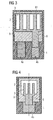
- the FIG. 3 shows a schematic plan view of another embodiment of the radiation-emitting device.
- a first contact structure 4a and a second contact structure 4b are arranged on the carrier 1, a first contact structure 4a and a second contact structure 4b are arranged.
- the radiation exit surface 3 of the semiconductor chip 2 is electrically conductively connected to the second contact structure 4b via the second contact layer 6.
- the arranged on the radiation exit surface 3 portion of the second contact layer 6 is formed in partial areas as contact webs 61 and in addition as a frame which connects the outer ends of the contact webs 61 with each other.
- the Semiconductor chip 2 homogeneously supplied with voltage.
- the semiconductor chip 2 is surrounded by the passivation layer 5.
- the passivation layer 5 also represents the base for the second contact layer 6, which is guided by the second contact structure 4b to the radiation exit surface 3.
- FIG. 4 shows an embodiment of the radiation-emitting device in the schematic plan view. This embodiment is characterized by having a symmetrical structure with respect to the broken line.
- the second contact layer 6 is again formed here on the radiation exit surface 3 of the semiconductor chip 2 as contact webs 61.
- the symmetrical construction of the component ensures a particularly homogeneous voltage supply to the semiconductor chip 2, which leads to a particularly homogeneous emission characteristic of the semiconductor chip.
- Embodiment shown in each case there are also embodiments in which the radiation exit surface 3 is completely coated with the passivation layer 5 at least in the regions in which there are no webs or contact layers. For clarity, this is not shown in the figures. Thus, the semiconductor chip 2 is completely protected against environmental influences.
- the contact webs 61 are additionally provided with a passivation layer 5, so that the entire surface above the radiation exit surface 3 is provided with a passivation layer 5.
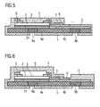
- the FIG. 5 shows an embodiment of the radiation-emitting device in the schematic side view.
- the carrier 1 has a first through-connection 8a and a second through-connection 8b.
- the first contact structure 4a or the second contact structure 4b can be contacted in an electrically conductive manner from the underside of the component.
- the second contact layer 6 is shaped like a frame in the region where it extends on the radiation exit surface 3 of the semiconductor chip 2.
- the radiation exit surface 3 is electrically conductively connected to the second contact structure 4b via the second contact layer.
- the entire component is completely encased by the passivation layer 5. Thus, the entire component is protected from environmental influences.
- This in FIG. 5 shown component is preferably formed by means of the first and the second via 8a, 8b as a surface mountable device.
- the schematic side view illustrated embodiment has a similar structure, as the embodiment, which in FIG. 5 is shown.
- the optical element 9 is in the in FIG. 6 illustrated embodiment by a conversion layer.
- This conversion layer 9 can comprise, for example, a converting substance, by means of which the radiation emitted by the semiconductor chip 2 or only wavelength ranges of this radiation in its Wavelength is modified. This can be done, for example, by absorbing the radiation emitted by the semiconductor chip 2 from the conversion substance and by emitting a radiation having a different wavelength from the conversion substance than the radiation which was absorbed by the conversion substance.
- the entire radiation emitted by the semiconductor chip 2 passes through the optical element 9.
- FIG. 7a illustrated embodiment has a similar structure, as the embodiment which in FIG. 5 is shown.
- embodiment shown additionally has an optical element 9.
- On the radiation exit surface 3 is a compensation layer 15 on which the optical element 9 is arranged.
- the leveling layer 15 can be used inter alia for planarizing the surface of the radiation exit surface 3.
- the upper surface of the optical element 9, ie the surface which faces away from the semiconductor chip 2, is likewise provided with a passivation layer 5.
- the optical element 9 is a pyramid filter in this embodiment.
- the passivation layer 5 can also have a uniform layer thickness in the region in which it runs on the pyramid filters. With the aid of these filters, the radiation emitted by the semiconductor chip 2 can be deflected in its spatial direction.
- FIG. 7b illustrated embodiment corresponds to the embodiment as shown in Figure 7a
- a passive component 100 is included.
- This passive component 100 is arranged on the second contact structure and also entirely from the Passivation layer 5 enclosed.
- the passive device 100 may be, for example, a protective diode or a resistor.
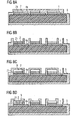
- FIG. 8a In the figure sequence 8a to 8d, three radiation-emitting components are shown in different process stages.
- a first contact structure 4a is arranged on the carrier 1, and a semiconductor chip 2, which is connected both mechanically and electrically conductively via the first contact layer 21 to the first contact structure 4a.
- the entire carrier 1 and the three components are each completely surrounded by the passivation layer 5.
- the passivation layer 5 has been exposed above the semiconductor chip 2 and above the first contact structure 4a in a partial region on which no first contact layer 21 is arranged.
- the removal of the passivation layer 5 can be carried out, for example, by means of RIE plasma etching ("reactive ion etching") with a fluorinated gas (for example NF 3 , CHF 3 , CF 4 or SF 6 ).
- an optical element 9 has been applied to the semiconductor chip 2.
- the optical element 9 is a conversion layer in this embodiment.
- the application of the conversion layer can in this case be carried out, for example, by means of platelets which comprise a converter material.
- the thickness of the conversion layer can be, for example, 20 ⁇ m.
- the thickness would be, for example, 100 microns.
- a portion of the passivation layer 5 which extends over the optical element 9 has been removed again.
- This removal of the passivation layer can be carried out, for example, by means of RIE plasma etching ("reactive ion etching") with a fluorinated gas.
- RIE plasma etching reactive ion etching
- fluorinated gas By exposing the optical element 9, the absorption of the emitted radiation can be reduced.
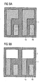
- FIGS. 9a to 9d an exemplary embodiment of the radiation-emitting component in four different process stages is shown schematically in plan view.
- FIG. 9a shows the carrier 1 on which in each case for two radiation-emitting components, the first contact structure 4a and the second contact structure 4b are shown.
- FIG. 9b shows an embodiment which, for example, from in FIG. 9a illustrated components could be produced, which was applied to a portion of the first contact structure 4a each have a semiconductor chip 2.
- the application of the semiconductor chip 2 can be done for example by bonding, soldering or gluing.
- a first contact layer 21 may be arranged between the semiconductor chip 2 and the first contact structure 4a.
- the process step shown may be from the process step as in FIG. 9b is shown, in that a passivation layer 5 has been applied.
- the passivation layer 5 encloses the semiconductor chips 2 in each case.
- the passivation layer 5 can be deposited, for example, by means of chemical vapor deposition (CVD), preferably by means of plasma-assisted vapor deposition (PECVD).
- CVD chemical vapor deposition
- PECVD plasma-assisted vapor deposition
- process step corresponds to the embodiment, as shown in FIG. 2 is shown.
- this could be from the procedural stage as in FIG. 9c shown is emerge, characterized in that on each component in each case the second contact layer 6 has been applied.
- the second contact layer 6 is formed as contact webs 61 in the subregions in which it extends on the semiconductor chip 2.
Landscapes
- Chemical & Material Sciences (AREA)
- Computer Hardware Design (AREA)
- Microelectronics & Electronic Packaging (AREA)
- Power Engineering (AREA)
- Engineering & Computer Science (AREA)
- Chemical Kinetics & Catalysis (AREA)
- Health & Medical Sciences (AREA)
- Medicinal Chemistry (AREA)
- Polymers & Plastics (AREA)
- Organic Chemistry (AREA)
- Led Device Packages (AREA)
- Led Devices (AREA)
- Polyoxymethylene Polymers And Polymers With Carbon-To-Carbon Bonds (AREA)
- Electroluminescent Light Sources (AREA)
Applications Claiming Priority (2)
| Application Number | Priority Date | Filing Date | Title |
|---|---|---|---|
| DE102008057350A DE102008057350A1 (de) | 2008-11-14 | 2008-11-14 | Strahlungsemittierendes Bauelement und Verfahren zu dessen Herstellung |
| PCT/DE2009/001571 WO2010054628A2 (de) | 2008-11-14 | 2009-11-05 | Strahlungsemittierendes bauelement und verfahren zu dessen herstellung |
Publications (2)
| Publication Number | Publication Date |
|---|---|
| EP2347455A2 EP2347455A2 (de) | 2011-07-27 |
| EP2347455B1 true EP2347455B1 (de) | 2013-03-27 |
Family
ID=42105044
Family Applications (1)
| Application Number | Title | Priority Date | Filing Date |
|---|---|---|---|
| EP09771686A Active EP2347455B1 (de) | 2008-11-14 | 2009-11-05 | Strahlungsemittierendes bauelement und verfahren zu dessen herstellung |
Country Status (7)
Families Citing this family (14)
| Publication number | Priority date | Publication date | Assignee | Title |
|---|---|---|---|---|
| DE102010031732A1 (de) * | 2010-07-21 | 2012-01-26 | Osram Opto Semiconductors Gmbh | Optoelektronisches Bauelement |
| DE102010033963A1 (de) * | 2010-08-11 | 2012-02-16 | Osram Opto Semiconductors Gmbh | Optoelektronisches Bauelement und Verfahren zur Herstellung eines optoelektronischen Bauelements |
| US8653542B2 (en) * | 2011-01-13 | 2014-02-18 | Tsmc Solid State Lighting Ltd. | Micro-interconnects for light-emitting diodes |
| DE102011010504A1 (de) * | 2011-02-07 | 2012-08-09 | Osram Opto Semiconductors Gmbh | Optoelektrischer Halbleiterchip |
| DE102011013821B4 (de) | 2011-03-14 | 2024-05-23 | OSRAM Opto Semiconductors Gesellschaft mit beschränkter Haftung | Verfahren zur Herstellung zumindest eines optoelektronischen Halbleiterchips |
| DE102011113428A1 (de) | 2011-09-14 | 2013-03-14 | Osram Opto Semiconductors Gmbh | Optoelektronisches Bauelement |
| DE102012209325B4 (de) | 2012-06-01 | 2021-09-30 | OSRAM Opto Semiconductors Gesellschaft mit beschränkter Haftung | Optoelektronisches Modul |
| DE102012109083A1 (de) * | 2012-09-26 | 2014-03-27 | Osram Opto Semiconductors Gmbh | Optoelektronisches Bauelement und Verfahren zu dessen Herstellung |
| EP2830087A1 (en) * | 2013-07-26 | 2015-01-28 | Hamilton Sundstrand Corporation | Method for interconnection of electrical components on a substrate |
| DE102013110733A1 (de) * | 2013-09-27 | 2015-04-02 | Osram Opto Semiconductors Gmbh | Optoelektronisches Halbleiterbauelement und Verfahren zur Herstellung eines optoelektronischen Halbleiterbauelements |
| KR102311791B1 (ko) * | 2015-10-16 | 2021-10-08 | 한국전기연구원 | 아민계 폴리머를 포함한 다이오드 제조방법 |
| DE102017112223A1 (de) | 2017-06-02 | 2018-12-06 | Osram Opto Semiconductors Gmbh | Halbleiterlaser-Bauteil und Verfahren zur Herstellung eines Halbleiterlaser-Bauteils |
| CN107978613A (zh) * | 2017-12-15 | 2018-05-01 | 中芯集成电路(宁波)有限公司 | 半导体感光器件及其感光表面处理方法 |
| JP7463662B2 (ja) | 2019-07-10 | 2024-04-09 | 日亜化学工業株式会社 | 画像表示装置の製造方法および画像表示装置 |
Family Cites Families (21)
| Publication number | Priority date | Publication date | Assignee | Title |
|---|---|---|---|---|
| GB9018698D0 (en) * | 1990-08-24 | 1990-10-10 | Lynxvale Ltd | Semiconductive copolymers for use in electroluminescent devices |
| US5973337A (en) * | 1997-08-25 | 1999-10-26 | Motorola, Inc. | Ball grid device with optically transmissive coating |
| EP2169733B1 (de) | 1997-09-29 | 2017-07-19 | OSRAM Opto Semiconductors GmbH | Halbleiterlichtquelle |
| JP3641122B2 (ja) * | 1997-12-26 | 2005-04-20 | ローム株式会社 | 半導体発光素子、半導体発光モジュール、およびこれらの製造方法 |
| US20020017652A1 (en) | 2000-08-08 | 2002-02-14 | Stefan Illek | Semiconductor chip for optoelectronics |
| US6740906B2 (en) * | 2001-07-23 | 2004-05-25 | Cree, Inc. | Light emitting diodes including modifications for submount bonding |
| JP2003133589A (ja) * | 2001-10-23 | 2003-05-09 | Mitsubishi Cable Ind Ltd | GaN系半導体発光ダイオード |
| DE102004029412A1 (de) * | 2004-02-27 | 2005-10-13 | Osram Opto Semiconductors Gmbh | Strahlungsemittierender Halbleiterchip und Verfahren zur Herstellung eines solchen Halbleiterchips |
| CN101032034A (zh) * | 2004-06-30 | 2007-09-05 | 克里公司 | 用于封装发光器件的芯片级方法和芯片级封装的发光器件 |
| JP4457826B2 (ja) * | 2004-09-22 | 2010-04-28 | 三菱化学株式会社 | 窒化物半導体を用いた発光ダイオード |
| DE102004050371A1 (de) | 2004-09-30 | 2006-04-13 | Osram Opto Semiconductors Gmbh | Optoelektronisches Bauelement mit einer drahtlosen Kontaktierung |
| US8318519B2 (en) * | 2005-01-11 | 2012-11-27 | SemiLEDs Optoelectronics Co., Ltd. | Method for handling a semiconductor wafer assembly |
| JP4692053B2 (ja) * | 2005-04-15 | 2011-06-01 | セイコーエプソン株式会社 | 画像登録装置、画像確認方法、および画像プレビュープログラム |
| KR101047683B1 (ko) * | 2005-05-17 | 2011-07-08 | 엘지이노텍 주식회사 | 와이어 본딩이 불필요한 발광소자 패키징 방법 |
| CN100480168C (zh) * | 2005-07-07 | 2009-04-22 | 上海交通大学 | 反应离子深刻蚀加工微结构的侧壁钝化方法 |
| DE102005063106A1 (de) * | 2005-12-30 | 2007-07-05 | Patent-Treuhand-Gesellschaft für elektrische Glühlampen mbH | Optoelektronischer Halbleiterchip und optoelektronisches Bauelement mit solch einem Halbleiterchip |
| JP4203087B2 (ja) * | 2006-07-25 | 2008-12-24 | 株式会社沖データ | 半導体複合装置、ledプリントヘッド及び画像形成装置 |
| US8207524B2 (en) * | 2006-08-04 | 2012-06-26 | Mitsubishi Chemical Corporation | Insulating layer, electronic device, field effect transistor, and polyvinylthiophenol |
| DE102006045702A1 (de) * | 2006-09-27 | 2008-04-03 | Osram Opto Semiconductors Gmbh | Optoelektronisches Bauteil |
| JP4846506B2 (ja) * | 2006-10-10 | 2011-12-28 | 株式会社フジクラ | 発光装置およびその製造方法 |
| JP5329404B2 (ja) * | 2007-06-21 | 2013-10-30 | 出光興産株式会社 | 有機薄膜トランジスタ及び有機薄膜発光トランジスタ |
-
2008
- 2008-11-14 DE DE102008057350A patent/DE102008057350A1/de not_active Withdrawn
-
2009
- 2009-11-05 WO PCT/DE2009/001571 patent/WO2010054628A2/de active Application Filing
- 2009-11-05 CN CN2009801452234A patent/CN102216365B/zh active Active
- 2009-11-05 EP EP09771686A patent/EP2347455B1/de active Active
- 2009-11-05 US US13/129,018 patent/US8552459B2/en active Active
- 2009-11-05 JP JP2011535870A patent/JP5538416B2/ja active Active
- 2009-11-05 KR KR1020117013636A patent/KR101609012B1/ko active Active
Also Published As
| Publication number | Publication date |
|---|---|
| US8552459B2 (en) | 2013-10-08 |
| WO2010054628A2 (de) | 2010-05-20 |
| JP5538416B2 (ja) | 2014-07-02 |
| CN102216365B (zh) | 2013-07-03 |
| EP2347455A2 (de) | 2011-07-27 |
| JP2012508971A (ja) | 2012-04-12 |
| KR20110095342A (ko) | 2011-08-24 |
| WO2010054628A3 (de) | 2010-12-23 |
| CN102216365A (zh) | 2011-10-12 |
| DE102008057350A1 (de) | 2010-05-20 |
| US20110278621A1 (en) | 2011-11-17 |
| KR101609012B1 (ko) | 2016-04-04 |
Similar Documents
| Publication | Publication Date | Title |
|---|---|---|
| EP2347455B1 (de) | Strahlungsemittierendes bauelement und verfahren zu dessen herstellung | |
| EP2638575B1 (de) | Optoelektronischer halbleiterchip und verfahren zu dessen herstellung | |
| EP2002176B1 (de) | Optoelektronischer frontscheinwerfer | |
| EP2149160B1 (de) | Optoelektronisches bauelement und verfahren zur herstellung einer mehrzahl optoelektronischer bauelemente | |
| DE102010034665B4 (de) | Optoelektronischer Halbleiterchip und Verfahren zur Herstellung von optoelektronischen Halbleiterchips | |
| EP2559076B1 (de) | Leuchtdiodenchip mit stromaufweitungsschicht | |
| EP2340568B1 (de) | Optoelektronischer halbleiterkörper | |
| DE102010031945A1 (de) | Halbleiterbauelement und Verfahren zur Herstellung eines Halbleiterbauelements | |
| DE202013012818U1 (de) | Linse und lichtemittierendes Modul zur Flächenbeleuchtung | |
| DE102007019775A1 (de) | Optoelektronisches Bauelement | |
| DE102015107586B4 (de) | Verfahren zur Herstellung optoelektronischer Bauelemente und oberflächenmontierbares optoelektronisches Bauelement | |
| WO2016156329A1 (de) | Optoelektronischer halbleiterchip, optoelektronisches halbleiterbauelement und verfahren zur herstellung eines optoelektronischen halbleiterchips | |
| DE102007046348A1 (de) | Strahlungsemittierendes Bauelement mit Glasabdeckung und Verfahren zu dessen Herstellung | |
| DE102008028886B4 (de) | Strahlungsemittierendes Bauelement und Verfahren zur Herstellung eines strahlungsemittierenden Bauelements | |
| DE102015107588B4 (de) | Verfahren zur Herstellung optoelektronischer Bauelemente und oberflächenmontierbares optoelektronisches Bauelement | |
| DE102014108373A1 (de) | Optoelektronischer Halbleiterchip | |
| WO2014170211A1 (de) | Optoelektronisches bauelement | |
| DE102015107593A1 (de) | Optoelektronischer Halbleiterchip und Leuchtmittel | |
| WO2019020424A1 (de) | Optoelektronischer halbleiterchip, hochvolthalbleiterchip und verfahren zur herstellung eines optoelektronischen halbleiterchips | |
| EP2304816B1 (de) | Elektrolumineszierende vorrichtung und verfahren zur herstellung einer elektrolumineszierenden vorrichtung | |
| DE102019106546A1 (de) | Verfahren zur herstellung von optoelektronischen halbleiterbauteilen und optoelektronisches halbleiterbauteil | |
| WO2022248247A1 (de) | Optoelektronisches halbleiterbauteil und paneel | |
| EP2619807B1 (de) | Optoelektronischer halbleiterchip und verfahren zu dessen herstellung | |
| DE102004047061B4 (de) | Optoelektronisches Bauelement und Verfahren zum Herstellen eines optoelektronischen Bauelements | |
| DE102015107591B4 (de) | Optoelektronisches Halbleiterbauteil und Verfahren zur Herstellung eines optoelektronischen Halbleiterbauteils |
Legal Events
| Date | Code | Title | Description |
|---|---|---|---|
| PUAI | Public reference made under article 153(3) epc to a published international application that has entered the european phase |
Free format text: ORIGINAL CODE: 0009012 |
|
| 17P | Request for examination filed |
Effective date: 20110216 |
|
| AK | Designated contracting states |
Kind code of ref document: A2 Designated state(s): AT BE BG CH CY CZ DE DK EE ES FI FR GB GR HR HU IE IS IT LI LT LU LV MC MK MT NL NO PL PT RO SE SI SK SM TR |
|
| AX | Request for extension of the european patent |
Extension state: AL BA RS |
|
| DAX | Request for extension of the european patent (deleted) | ||
| REG | Reference to a national code |
Ref country code: DE Ref legal event code: R079 Ref document number: 502009006672 Country of ref document: DE Free format text: PREVIOUS MAIN CLASS: H01L0033560000 Ipc: H01L0033440000 |
|
| RIC1 | Information provided on ipc code assigned before grant |
Ipc: C08G 61/10 20060101ALI20120404BHEP Ipc: C08G 61/02 20060101ALI20120404BHEP Ipc: H01L 31/02 20060101ALI20120404BHEP Ipc: H01L 33/44 20100101AFI20120404BHEP Ipc: H01L 31/0216 20060101ALI20120404BHEP |
|
| GRAP | Despatch of communication of intention to grant a patent |
Free format text: ORIGINAL CODE: EPIDOSNIGR1 |
|
| GRAS | Grant fee paid |
Free format text: ORIGINAL CODE: EPIDOSNIGR3 |
|
| GRAA | (expected) grant |
Free format text: ORIGINAL CODE: 0009210 |
|
| AK | Designated contracting states |
Kind code of ref document: B1 Designated state(s): AT BE BG CH CY CZ DE DK EE ES FI FR GB GR HR HU IE IS IT LI LT LU LV MC MK MT NL NO PL PT RO SE SI SK SM TR |
|
| REG | Reference to a national code |
Ref country code: GB Ref legal event code: FG4D Free format text: NOT ENGLISH |
|
| REG | Reference to a national code |
Ref country code: CH Ref legal event code: EP |
|
| REG | Reference to a national code |
Ref country code: AT Ref legal event code: REF Ref document number: 603903 Country of ref document: AT Kind code of ref document: T Effective date: 20130415 |
|
| REG | Reference to a national code |
Ref country code: IE Ref legal event code: FG4D Free format text: LANGUAGE OF EP DOCUMENT: GERMAN |
|
| REG | Reference to a national code |
Ref country code: DE Ref legal event code: R096 Ref document number: 502009006672 Country of ref document: DE Effective date: 20130523 |
|
| PG25 | Lapsed in a contracting state [announced via postgrant information from national office to epo] |
Ref country code: BG Free format text: LAPSE BECAUSE OF FAILURE TO SUBMIT A TRANSLATION OF THE DESCRIPTION OR TO PAY THE FEE WITHIN THE PRESCRIBED TIME-LIMIT Effective date: 20130627 Ref country code: SE Free format text: LAPSE BECAUSE OF FAILURE TO SUBMIT A TRANSLATION OF THE DESCRIPTION OR TO PAY THE FEE WITHIN THE PRESCRIBED TIME-LIMIT Effective date: 20130327 Ref country code: NO Free format text: LAPSE BECAUSE OF FAILURE TO SUBMIT A TRANSLATION OF THE DESCRIPTION OR TO PAY THE FEE WITHIN THE PRESCRIBED TIME-LIMIT Effective date: 20130627 Ref country code: LT Free format text: LAPSE BECAUSE OF FAILURE TO SUBMIT A TRANSLATION OF THE DESCRIPTION OR TO PAY THE FEE WITHIN THE PRESCRIBED TIME-LIMIT Effective date: 20130327 |
|
| REG | Reference to a national code |
Ref country code: LT Ref legal event code: MG4D |
|
| PG25 | Lapsed in a contracting state [announced via postgrant information from national office to epo] |
Ref country code: FI Free format text: LAPSE BECAUSE OF FAILURE TO SUBMIT A TRANSLATION OF THE DESCRIPTION OR TO PAY THE FEE WITHIN THE PRESCRIBED TIME-LIMIT Effective date: 20130327 Ref country code: LV Free format text: LAPSE BECAUSE OF FAILURE TO SUBMIT A TRANSLATION OF THE DESCRIPTION OR TO PAY THE FEE WITHIN THE PRESCRIBED TIME-LIMIT Effective date: 20130327 Ref country code: SI Free format text: LAPSE BECAUSE OF FAILURE TO SUBMIT A TRANSLATION OF THE DESCRIPTION OR TO PAY THE FEE WITHIN THE PRESCRIBED TIME-LIMIT Effective date: 20130327 Ref country code: GR Free format text: LAPSE BECAUSE OF FAILURE TO SUBMIT A TRANSLATION OF THE DESCRIPTION OR TO PAY THE FEE WITHIN THE PRESCRIBED TIME-LIMIT Effective date: 20130628 |
|
| REG | Reference to a national code |
Ref country code: NL Ref legal event code: VDEP Effective date: 20130327 |
|
| PG25 | Lapsed in a contracting state [announced via postgrant information from national office to epo] |
Ref country code: HR Free format text: LAPSE BECAUSE OF FAILURE TO SUBMIT A TRANSLATION OF THE DESCRIPTION OR TO PAY THE FEE WITHIN THE PRESCRIBED TIME-LIMIT Effective date: 20130327 |
|
| PG25 | Lapsed in a contracting state [announced via postgrant information from national office to epo] |
Ref country code: RO Free format text: LAPSE BECAUSE OF FAILURE TO SUBMIT A TRANSLATION OF THE DESCRIPTION OR TO PAY THE FEE WITHIN THE PRESCRIBED TIME-LIMIT Effective date: 20130327 Ref country code: PT Free format text: LAPSE BECAUSE OF FAILURE TO SUBMIT A TRANSLATION OF THE DESCRIPTION OR TO PAY THE FEE WITHIN THE PRESCRIBED TIME-LIMIT Effective date: 20130729 Ref country code: IS Free format text: LAPSE BECAUSE OF FAILURE TO SUBMIT A TRANSLATION OF THE DESCRIPTION OR TO PAY THE FEE WITHIN THE PRESCRIBED TIME-LIMIT Effective date: 20130727 Ref country code: EE Free format text: LAPSE BECAUSE OF FAILURE TO SUBMIT A TRANSLATION OF THE DESCRIPTION OR TO PAY THE FEE WITHIN THE PRESCRIBED TIME-LIMIT Effective date: 20130327 Ref country code: SK Free format text: LAPSE BECAUSE OF FAILURE TO SUBMIT A TRANSLATION OF THE DESCRIPTION OR TO PAY THE FEE WITHIN THE PRESCRIBED TIME-LIMIT Effective date: 20130327 Ref country code: NL Free format text: LAPSE BECAUSE OF FAILURE TO SUBMIT A TRANSLATION OF THE DESCRIPTION OR TO PAY THE FEE WITHIN THE PRESCRIBED TIME-LIMIT Effective date: 20130327 Ref country code: ES Free format text: LAPSE BECAUSE OF FAILURE TO SUBMIT A TRANSLATION OF THE DESCRIPTION OR TO PAY THE FEE WITHIN THE PRESCRIBED TIME-LIMIT Effective date: 20130708 Ref country code: CZ Free format text: LAPSE BECAUSE OF FAILURE TO SUBMIT A TRANSLATION OF THE DESCRIPTION OR TO PAY THE FEE WITHIN THE PRESCRIBED TIME-LIMIT Effective date: 20130327 |
|
| PG25 | Lapsed in a contracting state [announced via postgrant information from national office to epo] |
Ref country code: PL Free format text: LAPSE BECAUSE OF FAILURE TO SUBMIT A TRANSLATION OF THE DESCRIPTION OR TO PAY THE FEE WITHIN THE PRESCRIBED TIME-LIMIT Effective date: 20130327 Ref country code: CY Free format text: LAPSE BECAUSE OF FAILURE TO SUBMIT A TRANSLATION OF THE DESCRIPTION OR TO PAY THE FEE WITHIN THE PRESCRIBED TIME-LIMIT Effective date: 20130327 |
|
| PG25 | Lapsed in a contracting state [announced via postgrant information from national office to epo] |
Ref country code: DK Free format text: LAPSE BECAUSE OF FAILURE TO SUBMIT A TRANSLATION OF THE DESCRIPTION OR TO PAY THE FEE WITHIN THE PRESCRIBED TIME-LIMIT Effective date: 20130327 |
|
| PLBE | No opposition filed within time limit |
Free format text: ORIGINAL CODE: 0009261 |
|
| STAA | Information on the status of an ep patent application or granted ep patent |
Free format text: STATUS: NO OPPOSITION FILED WITHIN TIME LIMIT |
|
| PG25 | Lapsed in a contracting state [announced via postgrant information from national office to epo] |
Ref country code: IT Free format text: LAPSE BECAUSE OF FAILURE TO SUBMIT A TRANSLATION OF THE DESCRIPTION OR TO PAY THE FEE WITHIN THE PRESCRIBED TIME-LIMIT Effective date: 20130327 |
|
| 26N | No opposition filed |
Effective date: 20140103 |
|
| REG | Reference to a national code |
Ref country code: DE Ref legal event code: R097 Ref document number: 502009006672 Country of ref document: DE Effective date: 20140103 |
|
| BERE | Be: lapsed |
Owner name: OSRAM OPTO SEMICONDUCTORS G.M.B.H. Effective date: 20131130 |
|
| REG | Reference to a national code |
Ref country code: CH Ref legal event code: PL |
|
| PG25 | Lapsed in a contracting state [announced via postgrant information from national office to epo] |
Ref country code: MC Free format text: LAPSE BECAUSE OF FAILURE TO SUBMIT A TRANSLATION OF THE DESCRIPTION OR TO PAY THE FEE WITHIN THE PRESCRIBED TIME-LIMIT Effective date: 20130327 Ref country code: CH Free format text: LAPSE BECAUSE OF NON-PAYMENT OF DUE FEES Effective date: 20131130 Ref country code: LI Free format text: LAPSE BECAUSE OF NON-PAYMENT OF DUE FEES Effective date: 20131130 |
|
| REG | Reference to a national code |
Ref country code: IE Ref legal event code: MM4A |
|
| PG25 | Lapsed in a contracting state [announced via postgrant information from national office to epo] |
Ref country code: BE Free format text: LAPSE BECAUSE OF NON-PAYMENT OF DUE FEES Effective date: 20131130 |
|
| PG25 | Lapsed in a contracting state [announced via postgrant information from national office to epo] |
Ref country code: IE Free format text: LAPSE BECAUSE OF NON-PAYMENT OF DUE FEES Effective date: 20131105 |
|
| PG25 | Lapsed in a contracting state [announced via postgrant information from national office to epo] |
Ref country code: SM Free format text: LAPSE BECAUSE OF FAILURE TO SUBMIT A TRANSLATION OF THE DESCRIPTION OR TO PAY THE FEE WITHIN THE PRESCRIBED TIME-LIMIT Effective date: 20130327 |
|
| PG25 | Lapsed in a contracting state [announced via postgrant information from national office to epo] |
Ref country code: TR Free format text: LAPSE BECAUSE OF FAILURE TO SUBMIT A TRANSLATION OF THE DESCRIPTION OR TO PAY THE FEE WITHIN THE PRESCRIBED TIME-LIMIT Effective date: 20130327 |
|
| PG25 | Lapsed in a contracting state [announced via postgrant information from national office to epo] |
Ref country code: MK Free format text: LAPSE BECAUSE OF FAILURE TO SUBMIT A TRANSLATION OF THE DESCRIPTION OR TO PAY THE FEE WITHIN THE PRESCRIBED TIME-LIMIT Effective date: 20130327 Ref country code: LU Free format text: LAPSE BECAUSE OF NON-PAYMENT OF DUE FEES Effective date: 20131105 Ref country code: HU Free format text: LAPSE BECAUSE OF FAILURE TO SUBMIT A TRANSLATION OF THE DESCRIPTION OR TO PAY THE FEE WITHIN THE PRESCRIBED TIME-LIMIT; INVALID AB INITIO Effective date: 20091105 |
|
| PG25 | Lapsed in a contracting state [announced via postgrant information from national office to epo] |
Ref country code: MT Free format text: LAPSE BECAUSE OF FAILURE TO SUBMIT A TRANSLATION OF THE DESCRIPTION OR TO PAY THE FEE WITHIN THE PRESCRIBED TIME-LIMIT Effective date: 20130327 |
|
| REG | Reference to a national code |
Ref country code: FR Ref legal event code: PLFP Year of fee payment: 7 |
|
| REG | Reference to a national code |
Ref country code: AT Ref legal event code: MM01 Ref document number: 603903 Country of ref document: AT Kind code of ref document: T Effective date: 20141105 |
|
| PG25 | Lapsed in a contracting state [announced via postgrant information from national office to epo] |
Ref country code: AT Free format text: LAPSE BECAUSE OF NON-PAYMENT OF DUE FEES Effective date: 20141105 |
|
| REG | Reference to a national code |
Ref country code: FR Ref legal event code: PLFP Year of fee payment: 8 |
|
| REG | Reference to a national code |
Ref country code: FR Ref legal event code: PLFP Year of fee payment: 9 |
|
| P01 | Opt-out of the competence of the unified patent court (upc) registered |
Effective date: 20230825 |
|
| REG | Reference to a national code |
Ref country code: DE Ref legal event code: R079 Ref document number: 502009006672 Country of ref document: DE Free format text: PREVIOUS MAIN CLASS: H01L0033440000 Ipc: H10H0020840000 |
|
| PGFP | Annual fee paid to national office [announced via postgrant information from national office to epo] |
Ref country code: DE Payment date: 20241121 Year of fee payment: 16 |
|
| PGFP | Annual fee paid to national office [announced via postgrant information from national office to epo] |
Ref country code: GB Payment date: 20241120 Year of fee payment: 16 |
|
| PGFP | Annual fee paid to national office [announced via postgrant information from national office to epo] |
Ref country code: FR Payment date: 20241128 Year of fee payment: 16 |