EP2344611B1 - Benzimidazole compounds and organic photoelectric device with the same - Google Patents
Benzimidazole compounds and organic photoelectric device with the same Download PDFInfo
- Publication number
- EP2344611B1 EP2344611B1 EP09820757.4A EP09820757A EP2344611B1 EP 2344611 B1 EP2344611 B1 EP 2344611B1 EP 09820757 A EP09820757 A EP 09820757A EP 2344611 B1 EP2344611 B1 EP 2344611B1
- Authority
- EP
- European Patent Office
- Prior art keywords
- organic
- layer
- photoelectric device
- organic photoelectric
- light emitting
- Prior art date
- Legal status (The legal status is an assumption and is not a legal conclusion. Google has not performed a legal analysis and makes no representation as to the accuracy of the status listed.)
- Active
Links
- 125000003785 benzimidazolyl group Chemical class N1=C(NC2=C1C=CC=C2)* 0.000 title 1
- 239000000463 material Substances 0.000 claims description 66
- -1 benzimidazole compound Chemical class 0.000 claims description 31
- 230000000903 blocking effect Effects 0.000 claims description 15
- 238000002347 injection Methods 0.000 claims description 6
- 239000007924 injection Substances 0.000 claims description 6
- 239000000126 substance Substances 0.000 claims description 5
- 239000010410 layer Substances 0.000 description 91
- YMWUJEATGCHHMB-UHFFFAOYSA-N Dichloromethane Chemical compound ClCCl YMWUJEATGCHHMB-UHFFFAOYSA-N 0.000 description 57
- 239000000243 solution Substances 0.000 description 20
- 230000005525 hole transport Effects 0.000 description 18
- 239000002904 solvent Substances 0.000 description 18
- 0 C1C2(c3ccccc3)c(cccc3)c3-c3cc(-c4cc(-c5nc(cccc6)c6[n]5)cc(-c5cccc(C6C=CC([n]7c8ccccc8c8c7cccc8)=CC6)n5)c4)ccc3*12 Chemical compound C1C2(c3ccccc3)c(cccc3)c3-c3cc(-c4cc(-c5nc(cccc6)c6[n]5)cc(-c5cccc(C6C=CC([n]7c8ccccc8c8c7cccc8)=CC6)n5)c4)ccc3*12 0.000 description 16
- WYURNTSHIVDZCO-UHFFFAOYSA-N Tetrahydrofuran Chemical compound C1CCOC1 WYURNTSHIVDZCO-UHFFFAOYSA-N 0.000 description 16
- 238000000034 method Methods 0.000 description 14
- 239000000376 reactant Substances 0.000 description 14
- 230000000052 comparative effect Effects 0.000 description 13
- IAZDPXIOMUYVGZ-UHFFFAOYSA-N Dimethylsulphoxide Chemical compound CS(C)=O IAZDPXIOMUYVGZ-UHFFFAOYSA-N 0.000 description 12
- 150000001875 compounds Chemical class 0.000 description 12
- 239000000758 substrate Substances 0.000 description 12
- UJOBWOGCFQCDNV-UHFFFAOYSA-N 9H-carbazole Chemical compound C1=CC=C2C3=CC=CC=C3NC2=C1 UJOBWOGCFQCDNV-UHFFFAOYSA-N 0.000 description 11
- 230000015572 biosynthetic process Effects 0.000 description 11
- 230000008859 change Effects 0.000 description 11
- 230000008569 process Effects 0.000 description 11
- 238000003786 synthesis reaction Methods 0.000 description 11
- 239000010409 thin film Substances 0.000 description 11
- 238000005259 measurement Methods 0.000 description 10
- XLYOFNOQVPJJNP-UHFFFAOYSA-N water Substances O XLYOFNOQVPJJNP-UHFFFAOYSA-N 0.000 description 10
- CSNNHWWHGAXBCP-UHFFFAOYSA-L Magnesium sulfate Chemical compound [Mg+2].[O-][S+2]([O-])([O-])[O-] CSNNHWWHGAXBCP-UHFFFAOYSA-L 0.000 description 9
- 238000006243 chemical reaction Methods 0.000 description 9
- 229920000642 polymer Polymers 0.000 description 9
- VYPSYNLAJGMNEJ-UHFFFAOYSA-N Silicium dioxide Chemical compound O=[Si]=O VYPSYNLAJGMNEJ-UHFFFAOYSA-N 0.000 description 8
- 239000012300 argon atmosphere Substances 0.000 description 8
- 238000010992 reflux Methods 0.000 description 8
- 239000000741 silica gel Substances 0.000 description 8
- 229910002027 silica gel Inorganic materials 0.000 description 8
- 239000007787 solid Substances 0.000 description 8
- YLQBMQCUIZJEEH-UHFFFAOYSA-N tetrahydrofuran Natural products C=1C=COC=1 YLQBMQCUIZJEEH-UHFFFAOYSA-N 0.000 description 8
- TVIVIEFSHFOWTE-UHFFFAOYSA-K tri(quinolin-8-yloxy)alumane Chemical compound [Al+3].C1=CN=C2C([O-])=CC=CC2=C1.C1=CN=C2C([O-])=CC=CC2=C1.C1=CN=C2C([O-])=CC=CC2=C1 TVIVIEFSHFOWTE-UHFFFAOYSA-K 0.000 description 8
- QTBSBXVTEAMEQO-UHFFFAOYSA-N Acetic acid Chemical compound CC(O)=O QTBSBXVTEAMEQO-UHFFFAOYSA-N 0.000 description 6
- ZUOUZKKEUPVFJK-UHFFFAOYSA-N diphenyl Chemical compound C1=CC=CC=C1C1=CC=CC=C1 ZUOUZKKEUPVFJK-UHFFFAOYSA-N 0.000 description 6
- XLYOFNOQVPJJNP-UHFFFAOYSA-M hydroxide Chemical compound [OH-] XLYOFNOQVPJJNP-UHFFFAOYSA-M 0.000 description 6
- NFHFRUOZVGFOOS-UHFFFAOYSA-N palladium;triphenylphosphane Chemical compound [Pd].C1=CC=CC=C1P(C=1C=CC=CC=1)C1=CC=CC=C1.C1=CC=CC=C1P(C=1C=CC=CC=1)C1=CC=CC=C1.C1=CC=CC=C1P(C=1C=CC=CC=1)C1=CC=CC=C1.C1=CC=CC=C1P(C=1C=CC=CC=1)C1=CC=CC=C1 NFHFRUOZVGFOOS-UHFFFAOYSA-N 0.000 description 6
- 239000002019 doping agent Substances 0.000 description 5
- 230000005283 ground state Effects 0.000 description 5
- 239000000203 mixture Substances 0.000 description 5
- 230000003287 optical effect Effects 0.000 description 5
- 238000005424 photoluminescence Methods 0.000 description 5
- SPDPTFAJSFKAMT-UHFFFAOYSA-N 1-n-[4-[4-(n-[4-(3-methyl-n-(3-methylphenyl)anilino)phenyl]anilino)phenyl]phenyl]-4-n,4-n-bis(3-methylphenyl)-1-n-phenylbenzene-1,4-diamine Chemical compound CC1=CC=CC(N(C=2C=CC(=CC=2)N(C=2C=CC=CC=2)C=2C=CC(=CC=2)C=2C=CC(=CC=2)N(C=2C=CC=CC=2)C=2C=CC(=CC=2)N(C=2C=C(C)C=CC=2)C=2C=C(C)C=CC=2)C=2C=C(C)C=CC=2)=C1 SPDPTFAJSFKAMT-UHFFFAOYSA-N 0.000 description 4
- 238000000151 deposition Methods 0.000 description 4
- 238000005137 deposition process Methods 0.000 description 4
- 239000011521 glass Substances 0.000 description 4
- YERGTYJYQCLVDM-UHFFFAOYSA-N iridium(3+);2-(4-methylphenyl)pyridine Chemical compound [Ir+3].C1=CC(C)=CC=C1C1=CC=CC=N1.C1=CC(C)=CC=C1C1=CC=CC=N1.C1=CC(C)=CC=C1C1=CC=CC=N1 YERGTYJYQCLVDM-UHFFFAOYSA-N 0.000 description 4
- VLKZOEOYAKHREP-UHFFFAOYSA-N n-Hexane Chemical compound CCCCCC VLKZOEOYAKHREP-UHFFFAOYSA-N 0.000 description 4
- 150000002894 organic compounds Chemical class 0.000 description 4
- BWHMMNNQKKPAPP-UHFFFAOYSA-L potassium carbonate Chemical compound [K+].[K+].[O-]C([O-])=O BWHMMNNQKKPAPP-UHFFFAOYSA-L 0.000 description 4
- 229920005989 resin Polymers 0.000 description 4
- 239000011347 resin Substances 0.000 description 4
- 238000001771 vacuum deposition Methods 0.000 description 4
- VQGHOUODWALEFC-UHFFFAOYSA-N 2-phenylpyridine Chemical compound C1=CC=CC=C1C1=CC=CC=N1 VQGHOUODWALEFC-UHFFFAOYSA-N 0.000 description 3
- AWXGSYPUMWKTBR-UHFFFAOYSA-N 4-carbazol-9-yl-n,n-bis(4-carbazol-9-ylphenyl)aniline Chemical compound C12=CC=CC=C2C2=CC=CC=C2N1C1=CC=C(N(C=2C=CC(=CC=2)N2C3=CC=CC=C3C3=CC=CC=C32)C=2C=CC(=CC=2)N2C3=CC=CC=C3C3=CC=CC=C32)C=C1 AWXGSYPUMWKTBR-UHFFFAOYSA-N 0.000 description 3
- UHOVQNZJYSORNB-UHFFFAOYSA-N Benzene Chemical compound C1=CC=CC=C1 UHOVQNZJYSORNB-UHFFFAOYSA-N 0.000 description 3
- 101000837344 Homo sapiens T-cell leukemia translocation-altered gene protein Proteins 0.000 description 3
- 102100028692 T-cell leukemia translocation-altered gene protein Human genes 0.000 description 3
- 235000010290 biphenyl Nutrition 0.000 description 3
- 239000004305 biphenyl Substances 0.000 description 3
- UFVXQDWNSAGPHN-UHFFFAOYSA-K bis[(2-methylquinolin-8-yl)oxy]-(4-phenylphenoxy)alumane Chemical compound [Al+3].C1=CC=C([O-])C2=NC(C)=CC=C21.C1=CC=C([O-])C2=NC(C)=CC=C21.C1=CC([O-])=CC=C1C1=CC=CC=C1 UFVXQDWNSAGPHN-UHFFFAOYSA-K 0.000 description 3
- 239000011575 calcium Substances 0.000 description 3
- 150000004696 coordination complex Chemical class 0.000 description 3
- 238000004895 liquid chromatography mass spectrometry Methods 0.000 description 3
- 229910052751 metal Inorganic materials 0.000 description 3
- 239000002184 metal Substances 0.000 description 3
- 229910021645 metal ion Inorganic materials 0.000 description 3
- 229910052757 nitrogen Inorganic materials 0.000 description 3
- 239000012044 organic layer Substances 0.000 description 3
- 238000004528 spin coating Methods 0.000 description 3
- XOLBLPGZBRYERU-UHFFFAOYSA-N tin dioxide Chemical compound O=[Sn]=O XOLBLPGZBRYERU-UHFFFAOYSA-N 0.000 description 3
- UFWIBTONFRDIAS-UHFFFAOYSA-N Naphthalene Chemical compound C1=CC=CC2=CC=CC=C21 UFWIBTONFRDIAS-UHFFFAOYSA-N 0.000 description 2
- 229910052782 aluminium Inorganic materials 0.000 description 2
- XAGFODPZIPBFFR-UHFFFAOYSA-N aluminium Chemical compound [Al] XAGFODPZIPBFFR-UHFFFAOYSA-N 0.000 description 2
- MWPLVEDNUUSJAV-UHFFFAOYSA-N anthracene Chemical compound C1=CC=CC2=CC3=CC=CC=C3C=C21 MWPLVEDNUUSJAV-UHFFFAOYSA-N 0.000 description 2
- 150000001556 benzimidazoles Chemical class 0.000 description 2
- 239000011230 binding agent Substances 0.000 description 2
- WDECIBYCCFPHNR-UHFFFAOYSA-N chrysene Chemical compound C1=CC=CC2=CC=C3C4=CC=CC=C4C=CC3=C21 WDECIBYCCFPHNR-UHFFFAOYSA-N 0.000 description 2
- 238000000576 coating method Methods 0.000 description 2
- ORTQZVOHEJQUHG-UHFFFAOYSA-L copper(II) chloride Chemical compound Cl[Cu]Cl ORTQZVOHEJQUHG-UHFFFAOYSA-L 0.000 description 2
- 239000013078 crystal Substances 0.000 description 2
- 238000011156 evaluation Methods 0.000 description 2
- NIHNNTQXNPWCJQ-UHFFFAOYSA-N fluorene Chemical compound C1=CC=C2CC3=CC=CC=C3C2=C1 NIHNNTQXNPWCJQ-UHFFFAOYSA-N 0.000 description 2
- 125000005842 heteroatom Chemical group 0.000 description 2
- 230000005764 inhibitory process Effects 0.000 description 2
- 239000011229 interlayer Substances 0.000 description 2
- 229910052741 iridium Inorganic materials 0.000 description 2
- 239000007788 liquid Substances 0.000 description 2
- 229910052744 lithium Inorganic materials 0.000 description 2
- 239000011777 magnesium Substances 0.000 description 2
- 238000004519 manufacturing process Methods 0.000 description 2
- 239000012528 membrane Substances 0.000 description 2
- ZGEGCLOFRBLKSE-UHFFFAOYSA-N methylene hexane Natural products CCCCCC=C ZGEGCLOFRBLKSE-UHFFFAOYSA-N 0.000 description 2
- 239000012046 mixed solvent Substances 0.000 description 2
- 238000002156 mixing Methods 0.000 description 2
- YNPNZTXNASCQKK-UHFFFAOYSA-N phenanthrene Chemical compound C1=CC=C2C3=CC=CC=C3C=CC2=C1 YNPNZTXNASCQKK-UHFFFAOYSA-N 0.000 description 2
- 229910052697 platinum Inorganic materials 0.000 description 2
- 229920003227 poly(N-vinyl carbazole) Polymers 0.000 description 2
- 229920000172 poly(styrenesulfonic acid) Polymers 0.000 description 2
- 229910000027 potassium carbonate Inorganic materials 0.000 description 2
- BBEAQIROQSPTKN-UHFFFAOYSA-N pyrene Chemical compound C1=CC=C2C=CC3=CC=CC4=CC=C1C2=C43 BBEAQIROQSPTKN-UHFFFAOYSA-N 0.000 description 2
- 238000005215 recombination Methods 0.000 description 2
- 230000006798 recombination Effects 0.000 description 2
- 238000004544 sputter deposition Methods 0.000 description 2
- PJANXHGTPQOBST-VAWYXSNFSA-N trans-stilbene Chemical compound C=1C=CC=CC=1/C=C/C1=CC=CC=C1 PJANXHGTPQOBST-VAWYXSNFSA-N 0.000 description 2
- 150000005072 1,3,4-oxadiazoles Chemical class 0.000 description 1
- YJTKZCDBKVTVBY-UHFFFAOYSA-N 1,3-Diphenylbenzene Chemical group C1=CC=CC=C1C1=CC=CC(C=2C=CC=CC=2)=C1 YJTKZCDBKVTVBY-UHFFFAOYSA-N 0.000 description 1
- YQDSWSPIWVQKBC-UHFFFAOYSA-N 1h-cyclopenta[l]phenanthrene Chemical compound C12=CC=CC=C2C2=CC=CC=C2C2=C1CC=C2 YQDSWSPIWVQKBC-UHFFFAOYSA-N 0.000 description 1
- STTGYIUESPWXOW-UHFFFAOYSA-N 2,9-dimethyl-4,7-diphenyl-1,10-phenanthroline Chemical compound C=12C=CC3=C(C=4C=CC=CC=4)C=C(C)N=C3C2=NC(C)=CC=1C1=CC=CC=C1 STTGYIUESPWXOW-UHFFFAOYSA-N 0.000 description 1
- GEQBRULPNIVQPP-UHFFFAOYSA-N 2-[3,5-bis(1-phenylbenzimidazol-2-yl)phenyl]-1-phenylbenzimidazole Chemical compound C1=CC=CC=C1N1C2=CC=CC=C2N=C1C1=CC(C=2N(C3=CC=CC=C3N=2)C=2C=CC=CC=2)=CC(C=2N(C3=CC=CC=C3N=2)C=2C=CC=CC=2)=C1 GEQBRULPNIVQPP-UHFFFAOYSA-N 0.000 description 1
- NFCPRRWCTNLGSN-UHFFFAOYSA-N 2-n-phenylbenzene-1,2-diamine Chemical compound NC1=CC=CC=C1NC1=CC=CC=C1 NFCPRRWCTNLGSN-UHFFFAOYSA-N 0.000 description 1
- ZLDMZIXUGCGKMB-UHFFFAOYSA-N 3,5-dibromobenzaldehyde Chemical compound BrC1=CC(Br)=CC(C=O)=C1 ZLDMZIXUGCGKMB-UHFFFAOYSA-N 0.000 description 1
- MZWDAEVXPZRJTQ-WUXMJOGZSA-N 4-[(e)-(4-fluorophenyl)methylideneamino]-3-methyl-1h-1,2,4-triazole-5-thione Chemical compound CC1=NNC(=S)N1\N=C\C1=CC=C(F)C=C1 MZWDAEVXPZRJTQ-WUXMJOGZSA-N 0.000 description 1
- LLFGEXZJKGRDGN-UHFFFAOYSA-N 84849-89-8 Chemical compound C12=CC=CC=C2C2=CC=CC=C2C2=C1C1OC1C=C2 LLFGEXZJKGRDGN-UHFFFAOYSA-N 0.000 description 1
- YBSGMJKMJJPPOQ-UHFFFAOYSA-N BC[IH]c1cc(-c2nc3ccccc3[nH]2)cc(-c2cc(C)cc(-[n]3c(cccc4)c4c4c3cccc4)c2)c1 Chemical compound BC[IH]c1cc(-c2nc3ccccc3[nH]2)cc(-c2cc(C)cc(-[n]3c(cccc4)c4c4c3cccc4)c2)c1 YBSGMJKMJJPPOQ-UHFFFAOYSA-N 0.000 description 1
- FMMWHPNWAFZXNH-UHFFFAOYSA-N Benz[a]pyrene Chemical compound C1=C2C3=CC=CC=C3C=C(C=C3)C2=C2C3=CC=CC2=C1 FMMWHPNWAFZXNH-UHFFFAOYSA-N 0.000 description 1
- YFJRESIEBIPWRE-GBHKTEFQSA-N C([C@H]1C2C1c1ccccc1)c(ccc(-c1cc(-c(cc3)ccc3-[n]3c4ccccc4c4c3cccc4)cc(-c3nc(cccc4)c4[n]3-c3ccccc3)c1)c1)c1-c1c2cccc1 Chemical compound C([C@H]1C2C1c1ccccc1)c(ccc(-c1cc(-c(cc3)ccc3-[n]3c4ccccc4c4c3cccc4)cc(-c3nc(cccc4)c4[n]3-c3ccccc3)c1)c1)c1-c1c2cccc1 YFJRESIEBIPWRE-GBHKTEFQSA-N 0.000 description 1
- OUFLRYFGMJNDNH-UHFFFAOYSA-N C1C=CC([n]2c(-c(cc(cc3)-c4nc5ccccc5[n]4-c4ccccc4)c3-[n]3c(cccc4)c4c4c3cccc4)nc3c2cccc3)=CC=C1 Chemical compound C1C=CC([n]2c(-c(cc(cc3)-c4nc5ccccc5[n]4-c4ccccc4)c3-[n]3c(cccc4)c4c4c3cccc4)nc3c2cccc3)=CC=C1 OUFLRYFGMJNDNH-UHFFFAOYSA-N 0.000 description 1
- KSMLFRRDFPQPKZ-PEMGLXIVSA-N CB(/C(/C)=C/C([n]1c(cccc2)c2c(C)c1/C=C\NC)=C)OC(C)(C)C(C)(C)O Chemical compound CB(/C(/C)=C/C([n]1c(cccc2)c2c(C)c1/C=C\NC)=C)OC(C)(C)C(C)(C)O KSMLFRRDFPQPKZ-PEMGLXIVSA-N 0.000 description 1
- JQZREJDVMACLKA-FPLPWBNLSA-N CC(/C=C\c1c[nH]c2c1C=CCC2)[IH]C Chemical compound CC(/C=C\c1c[nH]c2c1C=CCC2)[IH]C JQZREJDVMACLKA-FPLPWBNLSA-N 0.000 description 1
- UOEJLVXMUZIKOS-UHFFFAOYSA-N CC(CC1)=CC=C1N(c1ccc(C)cc1)c1cc(N(c2ccc(C)cc2)c2ccc(C)cc2)cc(-c2nc(cccc3)c3[n]2-c2ccccc2)c1 Chemical compound CC(CC1)=CC=C1N(c1ccc(C)cc1)c1cc(N(c2ccc(C)cc2)c2ccc(C)cc2)cc(-c2nc(cccc3)c3[n]2-c2ccccc2)c1 UOEJLVXMUZIKOS-UHFFFAOYSA-N 0.000 description 1
- CUTINMXFRGYCRY-UHFFFAOYSA-N CC(CC=C1)C=[IH]1c1cc(-c2nc3ccccc3[nH]2)cc(-c2cc(-[n]3c4ccccc4c4c3cccc4)ccc2)c1 Chemical compound CC(CC=C1)C=[IH]1c1cc(-c2nc3ccccc3[nH]2)cc(-c2cc(-[n]3c4ccccc4c4c3cccc4)ccc2)c1 CUTINMXFRGYCRY-UHFFFAOYSA-N 0.000 description 1
- ORUVOPCUTZNTAK-UHFFFAOYSA-N CC1C=C(C)C=CC1 Chemical compound CC1C=C(C)C=CC1 ORUVOPCUTZNTAK-UHFFFAOYSA-N 0.000 description 1
- VRBLPAQJQHMGRJ-UHFFFAOYSA-N CC1c(cccc2)c2N(c2ccccc2)C(c2cc(-c(cc3)cc(c4c5cccc4)c3[n]5-c3ccccc3)cc(-c3cc(-[n]4c5ccccc5c5c4cccc5)ccc3)c2)=C1 Chemical compound CC1c(cccc2)c2N(c2ccccc2)C(c2cc(-c(cc3)cc(c4c5cccc4)c3[n]5-c3ccccc3)cc(-c3cc(-[n]4c5ccccc5c5c4cccc5)ccc3)c2)=C1 VRBLPAQJQHMGRJ-UHFFFAOYSA-N 0.000 description 1
- GCNMBVJSHITPIS-LURJTMIESA-N C[C@@H]1C=[I](C)=[I]C(C)=C1 Chemical compound C[C@@H]1C=[I](C)=[I]C(C)=C1 GCNMBVJSHITPIS-LURJTMIESA-N 0.000 description 1
- OYPRJOBELJOOCE-UHFFFAOYSA-N Calcium Chemical compound [Ca] OYPRJOBELJOOCE-UHFFFAOYSA-N 0.000 description 1
- ZKZZPKYJHUQTRW-UHFFFAOYSA-N Cc(cc1)ccc1N(c1ccc(C)cc1)c1cc(-c(cc2)ccc2-[n]2c3ccccc3c3c2cccc3)cc(-c(cc2)ccc2-c2nc3ccccc3[n]2-c2ccccc2)c1 Chemical compound Cc(cc1)ccc1N(c1ccc(C)cc1)c1cc(-c(cc2)ccc2-[n]2c3ccccc3c3c2cccc3)cc(-c(cc2)ccc2-c2nc3ccccc3[n]2-c2ccccc2)c1 ZKZZPKYJHUQTRW-UHFFFAOYSA-N 0.000 description 1
- JXDDAJJYNOGXSX-JBXBRNPSSA-N Cc(nc1-c2ccc(-c3cc(-[n]4c5ccccc5c5c4cccc5)cc(-[n]4c5ccccc5c5ccccc45)c3)c(-c3nc4ccccc4[n]3-c3ccccc3)c2)c(/C=C\C=C)[n]1-c1ccccc1 Chemical compound Cc(nc1-c2ccc(-c3cc(-[n]4c5ccccc5c5c4cccc5)cc(-[n]4c5ccccc5c5ccccc45)c3)c(-c3nc4ccccc4[n]3-c3ccccc3)c2)c(/C=C\C=C)[n]1-c1ccccc1 JXDDAJJYNOGXSX-JBXBRNPSSA-N 0.000 description 1
- DIJNLWQVWPTHFK-UHFFFAOYSA-N Cc1cc(-c2cccc(-c3cc(N)ccc3)n2)cc(-c2nc(cccc3)c3[n]2-c(cc2)c3-c2c3)c1 Chemical compound Cc1cc(-c2cccc(-c3cc(N)ccc3)n2)cc(-c2nc(cccc3)c3[n]2-c(cc2)c3-c2c3)c1 DIJNLWQVWPTHFK-UHFFFAOYSA-N 0.000 description 1
- PUZVUIDBBGIGMV-UHFFFAOYSA-N Cc1cc(Br)cc(-c2[n-]c(cccc3)c3[nH]2)c1 Chemical compound Cc1cc(Br)cc(-c2[n-]c(cccc3)c3[nH]2)c1 PUZVUIDBBGIGMV-UHFFFAOYSA-N 0.000 description 1
- FJXKHCXELURTAI-UHFFFAOYSA-N Cc1ccccc1-c1c(CCc2cc(-[n]3c4ccccc4c4c3cccc4)cc(-c3cc(-c4nc(cccc5)c5[n]4-c4ccccc4)cc(-c(cc4)ccc4-[n]4c5ccccc5c5c4cccc5)c3)c2)cccc1 Chemical compound Cc1ccccc1-c1c(CCc2cc(-[n]3c4ccccc4c4c3cccc4)cc(-c3cc(-c4nc(cccc5)c5[n]4-c4ccccc4)cc(-c(cc4)ccc4-[n]4c5ccccc5c5c4cccc5)c3)c2)cccc1 FJXKHCXELURTAI-UHFFFAOYSA-N 0.000 description 1
- 239000004641 Diallyl-phthalate Substances 0.000 description 1
- YCKRFDGAMUMZLT-UHFFFAOYSA-N Fluorine atom Chemical compound [F] YCKRFDGAMUMZLT-UHFFFAOYSA-N 0.000 description 1
- WHXSMMKQMYFTQS-UHFFFAOYSA-N Lithium Chemical compound [Li] WHXSMMKQMYFTQS-UHFFFAOYSA-N 0.000 description 1
- FYYHWMGAXLPEAU-UHFFFAOYSA-N Magnesium Chemical compound [Mg] FYYHWMGAXLPEAU-UHFFFAOYSA-N 0.000 description 1
- 229920000265 Polyparaphenylene Polymers 0.000 description 1
- 239000004793 Polystyrene Substances 0.000 description 1
- XBDYBAVJXHJMNQ-UHFFFAOYSA-N Tetrahydroanthracene Natural products C1=CC=C2C=C(CCCC3)C3=CC2=C1 XBDYBAVJXHJMNQ-UHFFFAOYSA-N 0.000 description 1
- 239000007983 Tris buffer Substances 0.000 description 1
- 229920001807 Urea-formaldehyde Polymers 0.000 description 1
- XLOMVQKBTHCTTD-UHFFFAOYSA-N Zinc monoxide Chemical compound [Zn]=O XLOMVQKBTHCTTD-UHFFFAOYSA-N 0.000 description 1
- 239000006096 absorbing agent Substances 0.000 description 1
- 125000000217 alkyl group Chemical group 0.000 description 1
- XEPMXWGXLQIFJN-UHFFFAOYSA-K aluminum;2-carboxyquinolin-8-olate Chemical compound [Al+3].C1=C(C([O-])=O)N=C2C(O)=CC=CC2=C1.C1=C(C([O-])=O)N=C2C(O)=CC=CC2=C1.C1=C(C([O-])=O)N=C2C(O)=CC=CC2=C1 XEPMXWGXLQIFJN-UHFFFAOYSA-K 0.000 description 1
- 238000004458 analytical method Methods 0.000 description 1
- 238000013459 approach Methods 0.000 description 1
- 150000004982 aromatic amines Chemical class 0.000 description 1
- 150000004984 aromatic diamines Chemical class 0.000 description 1
- 125000003118 aryl group Chemical group 0.000 description 1
- QUDWYFHPNIMBFC-UHFFFAOYSA-N bis(prop-2-enyl) benzene-1,2-dicarboxylate Chemical compound C=CCOC(=O)C1=CC=CC=C1C(=O)OCC=C QUDWYFHPNIMBFC-UHFFFAOYSA-N 0.000 description 1
- 239000000872 buffer Substances 0.000 description 1
- UYJLLMKMRZJRJE-UHFFFAOYSA-N c(cc1)ccc1-[n]1c(-c2cc(-[n]3c(cccc4)c4c4ccccc34)cc(-[n]3c4ccccc4c4c3cccc4)c2)nc2ccccc12 Chemical compound c(cc1)ccc1-[n]1c(-c2cc(-[n]3c(cccc4)c4c4ccccc34)cc(-[n]3c4ccccc4c4c3cccc4)c2)nc2ccccc12 UYJLLMKMRZJRJE-UHFFFAOYSA-N 0.000 description 1
- MTDMMGZGBDTQCL-UHFFFAOYSA-N c(cc1)ccc1-[n]1c(-c2cc(-c(cc3)ccc3-[n]3c(cccc4)c4c4ccccc34)cc(-c3nc(cccc4)c4[n]3-c3ccccc3)c2)nc2ccccc12 Chemical compound c(cc1)ccc1-[n]1c(-c2cc(-c(cc3)ccc3-[n]3c(cccc4)c4c4ccccc34)cc(-c3nc(cccc4)c4[n]3-c3ccccc3)c2)nc2ccccc12 MTDMMGZGBDTQCL-UHFFFAOYSA-N 0.000 description 1
- YADFQOWVHLQWHD-UHFFFAOYSA-N c(cc1)ccc1-[n]1c(-c2cc(-c3cccc(-c4cc(-[n]5c(cccc6)c6c6c5cccc6)ccc4)n3)cc(-[n]3c4ccccc4c4c3cccc4)c2)nc2ccccc12 Chemical compound c(cc1)ccc1-[n]1c(-c2cc(-c3cccc(-c4cc(-[n]5c(cccc6)c6c6c5cccc6)ccc4)n3)cc(-[n]3c4ccccc4c4c3cccc4)c2)nc2ccccc12 YADFQOWVHLQWHD-UHFFFAOYSA-N 0.000 description 1
- 229910052791 calcium Inorganic materials 0.000 description 1
- 150000001716 carbazoles Chemical class 0.000 description 1
- 125000003178 carboxy group Chemical group [H]OC(*)=O 0.000 description 1
- 239000010406 cathode material Substances 0.000 description 1
- 239000011248 coating agent Substances 0.000 description 1
- 239000003086 colorant Substances 0.000 description 1
- 239000004020 conductor Substances 0.000 description 1
- 125000004093 cyano group Chemical group *C#N 0.000 description 1
- 230000007547 defect Effects 0.000 description 1
- 230000001419 dependent effect Effects 0.000 description 1
- 150000004985 diamines Chemical class 0.000 description 1
- 239000003989 dielectric material Substances 0.000 description 1
- 230000000694 effects Effects 0.000 description 1
- 230000005684 electric field Effects 0.000 description 1
- 239000007772 electrode material Substances 0.000 description 1
- 239000012776 electronic material Substances 0.000 description 1
- 239000003822 epoxy resin Substances 0.000 description 1
- 230000005281 excited state Effects 0.000 description 1
- 239000010408 film Substances 0.000 description 1
- GVEPBJHOBDJJJI-UHFFFAOYSA-N fluoranthrene Natural products C1=CC(C2=CC=CC=C22)=C3C2=CC=CC3=C1 GVEPBJHOBDJJJI-UHFFFAOYSA-N 0.000 description 1
- 229910052731 fluorine Inorganic materials 0.000 description 1
- 239000011737 fluorine Substances 0.000 description 1
- 230000009477 glass transition Effects 0.000 description 1
- 229910052736 halogen Inorganic materials 0.000 description 1
- 150000002367 halogens Chemical class 0.000 description 1
- LNEPOXFFQSENCJ-UHFFFAOYSA-N haloperidol Chemical compound C1CC(O)(C=2C=CC(Cl)=CC=2)CCN1CCCC(=O)C1=CC=C(F)C=C1 LNEPOXFFQSENCJ-UHFFFAOYSA-N 0.000 description 1
- 125000001072 heteroaryl group Chemical group 0.000 description 1
- 125000002887 hydroxy group Chemical group [H]O* 0.000 description 1
- 125000002883 imidazolyl group Chemical group 0.000 description 1
- AMGQUBHHOARCQH-UHFFFAOYSA-N indium;oxotin Chemical compound [In].[Sn]=O AMGQUBHHOARCQH-UHFFFAOYSA-N 0.000 description 1
- 238000007641 inkjet printing Methods 0.000 description 1
- 229910052742 iron Inorganic materials 0.000 description 1
- 229940046892 lead acetate Drugs 0.000 description 1
- 239000004973 liquid crystal related substance Substances 0.000 description 1
- 125000000040 m-tolyl group Chemical group [H]C1=C([H])C(*)=C([H])C(=C1[H])C([H])([H])[H] 0.000 description 1
- 229910052749 magnesium Inorganic materials 0.000 description 1
- 238000004949 mass spectrometry Methods 0.000 description 1
- 230000007246 mechanism Effects 0.000 description 1
- 125000005641 methacryl group Chemical group 0.000 description 1
- 238000012986 modification Methods 0.000 description 1
- 230000004048 modification Effects 0.000 description 1
- 239000000178 monomer Substances 0.000 description 1
- 229910052759 nickel Inorganic materials 0.000 description 1
- 125000000449 nitro group Chemical group [O-][N+](*)=O 0.000 description 1
- 239000003960 organic solvent Substances 0.000 description 1
- 125000001181 organosilyl group Chemical group [SiH3]* 0.000 description 1
- 229910052762 osmium Inorganic materials 0.000 description 1
- 229910052760 oxygen Inorganic materials 0.000 description 1
- 229910052763 palladium Inorganic materials 0.000 description 1
- KDLHZDBZIXYQEI-UHFFFAOYSA-N palladium Substances [Pd] KDLHZDBZIXYQEI-UHFFFAOYSA-N 0.000 description 1
- 230000000737 periodic effect Effects 0.000 description 1
- 239000005011 phenolic resin Substances 0.000 description 1
- 125000001997 phenyl group Chemical group [H]C1=C([H])C([H])=C(*)C([H])=C1[H] 0.000 description 1
- PTMHPRAIXMAOOB-UHFFFAOYSA-N phosphoramidic acid Chemical compound NP(O)(O)=O PTMHPRAIXMAOOB-UHFFFAOYSA-N 0.000 description 1
- 229910052698 phosphorus Inorganic materials 0.000 description 1
- GBROPGWFBFCKAG-UHFFFAOYSA-N picene Chemical compound C1=CC2=C3C=CC=CC3=CC=C2C2=C1C1=CC=CC=C1C=C2 GBROPGWFBFCKAG-UHFFFAOYSA-N 0.000 description 1
- 229920003023 plastic Polymers 0.000 description 1
- 229920000553 poly(phenylenevinylene) Polymers 0.000 description 1
- 229920002492 poly(sulfone) Polymers 0.000 description 1
- 229920000515 polycarbonate Polymers 0.000 description 1
- 239000004417 polycarbonate Substances 0.000 description 1
- 229920000647 polyepoxide Polymers 0.000 description 1
- 229920000728 polyester Polymers 0.000 description 1
- 229920002223 polystyrene Polymers 0.000 description 1
- 125000002924 primary amino group Chemical group [H]N([H])* 0.000 description 1
- 125000004262 quinoxalin-2-yl group Chemical group [H]C1=NC2=C([H])C([H])=C([H])C([H])=C2N=C1* 0.000 description 1
- 125000001567 quinoxalinyl group Chemical class N1=C(C=NC2=CC=CC=C12)* 0.000 description 1
- 230000004044 response Effects 0.000 description 1
- 229910052703 rhodium Inorganic materials 0.000 description 1
- 229910052707 ruthenium Inorganic materials 0.000 description 1
- 229920002050 silicone resin Polymers 0.000 description 1
- 125000004469 siloxy group Chemical group [SiH3]O* 0.000 description 1
- 125000001424 substituent group Chemical group 0.000 description 1
- 229910052717 sulfur Inorganic materials 0.000 description 1
- 238000012360 testing method Methods 0.000 description 1
- IFLREYGFSNHWGE-UHFFFAOYSA-N tetracene Chemical compound C1=CC=CC2=CC3=CC4=CC=CC=C4C=C3C=C21 IFLREYGFSNHWGE-UHFFFAOYSA-N 0.000 description 1
- 229910001887 tin oxide Inorganic materials 0.000 description 1
- JFLKFZNIIQFQBS-FNCQTZNRSA-N trans,trans-1,4-Diphenyl-1,3-butadiene Chemical compound C=1C=CC=CC=1\C=C\C=C\C1=CC=CC=C1 JFLKFZNIIQFQBS-FNCQTZNRSA-N 0.000 description 1
- PJANXHGTPQOBST-UHFFFAOYSA-N trans-Stilbene Natural products C=1C=CC=CC=1C=CC1=CC=CC=C1 PJANXHGTPQOBST-UHFFFAOYSA-N 0.000 description 1
Images


Classifications
-
- C—CHEMISTRY; METALLURGY
- C07—ORGANIC CHEMISTRY
- C07D—HETEROCYCLIC COMPOUNDS
- C07D235/00—Heterocyclic compounds containing 1,3-diazole or hydrogenated 1,3-diazole rings, condensed with other rings
- C07D235/02—Heterocyclic compounds containing 1,3-diazole or hydrogenated 1,3-diazole rings, condensed with other rings condensed with carbocyclic rings or ring systems
- C07D235/04—Benzimidazoles; Hydrogenated benzimidazoles
- C07D235/06—Benzimidazoles; Hydrogenated benzimidazoles with only hydrogen atoms, hydrocarbon or substituted hydrocarbon radicals, directly attached in position 2
- C07D235/08—Radicals containing only hydrogen and carbon atoms
-
- C—CHEMISTRY; METALLURGY
- C07—ORGANIC CHEMISTRY
- C07D—HETEROCYCLIC COMPOUNDS
- C07D235/00—Heterocyclic compounds containing 1,3-diazole or hydrogenated 1,3-diazole rings, condensed with other rings
- C07D235/02—Heterocyclic compounds containing 1,3-diazole or hydrogenated 1,3-diazole rings, condensed with other rings condensed with carbocyclic rings or ring systems
- C07D235/04—Benzimidazoles; Hydrogenated benzimidazoles
- C07D235/18—Benzimidazoles; Hydrogenated benzimidazoles with aryl radicals directly attached in position 2
-
- C—CHEMISTRY; METALLURGY
- C07—ORGANIC CHEMISTRY
- C07D—HETEROCYCLIC COMPOUNDS
- C07D401/00—Heterocyclic compounds containing two or more hetero rings, having nitrogen atoms as the only ring hetero atoms, at least one ring being a six-membered ring with only one nitrogen atom
- C07D401/14—Heterocyclic compounds containing two or more hetero rings, having nitrogen atoms as the only ring hetero atoms, at least one ring being a six-membered ring with only one nitrogen atom containing three or more hetero rings
-
- C—CHEMISTRY; METALLURGY
- C07—ORGANIC CHEMISTRY
- C07D—HETEROCYCLIC COMPOUNDS
- C07D403/00—Heterocyclic compounds containing two or more hetero rings, having nitrogen atoms as the only ring hetero atoms, not provided for by group C07D401/00
- C07D403/02—Heterocyclic compounds containing two or more hetero rings, having nitrogen atoms as the only ring hetero atoms, not provided for by group C07D401/00 containing two hetero rings
- C07D403/08—Heterocyclic compounds containing two or more hetero rings, having nitrogen atoms as the only ring hetero atoms, not provided for by group C07D401/00 containing two hetero rings linked by a carbon chain containing alicyclic rings
-
- C—CHEMISTRY; METALLURGY
- C07—ORGANIC CHEMISTRY
- C07D—HETEROCYCLIC COMPOUNDS
- C07D403/00—Heterocyclic compounds containing two or more hetero rings, having nitrogen atoms as the only ring hetero atoms, not provided for by group C07D401/00
- C07D403/02—Heterocyclic compounds containing two or more hetero rings, having nitrogen atoms as the only ring hetero atoms, not provided for by group C07D401/00 containing two hetero rings
- C07D403/10—Heterocyclic compounds containing two or more hetero rings, having nitrogen atoms as the only ring hetero atoms, not provided for by group C07D401/00 containing two hetero rings linked by a carbon chain containing aromatic rings
-
- C—CHEMISTRY; METALLURGY
- C07—ORGANIC CHEMISTRY
- C07D—HETEROCYCLIC COMPOUNDS
- C07D403/00—Heterocyclic compounds containing two or more hetero rings, having nitrogen atoms as the only ring hetero atoms, not provided for by group C07D401/00
- C07D403/14—Heterocyclic compounds containing two or more hetero rings, having nitrogen atoms as the only ring hetero atoms, not provided for by group C07D401/00 containing three or more hetero rings
-
- C—CHEMISTRY; METALLURGY
- C09—DYES; PAINTS; POLISHES; NATURAL RESINS; ADHESIVES; COMPOSITIONS NOT OTHERWISE PROVIDED FOR; APPLICATIONS OF MATERIALS NOT OTHERWISE PROVIDED FOR
- C09B—ORGANIC DYES OR CLOSELY-RELATED COMPOUNDS FOR PRODUCING DYES, e.g. PIGMENTS; MORDANTS; LAKES
- C09B57/00—Other synthetic dyes of known constitution
- C09B57/008—Triarylamine dyes containing no other chromophores
-
- C—CHEMISTRY; METALLURGY
- C09—DYES; PAINTS; POLISHES; NATURAL RESINS; ADHESIVES; COMPOSITIONS NOT OTHERWISE PROVIDED FOR; APPLICATIONS OF MATERIALS NOT OTHERWISE PROVIDED FOR
- C09K—MATERIALS FOR MISCELLANEOUS APPLICATIONS, NOT PROVIDED FOR ELSEWHERE
- C09K11/00—Luminescent, e.g. electroluminescent, chemiluminescent materials
- C09K11/06—Luminescent, e.g. electroluminescent, chemiluminescent materials containing organic luminescent materials
-
- H—ELECTRICITY
- H10—SEMICONDUCTOR DEVICES; ELECTRIC SOLID-STATE DEVICES NOT OTHERWISE PROVIDED FOR
- H10K—ORGANIC ELECTRIC SOLID-STATE DEVICES
- H10K85/00—Organic materials used in the body or electrodes of devices covered by this subclass
- H10K85/60—Organic compounds having low molecular weight
- H10K85/649—Aromatic compounds comprising a hetero atom
- H10K85/657—Polycyclic condensed heteroaromatic hydrocarbons
- H10K85/6572—Polycyclic condensed heteroaromatic hydrocarbons comprising only nitrogen in the heteroaromatic polycondensed ring system, e.g. phenanthroline or carbazole
-
- C—CHEMISTRY; METALLURGY
- C09—DYES; PAINTS; POLISHES; NATURAL RESINS; ADHESIVES; COMPOSITIONS NOT OTHERWISE PROVIDED FOR; APPLICATIONS OF MATERIALS NOT OTHERWISE PROVIDED FOR
- C09K—MATERIALS FOR MISCELLANEOUS APPLICATIONS, NOT PROVIDED FOR ELSEWHERE
- C09K2211/00—Chemical nature of organic luminescent or tenebrescent compounds
- C09K2211/14—Macromolecular compounds
- C09K2211/1441—Heterocyclic
- C09K2211/1466—Heterocyclic containing nitrogen as the only heteroatom
-
- H—ELECTRICITY
- H10—SEMICONDUCTOR DEVICES; ELECTRIC SOLID-STATE DEVICES NOT OTHERWISE PROVIDED FOR
- H10K—ORGANIC ELECTRIC SOLID-STATE DEVICES
- H10K71/00—Manufacture or treatment specially adapted for the organic devices covered by this subclass
- H10K71/10—Deposition of organic active material
- H10K71/12—Deposition of organic active material using liquid deposition, e.g. spin coating
-
- H—ELECTRICITY
- H10—SEMICONDUCTOR DEVICES; ELECTRIC SOLID-STATE DEVICES NOT OTHERWISE PROVIDED FOR
- H10K—ORGANIC ELECTRIC SOLID-STATE DEVICES
- H10K85/00—Organic materials used in the body or electrodes of devices covered by this subclass
- H10K85/10—Organic polymers or oligomers
- H10K85/111—Organic polymers or oligomers comprising aromatic, heteroaromatic, or aryl chains, e.g. polyaniline, polyphenylene or polyphenylene vinylene
- H10K85/113—Heteroaromatic compounds comprising sulfur or selene, e.g. polythiophene
- H10K85/1135—Polyethylene dioxythiophene [PEDOT]; Derivatives thereof
-
- H—ELECTRICITY
- H10—SEMICONDUCTOR DEVICES; ELECTRIC SOLID-STATE DEVICES NOT OTHERWISE PROVIDED FOR
- H10K—ORGANIC ELECTRIC SOLID-STATE DEVICES
- H10K85/00—Organic materials used in the body or electrodes of devices covered by this subclass
- H10K85/30—Coordination compounds
- H10K85/321—Metal complexes comprising a group IIIA element, e.g. Tris (8-hydroxyquinoline) gallium [Gaq3]
- H10K85/324—Metal complexes comprising a group IIIA element, e.g. Tris (8-hydroxyquinoline) gallium [Gaq3] comprising aluminium, e.g. Alq3
-
- H—ELECTRICITY
- H10—SEMICONDUCTOR DEVICES; ELECTRIC SOLID-STATE DEVICES NOT OTHERWISE PROVIDED FOR
- H10K—ORGANIC ELECTRIC SOLID-STATE DEVICES
- H10K85/00—Organic materials used in the body or electrodes of devices covered by this subclass
- H10K85/30—Coordination compounds
- H10K85/341—Transition metal complexes, e.g. Ru(II)polypyridine complexes
- H10K85/342—Transition metal complexes, e.g. Ru(II)polypyridine complexes comprising iridium
Definitions
- the present invention relates to benzimidazole compounds and an organic photoelectric device including the same. More particularly, the present invention relates to novel benzimidazole compounds that have high solubility in an organic solvent, and that are applicable as a host material of an emission layer, an electron transporting material, or a hole blocking material of an organic photoelectric device since they emit fluorescence and phosphorescence at a red wavelength through a blue wavelength, and an organic photoelectric device including the same.
- An organic photoelectric device has been highlighted as the next generation display device.
- the organic photoelectric device can be driven at a low voltage, and can solve various problems of a thin film transistor-liquid crystal display (TFT-LCD), such as is difficult to make it thinner and have a wide viewing angle and rapid response speed.
- TFT-LCD thin film transistor-liquid crystal display
- the organic photoelectric device of a middle size or less also has equivalent or better image quality to a TFT-LCD compared to other displays, and its manufacturing process is very simple. Therefore, it is considered that it will be advantageous in terms of cost in the future.
- An organic photoelectric device includes an organic light emitting material between a rear plate including ITO transparent electrode patterns as an anode on a transparent glass substrate and an upper plate including a metal electrode as a cathode on a substrate. When a predetermined voltage is applied between the transparent electrode and the metal electrode, current flows through the organic light emitting material to emit light.
- Such an organic light emitting material for an organic photoelectric device was firstly developed by Eastman Kodak, Inc., in 1987.
- the material is a low molecular aromatic diamine and aluminum complex as an emission-layer-forming material ( Applied Physics Letters. 51, 913, 1987 ).
- C. W. Tang et al. firstly disclosed a practicable device as an organic photoelectric device in 1987 ( Applied Physics Letters, 51 12, 913-915, 1987 ).
- the organic layer has a structure in which a thin film (hole transport layer (HTL)) of a diamine derivative and a thin film of tris(8-hydroxy-quinolate)aluminum (Alq 3 ) are laminated.
- the Alq 3 thin film functions as an electron transporting emission layer.
- an organic photoelectric device is composed of an anode of a transparent electrode, an organic thin layer of a light emitting region, and a metal electrode (cathode) formed on a glass substrate, in that order.
- the organic thin layer may include an emission layer, a hole injection layer (HIL), a hole transport layer (HTL), an electron transport layer (ETL), or an electron injection layer (EIL). It may further include an electron inhibition layer or a hole inhibition layer due to the emission characteristics of the emission layer.
- the holes and electrons are injected from the anode and the cathode, respectively.
- the injected holes and electrons are recombined on the emission layer though the hole transport layer (HTL) and the electron transport layer (ETL) to provide light emitting excitons.
- the provided light emitting excitons emit light by transiting to the ground state.
- the light emission may be classified as a fluorescent material including singlet excitons and a phosphorescent material including triplet excitons according to the light emitting mechanism.
- a phosphorescent light emitting material can be used for a light emitting material of an organic photoelectric device in addition to the fluorescent light emitting material ( D. F. O'Brien et al., Applied Physics Letters, 74 3, 442-444, 1999 ; M. A. Baldo et al., Applied Physics letters, 75 1, 4-6, 1999 ).
- Such a phosphorescent material emits light by transiting the electrons from a ground state to an excited state, non-radiance transiting of a singlet exciton to a triplet exciton through intersystem crossing, and transiting a triplet exciton to a ground state to emit light.
- the triplet exciton When the triplet exciton is transited, it cannot directly transit to the ground state. Therefore, the electron spin is flipped, and then it is transited to the ground state so that it provides a characteristic of extending the lifetime (emission duration) to more than that of fluorescent emission.
- the duration of fluorescent emission is extremely short at several nanoseconds, but the duration of phosphorescent emission is relatively long such as at several microseconds.
- the singlet and the triplet are produced in a ratio of 1:3, in which the triplet light emitting excitons are produced at three times the amount of the singlet light emitting excitons in the organic photoelectric device.
- the percentage of the singlet exited state is 25% (the triplet is 75%) in the case of a fluorescent material, so it has limits in luminous efficiency.
- a phosphorescent material in the case of a phosphorescent material, it can utilize 75% of the triplet exited state and 25% of the singlet exited state, so theoretically the internal quantum efficiency can reach 100%.
- a phosphorescent light emitting material when used, it has advantages in an increase in luminous efficiency of around four times that of the fluorescent light emitting material.
- a light emitting colorant may be added to an emission layer (host) in order to increase the efficiency and stability in the emission state.
- the organic host material can be exemplified by a material including naphthalene, anthracene, phenanthrene, tetracene, pyrene, benzopyrene, chrysene, pycene, carbazole, fluorene, biphenyl, terphenyl, triphenylene oxide, dihalobi phenyl, trans-stilbene, and 1,4-diphenylbutadiene.
- the host material includes 4,4-N,N-dicarbazole biphenyl (CBP) having a glass transition temperature of 110°C or less and excessively high symmetry. Thereby, it tends to crystallize and cause problems such as a short circuit and a pixel defect according to results of thermal resistance tests of the devices.
- CBP 4,4-N,N-dicarbazole biphenyl
- One solution is for instance disclosed by JP2007277306 A , wherein a material having electron and positive hole transporting properties for organic luminescent elements is provided.
- the material is obtained by copolymerizing conjugated carbazole with imidazole structure-containing units and is able to form thin membranes.
- the material can suitably be used as a light emission material for the organic electroluminescent elements, and the organic electroluminescent element excellent in light emission characteristics and durability.
- a cyclopentaphenanthrene-based compound is described, which is said to exhibit an excellent solubility, color purity, and color stability and can be useful as a material for forming an organic layer, in particular, an emitting layer, in an organoelectroluminescent device, and as an organic dye or an electronic material such as a nonlinear optical material.
- most host materials including CBP are materials in which the hole transporting property is greater than the electron transporting property.
- the excitons are ineffectively formed in the emission layer. Therefore, the resultant device has deteriorated luminous efficiency.
- host materials or charge transporting materials such as electron transporting materials or hole blocking materials that have high thermal stability and triplet T1 energy, have been required to be developed.
- One embodiment of the present invention provides a novel benzimidazole compound having high charge transporting properties, good film stability, and high triplet T1 energy and thus is applicable to host materials, or charge transporting materials such as electron transporting materials or hole blocking materials.
- Another embodiment of the present invention provides an organic photoelectric device including the benzimidazole compound.
- a benzimidazole compound represented by the following Chemical Formula 35 to 131 is provided.
- an organic photoelectric device that includes an anode, a cathode, and organic thin layers disposed between the anode and cathode.
- the organic thin layer includes the above benzimidazole compound.
- a display element that includes the organic photoelectric device.
- the benzimidazole compound is applicable as host materials, electron transporting materials, or hole blocking materials, and thus is used for an organic thin layer of an organic photoelectric device such as an organic emission layer, an electron transport layer (ETL) or a hole blocking layer.
- organic photoelectric device such as an organic emission layer, an electron transport layer (ETL) or a hole blocking layer.
- substrate 12 anode 13: hole transport layer (HTL) 14: organic emission layer 15: electron transport layer (ETL) 16: cathode
- HTL hole transport layer
- ETL electron transport layer
- substituted refers to one substituted with a substituent selected from the group consisting of a halogen, a cyano, a hydroxy, an amino, a nitro, a carboxyl, an azo, a ferro, a substituted or unsubstituted C1 to C30 alkyl, a substituted or unsubstituted C1 to C20 alkenyl, a substituted or unsubstituted C6 to C30 aryl, a substituted or unsubstituted C2 to C30 heteroaryl, a substituted or unsubstituted C1 to C20 alkoxy, a substituted or unsubstituted C6 to C20 aryloxy, a substituted or unsubstituted C3 to C40 silyloxy, a substituted or unsubstituted C1 to C20 acyl, a substituted or unsubstituted C2
- hetero refers to one including 1 to 3 heteroatoms selected from the group consisting of N, O, S, and P in one ring.
- the benzimidazole compound according to the present invention include the compounds represented by the following Chemical Formulae 35 to 131.
- the benzimidazole compound according to one embodiment can be applicable to a host material or a charge transporting material for an organic photoelectric device.
- the benzimidazole compound may be also used as a nonlinear optical material, an electrode material, a chromic material, and as materials applicable to an optical switch, a sensor, a module, a waveguide, an organic transistor, a laser, an optical absorber, a dielectric material, and a membrane due to its optical and electrical properties.
- the benzimidazole compound When the benzimidazole compound is applied to a hole blocking layer as well as an electron transport layer (ETL) of a light emitting diode, its hole blocking properties may be reduced due to a hole transport backbone. Therefore, when the compound is applied to a hole blocking layer, it is preferable that it does not include a hole transport backbone.
- a hole transport backbone includes carbazoles, arylamines or penoxazines.
- the hole transport backbone introduction may improve lifespan and reduce the driving voltage of a light emitting diode.
- an organic photoelectric device including an anode, a cathode, and at least one organic thin layer interposed between the anode and cathode
- at least one of the organic thin layers includes the benzimidazole compound.
- the organic photoelectric device includes an organic light emitting diode, an organic solar cell, an organic transistor, an organic photo-conductor drum or an organic memory device.
- the organic photoelectric device may preferably be an organic light emitting diode.
- the benzimidazole compound may be applied to an emission layer of an organic thin layer. It may also be applied to an organic thin layer selected from the group consisting of an electron injection layer (EIL), an electron transport layer (ETL), a hole blocking layer, and combinations thereof.
- EIL electron injection layer
- ETL electron transport layer
- hole blocking layer a hole blocking layer
- An organic photoelectric device including an anode, a cathode, and an organic thin layer between the anode and cathode may include a general device structure including an anode, an emission layer, and a cathode.
- the organic thin layer of the organic photoelectric device may further include an inter-layer, a hole transport layer (HTL), and an electron transport layer (ETL).
- the inter-layer refers to a buffer layer such as a hole injection layer (HIL), a hole blocking layer, an electron injection layer (EIL), or an electron blocking layer.
- FIG. 1 is a cross-sectional schematic view of the organic photoelectric device 1 according to one embodiment.
- FIG. 1 shows an organic photoelectric device including a substrate 11, an anode 12, a hole transport layer (HTL) 13, an emission layer 14, an electron transport layer (ETL) 15, and a cathode 16.
- HTL hole transport layer
- ETL electron transport layer
- the organic photoelectric device may be fabricated using the compound.
- an anode 12 material is coated on an upper side of the substrate 11.
- the substrate 11 is a glass substrate or a transparent plastic substrate having excellent general transparence, face smoothness, handling ease, and water repellency.
- the anode 12 material may include transparent and highly conductive indium tin oxide (ITO), tin oxide (SnO 2 ), zinc oxide (ZnO), or so on.
- ITO indium tin oxide
- SnO 2 tin oxide
- ZnO zinc oxide
- a hole transport layer (HTL) 13 is disposed on the anode 12 using vacuum deposition, sputtering, or spin coating, and an emission layer 14 is disposed on the hole transport layer (HTL) 13 using vacuum deposition or a solution coating method such as spin coating, Inkjet printing, and so on.
- An electron transport layer (ETL) 15 is disposed between the emission layer 14 and a cathode 16.
- the emission layer 14, the hole transport layer (HTL) 13, and the electron transport layer (ETL) 15 may have a predetermined thickness but are not specifically limited.
- the emission layer 14 have a thickness of 5 nm to 1 ⁇ m, and preferably 10 to 500 nm, and the hole transport layer (HTL) 13 and electron transport layer (ETL) 15 respectively have a thickness of 10 to 10,000 A.
- the electron transport layer (ETL) 15 is formed using vacuum deposition, sputtering, or spin coating of generally-used electron transport layer (ETL) 15 materials.
- the hole transport layer (HTL) 13 and the electron transport layer (ETL) 15 play roles of efficiently transporting a carrier to the emission layer 14 to heighten light emitting recombination in the emission layer 14.
- the hole transport layer (HTL) 13 material includes, but is not limited to, poly(3,4-ethylenedioxy-thiophene) (PEDOT) doped with poly(styrenesulfonic acid) (PSS), and N,N'-bis(3-methylphenyl)-N,N-diphenyl-[1,1'-biphenyl]-4,4'-diamine (TPD).
- PEDOT poly(3,4-ethylenedioxy-thiophene)
- PSS poly(styrenesulfonic acid)
- TPD N,N'-bis(3-methylphenyl)-N,N-diphenyl-[1,1'-biphenyl]-4,4'-diamine
- the electron transport layer (ETL) 15 material includes, but is not limited to, aluminum trihydroxyquinoline (Alq 3 ), a 1,3,4-oxadiazole derivative such as 2-(4-biphenylyl-5-phenyl-1,3,4-oxadiazole (PBD), a quinoxaline derivative such as 1,3,4-tris[(3-phenyl-6-trifluoromethyl)quinoxalin-2-yl] benzene (TPQ), and a triazole derivative.
- Alq 3 aluminum trihydroxyquinoline
- PBD 2-(4-biphenylyl-5-phenyl-1,3,4-oxadiazole
- TPQ 1,3,4-tris[(3-phenyl-6-trifluoromethyl)quinoxalin-2-yl] benzene
- TPQ 1,3,4-tris[(3-phenyl-6-trifluoromethyl)quinoxalin-2-yl] benzene
- the polymer may be mixed with a phosphorescent light emitting organic compound.
- the phosphorescent organic compound may be a phosphorescent light emitting organic metal complex from its triplet state, and is preferably a metal complex of at least one group VIII metal ion according to the periodic table of Gregor Johann Mendel.
- the group VIII metal ion includes a metal ion selected from the group consisting of Fe, Co, Ni, Ru, Rh, Pd, Os, Ir, and Pt, and is preferably Ir or Pt.
- Examples of the metal complex may be represented by the following Chemical Formulae 132 to 134, but are not limited thereto.
- the organic layer including the organic compound is formed using a solution coating
- another low molecular host material can be included along with the organic compound.
- the low molecular host material include the compounds of the following Chemical Formulae 135 to 138, but are not limited thereto.
- the benzimidazole compound may be used by mixing with polymers having conjugated double bonds such as fluorine-based polymers, polyphenylenevinylene-based polymers, and polyparaphenylene-based polymers, and also by mixing with binder resins.
- the binder resins may include polyvinylcarbazole (PVK), polycarbonate, polyester, polyan arylate, polystyrene, acryl polymers, methacryl polymers, polybutyral, polyvinylacetal, diallylphthalate polymers, phenol resins, epoxy resins, silicone resins, polysulfone resins, or urea resins, and these resins can be used singularly and in combinations.
- PVK polyvinylcarbazole
- polycarbonate polyester
- polyan arylate polystyrene
- acryl polymers methacryl polymers
- polybutyral polyvinylacetal
- diallylphthalate polymers phenol resins
- epoxy resins epoxy resins
- silicone resins silicone resins
- polysulfone resins polysulfone resins
- urea resins urea resins
- a hole blocking layer may be disposed using vacuum deposition to limit transport speed of holes into the emission layer 14 and thus to increase the recombination opportunity of electrons and holes.
- a cathode 16 material is coated on the electron transport layer (ETL).
- ETL electron transport layer
- the cathode material may be lithium (Li), magnesium (Mg), calcium (Ca), aluminum (Al), Al:Li, Ba:Li, or Ca:Li having a small work function.
- the reactant was cooled to room temperature and then extracted several times with methylene chloride and washed with water. The washed reactant was treated with anhydrous magnesium sulfate to remove moisture therefrom. The resulting reactant was filtrated to remove the solvent.
- the solvent was removed, the acquired solid was recrystallized with a mixed solvent of methylene chloride/hexane in a ratio of 1:6, preparing 1.2 g of a white M-2 (yield: 68.4%). This was sublimated and purified to prepare 0.79 g of a white crystal. This crystal had a maximum light emitting wavelength at 383 nm when it was fabricated into a thin film. It had an LC-Mass theoretical value of C 55 H 36 N 4 [MH] + 753.2940 and a measurement value of 753.2978.
- the washed reactant was treated with anhydrous magnesium sulfate to remove moisture and filtrated to remove the solvent.
- the resulting product was purified through a silica gel column with a methylene chloride solvent, preparing 1.78 g of a white M-3 (yield: 78.1%). When it was fabricated into a thin film, it had a maximum light emitting wavelength at 388 nm. It had an LC-Mass theoretical value of C 71 H 68 N 4 [MH] + 977.5444 and measurement value of 977.5442.
- the resulting product was filtrated to remove the solvent.
- the acquired solid was purified through a silica gel column with a methylene chloride solvent, preparing 5.5 g of a white M-4 (yield: 65.4%). When it was prepared into a thin film, it had a maximum light emitting wavelength at 394 nm. It had an LC-Mass theoretical value of C 43 H 28 N 4 [MH] + 601.2314 and a measurement value of 601.2384.
- the reactant was cooled to room temperature and extracted several times with methylene chloride and washed with water. The washed reactant was treated with anhydrous magnesium sulfate to remove moisture. The remaining solid was filtrated to remove the solvent. The resulting product was purified through a silica gel column with a methylene chloride solvent, acquiring 3.0 g of a white M-5 (yield: 56.8%).
- the washed reactant was treated with anhydrous magnesium sulfate to remove moisture and then filtrated to remove the solvent.
- the resulting product was purified through a silica gel column with a methylene chloride solvent, acquiring 1.0 g of a white M-6 (yield: 82.6%).
- a white M-6 yield: 82.6%
- the resulting product was purified through a silica gel column with a methylene chloride solvent, acquiring 0.66 g of a white M-7 (yield: 45.5%). When it was fabricated into a thin film, it had a maximum light emitting wavelength at 404 nm. Its LC-Mass theoretical value was C 61 H 39 N 5 [MH] + 842.3205, and the measurement value was 842.3331.
- the washed reactant was treated with anhydrous magnesium sulfate to remove moisture and filtrated to remove the solvent.
- the resulting product was treated with a methylene chloride solvent through a silica gel column, acquiring 1.5 g of a white M-8 (yield: 44.9%). It had an LC-Mass theoretical value of C 55 H 36 N 4 [MH] + 753.2940 and a measurement value of 753.2949.
- the washed reactant was treated with anhydrous magnesium sulfate to remove moisture and filtrated to remove the solvent.
- the remaining solid was purified with a methylene chloride solvent through a silica gel column, acquiring 1.6 g of a white M-8 (yield: 47.9%). It had a theoretical value of LC-Mass C 55 H 36 N 4 [MH] + 753.2940 and a measurement value of 753.2980.
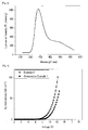
- the compounds (M-2 to M-4 and M-6 to M-9) of Examples 1 to 7 were measured regarding molecular weight to analyze the structure by using a liquid chromatography-mass analyzer (LC-MS, liquid chromatograph-mass spectrometry). LC-MS data of the compound M-6 prepared in Example 4 is shown in FIG. 2 .
- LC-MS liquid chromatography-mass analyzer
- FIG. 3 shows the PL wavelength result of the M-6 according to Example 4. Referring to FIG. 3 , when it was fabricated into a thin film, the M-6 had a maximum light emitting wavelength at 390 nm.
- Example 8 Devicefabrication using a solution process
- An ITO substrate was used as an anode.
- the anode was spin-coated to form poly(3,4-ethylenedioxy-thiophene) (PEDOT) on the top thereof.
- PEDOT poly(3,4-ethylenedioxy-thiophene)
- an emission layer 400 ⁇ was spin-coated on the surface of the PEDOT by doping M-6 of Example 4 as a host and about 13 wt% of Ir(mppy) 3 as a dopant.
- BAlq was vacuum-deposited to be 50 ⁇ thick to form a hole blocking layer.
- Alq 3 was vacuum-deposited to be 200 ⁇ thick on top of the emission layer to form an electron transport layer (ETL).
- ETL electron transport layer
- 10 ⁇ LiF and 1000 ⁇ Al were sequentially vacuum-deposited to fabricate a cathode.
- the anode and the cathode were used to fabricate an organic photoelectric device.
- the organic photoelectric device included a 5-layered organic thin layer, and in particular, it was ITO 1500 ⁇ / PEDOT 600 ⁇ / EML (M-6:Ir(mppy) 3 ) 400 ⁇ / BAlq 50 ⁇ / Alq 3 200 ⁇ / LiF 10 ⁇ / Al 1000 ⁇ .
- Comparative Example 1 Devicefabrication using a solution process
- a device included ITO 1500 ⁇ / PEDOT 600 ⁇ / EML (TCTA:TPBI 1:1, Ir(mppy) 3 ) 400 ⁇ / BAlq 50 ⁇ / Alq 3 200 ⁇ / LiF 10 ⁇ / Al 1000 ⁇ .
- the emission layer was spin-coated to be 400 ⁇ thick by doping a mixture of 4,4',4"-tris(N-carbazolyl)triphenylamine (TCTA) and 2,2',2"-(1,3,5-benzenetriyl)tris(1-phenyl-1H-benzimidazole) (TPBI) prepared in a weight ratio of 1:1 as a host and about 13 wt% of Ir(mppy) 3 as a dopant.
- TCTA 4,4',4"-tris(N-carbazolyl)triphenylamine
- TPBI 2,2',2"-(1,3,5-benzenetriyl)tris(1-phenyl-1H-benzimidazole)
- a device using a solution process was fabricated according to the same method as in Example 8, except for the above.
- Example 9 Devicefabrication using a deposition process
- An ITO substrate was used as an anode, and a device was fabricated by vacuum-depositing a layer thereon.
- the device of Example 9 included a hole transport layer (HTL) formed by vacuum-depositing 4,4'-bis[N-[4-(N,N-di-m-tolylamino)phenyl]-N-phenylamino]biphenyl (DNTPD) and N-(1-naphthyl)-N-phenyl-amino]biphenyl (NPB) to be respectively 600 ⁇ and 200 ⁇ thick.
- HTL hole transport layer
- BCP 2,9-dimethyl-4,7-diphenyl-1,10-phenanthroline
- the device using a deposit process was fabricated in the same method as in Example 8.
- a device including an emission layer was formed by vacuum-depositing 4,4'-N,N'-dicarbazole-bipheyl (CBP) as a host and 7 wt% of Ir(ppy) 3 as a dopant to be 300 ⁇ thick.
- CBP 4,4'-N,N'-dicarbazole-bipheyl
- the device using a deposition process device was fabricated according the same method as in Example 9 except for the above.
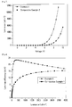
- the organic light emitting diodes according to Examples 8 to 9 and Comparative Examples 1 and 2 were measured regarding current density and luminance change depending on voltage change and luminous efficiency change depending on luminance change. Specifically, they were measured as follows.
- Each organic light emitting diode was measured regarding current value by using a current-voltage device (Keithley 2400) while its voltage was increased from 0. The current value was divided by area to calculate current density. The results are provided in FIGs. 4 and 5 .
- the organic light emitting diodes were measured regarding luminance by using a luminance meter (Minolta Cs-1000A) while its voltage was increased from 0. The results are provided in FIGs. 6 and 7 .
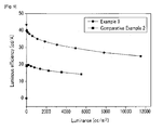
- the organic light emitting diodes were measured regarding luminous efficiency change depending on luminance change. The results are provided in FIGs. 8 and 9 .
- Tables 1 and 2 comprehensively show all the results.
- Table 1 shows performance evaluation results of the solution process devices according to Comparative Example 1 and Example 8.
- Emission layer material at 1000 cd/m 2 Threshold voltage V turn on Max. luminous efficiency Driving voltage Luminous efficiency (V) (cd/A) (Im/w) (V) (cd/A) (Im/W) Comp. Ex. 1 TCTA:TPBI (1:1) 9.80 13.90 4.45 4.80 16.50 4.71 Ex. 8 M-6 8.2 21.7 8.3 4.0 22.8 10.4
- a benzimidazole compound according to one embodiment of the present invention turned out to decrease the driving voltage of an organic light emitting diode as a host material and improve luminance and efficiency.
- Table 2 shows performance evaluation results of the deposition process devices according to Comparative Example 2 and Example 9.
- Table 2 Emission layer material at 1000 cd/m 2 Threshold voltage V turn on Max. luminous efficiency Driving voltage Luminous efficiency (V) (cd/A) (Im/w) (V) (cd/A) (Im/W) Comp. Ex. 2 CBP 8.8 17.8 7.6 5 19.7 11.3 Ex. 9 M-4 7.0 35.4 19.3 3.5 43.5 43.2
- a benzimidazole compound according to one embodiment of the present invention turned out to decrease the driving voltage of an organic light emitting diode as a host material and improve luminance and efficiency.
Landscapes
- Chemical & Material Sciences (AREA)
- Organic Chemistry (AREA)
- Engineering & Computer Science (AREA)
- Materials Engineering (AREA)
- Physics & Mathematics (AREA)
- Spectroscopy & Molecular Physics (AREA)
- Electroluminescent Light Sources (AREA)
- Plural Heterocyclic Compounds (AREA)
Applications Claiming Priority (2)
| Application Number | Priority Date | Filing Date | Title |
|---|---|---|---|
| KR20080100726 | 2008-10-14 | ||
| PCT/KR2009/005911 WO2010044607A1 (en) | 2008-10-14 | 2009-10-14 | Benzimidazole compounds and organic photoelectric device with the same |
Publications (3)
| Publication Number | Publication Date |
|---|---|
| EP2344611A1 EP2344611A1 (en) | 2011-07-20 |
| EP2344611A4 EP2344611A4 (en) | 2012-04-04 |
| EP2344611B1 true EP2344611B1 (en) | 2014-02-26 |
Family
ID=42106682
Family Applications (1)
| Application Number | Title | Priority Date | Filing Date |
|---|---|---|---|
| EP09820757.4A Active EP2344611B1 (en) | 2008-10-14 | 2009-10-14 | Benzimidazole compounds and organic photoelectric device with the same |
Country Status (7)
Families Citing this family (36)
| Publication number | Priority date | Publication date | Assignee | Title |
|---|---|---|---|---|
| CN102272262B (zh) | 2008-12-30 | 2014-09-10 | 第一毛织株式会社 | 有机光电装置用新化合物和包括该化合物的有机光电装置 |
| CN102596939B (zh) | 2009-09-16 | 2014-08-13 | 日东电工株式会社 | 用于有机发光二极管发射层的化合物 |
| JP5620125B2 (ja) * | 2010-01-28 | 2014-11-05 | ユー・ディー・シー アイルランド リミテッド | 有機電界発光素子 |
| TW201204811A (en) | 2010-07-19 | 2012-02-01 | Nitto Denko Corp | Phototherapy devices and methods comprising substituted carbazole compounds |
| JP5872861B2 (ja) * | 2010-11-30 | 2016-03-01 | 株式会社半導体エネルギー研究所 | カルバゾール化合物 |
| US8426040B2 (en) * | 2010-12-22 | 2013-04-23 | Nitto Denko Corporation | Compounds for use in light-emitting devices |
| WO2012103380A1 (en) * | 2011-01-27 | 2012-08-02 | Nitto Denko Corporation | Phototherapy devices and methods comprising optionally substituted terphenyl and quaterphenyl compounds |
| US8933243B2 (en) | 2011-06-22 | 2015-01-13 | Nitto Denko Corporation | Polyphenylene host compounds |
| KR101474797B1 (ko) | 2011-08-08 | 2014-12-19 | 제일모직 주식회사 | 유기광전자소자용 화합물 및 이를 포함하는 유기발광소자 |
| TWI465441B (zh) | 2011-08-12 | 2014-12-21 | Ind Tech Res Inst | 含乙烯官能基之咪唑衍生物及其用於電致發光元件之用途 |
| US9353085B2 (en) * | 2011-08-26 | 2016-05-31 | E-Ray Optoelectronics Technology Co., Ltd. | Compound for organic electroluminescent device and organic electroluminescent devices using the same |
| JP5839912B2 (ja) * | 2011-09-22 | 2016-01-06 | 株式会社半導体エネルギー研究所 | 発光素子、発光装置 |
| KR101474798B1 (ko) * | 2011-12-23 | 2014-12-22 | 제일모직 주식회사 | 유기광전자소자용 화합물, 이를 포함하는 유기발광소자 및 상기 유기발광소자를 포함하는 표시장치 |
| EP2836570A1 (en) * | 2012-04-13 | 2015-02-18 | Nitto Denko Corporation | Phototherapy devices and methods comprising optionally substitutted quinquiesphenyl compounds |
| US9966538B2 (en) | 2012-11-07 | 2018-05-08 | Lms Co., Ltd. | Compound, light-emitting element and electronic device comprising same |
| WO2014093353A1 (en) | 2012-12-10 | 2014-06-19 | Nitto Denko Corporation | Organic light emitting polyaromatic and polyheteroaromatic host materials |
| WO2014093361A1 (en) | 2012-12-10 | 2014-06-19 | Nitto Denko Corporation | Bipolar hosts for light emitting devices |
| TWI622497B (zh) | 2012-12-17 | 2018-05-01 | 日東電工股份有限公司 | 包含發光層之發光裝置 |
| KR101433822B1 (ko) * | 2013-06-17 | 2014-08-27 | 삼성디스플레이 주식회사 | 유기 발광 장치 |
| CN103539818B (zh) * | 2013-06-21 | 2016-11-09 | Tcl集团股份有限公司 | 双极性磷光主体化合物、制备方法和应用及电致发光器件 |
| JP6627508B2 (ja) * | 2013-08-14 | 2020-01-08 | コニカミノルタ株式会社 | 有機エレクトロルミネッセンス素子、照明装置、表示装置及び蛍光発光性化合物 |
| KR102162796B1 (ko) * | 2013-08-22 | 2020-10-08 | 삼성디스플레이 주식회사 | 유기 발광 소자 |
| JP2016136582A (ja) | 2015-01-23 | 2016-07-28 | 三星ディスプレイ株式會社Samsung Display Co.,Ltd. | 有機電界発光素子用材料、これを用いた有機電界発光素子及びアミン誘導体 |
| EP3307735A1 (en) | 2015-06-10 | 2018-04-18 | Merck Patent GmbH | Materials for organic electroluminescent devices |
| CN105294670B (zh) * | 2015-11-20 | 2019-07-09 | 上海天马有机发光显示技术有限公司 | 有机电致发光化合物及其有机光电装置 |
| CN108368088A (zh) * | 2015-12-08 | 2018-08-03 | 喜星素材株式会社 | 杂环化合物和使用其的有机发光器件 |
| KR102654859B1 (ko) | 2016-06-16 | 2024-04-05 | 삼성전자주식회사 | 축합환 화합물 및 이를 포함한 유기 발광 소자 |
| TWI589673B (zh) * | 2016-11-03 | 2017-07-01 | 元智大學 | 雙極性材料以及有機發光二極體元件 |
| KR102729197B1 (ko) * | 2017-02-08 | 2024-11-12 | 솔루스첨단소재 주식회사 | 유기 화합물 및 이를 이용한 유기 전계 발광 소자 |
| CN108503628A (zh) * | 2017-02-27 | 2018-09-07 | 上海和辉光电有限公司 | 一种有机电致发光化合物 |
| CN108440573B (zh) * | 2018-03-27 | 2022-05-20 | 武汉天马微电子有限公司 | 一种化合物及制备方法、一种有机发光显示装置 |
| CN108912148A (zh) * | 2018-08-12 | 2018-11-30 | 瑞声科技(南京)有限公司 | 一种含有氮杂咔唑-咪唑单元的化合物及其应用 |
| WO2020111601A1 (ko) * | 2018-11-27 | 2020-06-04 | 주식회사 엘지화학 | 신규한 화합물 및 이를 포함하는 유기발광 소자 |
| CN110483408A (zh) * | 2019-08-30 | 2019-11-22 | 陕西师范大学 | 一种大双折射率的n-甲基取代苯并咪唑侧氟液晶化合物及其制备方法 |
| CN110483409A (zh) * | 2019-09-04 | 2019-11-22 | 陕西师范大学 | N-甲基取代苯并咪唑类含氟液晶化合物及其制备方法 |
| CN111171010A (zh) * | 2020-01-13 | 2020-05-19 | 北京大学深圳研究生院 | 一种阴极电刺激响应材料及其制备方法 |
Family Cites Families (36)
| Publication number | Priority date | Publication date | Assignee | Title |
|---|---|---|---|---|
| JPS5975257A (ja) * | 1982-10-23 | 1984-04-27 | Ricoh Co Ltd | 電子写真用感光体 |
| US5766779A (en) * | 1996-08-20 | 1998-06-16 | Eastman Kodak Company | Electron transporting materials for organic electroluminescent devices |
| JP4105358B2 (ja) * | 2000-03-07 | 2008-06-25 | 富士フイルム株式会社 | ベンズイミダゾール誘導体、発光素子材料及び発光素子 |
| JP4951829B2 (ja) * | 2000-09-25 | 2012-06-13 | コニカミノルタホールディングス株式会社 | 有機エレクトロルミネッセンス素子および表示装置 |
| US6998487B2 (en) | 2001-04-27 | 2006-02-14 | Lg Chem, Ltd. | Double-spiro organic compounds and organic electroluminescent devices using the same |
| AU2002354442A1 (en) * | 2001-12-12 | 2003-06-23 | Tokuyama Corporation | Organic electroluminescent materials |
| JP2003313546A (ja) * | 2002-04-24 | 2003-11-06 | Tokuyama Corp | 発光性組成物 |
| JP4401665B2 (ja) * | 2003-03-20 | 2010-01-20 | 株式会社半導体エネルギー研究所 | 電界発光素子 |
| JP2004292766A (ja) * | 2003-03-28 | 2004-10-21 | Tokuyama Corp | 有機エレクトロルミネッセンス素子材料 |
| JP2004352655A (ja) * | 2003-05-29 | 2004-12-16 | Idemitsu Kosan Co Ltd | スピロ結合含有化合物及びそれを用いた有機エレクトロルミネッセンス素子 |
| US20050065094A1 (en) * | 2003-09-05 | 2005-03-24 | Boehringer Ingelheim International Gmbh | Use of telmisartan for the prevention and treatment of vascular headache |
| JP4682503B2 (ja) * | 2003-09-16 | 2011-05-11 | 東洋インキ製造株式会社 | 有機エレクトロルミネッセンス素子用材料およびそれを用いた有機エレクトロルミネッセンス素子 |
| TWI428053B (zh) * | 2004-02-09 | 2014-02-21 | Idemitsu Kosan Co | Organic electroluminescent element |
| US7288329B2 (en) * | 2004-02-25 | 2007-10-30 | Eastman Kodak Company | Electroluminescent devices including conjugated polymers containing an azole structure |
| TWI306449B (en) * | 2004-09-24 | 2009-02-21 | Lg Chemical Ltd | New compound and organic light emitting device using the same (1) |
| JP2007039406A (ja) * | 2005-08-05 | 2007-02-15 | Idemitsu Kosan Co Ltd | 含窒素複素環誘導体及びそれを用いた有機エレクトロルミネッセンス素子 |
| JP4991737B2 (ja) * | 2005-10-21 | 2012-08-01 | エルジー・ケム・リミテッド | 新規のビナフタレン誘導体、その製造方法およびそれを用いた有機電子素子 |
| US8053762B2 (en) * | 2005-12-13 | 2011-11-08 | Lg Chem, Ltd. | Imidazoquinazoline derivative, process for preparing the same, and organic electronic device using the same |
| KR100872692B1 (ko) * | 2006-03-06 | 2008-12-10 | 주식회사 엘지화학 | 신규한 안트라센 유도체 및 이를 이용한 유기 전자 소자 |
| JP4961540B2 (ja) * | 2006-03-09 | 2012-06-27 | 国立大学法人東京工業大学 | 有機エレクトロルミネッセンス素子用化合物、組成物および有機エレクトロルミネッセンス素子 |
| JPWO2007111262A1 (ja) * | 2006-03-27 | 2009-08-13 | 出光興産株式会社 | 含窒素複素環誘導体及びそれを用いた有機エレクトロルミネッセンス素子 |
| JP5003002B2 (ja) * | 2006-04-03 | 2012-08-15 | Jsr株式会社 | 有機エレクトロルミネッセンス素子用材料およびその製造方法、並びに有機エレクトロルミネッセンス素子 |
| KR101321500B1 (ko) * | 2006-09-29 | 2013-10-30 | 삼성디스플레이 주식회사 | 유기 전계 발광 화합물 및 이를 이용한 유기 전계 발광소자 |
| KR101328974B1 (ko) | 2006-10-31 | 2013-11-13 | 삼성디스플레이 주식회사 | 유기 전계 발광 화합물 및 이를 이용한 유기 전계 발광소자 |
| KR100989467B1 (ko) | 2006-12-06 | 2010-10-22 | 주식회사 엘지화학 | 신규한 플루오렌 유도체 및 이를 이용한 유기 전자 소자 |
| TWI373987B (en) * | 2007-03-07 | 2012-10-01 | Sony Corp | Organic electroluminescent device and display device |
| US20080278072A1 (en) * | 2007-04-30 | 2008-11-13 | Lg Chem, Ltd. | Organic light emitting device and method of producing the same |
| TWI394746B (zh) * | 2007-11-16 | 2013-05-01 | Academia Sinica | 有機電激發光裝置及其材料 |
| JP5317470B2 (ja) * | 2007-12-27 | 2013-10-16 | 出光興産株式会社 | 有機エレクトロルミネッセンス素子用材料及びそれを用いた有機エレクトロルミネッセンス素子 |
| WO2009084544A1 (ja) * | 2007-12-27 | 2009-07-09 | Idemitsu Kosan Co., Ltd. | 含窒素複素環誘導体及びそれを用いた有機エレクトロルミネッセンス素子 |
| KR100959189B1 (ko) * | 2007-12-31 | 2010-05-24 | 제일모직주식회사 | 저분자 유기화합물, 및 이를 포함하는 유기광전소자 |
| KR100952966B1 (ko) * | 2007-12-31 | 2010-04-15 | 제일모직주식회사 | 유기광전소자용 유기금속착체 화합물, 및 이를 포함하는유기광전소자 |
| KR100901887B1 (ko) * | 2008-03-14 | 2009-06-09 | (주)그라쎌 | 신규한 유기 발광 화합물 및 이를 채용하고 있는 유기 발광소자 |
| KR100910150B1 (ko) | 2008-04-02 | 2009-08-03 | (주)그라쎌 | 신규한 유기 발광 화합물 및 이를 발광재료로서 채용하고있는 유기 발광 소자 |
| CN102272262B (zh) * | 2008-12-30 | 2014-09-10 | 第一毛织株式会社 | 有机光电装置用新化合物和包括该化合物的有机光电装置 |
| JP5839912B2 (ja) * | 2011-09-22 | 2016-01-06 | 株式会社半導体エネルギー研究所 | 発光素子、発光装置 |
-
2009
- 2009-10-14 EP EP09820757.4A patent/EP2344611B1/en active Active
- 2009-10-14 KR KR1020090097762A patent/KR101333697B1/ko active Active
- 2009-10-14 TW TW098134766A patent/TWI530493B/zh active
- 2009-10-14 CN CN2009801363654A patent/CN102159668A/zh active Pending
- 2009-10-14 WO PCT/KR2009/005911 patent/WO2010044607A1/en active Application Filing
- 2009-10-14 JP JP2011530963A patent/JP5694939B2/ja active Active
-
2011
- 2011-04-14 US US13/086,640 patent/US20110272676A1/en not_active Abandoned
-
2013
- 2013-05-13 US US13/892,604 patent/US9530970B2/en active Active
Also Published As
| Publication number | Publication date |
|---|---|
| US20110272676A1 (en) | 2011-11-10 |
| TW201022232A (en) | 2010-06-16 |
| EP2344611A1 (en) | 2011-07-20 |
| KR20100041690A (ko) | 2010-04-22 |
| US9530970B2 (en) | 2016-12-27 |
| EP2344611A4 (en) | 2012-04-04 |
| KR101333697B1 (ko) | 2013-11-27 |
| TWI530493B (zh) | 2016-04-21 |
| JP2012505829A (ja) | 2012-03-08 |
| JP5694939B2 (ja) | 2015-04-01 |
| WO2010044607A1 (en) | 2010-04-22 |
| CN102159668A (zh) | 2011-08-17 |
| US20130256641A1 (en) | 2013-10-03 |
Similar Documents
| Publication | Publication Date | Title |
|---|---|---|
| EP2344611B1 (en) | Benzimidazole compounds and organic photoelectric device with the same | |
| KR100959189B1 (ko) | 저분자 유기화합물, 및 이를 포함하는 유기광전소자 | |
| KR101311934B1 (ko) | 유기광전소자용 조성물 및 이를 이용한 유기광전소자 | |
| KR101002733B1 (ko) | 유기 화합물, 및 이를 포함하는 유기광전소자 | |
| KR101247626B1 (ko) | 유기광전소자용 화합물 및 이를 포함하는 유기광전소자 | |
| EP2452997A2 (en) | Compound for an organic photoelectric element, and an organic photoelectric element comprising the same | |
| KR101474801B1 (ko) | 유기광전자소자용 화합물, 이를 포함하는 유기발광소자 및 상기 유기발광소자를 포함하는 표시장치 | |
| US8603646B2 (en) | Pyrrole compound and organic photoelectric device including the same | |
| US20120091446A1 (en) | Compound for optoelectronic device, organic light emitting diode including the same and display including the organic light emitting diode | |
| EP2207834B1 (en) | Polymer, and organic photoelectric device comprising the same | |
| KR101474797B1 (ko) | 유기광전자소자용 화합물 및 이를 포함하는 유기발광소자 | |
| EP3006433B1 (en) | Compound, organic light emitting element comprising same, and display device comprising organic light emitting element | |
| JP2003012777A (ja) | 白色電界発光高分子化合物およびこれを用いた有機電界発光素子 | |
| KR101474800B1 (ko) | 유기광전자소자용 화합물, 이를 포함하는 유기발광소자 및 상기 유기발광소자를 포함하는 표시장치 | |
| KR20090028346A (ko) | 유기 화합물, 및 이를 포함하는 유기광전소자 | |
| KR20200072891A (ko) | 지연형광 화합물, 이를 포함하는 유기발광다이오드 및 유기발광표시장치 | |
| EP3680261A1 (en) | Polymer, coating composition comprising same, and organic light emitting element using same | |
| KR101507000B1 (ko) | 유기광전자소자용 화합물, 이를 포함하는 유기발광소자 및 상기 유기발광소자를 포함하는 표시장치 | |
| KR20050095613A (ko) | 발광소자, 그것에 이용하는 축합다환계 화합물 및 그제조방법 | |
| EP2998380A1 (en) | Compound for organic optoelectric device, organic light-emitting diode including same, display device including organic light-emitting diode | |
| KR100951707B1 (ko) | 사이클로헥산을 포함하는 유기광전소자용 재료 및 이를포함하는 유기광전소자 | |
| KR20130117534A (ko) | 유기광전자소자용 화합물, 이를 포함하는 유기발광소자 및 상기 유기발광소자를 포함하는 표시장치 | |
| TW202246278A (zh) | 化合物、發光材料及有機發光元件 | |
| KR102519548B1 (ko) | 유기 화합물과 이를 포함하는 유기발광다이오드 및 유기발광 표시장치 | |
| KR20090068193A (ko) | 유기 화합물, 및 이를 포함하는 유기광전소자 |
Legal Events
| Date | Code | Title | Description |
|---|---|---|---|
| PUAI | Public reference made under article 153(3) epc to a published international application that has entered the european phase |
Free format text: ORIGINAL CODE: 0009012 |
|
| 17P | Request for examination filed |
Effective date: 20110503 |
|
| AK | Designated contracting states |
Kind code of ref document: A1 Designated state(s): AT BE BG CH CY CZ DE DK EE ES FI FR GB GR HR HU IE IS IT LI LT LU LV MC MK MT NL NO PL PT RO SE SI SK SM TR |
|
| AX | Request for extension of the european patent |
Extension state: AL BA RS |
|
| DAX | Request for extension of the european patent (deleted) | ||
| A4 | Supplementary search report drawn up and despatched |
Effective date: 20120306 |
|
| RIC1 | Information provided on ipc code assigned before grant |
Ipc: C09K 19/32 20060101ALI20120229BHEP Ipc: C09K 19/34 20060101ALI20120229BHEP Ipc: C09K 19/04 20060101AFI20120229BHEP |
|
| 17Q | First examination report despatched |
Effective date: 20121214 |
|
| GRAP | Despatch of communication of intention to grant a patent |
Free format text: ORIGINAL CODE: EPIDOSNIGR1 |
|
| INTG | Intention to grant announced |
Effective date: 20130925 |
|
| GRAS | Grant fee paid |
Free format text: ORIGINAL CODE: EPIDOSNIGR3 |
|
| GRAA | (expected) grant |
Free format text: ORIGINAL CODE: 0009210 |
|
| AK | Designated contracting states |
Kind code of ref document: B1 Designated state(s): AT BE BG CH CY CZ DE DK EE ES FI FR GB GR HR HU IE IS IT LI LT LU LV MC MK MT NL NO PL PT RO SE SI SK SM TR |
|
| REG | Reference to a national code |
Ref country code: GB Ref legal event code: FG4D |
|
| REG | Reference to a national code |
Ref country code: CH Ref legal event code: EP |
|
| REG | Reference to a national code |
Ref country code: AT Ref legal event code: REF Ref document number: 653617 Country of ref document: AT Kind code of ref document: T Effective date: 20140315 |
|
| REG | Reference to a national code |
Ref country code: IE Ref legal event code: FG4D |
|
| REG | Reference to a national code |
Ref country code: DE Ref legal event code: R096 Ref document number: 602009022093 Country of ref document: DE Effective date: 20140410 |
|
| REG | Reference to a national code |
Ref country code: NL Ref legal event code: VDEP Effective date: 20140226 |
|
| REG | Reference to a national code |
Ref country code: AT Ref legal event code: MK05 Ref document number: 653617 Country of ref document: AT Kind code of ref document: T Effective date: 20140226 |
|
| REG | Reference to a national code |
Ref country code: LT Ref legal event code: MG4D |
|
| PG25 | Lapsed in a contracting state [announced via postgrant information from national office to epo] |
Ref country code: NO Free format text: LAPSE BECAUSE OF FAILURE TO SUBMIT A TRANSLATION OF THE DESCRIPTION OR TO PAY THE FEE WITHIN THE PRESCRIBED TIME-LIMIT Effective date: 20140526 Ref country code: IS Free format text: LAPSE BECAUSE OF FAILURE TO SUBMIT A TRANSLATION OF THE DESCRIPTION OR TO PAY THE FEE WITHIN THE PRESCRIBED TIME-LIMIT Effective date: 20140626 Ref country code: LT Free format text: LAPSE BECAUSE OF FAILURE TO SUBMIT A TRANSLATION OF THE DESCRIPTION OR TO PAY THE FEE WITHIN THE PRESCRIBED TIME-LIMIT Effective date: 20140226 |
|
| PG25 | Lapsed in a contracting state [announced via postgrant information from national office to epo] |
Ref country code: SE Free format text: LAPSE BECAUSE OF FAILURE TO SUBMIT A TRANSLATION OF THE DESCRIPTION OR TO PAY THE FEE WITHIN THE PRESCRIBED TIME-LIMIT Effective date: 20140226 Ref country code: NL Free format text: LAPSE BECAUSE OF FAILURE TO SUBMIT A TRANSLATION OF THE DESCRIPTION OR TO PAY THE FEE WITHIN THE PRESCRIBED TIME-LIMIT Effective date: 20140226 Ref country code: AT Free format text: LAPSE BECAUSE OF FAILURE TO SUBMIT A TRANSLATION OF THE DESCRIPTION OR TO PAY THE FEE WITHIN THE PRESCRIBED TIME-LIMIT Effective date: 20140226 Ref country code: FI Free format text: LAPSE BECAUSE OF FAILURE TO SUBMIT A TRANSLATION OF THE DESCRIPTION OR TO PAY THE FEE WITHIN THE PRESCRIBED TIME-LIMIT Effective date: 20140226 Ref country code: PT Free format text: LAPSE BECAUSE OF FAILURE TO SUBMIT A TRANSLATION OF THE DESCRIPTION OR TO PAY THE FEE WITHIN THE PRESCRIBED TIME-LIMIT Effective date: 20140626 Ref country code: CY Free format text: LAPSE BECAUSE OF FAILURE TO SUBMIT A TRANSLATION OF THE DESCRIPTION OR TO PAY THE FEE WITHIN THE PRESCRIBED TIME-LIMIT Effective date: 20140226 |
|
| PG25 | Lapsed in a contracting state [announced via postgrant information from national office to epo] |
Ref country code: BE Free format text: LAPSE BECAUSE OF FAILURE TO SUBMIT A TRANSLATION OF THE DESCRIPTION OR TO PAY THE FEE WITHIN THE PRESCRIBED TIME-LIMIT Effective date: 20140226 Ref country code: LV Free format text: LAPSE BECAUSE OF FAILURE TO SUBMIT A TRANSLATION OF THE DESCRIPTION OR TO PAY THE FEE WITHIN THE PRESCRIBED TIME-LIMIT Effective date: 20140226 Ref country code: HR Free format text: LAPSE BECAUSE OF FAILURE TO SUBMIT A TRANSLATION OF THE DESCRIPTION OR TO PAY THE FEE WITHIN THE PRESCRIBED TIME-LIMIT Effective date: 20140226 |
|
| PG25 | Lapsed in a contracting state [announced via postgrant information from national office to epo] |
Ref country code: EE Free format text: LAPSE BECAUSE OF FAILURE TO SUBMIT A TRANSLATION OF THE DESCRIPTION OR TO PAY THE FEE WITHIN THE PRESCRIBED TIME-LIMIT Effective date: 20140226 Ref country code: RO Free format text: LAPSE BECAUSE OF FAILURE TO SUBMIT A TRANSLATION OF THE DESCRIPTION OR TO PAY THE FEE WITHIN THE PRESCRIBED TIME-LIMIT Effective date: 20140226 Ref country code: DK Free format text: LAPSE BECAUSE OF FAILURE TO SUBMIT A TRANSLATION OF THE DESCRIPTION OR TO PAY THE FEE WITHIN THE PRESCRIBED TIME-LIMIT Effective date: 20140226 Ref country code: CZ Free format text: LAPSE BECAUSE OF FAILURE TO SUBMIT A TRANSLATION OF THE DESCRIPTION OR TO PAY THE FEE WITHIN THE PRESCRIBED TIME-LIMIT Effective date: 20140226 |
|
| REG | Reference to a national code |
Ref country code: DE Ref legal event code: R097 Ref document number: 602009022093 Country of ref document: DE |
|
| PG25 | Lapsed in a contracting state [announced via postgrant information from national office to epo] |
Ref country code: SK Free format text: LAPSE BECAUSE OF FAILURE TO SUBMIT A TRANSLATION OF THE DESCRIPTION OR TO PAY THE FEE WITHIN THE PRESCRIBED TIME-LIMIT Effective date: 20140226 Ref country code: PL Free format text: LAPSE BECAUSE OF FAILURE TO SUBMIT A TRANSLATION OF THE DESCRIPTION OR TO PAY THE FEE WITHIN THE PRESCRIBED TIME-LIMIT Effective date: 20140226 Ref country code: ES Free format text: LAPSE BECAUSE OF FAILURE TO SUBMIT A TRANSLATION OF THE DESCRIPTION OR TO PAY THE FEE WITHIN THE PRESCRIBED TIME-LIMIT Effective date: 20140226 |
|
| PLBE | No opposition filed within time limit |
Free format text: ORIGINAL CODE: 0009261 |
|
| STAA | Information on the status of an ep patent application or granted ep patent |
Free format text: STATUS: NO OPPOSITION FILED WITHIN TIME LIMIT |
|
| 26N | No opposition filed |
Effective date: 20141127 |
|
| REG | Reference to a national code |
Ref country code: DE Ref legal event code: R097 Ref document number: 602009022093 Country of ref document: DE Effective date: 20141127 |
|
| PG25 | Lapsed in a contracting state [announced via postgrant information from national office to epo] |
Ref country code: IT Free format text: LAPSE BECAUSE OF FAILURE TO SUBMIT A TRANSLATION OF THE DESCRIPTION OR TO PAY THE FEE WITHIN THE PRESCRIBED TIME-LIMIT Effective date: 20140226 |
|
| PG25 | Lapsed in a contracting state [announced via postgrant information from national office to epo] |
Ref country code: MC Free format text: LAPSE BECAUSE OF FAILURE TO SUBMIT A TRANSLATION OF THE DESCRIPTION OR TO PAY THE FEE WITHIN THE PRESCRIBED TIME-LIMIT Effective date: 20140226 Ref country code: LU Free format text: LAPSE BECAUSE OF FAILURE TO SUBMIT A TRANSLATION OF THE DESCRIPTION OR TO PAY THE FEE WITHIN THE PRESCRIBED TIME-LIMIT Effective date: 20141014 |
|
| REG | Reference to a national code |
Ref country code: CH Ref legal event code: PL |
|
| GBPC | Gb: european patent ceased through non-payment of renewal fee |
Effective date: 20141014 |
|
| REG | Reference to a national code |
Ref country code: IE Ref legal event code: MM4A |
|
| PG25 | Lapsed in a contracting state [announced via postgrant information from national office to epo] |
Ref country code: LI Free format text: LAPSE BECAUSE OF NON-PAYMENT OF DUE FEES Effective date: 20141031 Ref country code: GB Free format text: LAPSE BECAUSE OF NON-PAYMENT OF DUE FEES Effective date: 20141014 Ref country code: CH Free format text: LAPSE BECAUSE OF NON-PAYMENT OF DUE FEES Effective date: 20141031 |
|
| REG | Reference to a national code |
Ref country code: FR Ref legal event code: ST Effective date: 20150630 |
|
| PG25 | Lapsed in a contracting state [announced via postgrant information from national office to epo] |
Ref country code: FR Free format text: LAPSE BECAUSE OF NON-PAYMENT OF DUE FEES Effective date: 20141031 |
|
| PG25 | Lapsed in a contracting state [announced via postgrant information from national office to epo] |
Ref country code: IE Free format text: LAPSE BECAUSE OF NON-PAYMENT OF DUE FEES Effective date: 20141014 |
|
| PG25 | Lapsed in a contracting state [announced via postgrant information from national office to epo] |
Ref country code: SM Free format text: LAPSE BECAUSE OF FAILURE TO SUBMIT A TRANSLATION OF THE DESCRIPTION OR TO PAY THE FEE WITHIN THE PRESCRIBED TIME-LIMIT Effective date: 20140226 |
|
| PG25 | Lapsed in a contracting state [announced via postgrant information from national office to epo] |
Ref country code: GR Free format text: LAPSE BECAUSE OF FAILURE TO SUBMIT A TRANSLATION OF THE DESCRIPTION OR TO PAY THE FEE WITHIN THE PRESCRIBED TIME-LIMIT Effective date: 20140527 Ref country code: BG Free format text: LAPSE BECAUSE OF FAILURE TO SUBMIT A TRANSLATION OF THE DESCRIPTION OR TO PAY THE FEE WITHIN THE PRESCRIBED TIME-LIMIT Effective date: 20140226 |
|
| PG25 | Lapsed in a contracting state [announced via postgrant information from national office to epo] |
Ref country code: TR Free format text: LAPSE BECAUSE OF FAILURE TO SUBMIT A TRANSLATION OF THE DESCRIPTION OR TO PAY THE FEE WITHIN THE PRESCRIBED TIME-LIMIT Effective date: 20140226 Ref country code: MT Free format text: LAPSE BECAUSE OF FAILURE TO SUBMIT A TRANSLATION OF THE DESCRIPTION OR TO PAY THE FEE WITHIN THE PRESCRIBED TIME-LIMIT Effective date: 20140226 Ref country code: SI Free format text: LAPSE BECAUSE OF FAILURE TO SUBMIT A TRANSLATION OF THE DESCRIPTION OR TO PAY THE FEE WITHIN THE PRESCRIBED TIME-LIMIT Effective date: 20140226 Ref country code: HU Free format text: LAPSE BECAUSE OF FAILURE TO SUBMIT A TRANSLATION OF THE DESCRIPTION OR TO PAY THE FEE WITHIN THE PRESCRIBED TIME-LIMIT; INVALID AB INITIO Effective date: 20091014 |
|
| PG25 | Lapsed in a contracting state [announced via postgrant information from national office to epo] |
Ref country code: MK Free format text: LAPSE BECAUSE OF FAILURE TO SUBMIT A TRANSLATION OF THE DESCRIPTION OR TO PAY THE FEE WITHIN THE PRESCRIBED TIME-LIMIT Effective date: 20140226 |
|
| P01 | Opt-out of the competence of the unified patent court (upc) registered |
Effective date: 20230528 |
|
| PGFP | Annual fee paid to national office [announced via postgrant information from national office to epo] |
Ref country code: DE Payment date: 20240910 Year of fee payment: 16 |