EP2334055B1 - Dispositif de conversion photoélectrique - Google Patents
Dispositif de conversion photoélectrique Download PDFInfo
- Publication number
- EP2334055B1 EP2334055B1 EP10191141.0A EP10191141A EP2334055B1 EP 2334055 B1 EP2334055 B1 EP 2334055B1 EP 10191141 A EP10191141 A EP 10191141A EP 2334055 B1 EP2334055 B1 EP 2334055B1
- Authority
- EP
- European Patent Office
- Prior art keywords
- sensor
- signal
- noise
- cell
- transfer
- Prior art date
- Legal status (The legal status is an assumption and is not a legal conclusion. Google has not performed a legal analysis and makes no representation as to the accuracy of the status listed.)
- Not-in-force
Links
Images


Classifications
-
- H—ELECTRICITY
- H04—ELECTRIC COMMUNICATION TECHNIQUE
- H04N—PICTORIAL COMMUNICATION, e.g. TELEVISION
- H04N25/00—Circuitry of solid-state image sensors [SSIS]; Control thereof
- H04N25/60—Noise processing, e.g. detecting, correcting, reducing or removing noise
- H04N25/65—Noise processing, e.g. detecting, correcting, reducing or removing noise applied to reset noise, e.g. KTC noise related to CMOS structures by techniques other than CDS
-
- H—ELECTRICITY
- H04—ELECTRIC COMMUNICATION TECHNIQUE
- H04N—PICTORIAL COMMUNICATION, e.g. TELEVISION
- H04N23/00—Cameras or camera modules comprising electronic image sensors; Control thereof
- H04N23/60—Control of cameras or camera modules
- H04N23/67—Focus control based on electronic image sensor signals
- H04N23/672—Focus control based on electronic image sensor signals based on the phase difference signals
-
- H—ELECTRICITY
- H04—ELECTRIC COMMUNICATION TECHNIQUE
- H04N—PICTORIAL COMMUNICATION, e.g. TELEVISION
- H04N25/00—Circuitry of solid-state image sensors [SSIS]; Control thereof
- H04N25/70—SSIS architectures; Circuits associated therewith
- H04N25/76—Addressed sensors, e.g. MOS or CMOS sensors
- H04N25/77—Pixel circuitry, e.g. memories, A/D converters, pixel amplifiers, shared circuits or shared components
Definitions
- the present invention relates to a photoelectric-conversion device and particularly relates to a photoelectric-conversion device.
- an auto focusing (AF) sensor for detecting a focal point is provided in image pickup systems.
- the AF sensors have been expected to be capable of detecting a focal point with higher speed and higher precision.
- a solid-state image pickup device including a transfer system provided to transfer a signal which is output from a sensor-cell unit to a memory-cell unit has been disclosed in Japanese Patent Laid-Open No. 09-200614 . According to Japanese Patent Laid-Open No. 09-200614 , a plurality of the memory-cell units may be provided.
- a focus-detection device including a frame memory provided to store the accumulation signal corresponding to each of regions that are obtained by dividing a line sensor into at least two regions and a frame memory provided to store the accumulation signal corresponding to all of the regions of the line sensor has been disclosed in Japanese Patent Laid-Open No. 2006-220684 .
- the focal-point detection can be performed with high speed even in a case of a large amount of defocus.
- the document EP 1 549 050 A2 discloses an imaging apparatus for processing a noise signal and a photoelectric conversion signal.
- the imaging apparatus includes a pixel unit having a photoelectric conversion section and an amplifying device for amplifying a signal from the photoelectric conversion section and outputting the signal; a reading unit having a first mode in which a signal obtained by resetting an input section of the amplifying device is sampled a plurality of times via the amplifying device and a second mode in which a photoelectric conversion signal generated in the photoelectric conversion section is sampled a plurality of times via the amplifying device; a mixing unit for generating a first mixing signal by mixing the signals that are sampled in the first mode, outputting the first mixing signal, generating a second mixing signal by mixing the signals that are sampled in the second mode, and outputting the second mixing signal; and a difference processing unit for performing difference processing between the first mixing signal and the second mixing signal.
- the (post-published) document EP 2 343 880 A2 discloses a photoelectric-conversion device that allows for both of widening the dynamic range and performing an operation to monitor the amount of received light is achieved.
- a sensor-cell unit that can operate in low-sensitivity mode and high-sensitivity mode, a transfer unit transferring a signal output from a unit pixel, and a monitoring unit monitoring a signal transmitted from the sensor-cell unit, the signal being output from the transfer unit, are provided.
- the present invention has its object to provide a preferred configuration of a photoelectric-conversion device including a plurality of memory-cell units provided for a single sensor-cell unit.
- the present invention in its first aspect provides a device as specified in claims 1 to 5.
- the present invention in its second aspect provides a phase-difference detection-type focus-detection device as specified in claim 6.
- the present invention in its third aspect provides an image pickup system as specified in claim 7.
- the present invention allows for performing an appropriate operation through a photoelectric-conversion device including a plurality of memory-cell units provided for a single sensor-cell unit.
- the exemplary configuration involves providing two memory-cell units for a single sensor-cell unit, as is the case with Japanese Patent Laid-Open No. 2006-220684 , in a configuration disclosed in Japanese Patent Laid-Open No. 09-200614 .
- an operation is performed to write a noise signal of the sensor-cell unit into the memory-cell unit before performing an accumulation operation. Therefore, when the two memory-cell units are provided in the configuration disclosed in Japanese Patent Laid-Open No. 09-200614 , the noise-signal writing operation should be performed twice. That is, the noise signal should be written into the sensor-cell unit twice. Consequently, the timing when automatic gain control (hereinafter referred to as the AGC) is started after performing the noise-signal writing operation may be delayed.
- the AGC automatic gain control
- a problem may occur in case of an incident light with high intensity.
- the incident light with high intensity causes the sensor-cell unit to reach a signal-saturation level in a short time period. Therefore, when the AGC-start time is delayed, a signal may reach the saturation level before the AGC is started and the AGC may not be performed appropriately.
- the first embodiment shows an exemplary configuration where a photoelectric-conversion device is provided to perform the phase-difference focus detection (auto focusing (AF)).
- AF auto focusing
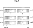
- Fig. 1 schematically illustrates an imaging area provided in the phase-difference AF photoelectric-conversion device. Pairs of line-sensor units L1A and L1B, L2A and L2B, ..., and LNA and LNB are provided on the imaging area. A pair of the line-sensor units is used to measure the defocusing amount of an object image, which is observed in a given region of the imaging area. Plural pairs of the line-sensor units are arranged to provide plural range-finding points and increase the AF precision. Each of the line-sensor units includes unit pixels 11A, 12A, and so forth.
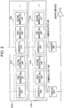
- Fig. 2 is a block diagram illustrating a part relating to the line-sensor units L1A, L2A, and so forth in more detail.
- Each of unit pixels includes a sensor-cell unit, a first memory-cell unit, and a second memory-cell unit, and is connected to a common-output line. Further, unit pixels of line-sensor units that are provided at positions equivalent to one another are connected to a common transfer unit via the common-output line. Each of the transfer units is connected to a common buffer amplifier.
- the configuration of each of the line-sensor units L1B, L2B, and so forth is the same as that illustrated in Fig. 2 .
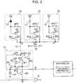
- Fig. 3 illustrates the line-sensor unit LS1 extracted from the configuration illustrated in Fig. 2 , and particularly illustrates the unit pixel 11A and a transfer unit connected thereto.
- the unit pixel 11A includes a sensor-cell unit 100, a first memory-cell unit 101, and a second memory-cell unit 102.
- the sign " ⁇ X" used to express each of the control electrodes and the switches of MOS transistors denotes a signal transmitted from a control unit (not shown).
- the sensor-cell unit 100 includes a photodiode (PD) 103 which is a photoelectric-conversion unit, a sensor-cell-unit writing switch 106, and metal-oxide-semiconductor (MOS) transistors M11 and M12.
- the anode of the PD 103 is connected to one of terminals of the sensor-cell-unit writing switch 106 and the control electrode of the MOS transistor M11, and the cathode of the PD 103 is connected to a power voltage VDD.
- MOS transistor M12 When the MOS transistor M12 is brought into conduction, the MOS transistors M11 and M12, and a load MOS transistor M13 form an inverting amplifier with a gain of -1.
- the sensor-cell unit 100 outputs an accumulation signal generated based on the amount of electrical charges that are obtained through the photoelectric conversion performed by the PD 103 to a common-output line 112 via the inverting amplifier. That is, the MOS transistor M12 functions as a selection switch used to select the sensor-cell unit 100.
- the sensor-cell-unit writing switch 106 is provided to switch between conduction and non-conduction states between the anode of the PD 103 and the common-output line 112.
- the sensor-cell-unit writing switch 106 may include a p-channel metal-oxide semiconductor (PMOS) transistor, an n-channel metal-oxide semiconductor (NMOS) transistor, a complementary metal-oxide semiconductor (CMOS) transistor, and so forth.
- each of the memory-cell units 101 and 102 is equivalent to that of the sensor-cell unit 100 except that the PD 103 provided in the sensor-cell unit 100 is replaced with each of the memory capacitances 104 and 105. Therefore, descriptions of each of the memory-cell units 101 and 102 will be omitted.
- the load-MOS transistor M13 is shared among the sensor-cell unit 100, and the memory-cell units 101 and 102. However, a single load-MOS transistor may be provided for each of the cell units.
- the transfer unit 113 includes MOS transistors M21, M22, M23, and M24, a transfer capacitance 117, a feedback switch 120, and a transfer switch 121.
- One of terminals of the transfer switch 121 is connected to the common-output line 112 and one of terminals of the feedback switch 120.
- the other terminal of the transfer switch 121 is connected to one of terminals of the transfer capacitance 117 and one of main electrodes of each of the MOS transistors M22 and M24.
- the other main electrode of the MOS transistor M22 is connected to a power voltage VRS.
- the other main electrode of the MOS transistor M24 which is an optical-signal reading switch, is connected to a buffer amplifier 123.
- the other terminal of the transfer capacitance 117 is connected to the control electrode of the MOS transistor M21 and one of main electrodes of the MOS transistor M23.
- One of main electrodes of the MOS transistor M21 is connected to a power voltage VDD and the other main electrode of the MOS transistor M21 is connected to a constant-current source 124, a node N6, and the other terminal of the feedback switch 120.
- the transfer unit 113 performs processing for the difference between a signal output from the sensor-cell unit 100, and a reset noise written into each of the memory-cell units 101 and 102, and a noise generated in the transfer unit 113 by performing operations which will be described later.
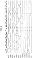
- Fig. 4 illustrates signals that are provided to the switches and/or the control electrodes of the MOS transistors that are illustrated in Fig. 3 .
- the sign "/" is used to express a signal provided to the PMOS transistor as an inverted signal. Therefore, the switches and the MOS transistors are brought into conduction when the signals corresponding to the switches and the MOS transistors, the signals being illustrated in Fig. 4 , go to high-level.
- each of signals ⁇ RS, ⁇ FT, ⁇ PS1, ⁇ PS2_1, ⁇ PS2_2, and ⁇ GR goes to high-level causing the sensor-cell-unit writing switch 106, the memory-cell unit writing switches 107 and 108, the transfer switch 121, and the MOS transistors M22 and M23 to be conductive. Accordingly, each of the PD 103, and the memory capacitances 104 and 105 is reset to the power voltage VRS and the electrodes of the transfer capacitance 117 are reset to the power voltage VRS and a power voltage VGS.
- the signal ⁇ GR goes to low-level causing the other terminal of the transfer capacitance 117 to enter the floating state.
- the sensor noise Ns generated after the reset of the sensor-cell unit 100 is written into the transfer capacitance 117.
- a noise Ns + Nt obtained by superimposing a noise Nt of the transfer unit 113 on the sensor noise Ns retained in the transfer capacitance 117 is output to the common-output line 112 through a source follower including the MOS transistor M21 and the constant-current source 124.
- the signal ⁇ DPS1 temporarily goes to high-level in the period (2) so that the noise Ns + Nt is written into the sensor-cell unit 100.
- the accumulation-operation period of the sensor-cell unit 100 begins from the time when the signal ⁇ DPS1 goes to low-level.
- the noise 2 x Nt is written into both of the memory-cell units 101 and 102 at one time via the switches 107 and 108.
- the expression "at one time” denotes that the noise 2 x Nt is written into both of the memory-cell units 101 and 102 in response to the signals ⁇ PS2_1 and ⁇ PS2_2 in the period where both the signals ⁇ RS and ⁇ FB are at high-level, the period being included in the period (4). That is, the signals ⁇ PS2_1 and ⁇ PS2_2 may not be changed to low-level simultaneously.
- the signal ⁇ FT is at high-level.
- the common-output line 112 and one of the terminals of the transfer capacitance 117 are reset to the power voltage VRS and the other terminal of the transfer capacitance 117 is reset to the power voltage VGR.
- the signals ⁇ RS and / ⁇ GR go to low-level so that the other terminal of the transfer capacitance 117, that is, the input of the source follower is made to enter the floating state.
- An AGC operation begins from a period (6).
- the inverting amplifier of the sensor-cell unit 100 operates so that the level corresponding to a signal S1 generated through the photoelectric conversion by the sensor-cell unit 100 appears on the common-output line 112.
- the noise Ns + Nt had been written into the sensor-cell unit 100 through the operations that had been performed up to the period (5)
- the noise Ns caused by the sensor-cell unit 100 is added to - (S1 + Ns + Nt) by the inverting function of the inverting amplifier. Therefore, a signal output from the sensor-cell unit 100 is expressed as - (S1 + Nt).
- the other terminal of the transfer capacitance 117 is changed by as much as - (S1 + Nt) so that the potential of the other terminal of the transfer capacitance 117 becomes VGR - (S1 + Nt).
- the monitoring unit MON can monitor an optical signal S1 unaffected by the noise.
- a change in the output of the sensor-cell unit 100, which occurs in the period (6), is observed by the monitoring unit MON in real time via a terminal 122.
- the monitoring unit MON includes a gain-variable amplifier unit so that the gain is varied based on the result of contrast detection which will be described later.
- the above-described arrangement is referred to as automatic gain control (AGC).
- AGC automatic gain control
- an optical signal -S2 is output from the sensor-cell unit 100 at the time when an accumulation operation performed in the period (6) is finished.
- each of the signals / ⁇ SL1, / ⁇ L, and / ⁇ GR goes to high-level so that the potential of one of electrodes of the transfer capacitance 117 is changed from VRS by as much as - (S2 + Nt).
- the signal ⁇ FT is at low-level in a period (9).
- the noise Nt transmitted from the transfer unit 113 is added to S2 - Nt + Nm1, and S2 + Nm1 is transmitted to the first memory-cell unit 101.
- the signal ⁇ FB goes to low-level and the signal ⁇ FT goes to high-level in a period (10).
- the signals / ⁇ L and / ⁇ SL2_1 go to high-level in the period (10), and the signal S2 + Nm1 retained in the first memory-cell unit 101 is inverted and output from the inverting amplifier. Then, the noise Nm1 of the first memory-cell unit 101 is added to the output signal, and a signal -S2 is transmitted to one of the terminals of the transfer capacitance 117. That is, a signal less affected by the noise is output as a result.
- a signal ⁇ H is transmitted from a shift register (not shown) in the above-described period
- the signal -S2 is transmitted to a buffer amplifier and is output to a signal-processing circuit (not shown) provided in the subsequent stage.
- periods (11) to (14) the operations corresponding to the periods (7) to (10) are performed for the second memory-cell unit 102, which makes it possible to acquire signals that are generated based on different accumulation periods from the sensor-cell unit 100 through a single accumulation sequence. Consequently, a focus-detection operation can be performed with high speed.
- the line-sensor units L1A and L1B are used to detect the amount of defocus an object image observed in a certain region of the imaging area, that is, the amount of a displacement from the focal position of the lens of an image pickup system.
- the line-sensor unit is divided into a plurality of regions. Then, the defocusing amount is detected near the center of each of the line-sensor units, that is, in a region which does not include an end of the line-sensor unit (the detection of a small amount of defocus). If a specified contrast is acquired under the above-described conditions, a signal is read by performing difference processing through the transfer unit 113 for noise reduction through the use of one of the memory-cell units that are provided in each of unit pixels.
- the specified contrast is not acquired near the center of each of the line-sensor units, that is, if the object image is in the large-defocusing state, the defocusing amount is detected in all of the regions of each of the line-sensor units. In that case, the difference processing is performed through the use of a memory-cell unit different from that used to perform the above-described small-defocusing amount detection.
- the specified contrast may be arbitrarily set based on uses and/or purposes.
- a high-speed operation can be performed by reading data of only part of the regions of the line-sensor unit. Further, when the object image is in the large-defocusing state, the accumulation operation may not be performed again by initializing the sensor-cell unit thereby realizing the high-speed operation.
- the noise 2 x Nt output from the transfer unit 113 is written into each of the memory-cell units 101 and 102 in the period (4) in the present embodiment of the invention. That is, a reset noise generated due to the initialization of the sensor-cell unit 100 is written into each of the memory-cell units 101 and 102.
- the number of the memory-cell units may be three or more. In that case, the operations corresponding to those performed in the periods (7) to (10) are performed for additional memory-cell units.
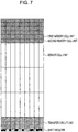
- FIG. 6 An exemplary layout of the photoelectric-conversion device illustrated in Fig. 3 is illustrated in each of Figs. 6 and 7 .
- a sensor-cell unit and two memory-cell units are grouped and the groups of the sensor-cell unit and the two memory-cell units are arranged in matrix-form.
- a transfer-circuit unit and a shift register are provided for each of lines including the sensor-cell units and the memory-cell units.
- Fig. 7 illustrates the layout including a separate region where only the sensor-cell units are provided and a separate region where only the memory-cell units are provided.
- the transfer-circuit unit and the shift register are provided for each of lines including the sensor-cell units and the memory-cell units.
- the present embodiment illustrates the operations of the photoelectric-conversion device, which are performed to determine whether or not a signal accumulated in the sensor-cell unit of each of the line-sensor units reaches a desired level (hereinafter referred to as the accumulation level) by specified time.
- the signal ⁇ FT is at low-level in a period (9').
- a signal S2(t1) + Nm1 obtained by adding the noise Nt of the transfer unit 113 to the signal S2(t1) - Nt + Nm1 described with reference to the period (8) illustrated in the first embodiment is written into the second memory-cell unit 102.
- the sign S2(t1) denotes a signal obtained at time t1, which is equivalent to the signal S2 described in the first embodiment.
- the signal ⁇ FB goes to low-level and the signal ⁇ FT goes to high-level in a period (10').
- the signals / ⁇ L and / ⁇ SL2_2 go to high-level in the period (10')
- the signal S2(t1) + Nm1 retained in the second memory-cell unit 102 is inverted and the noise Nm2 is added thereto.
- a signal - (S2(t1) + Nm1) + Nm2 is output to the common-output line 112.
- the buffer amplifier 123 upon receiving the signal ⁇ H transmitted from a shift register (not shown), the buffer amplifier 123 transmits the signal ⁇ H to a signal-processing unit (not shown).
- the signal-processing unit determines whether or not the signal read at the time t1 via the buffer amplifier 123 in the above-described manner reaches the accumulation level.
- the noise Nm2 - Nm1 superimposed on the read signal is sufficiently small compared to the level of the signal S2 for monitoring. Therefore, the signal is less affected by the noise.
- the operations equivalent to those performed in the periods (8') to (11') are performed again and a signal read at time t2 is output from the second memory-cell unit 102. From then on, the above-described operations are repeatedly performed until an acquired signal reaches the specified accumulation-finish level.
- the specified accumulation-finish level may be set based on purposes.
- the signals are repeatedly read from the second memory-cell unit 102 based on the noise 2 x Nt retained in the first memory-cell unit 101 so that the signal level can be monitored through the signal-processing unit provided in the stage subsequent to the buffer amplifier. Since the signal-processing unit can be provided in the stage subsequent to the buffer amplifier, the signal-processing unit is provided on a semiconductor substrate different from that of the line-sensor units, which makes it easier to lay out the line-sensor units.
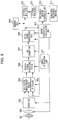
- FIG. 8 is a block diagram illustrating an exemplary configuration of a photoelectric-conversion device according to an embodiment of the present invention, where the photoelectric-conversion device is used for a phase-difference detection-type focus-detection device (hereinafter referred to as an AF sensor).
- AF sensor phase-difference detection-type focus-detection device
- An AF sensor 811 includes a sensor block provided with an arrangement of the line-sensor units L1A, L2A, ..., L1B, L2B, and so forth, a logic block 801 having an external interface and the function of generating a timing signal provided for the AF sensor 811, and an analog-circuit block 810.
- the analog-circuit block 810 includes AGC circuits 802, 803, 804, and 805, and monitors a signal transmitted from the line-sensor unit and/or controls the accumulation time.
- the analog-circuit block 810 further includes a reference voltage-and-current generation circuit 806 configured to generate a reference voltage and/or a reference current used for the photoelectric-conversion device, a thermometer circuit 807, and so forth.
- the logic block 801 performs serial communications with the outside via a serial-communication terminal 812 to control the drive timing of the AF sensor 811.
- the focus-detection operation can also be performed with high speed through the use of the photoelectric-conversion device described in each of the first and second embodiments.
- Fig. 9 is a block diagram illustrating an exemplary configuration of an image pickup system according to a fourth embodiment of the present invention.
- a barrier 901 configured to protect a lens which will be described later, a lens 902 configured to form the optical image of a subject in a solid-state image pickup device 904, and an aperture 903 configured to adjust the amount of light that had passed through the lens 902 are provided.
- the solid-state image pickup device 904 acquires the optical image of the object, which is formed through the lens 902, as an image signal.
- An AF sensor 905 includes the photoelectric-conversion device described in each of the above-described embodiments.
- An analog-signal processing device 906 configured to process a signal output from the solid-state image pickup device 904 and/or the AF sensor 905, and an analog-to-digital (A/D) converter 907 configured to perform the A/D conversion for a signal output from the analog-signal processing device 906 are provided.
- a digital-signal processing unit 908 is provided to perform various types of correction and/or compress image data output from the A/D converter 907.
- a memory unit 909 configured to temporarily store the image data, an external I/F circuit 910 configured to communicate with an external computer, for example, and a timing-generation unit 911 configured to output various types of timing signals to, for example, the digital-signal processing unit 908 are provided.
- An entire control-and-calculation unit 912 configured to perform various types of calculations and control the entire camera, a recording-medium control I/F unit 913, a removable recording medium 914, which includes a semiconductor memory or the like, configured to record and/or read acquired image data, and an external computer 915 are provided.
- the barrier 901 is opened and the entire control-and-calculation unit 912 calculates the distance from the image pickup system to the subject through the above-described phase-difference detection based on the signal output from the AF sensor 905. Then, the lens 902 is driven based on the calculation result, and it is determined whether or not focusing is achieved again. If it is determined that no focusing is achieved, autofocus control is performed to drive the lens 902 again. Then, the solid-state image pickup device 904 starts performing the accumulation operation after the focusing is confirmed.
- an image signal output from the solid-state image pickup device 904 is subjected to the A/D conversion through the A/D converter 907, passes through the digital-signal processing unit 908, and is written into the memory unit 909 through the entire control-and-calculation unit 912.
- data accumulated in the memory unit 909 is recorded onto the recording medium 914 via the recording-medium control I/F unit 913 under the control of the entire control-and-calculation unit 912. Otherwise, the data accumulated in the memory unit 909 may be directly transmitted to a computer or the like via the external I/F unit 910.
Landscapes
- Engineering & Computer Science (AREA)
- Multimedia (AREA)
- Signal Processing (AREA)
- Transforming Light Signals Into Electric Signals (AREA)
- Solid State Image Pick-Up Elements (AREA)
- Focusing (AREA)
- Studio Devices (AREA)
- Photometry And Measurement Of Optical Pulse Characteristics (AREA)
Claims (7)
- Dispositif comprenant :une pluralité de pixels unitaires (11A et 12A), chacun des pixels unitaires comportant un moyen de cellule de capteur (100) qui est agencé pour délivrer en sortie un signal obtenu par conversion photoélectrique et un bruit de réinitialisation généré en raison de l'initialisation du moyen de cellule de capteur (100), et une pluralité de moyens de cellules de mémoire (101 et 102) ;un moyen de transfert (113) ; etune ligne de sortie commune (112) connectée à chacun de la pluralité de pixels unitaires,caractérisé en ce quele moyen de cellule de capteur et le moyen de transfert sont connectés l'un à l'autre par l'intermédiaire d'un premier noeud (N1) de la ligne de sortie commune, et chacun de la pluralité de moyens de cellules de mémoire est connecté au premier noeud (N1),le moyen de transfert est agencé pour recevoir un signal délivré en sortie à partir du moyen de cellule de capteur, et pour délivrer en sortie un signal indiquant une différence entre le signal reçu et un bruit du moyen de transfert, etun signal basé sur le bruit du moyen de transfert est écrit dans au moins deux de la pluralité de moyens de cellules de mémoire dans la même période.
- Dispositif selon la revendication 1, dans lequel le moyen de transfert est agencé pour recevoir le bruit de réinitialisation à partir du moyen de cellule de capteur, et pour transférer un signal basé sur le bruit de réinitialisation vers le moyen de cellule de capteur, et pour transférer un signal basé sur le bruit du moyen de transfert vers chacun des moyens de cellules de mémoire.
- Dispositif selon la revendication 2, dans lequel le bruit du moyen de transfert est inclus dans le bruit de réinitialisation.
- Dispositif selon l'une quelconque des revendications 1 à 3, dans lequel le moyen de cellule de capteur comporte un moyen de conversion photoélectrique (103) et un moyen d'amplification (M11, M12) agencé pour amplifier et délivrer en sortie une charge électrique générée dans le moyen de conversion photoélectrique.
- Dispositif selon la revendication 2, comprenant en outre :une paire de moyens de capteurs de ligne (L1A et L2A), chacun des moyens de capteurs de ligne comportant la pluralité de pixels unitaires (11A et 12A),dans lequel, lorsque le signal délivré en sortie à partir du pixel unitaire atteint un niveau de fin d'accumulation spécifié, le dispositif est agencé pour effectuer un traitement de différence entre le signal délivré en sortie à partir du moyen de cellule de capteur et le signal basé sur le bruit du moyen de transfert en utilisant l'un des moyens de cellules de mémoire (101 et 102) de chacun des pixels unitaires, vers lequel le signal basé sur le bruit du moyen de transfert est transféré à partir du moyen de transfert,dans lequel le dispositif est agencé pour détecter une quantité de défocalisation sur la base de signaux délivrés en sortie à partir d'une partie de régions de la paire des moyens de capteurs de ligne (L1A et L2A), etdans lequel le dispositif est agencé pour détecter une quantité de défocalisation sur la base de signaux délivrés en sortie à partir de toutes les régions de la paire des moyens de capteurs de ligne (L1A et L2A) et pour effectuer un traitement de différence entre le signal délivré en sortie à partir du moyen de cellule de capteur et le signal basé sur le bruit du moyen de transfert.
- Dispositif de détection de foyer de type à détection de différence de phase comportant le dispositif selon l'une quelconque des revendications 1 à 5.
- Système de capture d'image comprenant le dispositif de détection de foyer selon la revendication 6.
Applications Claiming Priority (1)
| Application Number | Priority Date | Filing Date | Title |
|---|---|---|---|
| JP2009278007A JP5441651B2 (ja) | 2009-12-07 | 2009-12-07 | 光電変換装置 |
Publications (3)
| Publication Number | Publication Date |
|---|---|
| EP2334055A2 EP2334055A2 (fr) | 2011-06-15 |
| EP2334055A3 EP2334055A3 (fr) | 2015-12-09 |
| EP2334055B1 true EP2334055B1 (fr) | 2017-03-01 |
Family
ID=43650332
Family Applications (1)
| Application Number | Title | Priority Date | Filing Date |
|---|---|---|---|
| EP10191141.0A Not-in-force EP2334055B1 (fr) | 2009-12-07 | 2010-11-15 | Dispositif de conversion photoélectrique |
Country Status (4)
| Country | Link |
|---|---|
| US (1) | US8786723B2 (fr) |
| EP (1) | EP2334055B1 (fr) |
| JP (1) | JP5441651B2 (fr) |
| CN (1) | CN102088576B (fr) |
Families Citing this family (4)
| Publication number | Priority date | Publication date | Assignee | Title |
|---|---|---|---|---|
| JP5578984B2 (ja) * | 2009-12-03 | 2014-08-27 | キヤノン株式会社 | 光電変換装置、焦点検出装置及び撮像システム |
| JP5868056B2 (ja) * | 2011-07-27 | 2016-02-24 | キヤノン株式会社 | 光電変換装置、焦点検出装置及び撮像システム |
| JP5967916B2 (ja) | 2011-08-09 | 2016-08-10 | キヤノン株式会社 | 焦点検出センサ及び焦点検出センサを用いた光学機器 |
| JP6057568B2 (ja) * | 2012-07-04 | 2017-01-11 | キヤノン株式会社 | 光電変換装置 |
Family Cites Families (19)
| Publication number | Priority date | Publication date | Assignee | Title |
|---|---|---|---|---|
| ES2211937T3 (es) * | 1995-08-02 | 2004-07-16 | Canon Kabushiki Kaisha | Dispositivo sensor de imagenes de estado solido con linea de salida comun. |
| JP3610144B2 (ja) * | 1996-01-19 | 2005-01-12 | キヤノン株式会社 | 固体撮像装置 |
| US6781624B1 (en) * | 1998-07-30 | 2004-08-24 | Canon Kabushiki Kaisha | Signal processing apparatus |
| US7009163B2 (en) * | 2001-06-22 | 2006-03-07 | Orbotech Ltd. | High-sensitivity optical scanning using memory integration |
| US6795117B2 (en) * | 2001-11-06 | 2004-09-21 | Candela Microsystems, Inc. | CMOS image sensor with noise cancellation |
| US7327393B2 (en) * | 2002-10-29 | 2008-02-05 | Micron Technology, Inc. | CMOS image sensor with variable conversion gain |
| US7692704B2 (en) * | 2003-12-25 | 2010-04-06 | Canon Kabushiki Kaisha | Imaging apparatus for processing noise signal and photoelectric conversion signal |
| JP5121120B2 (ja) * | 2005-02-08 | 2013-01-16 | キヤノン株式会社 | 焦点検出装置および光学機器 |
| JP5181423B2 (ja) * | 2006-03-20 | 2013-04-10 | ソニー株式会社 | 半導体メモリデバイスとその動作方法 |
| JP4442675B2 (ja) * | 2007-09-28 | 2010-03-31 | ソニー株式会社 | 画素駆動回路および撮像装置ならびにカメラシステム |
| JP4556993B2 (ja) * | 2007-12-07 | 2010-10-06 | セイコーエプソン株式会社 | 状態検査システム |
| JP5568880B2 (ja) * | 2008-04-03 | 2014-08-13 | ソニー株式会社 | 固体撮像装置、固体撮像装置の駆動方法および電子機器 |
| US8169540B2 (en) * | 2008-09-10 | 2012-05-01 | Panasonic Corporation | Compact camera body to which interchangeable lens unit is mountable |
| JP5212022B2 (ja) * | 2008-10-30 | 2013-06-19 | ソニー株式会社 | 固体撮像装置、撮像装置、画素駆動電圧適正化装置、画素駆動電圧適正化方法 |
| KR101700658B1 (ko) * | 2008-12-30 | 2017-02-01 | 삼성전자주식회사 | 초점 검출 장치가 구비된 일안 반사식 카메라 및 그의 촬영방법 |
| US8174602B2 (en) * | 2009-01-15 | 2012-05-08 | Raytheon Company | Image sensing system and method utilizing a MOSFET |
| KR20100084819A (ko) * | 2009-01-19 | 2010-07-28 | 삼성전자주식회사 | 파장검출장치 및 이를 구비하는 초점검출장치 |
| KR101588299B1 (ko) * | 2009-01-20 | 2016-01-25 | 삼성전자주식회사 | 수광량에 대한 실시간 모니터링이 가능한 4-Tr 타입의 AF 픽셀을 이용한 AF 모듈 및 이를 적용한 촬영장치 |
| JP5578984B2 (ja) * | 2009-12-03 | 2014-08-27 | キヤノン株式会社 | 光電変換装置、焦点検出装置及び撮像システム |
-
2009
- 2009-12-07 JP JP2009278007A patent/JP5441651B2/ja not_active Expired - Fee Related
-
2010
- 2010-11-15 EP EP10191141.0A patent/EP2334055B1/fr not_active Not-in-force
- 2010-12-01 US US12/958,238 patent/US8786723B2/en not_active Expired - Fee Related
- 2010-12-07 CN CN2010105757772A patent/CN102088576B/zh not_active Expired - Fee Related
Non-Patent Citations (1)
| Title |
|---|
| None * |
Also Published As
| Publication number | Publication date |
|---|---|
| CN102088576A (zh) | 2011-06-08 |
| EP2334055A3 (fr) | 2015-12-09 |
| JP5441651B2 (ja) | 2014-03-12 |
| US20110134272A1 (en) | 2011-06-09 |
| JP2011120175A (ja) | 2011-06-16 |
| CN102088576B (zh) | 2013-10-23 |
| US8786723B2 (en) | 2014-07-22 |
| EP2334055A2 (fr) | 2011-06-15 |
Similar Documents
| Publication | Publication Date | Title |
|---|---|---|
| CN102158657B (zh) | 光电转换器件、焦点检测装置和图像拾取系统 | |
| US7554591B2 (en) | Photoelectric conversion apparatus and image sensing system using the same | |
| JP5173171B2 (ja) | 光電変換装置、撮像装置及び信号読出方法 | |
| US8319869B2 (en) | Solid-state imaging device | |
| US8698930B2 (en) | Photoelectric conversion apparatus, focus detection apparatus, and image pickup system | |
| JP4654046B2 (ja) | Cmosイメージセンサのクランプ回路 | |
| US8817156B2 (en) | Photoelectric conversion apparatus, focus detection apparatus, and image pickup system | |
| US8836837B2 (en) | Photoelectric conversion apparatus, focus detecting apparatus, and imaging system | |
| EP2334055B1 (fr) | Dispositif de conversion photoélectrique | |
| US8948584B2 (en) | Photoelectric conversion device and camera system | |
| US10116854B2 (en) | Photoelectric conversion apparatus, switching an electric path between a conductive state and a non-conductive state | |
| JP2008072324A (ja) | イメージセンサ、モジュール、および、電子機器 | |
| US8803054B2 (en) | Apparatus, focus detection apparatus, and image pickup system | |
| US8681252B2 (en) | Photoelectric conversion apparatus and image pickup system | |
| KR20150130186A (ko) | 이미지 센서 및 그 적층 구조 | |
| US20140009664A1 (en) | Photoelectric conversion apparatus | |
| JP5950967B2 (ja) | 光電変換装置、焦点検出装置及び撮像システム | |
| JP2006270182A (ja) | 固体撮像素子 |
Legal Events
| Date | Code | Title | Description |
|---|---|---|---|
| PUAI | Public reference made under article 153(3) epc to a published international application that has entered the european phase |
Free format text: ORIGINAL CODE: 0009012 |
|
| AK | Designated contracting states |
Kind code of ref document: A2 Designated state(s): AL AT BE BG CH CY CZ DE DK EE ES FI FR GB GR HR HU IE IS IT LI LT LU LV MC MK MT NL NO PL PT RO RS SE SI SK SM TR |
|
| AX | Request for extension of the european patent |
Extension state: BA ME |
|
| PUAL | Search report despatched |
Free format text: ORIGINAL CODE: 0009013 |
|
| AK | Designated contracting states |
Kind code of ref document: A3 Designated state(s): AL AT BE BG CH CY CZ DE DK EE ES FI FR GB GR HR HU IE IS IT LI LT LU LV MC MK MT NL NO PL PT RO RS SE SI SK SM TR |
|
| AX | Request for extension of the european patent |
Extension state: BA ME |
|
| RIC1 | Information provided on ipc code assigned before grant |
Ipc: H04N 5/3745 20110101ALI20151030BHEP Ipc: H04N 5/363 20110101AFI20151030BHEP Ipc: H04N 5/232 20060101ALI20151030BHEP |
|
| 17P | Request for examination filed |
Effective date: 20160609 |
|
| RBV | Designated contracting states (corrected) |
Designated state(s): AL AT BE BG CH CY CZ DE DK EE ES FI FR GB GR HR HU IE IS IT LI LT LU LV MC MK MT NL NO PL PT RO RS SE SI SK SM TR |
|
| GRAP | Despatch of communication of intention to grant a patent |
Free format text: ORIGINAL CODE: EPIDOSNIGR1 |
|
| INTG | Intention to grant announced |
Effective date: 20160909 |
|
| GRAS | Grant fee paid |
Free format text: ORIGINAL CODE: EPIDOSNIGR3 |
|
| GRAA | (expected) grant |
Free format text: ORIGINAL CODE: 0009210 |
|
| AK | Designated contracting states |
Kind code of ref document: B1 Designated state(s): AL AT BE BG CH CY CZ DE DK EE ES FI FR GB GR HR HU IE IS IT LI LT LU LV MC MK MT NL NO PL PT RO RS SE SI SK SM TR |
|
| REG | Reference to a national code |
Ref country code: GB Ref legal event code: FG4D |
|
| REG | Reference to a national code |
Ref country code: CH Ref legal event code: EP Ref country code: AT Ref legal event code: REF Ref document number: 872535 Country of ref document: AT Kind code of ref document: T Effective date: 20170315 |
|
| REG | Reference to a national code |
Ref country code: IE Ref legal event code: FG4D |
|
| REG | Reference to a national code |
Ref country code: DE Ref legal event code: R096 Ref document number: 602010040318 Country of ref document: DE |
|
| REG | Reference to a national code |
Ref country code: NL Ref legal event code: MP Effective date: 20170301 |
|
| REG | Reference to a national code |
Ref country code: LT Ref legal event code: MG4D |
|
| REG | Reference to a national code |
Ref country code: AT Ref legal event code: MK05 Ref document number: 872535 Country of ref document: AT Kind code of ref document: T Effective date: 20170301 |
|
| PG25 | Lapsed in a contracting state [announced via postgrant information from national office to epo] |
Ref country code: LT Free format text: LAPSE BECAUSE OF FAILURE TO SUBMIT A TRANSLATION OF THE DESCRIPTION OR TO PAY THE FEE WITHIN THE PRESCRIBED TIME-LIMIT Effective date: 20170301 Ref country code: FI Free format text: LAPSE BECAUSE OF FAILURE TO SUBMIT A TRANSLATION OF THE DESCRIPTION OR TO PAY THE FEE WITHIN THE PRESCRIBED TIME-LIMIT Effective date: 20170301 Ref country code: GR Free format text: LAPSE BECAUSE OF FAILURE TO SUBMIT A TRANSLATION OF THE DESCRIPTION OR TO PAY THE FEE WITHIN THE PRESCRIBED TIME-LIMIT Effective date: 20170602 Ref country code: HR Free format text: LAPSE BECAUSE OF FAILURE TO SUBMIT A TRANSLATION OF THE DESCRIPTION OR TO PAY THE FEE WITHIN THE PRESCRIBED TIME-LIMIT Effective date: 20170301 Ref country code: NO Free format text: LAPSE BECAUSE OF FAILURE TO SUBMIT A TRANSLATION OF THE DESCRIPTION OR TO PAY THE FEE WITHIN THE PRESCRIBED TIME-LIMIT Effective date: 20170601 |
|
| PG25 | Lapsed in a contracting state [announced via postgrant information from national office to epo] |
Ref country code: BG Free format text: LAPSE BECAUSE OF FAILURE TO SUBMIT A TRANSLATION OF THE DESCRIPTION OR TO PAY THE FEE WITHIN THE PRESCRIBED TIME-LIMIT Effective date: 20170601 Ref country code: ES Free format text: LAPSE BECAUSE OF FAILURE TO SUBMIT A TRANSLATION OF THE DESCRIPTION OR TO PAY THE FEE WITHIN THE PRESCRIBED TIME-LIMIT Effective date: 20170301 Ref country code: RS Free format text: LAPSE BECAUSE OF FAILURE TO SUBMIT A TRANSLATION OF THE DESCRIPTION OR TO PAY THE FEE WITHIN THE PRESCRIBED TIME-LIMIT Effective date: 20170301 Ref country code: LV Free format text: LAPSE BECAUSE OF FAILURE TO SUBMIT A TRANSLATION OF THE DESCRIPTION OR TO PAY THE FEE WITHIN THE PRESCRIBED TIME-LIMIT Effective date: 20170301 Ref country code: SE Free format text: LAPSE BECAUSE OF FAILURE TO SUBMIT A TRANSLATION OF THE DESCRIPTION OR TO PAY THE FEE WITHIN THE PRESCRIBED TIME-LIMIT Effective date: 20170301 Ref country code: AT Free format text: LAPSE BECAUSE OF FAILURE TO SUBMIT A TRANSLATION OF THE DESCRIPTION OR TO PAY THE FEE WITHIN THE PRESCRIBED TIME-LIMIT Effective date: 20170301 |
|
| PG25 | Lapsed in a contracting state [announced via postgrant information from national office to epo] |
Ref country code: NL Free format text: LAPSE BECAUSE OF FAILURE TO SUBMIT A TRANSLATION OF THE DESCRIPTION OR TO PAY THE FEE WITHIN THE PRESCRIBED TIME-LIMIT Effective date: 20170301 |
|
| PG25 | Lapsed in a contracting state [announced via postgrant information from national office to epo] |
Ref country code: RO Free format text: LAPSE BECAUSE OF FAILURE TO SUBMIT A TRANSLATION OF THE DESCRIPTION OR TO PAY THE FEE WITHIN THE PRESCRIBED TIME-LIMIT Effective date: 20170301 Ref country code: EE Free format text: LAPSE BECAUSE OF FAILURE TO SUBMIT A TRANSLATION OF THE DESCRIPTION OR TO PAY THE FEE WITHIN THE PRESCRIBED TIME-LIMIT Effective date: 20170301 Ref country code: CZ Free format text: LAPSE BECAUSE OF FAILURE TO SUBMIT A TRANSLATION OF THE DESCRIPTION OR TO PAY THE FEE WITHIN THE PRESCRIBED TIME-LIMIT Effective date: 20170301 Ref country code: SK Free format text: LAPSE BECAUSE OF FAILURE TO SUBMIT A TRANSLATION OF THE DESCRIPTION OR TO PAY THE FEE WITHIN THE PRESCRIBED TIME-LIMIT Effective date: 20170301 Ref country code: IT Free format text: LAPSE BECAUSE OF FAILURE TO SUBMIT A TRANSLATION OF THE DESCRIPTION OR TO PAY THE FEE WITHIN THE PRESCRIBED TIME-LIMIT Effective date: 20170301 |
|
| PG25 | Lapsed in a contracting state [announced via postgrant information from national office to epo] |
Ref country code: PT Free format text: LAPSE BECAUSE OF FAILURE TO SUBMIT A TRANSLATION OF THE DESCRIPTION OR TO PAY THE FEE WITHIN THE PRESCRIBED TIME-LIMIT Effective date: 20170703 Ref country code: PL Free format text: LAPSE BECAUSE OF FAILURE TO SUBMIT A TRANSLATION OF THE DESCRIPTION OR TO PAY THE FEE WITHIN THE PRESCRIBED TIME-LIMIT Effective date: 20170301 Ref country code: IS Free format text: LAPSE BECAUSE OF FAILURE TO SUBMIT A TRANSLATION OF THE DESCRIPTION OR TO PAY THE FEE WITHIN THE PRESCRIBED TIME-LIMIT Effective date: 20170701 Ref country code: SM Free format text: LAPSE BECAUSE OF FAILURE TO SUBMIT A TRANSLATION OF THE DESCRIPTION OR TO PAY THE FEE WITHIN THE PRESCRIBED TIME-LIMIT Effective date: 20170301 |
|
| REG | Reference to a national code |
Ref country code: DE Ref legal event code: R097 Ref document number: 602010040318 Country of ref document: DE |
|
| PLBE | No opposition filed within time limit |
Free format text: ORIGINAL CODE: 0009261 |
|
| STAA | Information on the status of an ep patent application or granted ep patent |
Free format text: STATUS: NO OPPOSITION FILED WITHIN TIME LIMIT |
|
| PG25 | Lapsed in a contracting state [announced via postgrant information from national office to epo] |
Ref country code: DK Free format text: LAPSE BECAUSE OF FAILURE TO SUBMIT A TRANSLATION OF THE DESCRIPTION OR TO PAY THE FEE WITHIN THE PRESCRIBED TIME-LIMIT Effective date: 20170301 |
|
| 26N | No opposition filed |
Effective date: 20171204 |
|
| PG25 | Lapsed in a contracting state [announced via postgrant information from national office to epo] |
Ref country code: SI Free format text: LAPSE BECAUSE OF FAILURE TO SUBMIT A TRANSLATION OF THE DESCRIPTION OR TO PAY THE FEE WITHIN THE PRESCRIBED TIME-LIMIT Effective date: 20170301 |
|
| PG25 | Lapsed in a contracting state [announced via postgrant information from national office to epo] |
Ref country code: MC Free format text: LAPSE BECAUSE OF FAILURE TO SUBMIT A TRANSLATION OF THE DESCRIPTION OR TO PAY THE FEE WITHIN THE PRESCRIBED TIME-LIMIT Effective date: 20170301 |
|
| GBPC | Gb: european patent ceased through non-payment of renewal fee |
Effective date: 20171115 |
|
| PG25 | Lapsed in a contracting state [announced via postgrant information from national office to epo] |
Ref country code: LI Free format text: LAPSE BECAUSE OF NON-PAYMENT OF DUE FEES Effective date: 20171130 Ref country code: CH Free format text: LAPSE BECAUSE OF NON-PAYMENT OF DUE FEES Effective date: 20171130 |
|
| PG25 | Lapsed in a contracting state [announced via postgrant information from national office to epo] |
Ref country code: LU Free format text: LAPSE BECAUSE OF NON-PAYMENT OF DUE FEES Effective date: 20171115 |
|
| REG | Reference to a national code |
Ref country code: FR Ref legal event code: ST Effective date: 20180731 Ref country code: BE Ref legal event code: MM Effective date: 20171130 |
|
| REG | Reference to a national code |
Ref country code: IE Ref legal event code: MM4A |
|
| PG25 | Lapsed in a contracting state [announced via postgrant information from national office to epo] |
Ref country code: MT Free format text: LAPSE BECAUSE OF NON-PAYMENT OF DUE FEES Effective date: 20171115 |
|
| PG25 | Lapsed in a contracting state [announced via postgrant information from national office to epo] |
Ref country code: IE Free format text: LAPSE BECAUSE OF NON-PAYMENT OF DUE FEES Effective date: 20171115 Ref country code: FR Free format text: LAPSE BECAUSE OF NON-PAYMENT OF DUE FEES Effective date: 20171130 |
|
| PG25 | Lapsed in a contracting state [announced via postgrant information from national office to epo] |
Ref country code: BE Free format text: LAPSE BECAUSE OF NON-PAYMENT OF DUE FEES Effective date: 20171130 Ref country code: GB Free format text: LAPSE BECAUSE OF NON-PAYMENT OF DUE FEES Effective date: 20171115 |
|
| PG25 | Lapsed in a contracting state [announced via postgrant information from national office to epo] |
Ref country code: HU Free format text: LAPSE BECAUSE OF FAILURE TO SUBMIT A TRANSLATION OF THE DESCRIPTION OR TO PAY THE FEE WITHIN THE PRESCRIBED TIME-LIMIT; INVALID AB INITIO Effective date: 20101115 |
|
| PG25 | Lapsed in a contracting state [announced via postgrant information from national office to epo] |
Ref country code: CY Free format text: LAPSE BECAUSE OF NON-PAYMENT OF DUE FEES Effective date: 20170301 |
|
| PG25 | Lapsed in a contracting state [announced via postgrant information from national office to epo] |
Ref country code: MK Free format text: LAPSE BECAUSE OF FAILURE TO SUBMIT A TRANSLATION OF THE DESCRIPTION OR TO PAY THE FEE WITHIN THE PRESCRIBED TIME-LIMIT Effective date: 20170301 |
|
| PG25 | Lapsed in a contracting state [announced via postgrant information from national office to epo] |
Ref country code: TR Free format text: LAPSE BECAUSE OF FAILURE TO SUBMIT A TRANSLATION OF THE DESCRIPTION OR TO PAY THE FEE WITHIN THE PRESCRIBED TIME-LIMIT Effective date: 20170301 |
|
| PGFP | Annual fee paid to national office [announced via postgrant information from national office to epo] |
Ref country code: DE Payment date: 20200130 Year of fee payment: 10 |
|
| PG25 | Lapsed in a contracting state [announced via postgrant information from national office to epo] |
Ref country code: AL Free format text: LAPSE BECAUSE OF FAILURE TO SUBMIT A TRANSLATION OF THE DESCRIPTION OR TO PAY THE FEE WITHIN THE PRESCRIBED TIME-LIMIT Effective date: 20170301 |
|
| REG | Reference to a national code |
Ref country code: DE Ref legal event code: R119 Ref document number: 602010040318 Country of ref document: DE |
|
| PG25 | Lapsed in a contracting state [announced via postgrant information from national office to epo] |
Ref country code: DE Free format text: LAPSE BECAUSE OF NON-PAYMENT OF DUE FEES Effective date: 20210601 |