EP2324496B1 - Semiconductor device with isolation trench liner, and related fabrication methods - Google Patents
Semiconductor device with isolation trench liner, and related fabrication methods Download PDFInfo
- Publication number
- EP2324496B1 EP2324496B1 EP09791330.5A EP09791330A EP2324496B1 EP 2324496 B1 EP2324496 B1 EP 2324496B1 EP 09791330 A EP09791330 A EP 09791330A EP 2324496 B1 EP2324496 B1 EP 2324496B1
- Authority
- EP
- European Patent Office
- Prior art keywords
- layer
- gate
- liner
- trench
- overlying
- Prior art date
- Legal status (The legal status is an assumption and is not a legal conclusion. Google has not performed a legal analysis and makes no representation as to the accuracy of the status listed.)
- Active
Links
Images

Classifications
-
- H—ELECTRICITY
- H01—ELECTRIC ELEMENTS
- H01L—SEMICONDUCTOR DEVICES NOT COVERED BY CLASS H10
- H01L21/00—Processes or apparatus adapted for the manufacture or treatment of semiconductor or solid state devices or of parts thereof
- H01L21/70—Manufacture or treatment of devices consisting of a plurality of solid state components formed in or on a common substrate or of parts thereof; Manufacture of integrated circuit devices or of parts thereof
- H01L21/71—Manufacture of specific parts of devices defined in group H01L21/70
- H01L21/76—Making of isolation regions between components
- H01L21/762—Dielectric regions, e.g. EPIC dielectric isolation, LOCOS; Trench refilling techniques, SOI technology, use of channel stoppers
- H01L21/76224—Dielectric regions, e.g. EPIC dielectric isolation, LOCOS; Trench refilling techniques, SOI technology, use of channel stoppers using trench refilling with dielectric materials
- H01L21/76232—Dielectric regions, e.g. EPIC dielectric isolation, LOCOS; Trench refilling techniques, SOI technology, use of channel stoppers using trench refilling with dielectric materials of trenches having a shape other than rectangular or V-shape, e.g. rounded corners, oblique or rounded trench walls
-
- H—ELECTRICITY
- H01—ELECTRIC ELEMENTS
- H01L—SEMICONDUCTOR DEVICES NOT COVERED BY CLASS H10
- H01L21/00—Processes or apparatus adapted for the manufacture or treatment of semiconductor or solid state devices or of parts thereof
- H01L21/70—Manufacture or treatment of devices consisting of a plurality of solid state components formed in or on a common substrate or of parts thereof; Manufacture of integrated circuit devices or of parts thereof
- H01L21/71—Manufacture of specific parts of devices defined in group H01L21/70
- H01L21/76—Making of isolation regions between components
- H01L21/762—Dielectric regions, e.g. EPIC dielectric isolation, LOCOS; Trench refilling techniques, SOI technology, use of channel stoppers
- H01L21/7624—Dielectric regions, e.g. EPIC dielectric isolation, LOCOS; Trench refilling techniques, SOI technology, use of channel stoppers using semiconductor on insulator [SOI] technology
- H01L21/76264—SOI together with lateral isolation, e.g. using local oxidation of silicon, or dielectric or polycristalline material refilled trench or air gap isolation regions, e.g. completely isolated semiconductor islands
-
- H—ELECTRICITY
- H01—ELECTRIC ELEMENTS
- H01L—SEMICONDUCTOR DEVICES NOT COVERED BY CLASS H10
- H01L21/00—Processes or apparatus adapted for the manufacture or treatment of semiconductor or solid state devices or of parts thereof
- H01L21/70—Manufacture or treatment of devices consisting of a plurality of solid state components formed in or on a common substrate or of parts thereof; Manufacture of integrated circuit devices or of parts thereof
- H01L21/71—Manufacture of specific parts of devices defined in group H01L21/70
- H01L21/768—Applying interconnections to be used for carrying current between separate components within a device comprising conductors and dielectrics
- H01L21/76801—Applying interconnections to be used for carrying current between separate components within a device comprising conductors and dielectrics characterised by the formation and the after-treatment of the dielectrics, e.g. smoothing
- H01L21/76829—Applying interconnections to be used for carrying current between separate components within a device comprising conductors and dielectrics characterised by the formation and the after-treatment of the dielectrics, e.g. smoothing characterised by the formation of thin functional dielectric layers, e.g. dielectric etch-stop, barrier, capping or liner layers
- H01L21/76831—Applying interconnections to be used for carrying current between separate components within a device comprising conductors and dielectrics characterised by the formation and the after-treatment of the dielectrics, e.g. smoothing characterised by the formation of thin functional dielectric layers, e.g. dielectric etch-stop, barrier, capping or liner layers in via holes or trenches, e.g. non-conductive sidewall liners
-
- H—ELECTRICITY
- H01—ELECTRIC ELEMENTS
- H01L—SEMICONDUCTOR DEVICES NOT COVERED BY CLASS H10
- H01L21/00—Processes or apparatus adapted for the manufacture or treatment of semiconductor or solid state devices or of parts thereof
- H01L21/70—Manufacture or treatment of devices consisting of a plurality of solid state components formed in or on a common substrate or of parts thereof; Manufacture of integrated circuit devices or of parts thereof
- H01L21/71—Manufacture of specific parts of devices defined in group H01L21/70
- H01L21/768—Applying interconnections to be used for carrying current between separate components within a device comprising conductors and dielectrics
- H01L21/76838—Applying interconnections to be used for carrying current between separate components within a device comprising conductors and dielectrics characterised by the formation and the after-treatment of the conductors
- H01L21/76841—Barrier, adhesion or liner layers
Definitions
- Embodiments of the subject matter described herein relate generally to semiconductor devices. More particularly, embodiments of the subject matter relate to the use of isolation regions between metal oxide semiconductor transistors.
- MOSFETs metal oxide semiconductor field effect transistors
- a MOS transistor may be realized as a p-type device (i.e., a PMOS transistor) or an n-type device (i.e., an NMOS transistor).
- a semiconductor device can include both PMOS and NMOS transistors, and such a device is commonly referred to as a complementary MOS or CMOS device.
- a MOS transistor includes a gate electrode as a control electrode that is formed over a semiconductor substrate, and spaced-apart source and drain regions formed within the semiconductor substrate and between which a current can flow.
- the source and drain regions are typically accessed via respective conductive contacts formed on the source and drain regions. Bias voltages applied to the gate electrode, the source contact, and the drain contact control the flow of current through a channel in the semiconductor substrate between the source and drain regions beneath the gate electrode. Conductive metal interconnects (plugs) formed in an insulating layer are typically used to deliver bias voltages to the gate, source, and drain contacts.
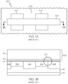
- FIG. 1 is a simplified diagram of a CMOS transistor device structure 100 that has been fabricated using conventional techniques.
- the upper portion of FIG. 1 (FIG. 1A ) represents a top view of device structure 100
- the lower portion of FIG. 1 (FIG. 1B ) represents a cross section of device structure 100 as viewed from line 1B-1B in the upper portion of FIG. 1 .
- Device structure 100 includes an n-type active region 102 of semiconductor material, a p-type active region 104 of semiconductor material, shallow trench isolation (STI) 106 surrounding and separating n-type region 102 and p-type region 104, and a gate structure 108 overlying n-type region 102, p-type region 104, and STI 106.
- STI shallow trench isolation
- Device structure 100 is formed on a silicon-on-insulator (SOI) substrate having a physical support substrate 110 and an insulating material 112 (typically a buried oxide) on support substrate 110.
- Gate structure 108 includes a gate insulator layer 114, which is formed from a dielectric material having a relatively high dielectric constant (i.e., a high- k material).
- Gate structure 108 also includes a gate metal layer 116 overlying gate insulator layer 114, and a layer of polycrystalline silicon 118 overlying gate metal layer 116.
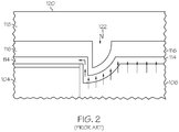
- FIG. 2 is a detailed view of a region 120 of device structure 100 (this region 120 is surrounded by the dashed circle in FIG. 1 ).
- FIG. 2 shows a divot 122 that can be formed as a result of one or more process steps that lead to the formation of device structure 100.
- Gate insulation layer 114, gate metal layer 116, and polycrystalline silicon 118 generally follow the contour of divot 122 as they are formed.
- the arrows in FIG. 2 represent the liberation of oxygen from STI 106 into gate insulator layer 114.
- the diffusion of oxygen through the high-k gate insulator layer 114 and over p-type region 104 causes the "width effect," which can degrade device performance.
- the oxygen also diffuses in over the adjacent n-type region, which would be located to the right of the portion of STI 106 shown in FIG. 2 .
- devices with shorter channel region lengths are more susceptible to the width effect.
- the width effect can be reduced using a number of known techniques.
- One known approach for reducing the width effect adds silicon to the high-k material. However, this adds control issues to dielectric deposition, and adversely impacts scaling.
- Another known approach for reducing the width effect employs nitridation of the high-k material. However, excess nitridation degrades device performance and can adversely affect the threshold voltage of the device.
- Yet another approach utilizes oxygen scavenging metals to create the metal gate layer. Unfortunately, oxygen scavenging metals have inherent control issues, which lead to excess variability in the process.
- the width effect can also be addressed by attempting to minimize the amount of overlap between the underlying STI material and the high-k gate material.
- One additional approach encapsulates the STI material with a nitride diffusion barrier prior to the deposition of the high-k material. This approach is unproven, and it leads to significant process complexity for the isolation module and variability to subsequent process modules.
- US 6,306,741 discloses a buffer layer and a gate dielectric layer overlying a substrate with at least one active area.
- the silicon substrate has shallow isolation trenches regions formed therein separating active area.
- a sacrificial oxide layer is formed over the gate dielectric layer and a nitride layer over that.
- a portion of the nitride layer and sacrificial oxide layer are patterned to form an opening exposing the underlying gate dielectric layer, on which a gate electrode is formed.
- the nitride layer and sacrificial oxide layers are then removed.
- a method of manufacturing a semiconductor device structure begins by providing a substrate having semiconductor material.
- An isolation trench is formed in the semiconductor material, and the trench is lined with a liner material that substantially inhibits formation of high-k material thereon.
- the lined trench is filled with an insulating material, over which is formed a layer of high-k gate material.
- the high-k gate material is formed such that it overlies at least a portion of the insulating material and at least a portion of the semiconductor material, and such that the layer of high-k gate material is divided by the liner material.
- a semiconductor device is also provided.
- the semiconductor device includes a layer of semiconductor material having an active transistor region defined therein, an isolation trench formed in the layer of semiconductor material adjacent to the active transistor region, a trench liner lining the isolation trench, an insulating material in the lined trench, and a layer of high-k gate material overlying at least a portion of the insulating material and overlying at least a portion of the active transistor region.
- the layer of high-k gate material is divided by the trench liner.
- a shallow trench isolation method for a semiconductor device structure in accordance with claim 1 and further comprising the steps recited in dependent claim 14.
- This method begins by providing a semiconductor substrate having a layer of semiconductor material, a pad oxide layer overlying the layer of semiconductor material, and a pad nitride layer overlying the pad oxide layer.
- the method then forms an isolation trench in the semiconductor substrate by selective removal of a portion of the pad nitride layer, a portion of the pad oxide layer, and a portion of the layer of semiconductor material.
- a liner material is deposited in the isolation trench and on exposed portions of the pad nitride layer, wherein the liner material substantially inhibits nucleation of high-k material thereon.
- an insulating material is deposited over the liner material such that the insulating material fills the isolation trench.
- This method further comprises polishing the insulating material to a height approximately corresponding to the liner material overlying the pad nitride layer. It further comprises removing the pad nitride layer and a portion of the liner material, leaving the insulating material substantially intact, wherein the removing step forms an exposed upper rim of the liner material.
- This method further comprises depositing a high-k gate material over the insulating material, wherein the exposed upper rim of the liner material remains void of the high-k gate material.
- MOS transistor devices including NMOS transistor devices, PMOS transistor devices, and CMOS transistor devices.
- MOS device properly refers to a device having a metal gate electrode and an oxide gate insulator, that term will be used throughout to refer to any semiconductor device that includes a conductive gate electrode (whether metal or other conductive material) that is positioned over a gate insulator (whether oxide or other insulator) which, in turn, is positioned over a semiconductor substrate.
- a semiconductor device fabricated in accordance with this process includes an STI liner that serves as an oxygen migration barrier between the STI oxide material and the high-k gate insulator.
- the STI liner eliminates (or significantly reduces) the diffusion of oxygen into that portion of the high-k gate insulator that overlies the active transistor region, thus minimizing the impact of the phenomena known as the width effect.
- the STI liner material is selected such that the high-k material does not nucleate on the STI liner material, which causes the STI liner to separate the high-k gate insulator into a first section (located over the STI material) and a second section (located over the active transistor region).
- fabrication of a semiconductor device structure begins by providing an appropriate semiconductor substrate 200 having a layer of semiconductor material 202.
- This fabrication process represents one implementation of a trench isolation method that is suitable for use with a semiconductor device, such as a CMOS transistor device.
- semiconductor substrate 200 is realized as a silicon-on-insulator (SOI) substrate, where semiconductor material 202 is disposed on a layer of insulator material 204 that, in turn, is supported by a carrier layer 206. More specifically, semiconductor material 202 is a silicon material, and insulator material 204 is a buried oxide layer.
- SOI silicon-on-insulator
- semiconductor material 202 is a silicon material
- insulator material 204 is a buried oxide layer.
- the term "silicon material” is used herein to encompass the generally monocrystalline and relatively pure silicon materials typically used in the semiconductor industry.
- Semiconductor material 202 can originally be either N-type or P-type silicon, but is typically P-type, and semiconductor material 202 is subsequently doped in an appropriate manner to form active regions.
- insulator material 204 is realized as a layer of silicon oxide (SiO 2 ).
- the semiconductor device structure can be formed on a bulk silicon substrate rather than an SOI substrate.
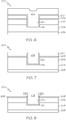
- FIG. 3 depicts semiconductor substrate 200 after formation of a pad oxide layer 208 on semiconductor material 202, and after formation of a pad nitride layer 210 on pad oxide layer 208.
- the resulting structure includes pad oxide layer 208 overlying semiconductor material 202, along with pad nitride layer 210 overlying pad oxide layer 208.
- Conventional process steps can be used to arrive at the structure depicted in FIG. 3 .
- pad oxide layer 208 is grown to the desired thickness, then pad nitride layer 210 is deposited over pad oxide layer 208 using an appropriate chemical vapor deposition (CVD) technique.
- CVD chemical vapor deposition
- isolation trench 212 can be formed by selectively removing a portion of pad nitride layer 210, a portion of pad oxide layer 208, and a portion of semiconductor material 202.
- formation of isolation trench 212 also involves the selective removal of a portion of insulator material 204 underlying semiconductor material 202.
- FIG. 4 depicts the state of semiconductor substrate 200 after completion of a number of known process steps, including photolithography, masking, and etching steps.
- isolation trench 212 extends into insulator material 204 to provide sufficient isolation between the portions of semiconductor material 202 on either side of isolation trench 212.
- liner material 214 can be deposited in isolation trench 212 and on any exposed portions of pad nitride layer 210 using any suitable technique, such as CVD, low pressure CVD (LPCVD), or plasma enhanced CVD (PECVD). Although preferred embodiments utilize a CVD material, liner material 214 could be a thermally grown material in alternate embodiments. Notably, liner material 214 is a material that substantially inhibits formation of high-k materials thereon.
- liner material 214 is such that high-k materials (the deposition of which is highly surface selective) do not nucleate on exposed surfaces of liner material 214.
- liner material 214 is a dielectric material such as a nitride, preferably, silicon nitride, and liner material 214 is formed with a typical thickness of about 20-100 Angstroms.
- liner material 214 forms a lined trench 216 in semiconductor substrate 200.
- this example continues by at least partially filling lined trench 216 with a suitable insulating material, referred to herein as STI material 218 ( FIG. 6 ).
- the dielectric STI material 218 fills lined trench 216 and is also formed over the other sections of liner material 214 (i.e., the sections overlying pad nitride layer 210) using, for example, an appropriate deposition technique such as CVD.
- STI material 218 is an oxide material, such as silicon dioxide deposited using tetraethyl orthosilicate (TEOS) as a silicon source (commonly referred to as TEOS oxide).
- TEOS tetraethyl orthosilicate
- silane is a very common precursor for the silicon source, and the resulting STI material 218 is commonly referred to as high density plasma (HDP) oxide.
- HDP high density plasma
- STI material 218 creates a filled isolation trench 220 in semiconductor substrate 200. Thereafter, STI material 218 is polished using, for example, a chemical mechanical polishing (CMP) tool. STI material 218 is preferably polished to a height approximately corresponding to the height of the liner material 214 overlying pad nitride layer 210. In practice, the nitride liner material 214 may serve as a CMP stop layer such that the top of STI material 218 is substantially continuous with the exposed surface of liner material 214.
- FIG. 7 illustrates the condition of semiconductor substrate 200 after STI material 218 has been polished or planarized to the desired height.
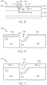
- this example continues by removing pad nitride layer 210 and a portion of liner material 214, while leaving STI material 218 substantially intact ( FIG. 8 ).
- the nitride and liner material can be removed using a technique that is selective to nitride, for example, a hot phosphoric acid strip. As depicted in FIG. 8 , this step is controlled such that pad nitride layer 210 is completely removed and such that an exposed upper rim 222 of liner material 214 remains. Referring again to the top view of FIG. 1 , upper rim 222 would roughly correspond to the boundary defined by the outline of region 102 or region 104. The selective nature of this stripping step ensures that STI material 218 and pad oxide layer 208 are not removed. Accordingly, the portion of liner material 214 underlying STI material 218 is protected.
- FIG. 9 depicts the state of semiconductor substrate 200 after further processing that may be needed prior to formation of the gate stack.
- Such further process steps may include, without limitation: removing pad oxide layer 208; forming a layer of sacrificial oxide 224 that replaces pad oxide layer 208; forming well implants with sacrificial oxide 224 in place; and wet etching.
- These process steps recess the height of STI material 218, but leave liner material 214 substantially intact.
- STI material 218 may be subjected to an isotropic oxide etchant, resulting in divots 226 formed on the sides of STI material 218.
- upper rim 222 of liner material 214 remains uncovered and exposed after semiconductor substrate 200 reaches the state shown in FIG. 9 .
- FIG. 10 is a detailed view of a region 230 of semiconductor substrate 200 (this region 230 is surrounded by the dashed circle in FIG. 9 ). The scale used in FIG. 10 is exaggerated for ease of illustration.
- upper rim 222 corresponds to the height of interfacial insulator layer 228 in the illustrated embodiment
- liner material 214 may protrude above the height of interfacial insulator layer 228, or it may be level with the height of semiconductor material 202 and level with the height of STI material 218.
- interfacial insulator layer 2208 this example continues by forming a layer of high-k gate material 232 overlying at least a portion of semiconductor material 202 and overlying at least a portion of STI material 218.
- high-k gate material can be deposited using any suitable technique, such as atomic layer deposition (ALD) or atomic layer chemical vapor deposition (ALCVD), which enables selective deposition of the high-k material on interfacial insulator layer 228 and on STI material 218, while resulting in little to no deposition on upper rim 222 of liner material 214.
- ALD atomic layer deposition
- ACVD atomic layer chemical vapor deposition
- high-k gate material 232 can be any material having a high dielectric constant relative to silicon dioxide, and such high-k materials are well known in the semiconductor industry.
- high-k gate material 232 may be, without limitation: HfO 2 , ZrO 2 , HfZrOx, HfSiOx, HfSiON, HfTiOx, ZrTiOx, ZrSiOx, ZrSiON, HfLaOx, ZrLaOx, LaAlOx, La 2 O 3 , HfAlOx, ZrAlOx, Al 2 O 3 , Y 2 O 3 , MgO, DyO, TiO 2 , Ta 2 O 5 , or the like.
- High-k gate material 232 is preferably deposited to a thickness of about 14-22 Angstroms.
- liner material 214 is chosen to substantially inhibit nucleation of high-k materials thereon, and this property causes the exposed upper rim 222 to remain void (for all practical purposes) of high-k gate material 232, as depicted in FIG. 10 .
- the layer of high-k gate material 232 is divided by liner material 214, and liner material 214 creates a discontinuity in the layer of high-k gate material 232.
- the section of high-k material overlying interfacial insulator layer 228 terminates before it overlaps upper rim 222, and the section of high-k material overlying STI material 218 follows the contour of divot 226 and terminates at or near the sidewall of liner material 214.
- a metal gate layer 234 is formed over high-k gate material 232 and over the exposed portions of liner material 214 ( FIG. 11 ) and, thereafter, a polysilicon gate layer 236 is formed over metal gate layer 234 ( FIG. 12 ).
- metal gate layer 234 can and does form on the exposed surfaces of liner material 214. Accordingly, metal gate layer 234 generally follows the contour of high-k gate material 232 and liner material 214 near divot 226.
- polysilicon gate layer 236 is deposited to a desired thickness such that it fills divot 226, as shown in FIG. 12 .
- the arrows in FIG. 12 represent the liberation of oxygen from STI material 218 into high-k gate material 232.
- the oxygen does not migrate or diffuse into the section of high-k gate material 232 that overlies semiconductor material 202.
- liner material 214 blocks the migration of oxygen from the section of high-k gate material 232 that overlies STI material 218. Consequently, liner material 214 can be used to reduce the width effect, which might otherwise degrade device performance (as explained above). It should be appreciated that even if a very thin layer of high-k gate material 232 forms on liner material 214, the migration of oxygen will be substantially impeded and, therefore, the same benefits will be obtained.
- any number of known process steps can be performed to complete the fabrication of the device structures.
- the process techniques described herein can be utilized with a "gate first” process or with a “gate last” process (which replaces polysilicon gate layer 236 with a different metal material).
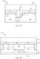
- FIG. 13 is a cross sectional view of a semiconductor device 300 fabricated in accordance with the process depicted in FIGS. 3-12 . Most of the features and characteristics of semiconductor device 300 are similar or identical to those described above with reference to FIGS. 3-12 , and such common features and characteristics will not be redundantly described in detail here.
- This embodiment of semiconductor device 300 is formed on an SOI substrate 302 having a support layer 304 and a buried oxide layer 306 overlying support layer 304.
- the layer of semiconductor material overlying buried oxide layer 306 has active transistor regions defined therein;
- FIG. 13 depicts an n-type active transistor region 308 and a p-type active transistor region 310.
- the active transistor regions 308 and 310 are separated by an adjacent isolation trench 312, which is formed in the layer of semiconductor material and in buried oxide layer 306.
- Isolation trench 312 is lined with a trench liner 314 (e.g., a nitride material), and an insulating material such as an STI oxide 316 is located in the lined trench.
- Semiconductor device 300 also includes a layer of high-k gate material 318 overlying at least a portion of STI oxide 316 and overlying at least a portion of active transistor regions 308 and 310. It is important to note that the layer of high-k gate material 318 is divided by trench liner 314 because, as described above, the high-k gate material 318 cannot nucleate on the upper rim of trench liner 314.
- interfacial oxide layer between high-k gate material 318 and the active transistor regions 308 and 310 (see FIG. 12 ), and the divots on either side of STI oxide 316, are not shown in FIG. 13 .
- Semiconductor device 300 also includes a metal gate layer 320 overlying high-k gate material 318, and overlying the upper rim of trench liner 314.
- semiconductor device 300 includes a polysilicon gate layer 322 overlying metal gate layer 320.
- the combination of high-k gate material 318, metal gate layer 320, and polysilicon gate layer 322 may be referred to as a gate stack or a gate structure.
- the gate stack cooperates with active transistor regions 308 and 310 in a conventional manner to form NMOS and PMOS transistor devices.
- a semiconductor device may employ a layer of high-k material that is formed in an alternative manner that still reduces the width effect.
- the high-k material can be formed using a suitably controlled plasma vapor deposition (PVD) technique.
- PVD plasma vapor deposition
- the PVD process will naturally form the high-k material over the exposed surface of the interfacial oxide and over the exposed surface of the STI oxide.
- the amount of high-k material formed on the vertical sidewall of the divot (see FIG. 2 ) will be significantly less than the amount of high-k material formed elsewhere. Consequently, the very thin layer of high-k material on this sidewall of the divot will impede the migration of oxygen from the STI oxide side to the side overlying the active transistor region.
Landscapes
- Engineering & Computer Science (AREA)
- Physics & Mathematics (AREA)
- Condensed Matter Physics & Semiconductors (AREA)
- General Physics & Mathematics (AREA)
- Manufacturing & Machinery (AREA)
- Computer Hardware Design (AREA)
- Microelectronics & Electronic Packaging (AREA)
- Power Engineering (AREA)
- Element Separation (AREA)
- Metal-Oxide And Bipolar Metal-Oxide Semiconductor Integrated Circuits (AREA)
- Insulated Gate Type Field-Effect Transistor (AREA)
- Thin Film Transistor (AREA)
Applications Claiming Priority (2)
| Application Number | Priority Date | Filing Date | Title |
|---|---|---|---|
| US12/199,616 US7998832B2 (en) | 2008-08-27 | 2008-08-27 | Semiconductor device with isolation trench liner, and related fabrication methods |
| PCT/US2009/053271 WO2010025024A1 (en) | 2008-08-27 | 2009-08-10 | Semiconductor device with isolation trench liner, and related fabrication methods |
Publications (2)
| Publication Number | Publication Date |
|---|---|
| EP2324496A1 EP2324496A1 (en) | 2011-05-25 |
| EP2324496B1 true EP2324496B1 (en) | 2018-10-10 |
Family
ID=41202835
Family Applications (1)
| Application Number | Title | Priority Date | Filing Date |
|---|---|---|---|
| EP09791330.5A Active EP2324496B1 (en) | 2008-08-27 | 2009-08-10 | Semiconductor device with isolation trench liner, and related fabrication methods |
Country Status (6)
| Country | Link |
|---|---|
| US (3) | US7998832B2 (enExample) |
| EP (1) | EP2324496B1 (enExample) |
| JP (1) | JP5619003B2 (enExample) |
| KR (2) | KR101810111B1 (enExample) |
| CN (1) | CN102132397B (enExample) |
| WO (1) | WO2010025024A1 (enExample) |
Families Citing this family (25)
| Publication number | Priority date | Publication date | Assignee | Title |
|---|---|---|---|---|
| CN101375388B (zh) * | 2006-01-18 | 2011-08-03 | Nxp股份有限公司 | 金属线之间的自对准沟槽的集成 |
| JP2010199156A (ja) * | 2009-02-23 | 2010-09-09 | Panasonic Corp | 半導体装置及びその製造方法 |
| US20110014726A1 (en) * | 2009-07-20 | 2011-01-20 | Taiwan Semiconductor Manufacturing Company, Ltd. | Method of forming shallow trench isolation structure |
| US8716095B2 (en) * | 2010-06-03 | 2014-05-06 | Institute of Microelectronics, Chinese Academy of Sciences | Manufacturing method of gate stack and semiconductor device |
| US8680644B2 (en) * | 2011-04-11 | 2014-03-25 | International Business Machines Coroporation | Semiconductor device and method for making same |
| US8530312B2 (en) | 2011-08-08 | 2013-09-10 | Micron Technology, Inc. | Vertical devices and methods of forming |
| FR2981793A1 (fr) * | 2011-10-25 | 2013-04-26 | St Microelectronics Crolles 2 | Procede de fabrication de transistors a grille isolee |
| US8564074B2 (en) * | 2011-11-29 | 2013-10-22 | International Business Machines Corporation | Self-limiting oxygen seal for high-K dielectric and design structure |
| US9536993B2 (en) * | 2012-03-23 | 2017-01-03 | Japan Science And Technology Agency | Thin film transistor and method for manufacturing thin film transistor |
| US20130341762A1 (en) * | 2012-06-20 | 2013-12-26 | Macronix International Co., Ltd. | Semiconductor hole structure |
| US8673738B2 (en) | 2012-06-25 | 2014-03-18 | International Business Machines Corporation | Shallow trench isolation structures |
| JP6033594B2 (ja) * | 2012-07-18 | 2016-11-30 | 国立大学法人北陸先端科学技術大学院大学 | 薄膜トランジスタ及び薄膜トランジスタの製造方法 |
| KR20140059107A (ko) * | 2012-11-07 | 2014-05-15 | 주식회사 유피케미칼 | 실리콘 질화물 박막 제조 방법 |
| US8900952B2 (en) | 2013-03-11 | 2014-12-02 | International Business Machines Corporation | Gate stack including a high-k gate dielectric that is optimized for low voltage applications |
| US20140315371A1 (en) * | 2013-04-17 | 2014-10-23 | International Business Machines Corporation | Methods of forming isolation regions for bulk finfet semiconductor devices |
| US9679917B2 (en) | 2014-12-23 | 2017-06-13 | International Business Machines Corporation | Semiconductor structures with deep trench capacitor and methods of manufacture |
| US9991124B2 (en) * | 2015-01-20 | 2018-06-05 | Taiwan Semiconductor Manufacturing Company Ltd. | Metal gate and manufacturing method thereof |
| KR102271239B1 (ko) | 2015-03-23 | 2021-06-29 | 삼성전자주식회사 | 반도체 장치 및 이의 제조 방법 |
| US9865703B2 (en) | 2015-12-31 | 2018-01-09 | International Business Machines Corporation | High-K layer chamfering to prevent oxygen ingress in replacement metal gate (RMG) process |
| DE102018107908B4 (de) * | 2017-07-28 | 2023-01-05 | Taiwan Semiconductor Manufacturing Co., Ltd. | Verfahren zum Bilden eines integrierten Schaltkreises mit einer Versiegelungsschicht zum Bilden einer Speicherzellenstruktur in Logik- oder BCD-Technologie sowie ein integrierter Schaltkreis mit einer Dummy-Struktur an einer Grenze einer Vorrichtungsregion |
| US10504912B2 (en) * | 2017-07-28 | 2019-12-10 | Taiwan Semiconductor Manufacturing Co., Ltd. | Seal method to integrate non-volatile memory (NVM) into logic or bipolar CMOS DMOS (BCD) technology |
| CN110707086B (zh) * | 2018-10-09 | 2022-02-18 | 联华电子股份有限公司 | 半导体元件 |
| TW202209688A (zh) * | 2020-06-05 | 2022-03-01 | 日商Flosfia股份有限公司 | 半導體裝置 |
| KR20220085482A (ko) | 2020-12-15 | 2022-06-22 | 삼성전자주식회사 | 반도체 소자 |
| CN117156850A (zh) * | 2022-05-18 | 2023-12-01 | 联华电子股份有限公司 | 半导体元件及其制作方法 |
Citations (1)
| Publication number | Priority date | Publication date | Assignee | Title |
|---|---|---|---|---|
| US6306741B1 (en) * | 2000-07-13 | 2001-10-23 | Chartered Semiconductor Manufacturing, Inc. | Method of patterning gate electrodes with high K gate dielectrics |
Family Cites Families (16)
| Publication number | Priority date | Publication date | Assignee | Title |
|---|---|---|---|---|
| KR100286736B1 (ko) * | 1998-06-16 | 2001-04-16 | 윤종용 | 트렌치 격리 형성 방법 |
| KR100421046B1 (ko) | 2001-07-13 | 2004-03-04 | 삼성전자주식회사 | 반도체 장치 및 그 제조방법 |
| US6713335B2 (en) | 2002-08-22 | 2004-03-30 | Chartered Semiconductor Manufacturing Ltd. | Method of self-aligning a damascene gate structure to isolation regions |
| US6828211B2 (en) | 2002-10-01 | 2004-12-07 | Taiwan Semiconductor Manufacturing Co., Ltd. | Shallow trench filled with two or more dielectrics for isolation and coupling or for stress control |
| DE20308406U1 (de) * | 2003-05-28 | 2003-08-07 | Dekema Dental-Keramiköfen GmbH, 83395 Freilassing | Ofen für Zahnersatz oder -teilersatz |
| US7071515B2 (en) * | 2003-07-14 | 2006-07-04 | Taiwan Semiconductor Manufacturing Co., Ltd. | Narrow width effect improvement with photoresist plug process and STI corner ion implantation |
| US6940705B2 (en) * | 2003-07-25 | 2005-09-06 | Taiwan Semiconductor Manufacturing Company, Ltd. | Capacitor with enhanced performance and method of manufacture |
| US6936881B2 (en) * | 2003-07-25 | 2005-08-30 | Taiwan Semiconductor Manufacturing Company, Ltd. | Capacitor that includes high permittivity capacitor dielectric |
| JP3802530B2 (ja) * | 2003-12-12 | 2006-07-26 | 株式会社東芝 | 半導体装置及びその製造方法 |
| US7015113B2 (en) * | 2004-04-01 | 2006-03-21 | Micron Technology, Inc. | Methods of forming trench isolation regions |
| KR100672754B1 (ko) * | 2004-05-10 | 2007-01-22 | 주식회사 하이닉스반도체 | 트렌치형 소자분리막을 구비한 반도체 소자의 제조 방법 |
| US7160819B2 (en) * | 2005-04-25 | 2007-01-09 | Sharp Laboratories Of America, Inc. | Method to perform selective atomic layer deposition of zinc oxide |
| US20070003203A1 (en) * | 2005-06-30 | 2007-01-04 | Palmer Jeffrey D | Methods and apparatus for stripping optical fiber |
| US7586158B2 (en) * | 2005-07-07 | 2009-09-08 | Infineon Technologies Ag | Piezoelectric stress liner for bulk and SOI |
| US7229896B2 (en) * | 2005-08-03 | 2007-06-12 | United Microelectronics Corp. | STI process for eliminating silicon nitride liner induced defects |
| KR100764742B1 (ko) | 2006-06-16 | 2007-10-08 | 삼성전자주식회사 | 반도체 소자 및 그 제조 방법 |
-
2008
- 2008-08-27 US US12/199,616 patent/US7998832B2/en active Active
-
2009
- 2009-08-10 EP EP09791330.5A patent/EP2324496B1/en active Active
- 2009-08-10 CN CN200980134161.7A patent/CN102132397B/zh active Active
- 2009-08-10 KR KR1020177002051A patent/KR101810111B1/ko active Active
- 2009-08-10 JP JP2011525070A patent/JP5619003B2/ja active Active
- 2009-08-10 KR KR1020117006475A patent/KR101701360B1/ko active Active
- 2009-08-10 WO PCT/US2009/053271 patent/WO2010025024A1/en not_active Ceased
-
2011
- 2011-07-07 US US13/178,362 patent/US8217472B2/en active Active
-
2012
- 2012-05-16 US US13/473,175 patent/US8716828B2/en active Active
Patent Citations (1)
| Publication number | Priority date | Publication date | Assignee | Title |
|---|---|---|---|---|
| US6306741B1 (en) * | 2000-07-13 | 2001-10-23 | Chartered Semiconductor Manufacturing, Inc. | Method of patterning gate electrodes with high K gate dielectrics |
Also Published As
| Publication number | Publication date |
|---|---|
| WO2010025024A1 (en) | 2010-03-04 |
| KR20110102868A (ko) | 2011-09-19 |
| US20100052094A1 (en) | 2010-03-04 |
| US20120223399A1 (en) | 2012-09-06 |
| JP2012501542A (ja) | 2012-01-19 |
| JP5619003B2 (ja) | 2014-11-05 |
| KR20170013403A (ko) | 2017-02-06 |
| US8716828B2 (en) | 2014-05-06 |
| EP2324496A1 (en) | 2011-05-25 |
| KR101701360B1 (ko) | 2017-02-01 |
| US7998832B2 (en) | 2011-08-16 |
| KR101810111B1 (ko) | 2017-12-18 |
| CN102132397A (zh) | 2011-07-20 |
| US8217472B2 (en) | 2012-07-10 |
| US20110260263A1 (en) | 2011-10-27 |
| CN102132397B (zh) | 2016-06-29 |
Similar Documents
| Publication | Publication Date | Title |
|---|---|---|
| EP2324496B1 (en) | Semiconductor device with isolation trench liner, and related fabrication methods | |
| US7906381B2 (en) | Method for integrating silicon-on-nothing devices with standard CMOS devices | |
| US8907444B2 (en) | Stress-inducing structures, methods, and materials | |
| US8877606B2 (en) | Low cost fabrication of double box back gate silicon-on-insulator wafers with subsequent self aligned shallow trench isolation | |
| US9548356B2 (en) | Shallow trench isolation structures | |
| US20070164443A1 (en) | Semiconductor array and method for manufacturing a semiconductor array | |
| US6995447B2 (en) | Silicon on insulator device having trench isolation layer and method for manufacturing the same | |
| US8389392B2 (en) | FinFET with separate gates and method for fabricating a finFET with separate gates | |
| US7705417B2 (en) | Semiconductor device and method of fabricating isolation region | |
| US20010021567A1 (en) | Method of forming device isolation structure | |
| JPH10199968A (ja) | 半導体装置及び半導体装置の素子間分離溝の形成方法 | |
| US20120146152A1 (en) | Method of fabricating an integrated circuit having a strain inducing hollow trench isolation region | |
| US20060160294A1 (en) | Soi device with body contact self-aligned to gate | |
| US9978861B2 (en) | Semiconductor device having gate in trenches | |
| US7189619B2 (en) | Process for manufacturing vertically insulated structural components on SOI material of various thickness | |
| JP2006344959A (ja) | 半導体集積回路装置およびその製造方法 | |
| KR20010038596A (ko) | 반도체장치의 소자격리방법 | |
| US20100059852A1 (en) | Semiconductor transistor device with improved isolation arrangement, and related fabrication methods |
Legal Events
| Date | Code | Title | Description |
|---|---|---|---|
| PUAI | Public reference made under article 153(3) epc to a published international application that has entered the european phase |
Free format text: ORIGINAL CODE: 0009012 |
|
| 17P | Request for examination filed |
Effective date: 20110308 |
|
| AK | Designated contracting states |
Kind code of ref document: A1 Designated state(s): AT BE BG CH CY CZ DE DK EE ES FI FR GB GR HR HU IE IS IT LI LT LU LV MC MK MT NL NO PL PT RO SE SI SK SM TR |
|
| AX | Request for extension of the european patent |
Extension state: AL BA RS |
|
| DAX | Request for extension of the european patent (deleted) | ||
| 17Q | First examination report despatched |
Effective date: 20120809 |
|
| RAP1 | Party data changed (applicant data changed or rights of an application transferred) |
Owner name: CHENGDU HAIGUANG INTEGRATED CIRCUIT DESIGN CO., LT |
|
| GRAP | Despatch of communication of intention to grant a patent |
Free format text: ORIGINAL CODE: EPIDOSNIGR1 |
|
| STAA | Information on the status of an ep patent application or granted ep patent |
Free format text: STATUS: GRANT OF PATENT IS INTENDED |
|
| INTG | Intention to grant announced |
Effective date: 20180403 |
|
| GRAS | Grant fee paid |
Free format text: ORIGINAL CODE: EPIDOSNIGR3 |
|
| GRAA | (expected) grant |
Free format text: ORIGINAL CODE: 0009210 |
|
| STAA | Information on the status of an ep patent application or granted ep patent |
Free format text: STATUS: THE PATENT HAS BEEN GRANTED |
|
| AK | Designated contracting states |
Kind code of ref document: B1 Designated state(s): AT BE BG CH CY CZ DE DK EE ES FI FR GB GR HR HU IE IS IT LI LT LU LV MC MK MT NL NO PL PT RO SE SI SK SM TR |
|
| REG | Reference to a national code |
Ref country code: GB Ref legal event code: FG4D |
|
| REG | Reference to a national code |
Ref country code: CH Ref legal event code: EP Ref country code: AT Ref legal event code: REF Ref document number: 1052229 Country of ref document: AT Kind code of ref document: T Effective date: 20181015 |
|
| REG | Reference to a national code |
Ref country code: IE Ref legal event code: FG4D |
|
| REG | Reference to a national code |
Ref country code: DE Ref legal event code: R096 Ref document number: 602009055017 Country of ref document: DE |
|
| REG | Reference to a national code |
Ref country code: NL Ref legal event code: MP Effective date: 20181010 |
|
| REG | Reference to a national code |
Ref country code: LT Ref legal event code: MG4D |
|
| REG | Reference to a national code |
Ref country code: AT Ref legal event code: MK05 Ref document number: 1052229 Country of ref document: AT Kind code of ref document: T Effective date: 20181010 |
|
| PG25 | Lapsed in a contracting state [announced via postgrant information from national office to epo] |
Ref country code: NL Free format text: LAPSE BECAUSE OF FAILURE TO SUBMIT A TRANSLATION OF THE DESCRIPTION OR TO PAY THE FEE WITHIN THE PRESCRIBED TIME-LIMIT Effective date: 20181010 |
|
| PG25 | Lapsed in a contracting state [announced via postgrant information from national office to epo] |
Ref country code: ES Free format text: LAPSE BECAUSE OF FAILURE TO SUBMIT A TRANSLATION OF THE DESCRIPTION OR TO PAY THE FEE WITHIN THE PRESCRIBED TIME-LIMIT Effective date: 20181010 Ref country code: NO Free format text: LAPSE BECAUSE OF FAILURE TO SUBMIT A TRANSLATION OF THE DESCRIPTION OR TO PAY THE FEE WITHIN THE PRESCRIBED TIME-LIMIT Effective date: 20190110 Ref country code: AT Free format text: LAPSE BECAUSE OF FAILURE TO SUBMIT A TRANSLATION OF THE DESCRIPTION OR TO PAY THE FEE WITHIN THE PRESCRIBED TIME-LIMIT Effective date: 20181010 Ref country code: IS Free format text: LAPSE BECAUSE OF FAILURE TO SUBMIT A TRANSLATION OF THE DESCRIPTION OR TO PAY THE FEE WITHIN THE PRESCRIBED TIME-LIMIT Effective date: 20190210 Ref country code: BG Free format text: LAPSE BECAUSE OF FAILURE TO SUBMIT A TRANSLATION OF THE DESCRIPTION OR TO PAY THE FEE WITHIN THE PRESCRIBED TIME-LIMIT Effective date: 20190110 Ref country code: FI Free format text: LAPSE BECAUSE OF FAILURE TO SUBMIT A TRANSLATION OF THE DESCRIPTION OR TO PAY THE FEE WITHIN THE PRESCRIBED TIME-LIMIT Effective date: 20181010 Ref country code: LT Free format text: LAPSE BECAUSE OF FAILURE TO SUBMIT A TRANSLATION OF THE DESCRIPTION OR TO PAY THE FEE WITHIN THE PRESCRIBED TIME-LIMIT Effective date: 20181010 Ref country code: HR Free format text: LAPSE BECAUSE OF FAILURE TO SUBMIT A TRANSLATION OF THE DESCRIPTION OR TO PAY THE FEE WITHIN THE PRESCRIBED TIME-LIMIT Effective date: 20181010 Ref country code: PL Free format text: LAPSE BECAUSE OF FAILURE TO SUBMIT A TRANSLATION OF THE DESCRIPTION OR TO PAY THE FEE WITHIN THE PRESCRIBED TIME-LIMIT Effective date: 20181010 Ref country code: LV Free format text: LAPSE BECAUSE OF FAILURE TO SUBMIT A TRANSLATION OF THE DESCRIPTION OR TO PAY THE FEE WITHIN THE PRESCRIBED TIME-LIMIT Effective date: 20181010 |
|
| PG25 | Lapsed in a contracting state [announced via postgrant information from national office to epo] |
Ref country code: SE Free format text: LAPSE BECAUSE OF FAILURE TO SUBMIT A TRANSLATION OF THE DESCRIPTION OR TO PAY THE FEE WITHIN THE PRESCRIBED TIME-LIMIT Effective date: 20181010 Ref country code: PT Free format text: LAPSE BECAUSE OF FAILURE TO SUBMIT A TRANSLATION OF THE DESCRIPTION OR TO PAY THE FEE WITHIN THE PRESCRIBED TIME-LIMIT Effective date: 20190210 Ref country code: GR Free format text: LAPSE BECAUSE OF FAILURE TO SUBMIT A TRANSLATION OF THE DESCRIPTION OR TO PAY THE FEE WITHIN THE PRESCRIBED TIME-LIMIT Effective date: 20190111 |
|
| REG | Reference to a national code |
Ref country code: DE Ref legal event code: R097 Ref document number: 602009055017 Country of ref document: DE |
|
| PG25 | Lapsed in a contracting state [announced via postgrant information from national office to epo] |
Ref country code: CZ Free format text: LAPSE BECAUSE OF FAILURE TO SUBMIT A TRANSLATION OF THE DESCRIPTION OR TO PAY THE FEE WITHIN THE PRESCRIBED TIME-LIMIT Effective date: 20181010 Ref country code: DK Free format text: LAPSE BECAUSE OF FAILURE TO SUBMIT A TRANSLATION OF THE DESCRIPTION OR TO PAY THE FEE WITHIN THE PRESCRIBED TIME-LIMIT Effective date: 20181010 Ref country code: IT Free format text: LAPSE BECAUSE OF FAILURE TO SUBMIT A TRANSLATION OF THE DESCRIPTION OR TO PAY THE FEE WITHIN THE PRESCRIBED TIME-LIMIT Effective date: 20181010 |
|
| PLBE | No opposition filed within time limit |
Free format text: ORIGINAL CODE: 0009261 |
|
| STAA | Information on the status of an ep patent application or granted ep patent |
Free format text: STATUS: NO OPPOSITION FILED WITHIN TIME LIMIT |
|
| PG25 | Lapsed in a contracting state [announced via postgrant information from national office to epo] |
Ref country code: SK Free format text: LAPSE BECAUSE OF FAILURE TO SUBMIT A TRANSLATION OF THE DESCRIPTION OR TO PAY THE FEE WITHIN THE PRESCRIBED TIME-LIMIT Effective date: 20181010 Ref country code: RO Free format text: LAPSE BECAUSE OF FAILURE TO SUBMIT A TRANSLATION OF THE DESCRIPTION OR TO PAY THE FEE WITHIN THE PRESCRIBED TIME-LIMIT Effective date: 20181010 Ref country code: EE Free format text: LAPSE BECAUSE OF FAILURE TO SUBMIT A TRANSLATION OF THE DESCRIPTION OR TO PAY THE FEE WITHIN THE PRESCRIBED TIME-LIMIT Effective date: 20181010 Ref country code: SM Free format text: LAPSE BECAUSE OF FAILURE TO SUBMIT A TRANSLATION OF THE DESCRIPTION OR TO PAY THE FEE WITHIN THE PRESCRIBED TIME-LIMIT Effective date: 20181010 |
|
| 26N | No opposition filed |
Effective date: 20190711 |
|
| PG25 | Lapsed in a contracting state [announced via postgrant information from national office to epo] |
Ref country code: SI Free format text: LAPSE BECAUSE OF FAILURE TO SUBMIT A TRANSLATION OF THE DESCRIPTION OR TO PAY THE FEE WITHIN THE PRESCRIBED TIME-LIMIT Effective date: 20181010 |
|
| PG25 | Lapsed in a contracting state [announced via postgrant information from national office to epo] |
Ref country code: TR Free format text: LAPSE BECAUSE OF FAILURE TO SUBMIT A TRANSLATION OF THE DESCRIPTION OR TO PAY THE FEE WITHIN THE PRESCRIBED TIME-LIMIT Effective date: 20181010 |
|
| PG25 | Lapsed in a contracting state [announced via postgrant information from national office to epo] |
Ref country code: MC Free format text: LAPSE BECAUSE OF FAILURE TO SUBMIT A TRANSLATION OF THE DESCRIPTION OR TO PAY THE FEE WITHIN THE PRESCRIBED TIME-LIMIT Effective date: 20181010 Ref country code: LI Free format text: LAPSE BECAUSE OF NON-PAYMENT OF DUE FEES Effective date: 20190831 Ref country code: LU Free format text: LAPSE BECAUSE OF NON-PAYMENT OF DUE FEES Effective date: 20190810 Ref country code: CH Free format text: LAPSE BECAUSE OF NON-PAYMENT OF DUE FEES Effective date: 20190831 |
|
| REG | Reference to a national code |
Ref country code: BE Ref legal event code: MM Effective date: 20190831 |
|
| PG25 | Lapsed in a contracting state [announced via postgrant information from national office to epo] |
Ref country code: IE Free format text: LAPSE BECAUSE OF NON-PAYMENT OF DUE FEES Effective date: 20190810 |
|
| PG25 | Lapsed in a contracting state [announced via postgrant information from national office to epo] |
Ref country code: BE Free format text: LAPSE BECAUSE OF NON-PAYMENT OF DUE FEES Effective date: 20190831 |
|
| PG25 | Lapsed in a contracting state [announced via postgrant information from national office to epo] |
Ref country code: CY Free format text: LAPSE BECAUSE OF FAILURE TO SUBMIT A TRANSLATION OF THE DESCRIPTION OR TO PAY THE FEE WITHIN THE PRESCRIBED TIME-LIMIT Effective date: 20181010 |
|
| PG25 | Lapsed in a contracting state [announced via postgrant information from national office to epo] |
Ref country code: MT Free format text: LAPSE BECAUSE OF FAILURE TO SUBMIT A TRANSLATION OF THE DESCRIPTION OR TO PAY THE FEE WITHIN THE PRESCRIBED TIME-LIMIT Effective date: 20181010 Ref country code: HU Free format text: LAPSE BECAUSE OF FAILURE TO SUBMIT A TRANSLATION OF THE DESCRIPTION OR TO PAY THE FEE WITHIN THE PRESCRIBED TIME-LIMIT; INVALID AB INITIO Effective date: 20090810 |
|
| PG25 | Lapsed in a contracting state [announced via postgrant information from national office to epo] |
Ref country code: MK Free format text: LAPSE BECAUSE OF FAILURE TO SUBMIT A TRANSLATION OF THE DESCRIPTION OR TO PAY THE FEE WITHIN THE PRESCRIBED TIME-LIMIT Effective date: 20181010 |
|
| REG | Reference to a national code |
Ref country code: DE Ref legal event code: R082 Ref document number: 602009055017 Country of ref document: DE Representative=s name: RAVENSPAT PATENTANWAELTE PARTNERSCHAFT MBB, DE |
|
| PGFP | Annual fee paid to national office [announced via postgrant information from national office to epo] |
Ref country code: GB Payment date: 20250619 Year of fee payment: 17 |
|
| PGFP | Annual fee paid to national office [announced via postgrant information from national office to epo] |
Ref country code: FR Payment date: 20250610 Year of fee payment: 17 |
|
| PGFP | Annual fee paid to national office [announced via postgrant information from national office to epo] |
Ref country code: DE Payment date: 20250618 Year of fee payment: 17 |