EP2317541A2 - Verfahren zur Herstellung eines Halbleiterbauelements - Google Patents
Verfahren zur Herstellung eines Halbleiterbauelements Download PDFInfo
- Publication number
- EP2317541A2 EP2317541A2 EP10013772A EP10013772A EP2317541A2 EP 2317541 A2 EP2317541 A2 EP 2317541A2 EP 10013772 A EP10013772 A EP 10013772A EP 10013772 A EP10013772 A EP 10013772A EP 2317541 A2 EP2317541 A2 EP 2317541A2
- Authority
- EP
- European Patent Office
- Prior art keywords
- layer
- type
- formation region
- ion implantation
- semiconductor substrate
- Prior art date
- Legal status (The legal status is an assumption and is not a legal conclusion. Google has not performed a legal analysis and makes no representation as to the accuracy of the status listed.)
- Withdrawn
Links
Images


Classifications
-
- H—ELECTRICITY
- H10—SEMICONDUCTOR DEVICES; ELECTRIC SOLID-STATE DEVICES NOT OTHERWISE PROVIDED FOR
- H10D—INORGANIC ELECTRIC SEMICONDUCTOR DEVICES
- H10D84/00—Integrated devices formed in or on semiconductor substrates that comprise only semiconducting layers, e.g. on Si wafers or on GaAs-on-Si wafers
- H10D84/80—Integrated devices formed in or on semiconductor substrates that comprise only semiconducting layers, e.g. on Si wafers or on GaAs-on-Si wafers characterised by the integration of at least one component covered by groups H10D12/00 or H10D30/00, e.g. integration of IGFETs
- H10D84/811—Combinations of field-effect devices and one or more diodes, capacitors or resistors
-
- H—ELECTRICITY
- H10—SEMICONDUCTOR DEVICES; ELECTRIC SOLID-STATE DEVICES NOT OTHERWISE PROVIDED FOR
- H10D—INORGANIC ELECTRIC SEMICONDUCTOR DEVICES
- H10D1/00—Resistors, capacitors or inductors
- H10D1/40—Resistors
- H10D1/47—Resistors having no potential barriers
-
- H—ELECTRICITY
- H10—SEMICONDUCTOR DEVICES; ELECTRIC SOLID-STATE DEVICES NOT OTHERWISE PROVIDED FOR
- H10D—INORGANIC ELECTRIC SEMICONDUCTOR DEVICES
- H10D84/00—Integrated devices formed in or on semiconductor substrates that comprise only semiconducting layers, e.g. on Si wafers or on GaAs-on-Si wafers
- H10D84/40—Integrated devices formed in or on semiconductor substrates that comprise only semiconducting layers, e.g. on Si wafers or on GaAs-on-Si wafers characterised by the integration of at least one component covered by groups H10D12/00 or H10D30/00 with at least one component covered by groups H10D10/00 or H10D18/00, e.g. integration of IGFETs with BJTs
- H10D84/401—Combinations of FETs or IGBTs with BJTs
- H10D84/403—Combinations of FETs or IGBTs with BJTs and with one or more of diodes, resistors or capacitors
-
- H—ELECTRICITY
- H10—SEMICONDUCTOR DEVICES; ELECTRIC SOLID-STATE DEVICES NOT OTHERWISE PROVIDED FOR
- H10D—INORGANIC ELECTRIC SEMICONDUCTOR DEVICES
- H10D84/00—Integrated devices formed in or on semiconductor substrates that comprise only semiconducting layers, e.g. on Si wafers or on GaAs-on-Si wafers
- H10D84/80—Integrated devices formed in or on semiconductor substrates that comprise only semiconducting layers, e.g. on Si wafers or on GaAs-on-Si wafers characterised by the integration of at least one component covered by groups H10D12/00 or H10D30/00, e.g. integration of IGFETs
- H10D84/811—Combinations of field-effect devices and one or more diodes, capacitors or resistors
- H10D84/817—Combinations of field-effect devices and resistors only
Definitions
- the invention relates to a method of manufacturing a semiconductor device having a MOS transistor, a resistor element, etc on one semiconductor substrate.
- a resistor element and a bipolar transistor as well as a MOS transistor are integrated on one semiconductor substrate.
- the MOS transistor is used to form a logic circuit
- the resistor element is used as a feedback resistor for a crystal oscillator
- the bipolar transistor is used for a reference voltage generation circuit.
- a method of forming a MOS transistor and a resistor element on one semiconductor substrate is disclosed in Japanese Patent Application Publication No. 2001-110906 .
- a semiconductor device of the type described above includes elements such as a resistor element and a bipolar transistor as well as a MOS transistor, the number of masks and the number of manufacturing processes increase compared with a basic MOS process. It is an object of the invention to provide a less complex manufacturing.
- the invention provides a method of manufacturing a semiconductor device having a first MOS transistor with a channel of a first type and a resistor element that are formed on a semiconductor substrate.
- the method includes forming a first element isolation film isolating a first region of the semiconductor substrate on which the first MOS transistor is formed from other portions of the semiconductor substrate, and performing a first ion implantation to form a first channel stopper layer in the first region and to form at least preliminarily a resistor layer of the resistor element in a second region of the semiconductor substrate.
- the first channel stopper layer prevents a channel formation under the first element isolation film.
- the method also includes performing a second ion implantation to form a first punch-through prevention layer in the first region and to add impurities to the resistor layer.
- the first punch-through prevention layer prevents a punch-through of the first MOS transistor.
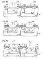
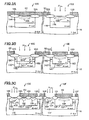
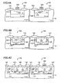
- Figs. 1A to 5C are cross-sectional views showing a method of manufacturing a semiconductor device of an embodiment of the invention.
- the solution according to the invention resides in the features of the independent claim and preferably in those of the dependent claims.
- a method of manufacturing a semiconductor device of an embodiment of the invention will be described referring to Figs. 1A to 5C .
- a MOS transistor, a resistor element and a bipolar transistor are formed on one semiconductor substrate, and A, B and C of Figs. 1A to 5C correspond to regions where the MOS transistor, the resistor element and the bipolar transistor are to be formed, respectively.
- the resistor element includes a first high resistor element having a sheet resistance value on the order of M ⁇ / square and a second high resistor element having a lower sheet resistance value than the first high resistor element.
- a P type well 11A is formed on the front surface of a P type semiconductor substrate 10.
- a P-channel type MOS transistor is to be formed in a region 10A where an N-channel type MOS transistor is to be formed in Fig. 1A
- an N type well 11B is formed on the front surface of the P type semiconductor substrate 10.
- the P type well 11A is formed by ion-implanting boron ion ( 11 B + ) in the semiconductor substrate 10 under a condition of acceleration energy of 60 KeV and a dose of 8.5 ⁇ 10 12 / cm 2 and then thermally diffusing this at about 1100 °C for eight hours, for example.
- the N type well 11B is formed at the same time as forming the P type well 11A by ion-implanting phosphorus ion ( 31 P + ) in the semiconductor substrate 10 under a condition of acceleration energy of 120 KeV and a dose of 7.5 ⁇ 10 12 / cm 2 and then performing the thermal diffusion mentioned above to this, for example.
- LOCOS film 12A is formed in the NMOS formation region 10A and a LOCOS film 12B is formed in the PMOS formation region 10B.
- the LOCOS films 12A, 12B are element isolation films that electrically isolate the corresponding PMOS and NMOS from the other elements respectively, and are formed so as to surround the P type well 11A and the N type well 11B as shown in the figure, for example.
- the invention is not limited to this, and these may be formed so as to have other planar pattern.
- N type wells 11C, 11D are respectively formed on the front surface of the P type semiconductor substrate 10.
- the N type wells 11C, 11D are formed by the same process as for the N type well 11B.
- a LOCOS film 12C is formed in the first high resistor element formation region 10C and a LOCOS film 12D is formed in the second high resistor element formation region 10D.
- the LOCOS films 12C, 12D are formed so as to surround the N type wells 11C, 11D, respectively, as shown in the figure, for example.
- the invention is not limited to this, and these may be formed so as to have other planar pattern.
- N type wells 11E, 11F are respectively formed on the front surface of the P type semiconductor substrate 10.
- the N type wells 11E, 11F are formed by the same process as for the N type well 11B.
- the N type wells 11E, 11F are to be the collector layers of the first BIP formation region 10E and the second BIP formation region 10F, respectively.
- LOCOS films 12E, 12G, 12H are formed in the first BIP formation region 10E, and LOCOS films 12I, 12F are formed in the second BIP formation region 10F.
- the whole PMOS formation region 10B is covered by a first resist R1, and a first ion implantation is performed to the P type well 11A through an opening of the first resist R1 provided in the NMOS formation region 10A.
- a P+ type channel stopper layer 14A is formed in the NMOS formation region 10A.
- a second ion implantation is further performed through the opening of the first resist R1 to form a P+ type punch-through prevention layer 13A.
- boron ion ( 11 B + ) is implanted in the P type well 11A under a condition of acceleration energy of 140 KeV and a dose of 3 ⁇ 10 12 / cm 2 .
- boron ion ( 11 B + ) is ion-implanted under such a condition as to penetrate the LOCOS film 12A.
- the channel stopper layer 14A is formed including under the LOCOS film 12A.
- This channel stopper layer 14A is a layer (an inversion prevention layer) that prevents a channel (an N type inversion layer) being formed due to the inversion of the conductivity type of the front surface of the P type well 11A under the LOCOS film 12A from P type to N type. Therefore, this channel stopper layer 14A functions enough as long as it is formed on the front surface of the P type well 11A at least under the LOCOS film 12A only. However, it is preferable that the channel stopper layer 14A is formed over the whole region in the P type well 11A where the NMOS is to be formed as shown in the figure since this achieves using the resist commonly in the first and second ion implantations.
- boron ion ( 11 B + ) is implanted in the P type well 11A under a condition of acceleration energy of 115 KeV and a dose of 8 ⁇ 10 12 / cm 2 .
- the punch-through prevention layer 13A is formed in the P type well 11A except under the LOCOS film 12A.
- This punch-through prevention layer 13A has a peak impurity concentration at a deeper position than the front surface of the channel region of the NMOS, and thus functions to prevent a leakage current due to a punch-through between the source and drain of the NMOS in the off state.
- the punch-through prevention layer 13A and the channel stopper layer 14A are formed using the same first resist R1 in the first and second ion implantation processes.
- the first and second ion implantations are utilized to form resistor layers 15C, 15D, respectively.
- the resist R1 has openings in the first high resistor element formation region 10C and the second high resistor element formation region 10D respectively, and boron ion ( 11 B + ) is implanted in the N type wells 11C, 11D through these openings by the first and second ion implantations.
- the P type resistor layer 15C including implantation layers 13C, 14C that are equivalent to the punch-through prevention layer 13A and the channel stopper layer 14A is formed in the N type well 11C.
- the P type resistor layer 15D including implantation layers 13D, 14D that are equivalent to the punch-through prevention layer 13A and the channel stopper layer 14A is formed in the N type well 11D.
- the first resist R1 is formed onto the LOCOS film 12C, 12D on the end portions of the N type wells 11C, 11D to prevent ion implantation in the end portions of the N type wells 11C, 11D.
- the P type resistor layers 15C, 15D are formed inside the N type wells 11C, 11D, respectively. Therefore, the resistor layers 15C, 15D are electrically isolated from the P type semiconductor substrate 10, and have potentials that are controllable independent of the potential of the semiconductor substrate 10.
- the first and second ion implantations are utilized to form P type base layers 15E, 15F.
- the first resist R1 has openings in the base layer formation regions, respectively, and boron ion ( 11 B + ) is implanted in the N type wells 11E, 11F through these openings by the first and second ion implantations.
- the P type base layer 15E including implantation layers 13E, 14E that are equivalent to the punch-through prevention layer 13A and the channel stopper layer 14A is formed in the N type well 11E.
- the P type base layer 15F including implantation layers 13F, 14F that are equivalent to the punch-through prevention layer 13A and the channel stopper layer 14A is formed in the N type well 11F.
- the punch-through prevention layer 13A, the channel stopper layer 14A, the resistor layers 15C, 15D, and the base layers 15E, 15F are formed using one mask (corresponding to the first resist R1).
- the whole NMOS formation region 10A is covered by a second resist R2, and a third ion implantation is performed to the N type well 11B through an opening of the second resist R2 provided in the PMOS formation region 10B.
- an N+ type channel stopper layer 17B is formed in the PMOS formation region 10B.
- a fourth ion implantation is performed through the opening of the second resist R2 to form an N+ type punch-through prevention layer 16B.
- phosphorus ion ( 31 p + ) is implanted in the N type well 11B under a condition of acceleration energy of 260 KeV and a dose of 6 ⁇ 10 12 / cm 2 .
- phosphorus ion ( 31 P + ) is ion-implanted under such a condition as to penetrate the LOCOS film 12B.
- the channel stopper layer 17B is formed including under the element isolation film 12B.
- This channel stopper layer 17B is a layer (an inversion prevention layer) that prevents a channel (a P type inversion layer) being formed due to the inversion of the conductivity type of the front surface of the N type well 11B under the LOCOS film 12B from N type to P type. Therefore, the channel stopper layer 17B functions enough as long as it is formed on the front surface of the N type well 11B at least under the LOCOS film 12B only. However, it is preferable that the channel stopper layer 17B is formed over the whole region where the PMOS is to be formed as shown in the figure since this achieves using the resist commonly in the third and fourth ion implantations.
- phosphorus ion ( 31 P + ) is implanted in the N type well 11B under a condition of acceleration energy of 140KeV and a dose of 1 ⁇ 10 12 / cm 2 .
- phosphorus ion ( 31 P + ) is preferably implanted at lower acceleration energy than in the third ion implantation so as not to penetrate the LOCOS film 12B.
- the punch-through prevention layer 16B is formed in the N type well 11B except under the LOCOS film 12B.
- This punch-through prevention layer 16B has a peak impurity concentration at a deeper position than the front surface of the channel region of the PMOS, and thus functions to prevent a leakage current due to a punch-through between the source and drain of the PMOS in the off state.
- the same second resist R2 is utilized to form the punch-through prevention layer 16B and the channel stopper layer 17B in the third and fourth ion implantation processes.
- the third and fourth ion implantations are utilized to increase the resistance of the resistor layer 15C.
- ion implantation is not performed to the resistor layer 15D.
- the second resist R2 covers the resistor layer 15D of the second high resistor element formation region 10D, and has an opening in the first high resistor element formation region 10C. Therefore, by the third and fourth ion implantations, phosphorus ion ( 31 P + ) is implanted in the P type resistor layer 15C of the first high resistor element formation region 10C through the opening. As a result of this, the P-type impurity concentration of the resistor layer 15C of the first high resistor element formation region 10C decreases, and thus the resistance of the resistor layer 15C increases to, for example, about 14000 ⁇ / square.
- the resistor layer 15C having a sheet resistance value on the order of M ⁇ / square is effectively formed using a few masks. Furthermore, the high sheet resistance value of the resistor layer 15C achieves decreasing the area of the first high resistor element.
- the sheet resistance value of the resistor layer 15D is lower than the sheet resistance value of the resistor layer 15C, for example, about 3600 ⁇ / square. Furthermore, by this difference in impurity concentration, the voltage dependency of the resistor layer 15D is lower than the voltage dependency of the resistor layer 15C.
- the end portion of the N type well 11C is not covered by the second resist R2 by disposing the end of the second resist R2 more outside from the first high resistor element formation region 10C than the end of the first resist R1.
- phosphorus ion 31 P +
- phosphorus ion penetrates the LOCOS film 12C and is implanted in the end portion of the N type well 11C. This achieves forming an N+ type channel stopper layer 18C in this portion.
- the second resist R2 preferably has an opening on the end portion of the N type well 11D.
- phosphorus ion 31 P +
- the LOCOS film 12D penetrates the LOCOS film 12D through this opening and is implanted in the end portion of the N type well 11D. This achieves forming an N+ type channel stopper layer 18D in this portion.
- the third and fourth ion implantations are utilized to increase the impurity concentrations of the N type wells 11E, 11F (the collector layers), respectively.
- the second resist 2 covers the base layers 15E, 15F, and has openings that expose the front surface of the N type wells 11E, 11F (the collector layers) next to the base layers 15E, 15F.
- phosphorus ion ( 31 P + ) is implanted in the front surface of the N type well 11E (the collector layer) next to the base layer 15E in the first BIP formation region 10E to form a high concentration N+ type collector layer 18E including implantation layers 16E, 17E that are equivalent to the punch-through prevention layer 16B and the channel stopper layer 17B.
- phosphorus ion ( 31 P + ) is implanted in the front surface of the N type well 11F (the collector layer) next to the base layer 15F in the second BIP formation region 10F to form a high concentration N+ type collector layer 18F including implantation layers 16F, 17F that are equivalent to the punch-through prevention layer 16B and the channel stopper layer 17B.
- gate electrodes 20A, 20B are formed in the NMOS formation region 10A and the PMOS formation region 10B, respectively, with a gate insulation film being interposed therebetween. Furthermore, as shown in Fig. 4C , a gate electrode 20F is formed on the base layer 15F in the second BIP formation region 10F with a gate insulation film interposed therebetween.
- the gate electrode 20F is formed by the same process as for the gate electrodes 20A, 20B. Instead of a LOCOS film, the gate electrode 20F is used to isolate the emitter from the base.
- NMOS formation region 10A for example, arsenic ion ( 75 As + ) is ion-implanted to form an N+ type source layer 21A and an N+ type drain layer 22A on the front surface of the P type well 11A on both the sides of the gate electrode 20A respectively.
- arsenic ion 75 As +
- this ion implantation process uses a resist (not shown) as a mask, this resist is omitted in the figure.
- a high concentration N+ layer 24E for a collector wiring is formed on the front surface of the high concentration collector layer 18E in the first BIP formation region 10E. Furthermore, an N+ type emitter layer 25E is formed on the front surface of the base layer 15E. In this case, the N+ layer 24E is formed between the LOCOS films 12E, 12G and the emitter layer 25E is formed between the LOCOS films 12G, 12H by self-alignment.
- a high concentration N+ layer 24F for a collector wiring is formed on the front surface of the high concentration collector layer 18F in the second BIP formation region 10F.
- an N+ type emitter layer 25F is formed on the front surface of the base layer 15F.
- the N+ layer 24F is formed between the LOCOS films 12F, 12I and the emitter layer 25F is formed between the LOCOS film 12I and the gate electrode 20F by self-alignment.
- boron ion ( 11 B + ) or boron fluoride ion ( 49 BF 2 + ) is ion-implanted to form a P+ type source layer 21B and a P+ type drain layer 22B on the front surface of the N type well 11B on both the sides of the gate electrode 20B respectively.
- this ion implantation process uses a resist (not shown) as a mask, this resist is omitted in the figure.
- a pair of P+ layers 23C, 23C for a wiring is formed on the front surface of the resistor layer 15C in the first high resistor element formation region 10C.
- a pair of P+ layers 23D, 23D for a wiring are formed on the front surface of the resistor layer 15D in the second high resistor element formation region 10D.
- a P+ layer 26E for a base wiring is formed on the front surface of the base layer 15E in the first BIP formation region 10E.
- the P+ layer 26E is formed between the LOCOS films 12H, 12E by self-alignment.
- a P+ layer 26F for a base wiring is formed on the front surface of the base layer 15F in the second BIP formation region 10F.
- the P+ layer 26F is formed between the gate electrode 20F and the LOCOS film 12F by self-alignment.
- Both the first BIP and second BIP are of NPN type bipolar transistors, and a difference between these is the structure of isolation between the emitter layer and the P+ layer for the base wiring.
- the emitter layer 25E and the P+ layer 26E for the base wiring are isolated by the LOCOS film 12H.
- the emitter layer 25F and the P+ layer 26F for the base wiring are isolated by the gate electrode 20F.
- the forming of the LOCOS film 12H may decrease the impurity concentration of the base layer 15E thereunder in the first BIP, but such decrease does not occur in the second BIP.
- first BIP and second BIP thus formed are used as bipolar transistors, these may be used as diodes by diode connection as shown in Fig. 5C .
- first BIP by a wire forming process, the N+ layer 24E and the P+ layer 26E are commonly connected to become an anode A1.
- the emitter layer 25E becomes a cathode C1.
- the N+ layer 24F and the P+ layer 26F are commonly connected to become an anode A2.
- the emitter layer 25F and the gate electrode 20F are commonly connected to become a cathode C2.
- wires necessary for the PMOS, the NMOS, the first high resistor element and the second high resistor element are formed by the wire forming process to form various circuits.
- the embodiment provides a method of effectively forming six types of elements such as the PMOS, the NMOS, the first high resistor element, the second high resistor element, the first BIP and the second BIP on one semiconductor substrate 10 using a few masks.
- the semiconductor device does not necessarily have all of these, and the invention may be applied to forming some of these elements that are appropriately selected.
- the PMOS and the NMOS in the embodiment described above have a so-called single drain structure, but the invention is not limited to this and these may be formed as an LDD structure by forming a sidewall spacer.
- an N- type region is formed next to the N+ type source layer 21A and drain layer 22A in the NMOS formation region 10A
- a P- type region is formed next to the P+ type source layer 21B and drain layer 22B in the PMOS formation region 10B.
- the P type semiconductor substrate 10 is used in the embodiment described above, an N type semiconductor substrate may be used instead.
- the first high resistor element and the second high resistor element are formed in the N type semiconductor substrate.
- the conductivity types of the semiconductor substrate 10, the P type well 11A, the N type well 11B, 11C, 11D, 11E, 11F, the resistor layer 15C, 15D, etc in the embodiment described above may be reversed.
Landscapes
- Metal-Oxide And Bipolar Metal-Oxide Semiconductor Integrated Circuits (AREA)
- Semiconductor Integrated Circuits (AREA)
- Bipolar Integrated Circuits (AREA)
- Bipolar Transistors (AREA)
- Element Separation (AREA)
Applications Claiming Priority (1)
| Application Number | Priority Date | Filing Date | Title |
|---|---|---|---|
| JP2009243097A JP2011091188A (ja) | 2009-10-22 | 2009-10-22 | 半導体装置の製造方法 |
Publications (2)
| Publication Number | Publication Date |
|---|---|
| EP2317541A2 true EP2317541A2 (de) | 2011-05-04 |
| EP2317541A3 EP2317541A3 (de) | 2014-05-07 |
Family
ID=43743531
Family Applications (1)
| Application Number | Title | Priority Date | Filing Date |
|---|---|---|---|
| EP10013772.8A Withdrawn EP2317541A3 (de) | 2009-10-22 | 2010-10-19 | Verfahren zur Herstellung eines Halbleiterbauelements |
Country Status (6)
| Country | Link |
|---|---|
| US (1) | US8138040B2 (de) |
| EP (1) | EP2317541A3 (de) |
| JP (1) | JP2011091188A (de) |
| KR (1) | KR101145573B1 (de) |
| CN (1) | CN102044494B (de) |
| TW (1) | TW201121000A (de) |
Families Citing this family (4)
| Publication number | Priority date | Publication date | Assignee | Title |
|---|---|---|---|---|
| JP6826795B2 (ja) * | 2019-01-09 | 2021-02-10 | 合肥晶合集成電路股▲ふん▼有限公司 | 半導体素子の製造方法 |
| GB2587793B (en) | 2019-08-21 | 2023-03-22 | Pragmatic Printing Ltd | Electronic circuit comprising transistor and resistor |
| GB2610886B (en) * | 2019-08-21 | 2023-09-13 | Pragmatic Printing Ltd | Resistor geometry |
| US11437313B2 (en) * | 2020-02-19 | 2022-09-06 | Taiwan Semiconductor Manufacturing Co., Ltd. | Structure and method of forming a semiconductor device with resistive elements |
Citations (1)
| Publication number | Priority date | Publication date | Assignee | Title |
|---|---|---|---|---|
| JP2001110906A (ja) | 1999-10-14 | 2001-04-20 | Sanyo Electric Co Ltd | 半導体装置の製造方法 |
Family Cites Families (26)
| Publication number | Priority date | Publication date | Assignee | Title |
|---|---|---|---|---|
| JPS57130461A (en) * | 1981-02-06 | 1982-08-12 | Hitachi Ltd | Semiconductor memory storage |
| JPS60231354A (ja) * | 1984-04-28 | 1985-11-16 | Fujitsu Ltd | 半導体装置の製造方法 |
| JPH0795536B2 (ja) * | 1986-12-26 | 1995-10-11 | 日本電気株式会社 | 半導体装置の製造方法 |
| US4987093A (en) * | 1987-04-15 | 1991-01-22 | Texas Instruments Incorporated | Through-field implant isolated devices and method |
| NL8802219A (nl) * | 1988-09-09 | 1990-04-02 | Philips Nv | Werkwijze voor het vervaardigen van een halfgeleiderinrichting met een siliciumlichaam waarin door ionenimplantaties halfgeleidergebieden worden gevormd. |
| JP2745228B2 (ja) * | 1989-04-05 | 1998-04-28 | 三菱電機株式会社 | 半導体装置およびその製造方法 |
| US5045483A (en) * | 1990-04-02 | 1991-09-03 | National Semiconductor Corporation | Self-aligned silicided base bipolar transistor and resistor and method of fabrication |
| US5134088A (en) * | 1990-04-27 | 1992-07-28 | Digital Equipment Corporation | Precision resistor in self-aligned silicided mos process |
| JPH0422165A (ja) * | 1990-05-17 | 1992-01-27 | Toyota Autom Loom Works Ltd | 半導体装置及びその製造方法 |
| EP0545363A1 (de) * | 1991-12-06 | 1993-06-09 | National Semiconductor Corporation | Herstellungsverfahren für eine integrierte Schaltung und Struktur |
| JP3285108B2 (ja) * | 1993-07-13 | 2002-05-27 | ソニー株式会社 | 半導体装置の製造方法 |
| JP3297784B2 (ja) * | 1994-09-29 | 2002-07-02 | ソニー株式会社 | 拡散層抵抗の形成方法 |
| JP3104587B2 (ja) * | 1995-10-05 | 2000-10-30 | 日本電気株式会社 | 半導体装置の製造方法 |
| US5719081A (en) * | 1995-11-03 | 1998-02-17 | Motorola, Inc. | Fabrication method for a semiconductor device on a semiconductor on insulator substrate using a two stage threshold adjust implant |
| US5963801A (en) * | 1996-12-19 | 1999-10-05 | Lsi Logic Corporation | Method of forming retrograde well structures and punch-through barriers using low energy implants |
| JP3262752B2 (ja) * | 1997-03-28 | 2002-03-04 | 松下電器産業株式会社 | 半導体装置の製造方法 |
| US5776807A (en) * | 1997-08-13 | 1998-07-07 | Tritech Microelectronics, Ltd. | Method for fabricating a triple well for bicmos devices |
| JPH11238807A (ja) * | 1997-12-18 | 1999-08-31 | Toshiba Corp | 半導体集積回路装置 |
| US6352887B1 (en) * | 1998-03-26 | 2002-03-05 | Texas Instruments Incorporated | Merged bipolar and CMOS circuit and method |
| US6432791B1 (en) * | 1999-04-14 | 2002-08-13 | Texas Instruments Incorporated | Integrated circuit capacitor and method |
| JP3443069B2 (ja) * | 2000-04-07 | 2003-09-02 | 松下電器産業株式会社 | 半導体装置の製造方法 |
| JP2002368126A (ja) * | 2001-06-12 | 2002-12-20 | Hitachi Ltd | 半導体集積回路装置の製造方法 |
| JP2006339444A (ja) * | 2005-06-02 | 2006-12-14 | Fujitsu Ltd | 半導体装置及びその半導体装置の製造方法 |
| US20080233695A1 (en) * | 2007-03-19 | 2008-09-25 | Texas Instruments Inc. | Integration method of inversion oxide (TOXinv) thickness reduction in CMOS flow without added pattern |
| JP2008258337A (ja) * | 2007-04-04 | 2008-10-23 | Sanyo Electric Co Ltd | 半導体装置及びその製造方法 |
| JP2009182102A (ja) * | 2008-01-30 | 2009-08-13 | Fujitsu Microelectronics Ltd | 半導体装置 |
-
2009
- 2009-10-22 JP JP2009243097A patent/JP2011091188A/ja active Pending
-
2010
- 2010-09-03 US US12/875,326 patent/US8138040B2/en active Active
- 2010-10-04 TW TW099133659A patent/TW201121000A/zh unknown
- 2010-10-19 EP EP10013772.8A patent/EP2317541A3/de not_active Withdrawn
- 2010-10-20 CN CN201010518064.2A patent/CN102044494B/zh not_active Expired - Fee Related
- 2010-10-21 KR KR1020100102858A patent/KR101145573B1/ko active Active
Patent Citations (1)
| Publication number | Priority date | Publication date | Assignee | Title |
|---|---|---|---|---|
| JP2001110906A (ja) | 1999-10-14 | 2001-04-20 | Sanyo Electric Co Ltd | 半導体装置の製造方法 |
Also Published As
| Publication number | Publication date |
|---|---|
| US8138040B2 (en) | 2012-03-20 |
| EP2317541A3 (de) | 2014-05-07 |
| CN102044494B (zh) | 2014-03-19 |
| JP2011091188A (ja) | 2011-05-06 |
| KR101145573B1 (ko) | 2012-05-15 |
| CN102044494A (zh) | 2011-05-04 |
| KR20110044151A (ko) | 2011-04-28 |
| US20110097860A1 (en) | 2011-04-28 |
| TW201121000A (en) | 2011-06-16 |
Similar Documents
| Publication | Publication Date | Title |
|---|---|---|
| US6649983B2 (en) | Vertical bipolar transistor formed using CMOS processes | |
| EP0234054B1 (de) | Verfahren zur Herstellung eines Bipolartransistors | |
| US20080085579A1 (en) | Semiconductor structure with high-voltage sustaining capability and fabrication method of the same | |
| US6879007B2 (en) | Low volt/high volt transistor | |
| US8138040B2 (en) | Method of manufacturing semiconductor device | |
| KR19980018840A (ko) | 반도체 장치 및 그 제조 방법 (Semiconductor Device and Method of Manufacturing Thereof) | |
| US6303420B1 (en) | Integrated bipolar junction transistor for mixed signal circuits | |
| US7456448B2 (en) | Semiconductor device and method for producing the same | |
| JP2745228B2 (ja) | 半導体装置およびその製造方法 | |
| US6858486B2 (en) | Vertical bipolar transistor formed using CMOS processes | |
| US5851863A (en) | Semiconductor device | |
| JPS62149163A (ja) | 相補型mos集積回路の製造方法 | |
| EP1225626A2 (de) | Integrierter Halbleiterschaltkreis und zugehöriges Herstellungsverfahren | |
| US11830777B2 (en) | Method for manufacturing a microelectronic device | |
| EP0414226A2 (de) | MOS-Feldeffekttransistor mit Seitenwand-Abstandsstücken | |
| KR20010098909A (ko) | 가볍게 도핑된 레지스터를 이용하여 출력단계 정전기방전을 보호하는 방법 | |
| KR0133965B1 (ko) | Mos 트랜지스터을 가진 반도체 장치 및 그 제조방법 | |
| JPH1022503A (ja) | Mis半導体装置及びその製造方法 | |
| EP0421446A2 (de) | Halbleiteranordnung, bei der in einem Chip ein N-Kanal-MOSFET, ein P-Kanal-MOSFET und eine nichtflüchtige Speicherzelle gebildet sind | |
| JP3013784B2 (ja) | BiCMOS集積回路の製造方法 | |
| JPH063808B2 (ja) | Mos型半導体装置の製造方法 | |
| US20020058373A1 (en) | High gain bipolar junction transistor with counterdoped base in CMOS technology | |
| JP3351193B2 (ja) | 半導体装置の製造方法 | |
| JPH1056171A (ja) | Mis半導体装置及びその製造方法 | |
| KR101128707B1 (ko) | 반도체 소자 및 그 제조방법 |
Legal Events
| Date | Code | Title | Description |
|---|---|---|---|
| PUAI | Public reference made under article 153(3) epc to a published international application that has entered the european phase |
Free format text: ORIGINAL CODE: 0009012 |
|
| AK | Designated contracting states |
Kind code of ref document: A2 Designated state(s): AL AT BE BG CH CY CZ DE DK EE ES FI FR GB GR HR HU IE IS IT LI LT LU LV MC MK MT NL NO PL PT RO RS SE SI SK SM TR |
|
| AX | Request for extension of the european patent |
Extension state: BA ME |
|
| PUAL | Search report despatched |
Free format text: ORIGINAL CODE: 0009013 |
|
| AK | Designated contracting states |
Kind code of ref document: A3 Designated state(s): AL AT BE BG CH CY CZ DE DK EE ES FI FR GB GR HR HU IE IS IT LI LT LU LV MC MK MT NL NO PL PT RO RS SE SI SK SM TR |
|
| AX | Request for extension of the european patent |
Extension state: BA ME |
|
| RIC1 | Information provided on ipc code assigned before grant |
Ipc: H01L 21/02 20060101AFI20140401BHEP Ipc: H01L 27/06 20060101ALI20140401BHEP |
|
| STAA | Information on the status of an ep patent application or granted ep patent |
Free format text: STATUS: THE APPLICATION IS DEEMED TO BE WITHDRAWN |
|
| 18D | Application deemed to be withdrawn |
Effective date: 20141108 |