EP2304541B1 - Tiled electronic display - Google Patents
Tiled electronic display Download PDFInfo
- Publication number
- EP2304541B1 EP2304541B1 EP09788801.0A EP09788801A EP2304541B1 EP 2304541 B1 EP2304541 B1 EP 2304541B1 EP 09788801 A EP09788801 A EP 09788801A EP 2304541 B1 EP2304541 B1 EP 2304541B1
- Authority
- EP
- European Patent Office
- Prior art keywords
- display
- pixel drive
- data
- drive circuit
- pixels
- Prior art date
- Legal status (The legal status is an assumption and is not a legal conclusion. Google has not performed a legal analysis and makes no representation as to the accuracy of the status listed.)
- Active
Links
Images


Classifications
-
- G—PHYSICS
- G09—EDUCATION; CRYPTOGRAPHY; DISPLAY; ADVERTISING; SEALS
- G09G—ARRANGEMENTS OR CIRCUITS FOR CONTROL OF INDICATING DEVICES USING STATIC MEANS TO PRESENT VARIABLE INFORMATION
- G09G3/00—Control arrangements or circuits, of interest only in connection with visual indicators other than cathode-ray tubes
- G09G3/20—Control arrangements or circuits, of interest only in connection with visual indicators other than cathode-ray tubes for presentation of an assembly of a number of characters, e.g. a page, by composing the assembly by combination of individual elements arranged in a matrix no fixed position being assigned to or needed to be assigned to the individual characters or partial characters
-
- G—PHYSICS
- G06—COMPUTING OR CALCULATING; COUNTING
- G06F—ELECTRIC DIGITAL DATA PROCESSING
- G06F3/00—Input arrangements for transferring data to be processed into a form capable of being handled by the computer; Output arrangements for transferring data from processing unit to output unit, e.g. interface arrangements
- G06F3/14—Digital output to display device ; Cooperation and interconnection of the display device with other functional units
-
- G—PHYSICS
- G09—EDUCATION; CRYPTOGRAPHY; DISPLAY; ADVERTISING; SEALS
- G09G—ARRANGEMENTS OR CIRCUITS FOR CONTROL OF INDICATING DEVICES USING STATIC MEANS TO PRESENT VARIABLE INFORMATION
- G09G3/00—Control arrangements or circuits, of interest only in connection with visual indicators other than cathode-ray tubes
- G09G3/20—Control arrangements or circuits, of interest only in connection with visual indicators other than cathode-ray tubes for presentation of an assembly of a number of characters, e.g. a page, by composing the assembly by combination of individual elements arranged in a matrix no fixed position being assigned to or needed to be assigned to the individual characters or partial characters
- G09G3/2085—Special arrangements for addressing the individual elements of the matrix, other than by driving respective rows and columns in combination
- G09G3/2088—Special arrangements for addressing the individual elements of the matrix, other than by driving respective rows and columns in combination with use of a plurality of processors, each processor controlling a number of individual elements of the matrix
-
- G—PHYSICS
- G09—EDUCATION; CRYPTOGRAPHY; DISPLAY; ADVERTISING; SEALS
- G09G—ARRANGEMENTS OR CIRCUITS FOR CONTROL OF INDICATING DEVICES USING STATIC MEANS TO PRESENT VARIABLE INFORMATION
- G09G3/00—Control arrangements or circuits, of interest only in connection with visual indicators other than cathode-ray tubes
- G09G3/20—Control arrangements or circuits, of interest only in connection with visual indicators other than cathode-ray tubes for presentation of an assembly of a number of characters, e.g. a page, by composing the assembly by combination of individual elements arranged in a matrix no fixed position being assigned to or needed to be assigned to the individual characters or partial characters
- G09G3/22—Control arrangements or circuits, of interest only in connection with visual indicators other than cathode-ray tubes for presentation of an assembly of a number of characters, e.g. a page, by composing the assembly by combination of individual elements arranged in a matrix no fixed position being assigned to or needed to be assigned to the individual characters or partial characters using controlled light sources
- G09G3/30—Control arrangements or circuits, of interest only in connection with visual indicators other than cathode-ray tubes for presentation of an assembly of a number of characters, e.g. a page, by composing the assembly by combination of individual elements arranged in a matrix no fixed position being assigned to or needed to be assigned to the individual characters or partial characters using controlled light sources using electroluminescent panels
-
- G—PHYSICS
- G09—EDUCATION; CRYPTOGRAPHY; DISPLAY; ADVERTISING; SEALS
- G09G—ARRANGEMENTS OR CIRCUITS FOR CONTROL OF INDICATING DEVICES USING STATIC MEANS TO PRESENT VARIABLE INFORMATION
- G09G3/00—Control arrangements or circuits, of interest only in connection with visual indicators other than cathode-ray tubes
- G09G3/20—Control arrangements or circuits, of interest only in connection with visual indicators other than cathode-ray tubes for presentation of an assembly of a number of characters, e.g. a page, by composing the assembly by combination of individual elements arranged in a matrix no fixed position being assigned to or needed to be assigned to the individual characters or partial characters
- G09G3/34—Control arrangements or circuits, of interest only in connection with visual indicators other than cathode-ray tubes for presentation of an assembly of a number of characters, e.g. a page, by composing the assembly by combination of individual elements arranged in a matrix no fixed position being assigned to or needed to be assigned to the individual characters or partial characters by control of light from an independent source
- G09G3/36—Control arrangements or circuits, of interest only in connection with visual indicators other than cathode-ray tubes for presentation of an assembly of a number of characters, e.g. a page, by composing the assembly by combination of individual elements arranged in a matrix no fixed position being assigned to or needed to be assigned to the individual characters or partial characters by control of light from an independent source using liquid crystals
-
- H—ELECTRICITY
- H10—SEMICONDUCTOR DEVICES; ELECTRIC SOLID-STATE DEVICES NOT OTHERWISE PROVIDED FOR
- H10K—ORGANIC ELECTRIC SOLID-STATE DEVICES
- H10K59/00—Integrated devices, or assemblies of multiple devices, comprising at least one organic light-emitting element covered by group H10K50/00
- H10K59/10—OLED displays
- H10K59/12—Active-matrix OLED [AMOLED] displays
- H10K59/129—Chiplets
-
- G—PHYSICS
- G09—EDUCATION; CRYPTOGRAPHY; DISPLAY; ADVERTISING; SEALS
- G09G—ARRANGEMENTS OR CIRCUITS FOR CONTROL OF INDICATING DEVICES USING STATIC MEANS TO PRESENT VARIABLE INFORMATION
- G09G2300/00—Aspects of the constitution of display devices
- G09G2300/02—Composition of display devices
- G09G2300/026—Video wall, i.e. juxtaposition of a plurality of screens to create a display screen of bigger dimensions
-
- G—PHYSICS
- G09—EDUCATION; CRYPTOGRAPHY; DISPLAY; ADVERTISING; SEALS
- G09G—ARRANGEMENTS OR CIRCUITS FOR CONTROL OF INDICATING DEVICES USING STATIC MEANS TO PRESENT VARIABLE INFORMATION
- G09G3/00—Control arrangements or circuits, of interest only in connection with visual indicators other than cathode-ray tubes
- G09G3/20—Control arrangements or circuits, of interest only in connection with visual indicators other than cathode-ray tubes for presentation of an assembly of a number of characters, e.g. a page, by composing the assembly by combination of individual elements arranged in a matrix no fixed position being assigned to or needed to be assigned to the individual characters or partial characters
- G09G3/22—Control arrangements or circuits, of interest only in connection with visual indicators other than cathode-ray tubes for presentation of an assembly of a number of characters, e.g. a page, by composing the assembly by combination of individual elements arranged in a matrix no fixed position being assigned to or needed to be assigned to the individual characters or partial characters using controlled light sources
- G09G3/30—Control arrangements or circuits, of interest only in connection with visual indicators other than cathode-ray tubes for presentation of an assembly of a number of characters, e.g. a page, by composing the assembly by combination of individual elements arranged in a matrix no fixed position being assigned to or needed to be assigned to the individual characters or partial characters using controlled light sources using electroluminescent panels
- G09G3/32—Control arrangements or circuits, of interest only in connection with visual indicators other than cathode-ray tubes for presentation of an assembly of a number of characters, e.g. a page, by composing the assembly by combination of individual elements arranged in a matrix no fixed position being assigned to or needed to be assigned to the individual characters or partial characters using controlled light sources using electroluminescent panels semiconductive, e.g. using light-emitting diodes [LED]
- G09G3/3208—Control arrangements or circuits, of interest only in connection with visual indicators other than cathode-ray tubes for presentation of an assembly of a number of characters, e.g. a page, by composing the assembly by combination of individual elements arranged in a matrix no fixed position being assigned to or needed to be assigned to the individual characters or partial characters using controlled light sources using electroluminescent panels semiconductive, e.g. using light-emitting diodes [LED] organic, e.g. using organic light-emitting diodes [OLED]
- G09G3/3225—Control arrangements or circuits, of interest only in connection with visual indicators other than cathode-ray tubes for presentation of an assembly of a number of characters, e.g. a page, by composing the assembly by combination of individual elements arranged in a matrix no fixed position being assigned to or needed to be assigned to the individual characters or partial characters using controlled light sources using electroluminescent panels semiconductive, e.g. using light-emitting diodes [LED] organic, e.g. using organic light-emitting diodes [OLED] using an active matrix
- G09G3/3233—Control arrangements or circuits, of interest only in connection with visual indicators other than cathode-ray tubes for presentation of an assembly of a number of characters, e.g. a page, by composing the assembly by combination of individual elements arranged in a matrix no fixed position being assigned to or needed to be assigned to the individual characters or partial characters using controlled light sources using electroluminescent panels semiconductive, e.g. using light-emitting diodes [LED] organic, e.g. using organic light-emitting diodes [OLED] using an active matrix with pixel circuitry controlling the current through the light-emitting element
Definitions
- the present invention relates to electronic displays, and in particular to large electronic displays.
- Electronic display devices such as liquid crystal (LC) displays and organic light-emitting diode (OLED) displays, are becoming common and even preferred over older cathode-ray displays, as a result of the electronic displays' thinness, reduced weight, and reduced power consumption relative to older displays. They have also allowed the development of larger area displays. This has led to a demand for even larger displays, e.g. for televisions. However, manufacturing difficulties with larger displays means that the cost of making a display of this sort increases rapidly with the size.
- LC liquid crystal
- OLED organic light-emitting diode
- Electronic displays are commonly manufactured by providing control circuitry (e.g. a pattern of thin-film transistors, or TFTs, which can comprise one or several layers) and light-emitting materials on a substrate, such as a sheet of glass. Other materials can be provided as well, such as patterned color filters, or layers of liquid crystals in LC displays. Such displays require multiple coating and patterning steps to achieve the final product.
- control circuitry e.g. a pattern of thin-film transistors, or TFTs, which can comprise one or several layers
- light-emitting materials e.g. a pattern of thin-film transistors, or TFTs, which can comprise one or several layers
- Other materials can be provided as well, such as patterned color filters, or layers of liquid crystals in LC displays.
- Such displays require multiple coating and patterning steps to achieve the final product.
- tiled displays One approach to improve manufacturability of large displays has been to produce smaller display units which are then joined together in a tiled display. Examples include US Patents 5,661,531 ; 5,056,893 ; 5,673,091 ; and 5,903,328 . While attractive for ease of manufacturing, tiled displays create other problems, such as access to proper control of image display. To properly display images, electronic displays require data and control signals present in two dimensions, e.g. data signals on column connections and control signals present on row connections. In a 2x2 array of rectangular tiles, each of the tiles has one edge exposed in each dimension, allowing such connections, for example as shown in FIG. 1A of US 5,903,328 .
- each tile may be formed as a module and connected on at least two edges (for example a row edge and a column edge).
- tile to tile connections can be formed. Since space for the connections to the tiles and sealing of the tiles must be hidden between emitting pixel areas, this approach is only valid for displays with very large pixel sizes or low resolution.
- Boisdron et al. in US 5,673,091 , teach methods to reduce or hide the space required for the seal regions of the tiles and the electrical connections to the tiles or between the tiles within the display area in an effort to improve display quality.
- these methods add expense and manufacturing complexity.
- Matsumura et al. in US 2006/0055864 A1 , teach a method for the assembly of a display using semiconductor ICs affixed within the display for controlling pixel elements where the embedded transistors in the ICs replace the normal functions performed by the TFTs of prior art displays.
- the device of Matsumura et al. is driven by a conventional orthogonal array of row-control wires and column data wires, and as such does not facilitate tiling or the fabrication of long or large displays.
- JP 2002-311881 A may be construed to disclose a display device with a data distribution control part, plural distribution processing parts and plural display units.
- Directive packet information includes identification information with respect to the distribution processing parts and identification information with respect to the display units.
- the data distribution control part transmits one part of the directive packet information to display blocks which are constituted of plural display units to be connected to respective distribution processing parts by repeating transmission of the part k times (k is an integer of 2 or more) until entire directive packet information are supplied to the whole area of respective display blocks.
- Each distribution processing part has a memory whose capacity is at least one-kth of the total amount of the directive packet information corresponding to itself.
- EP 1 513 060 A1 may be construed to disclose a configurable large-area display system with a display comprising a plurality of sub-displays that each contain an array of pixels, further comprising a central controller hardware and software block containing software to control the display system and to generate control data and video signals to be displayed on the display; a digitizer that converts said control data and video signals to a digital signal compatible with the display; whereby the digitized control data and video signals are passed from one sub-display to the next, and whereby each sub-display is a control unit capable of controlling the individual pixels of said control unit as a function of its position within the display and of the received control data and video signals.
- the tiled display having an emissive image area that causes light emission comprises:
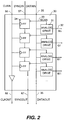
- Display 10 can represent an entire display or a portion thereof.
- Display 10 has an emissive image area that causes light emission.
- the emissive image area that comprises a plurality of light-emitting pixels, e.g. red light-emitting pixels such as 20r, green light-emitting pixels such as 20g, blue light-emitting pixels such as 20b, and white light-emitting pixels such as 20w.
- the light-emitting pixels can be any form of electronic display, e.g. OLED or LCD, and are not limited to the combinations of colors in this embodiment.
- the pixels in the emissive area are arranged in groups of pixels, e.g.
- Display 10 includes a plurality of sequentially arranged pixel drive circuits, e.g. pixel drive circuits 30 and 50, and other pixel drive circuits that can be located above pixel drive circuit 30 or below pixel drive circuit 50.
- the term "sequentially arranged" as used herein means that 1) the pixel drive circuits are so located to form a sequence in space of such drive circuits, e.g. a linear sequence on a support, 2) the pixel drive circuits perform their operations in the same sequence as their spatial location, and 3) all of the pixel drive circuits in a sequence are electrically connected serially in a chain configuration by at least one communication connection. Each pixel drive circuit is thus electrically connected to the next sequential pixel drive circuit.
- the display further includes parallel communication connections for providing a portion of the data to the pixel drive circuits.
- the terms “series”, “serially”, and “parallel” used herein refer to the arrangement of the communication paths to the pixel drive circuits.
- Each pixel drive circuit is electrically connected to a particular group of pixels, e.g. pixel drive circuit 30 is connected (via electrical connections, e.g. 40 ) to the pixels of group of pixels 20 so as to control the light emission from those pixels.
- Pixel drive circuit 30 determines the brightness level of each pixel in group of pixels 20 according to data received, as will be seen.
- Pixel drive circuit 30 can be, for example, a separately fabricated integrated circuit, and will be described further below.
- the data can be represented as either digital data or in the form of analog voltage signals relating to the desired brightness and color of the individual sub-pixels, pixels, or groups of pixels.
- Display 10 further includes an apparatus for controlling the operation of pixel drive circuit 30.
- This control apparatus includes one or more signal communication lines, e.g. data line 25 and control line 55, and a control device, e.g. data source 80, which can be external to display 10, for providing data onto data line 25 and control signals onto control line 55.
- Data source 80 is an example of a control device for providing data for controlling the operation of the pixel drive circuits and their corresponding pixels.
- Data source 80 can be a device known in the art to be useful for controlling displays, such as a processor or an application-specific integrated circuit.
- the first pixel drive circuit is thus electrically connected to the control device and receives data from the control device. The provided data and signals control the operation of the pixel drive circuits.
- Other data and control lines can be connected to the sequentially arranged pixel drive circuits. At least one of the signal communication lines, such as control line 55 and subsequent control lines (e.g. control lines 65 and 75 ), is electrically connected in series with the sequentially arranged pixel drive circuits. Other signal communication lines, e.g. data line 25 and subsequent data lines, are parallel signal communication lines for providing a portion of the data for controlling the operation of each pixel drive circuit.
- the control device provides sequential data on data line 25 for controlling the emission of the pixels of display 10 by providing data first for all the pixels connected to pixel drive circuit 30, then for all the pixels connected to pixel drive circuit 50, and sequentially for each successive pixel drive circuit.
- information is provided to pixel drive circuit 30 by providing a signal on control line 55 to cause pixel drive circuit 30 to respond to its corresponding data on data line 25 to control the operation of group of pixels 20.
- Pixel drive circuit 30 responds to the data and controls the operation of the individual pixels.
- pixel drive circuit 30 provides information to the next sequential pixel drive circuit, e.g. to pixel drive circuit 50 via a signal on control line 65.
- the information causes pixel drive circuit 50 to respond to its corresponding data on data line 35 to control the operation of its group of light-emitting pixels.
- pixel drive circuit 50 When pixel drive circuit 50 is complete, it provides information to the next sequential pixel drive circuit, e.g. via a signal on control line 75, that the corresponding data is available on data line 45. This process is repeated until a predetermined number of pixel drive circuits have caused the desired light emission from the emissive area of display 10.
- the operation of the final pixel drive circuit need be no different from the others, thereby simplifying manufacturing.
- the final pixel drive circuit will act to signal to a successive pixel drive circuit; however, no successive pixel drive circuit will be available to receive the signal.
- the data source will stop sending data, ending the data transmission sequence.
- the data source will then place a signal on the control line to the first pixel drive circuit to indicate that a new sequence of data transmission is beginning.
- Display 10 also includes other lines commonly used in such displays, such as power and ground lines. These have been omitted for clarity of illustration of the salient features of this invention.
- Control lines 55, 65, and 75 are constructed to be non-continuous, that is, a series connection with the pixel drive circuits, such that each pixel drive circuit controls the subsequent control line.
- Data lines 25, 35, 45, and any subsequent lines, can form a continuous line from the top to the bottom of display 10 (parallel connection).
- pixel drive circuit 30 provides information to next sequential pixel drive circuit 50 that causes pixel drive circuit 50 to respond to its corresponding data. It will be understood that other embodiments are possible. In some alternate embodiments, it is not necessary to have both a control line and a data line. In these embodiments, a single discontinuous signal communication line (e.g. data lines 25, 35, etc.) connected in series with the pixel drive circuits will suffice. In one such alternate embodiment, pixel drive circuit 30 responds to the first data it receives, but does not pass data to the next pixel drive circuit 50, until it has finished responding to its data. It then continues to pass data, while counting the incoming data until the data equal to the number of rows has been received.
- a single discontinuous signal communication line e.g. data lines 25, 35, etc.
- pixel drive circuit 30 can set one or more control bits in the data stream to indicate that the data is meant for pixel drive circuit 50.
- This embodiment has the advantage that the external control device can set the control bit(s) to indicate to the first pixel drive circuit in the sequence that it must process the data, thus restarting the data delivery sequence.
- control lines can be utilized prior to commencing display operation.
- the control lines ( 55, etc.) have series connections, while the data lines ( 25, etc.) have parallel connections with the integrated circuits.
- pixel drive circuit 30 includes registers for storing an address. Before display operation-which can be at every power-on for the display, or one time only when the display is manufactured-a signal is placed on control line 55 that pixel drive circuit 30 is to store a sequence identification number indicating its sequence or address in the display. It in turn places a signal on control line 65 that pixel drive circuit 50 is to store an incremented number indicating its sequence, and so forth to the bottom of the display.
- each pixel drive circuit will respond only when its previously stored sequence identification number appears in the data stream.
- the pixel drive circuit itself can determine when to process the data by waiting until an appropriate quantity of data based on its predetermined sequence identification number has been transmitted to lower-numbered pixel drive circuits.
- the embodiment shown in FIG. 1 can be repeated one or more times to continue the sequence shown and increase the length of the display.
- the embodiment can be repeated one or more times in parallel on the same physical display to increase the width of the display.
- Pixel drive circuit 30 can be an integrated circuit that is separately fabricated and later mounted to display 10.
- nominal control line 55 (see Fig. 1 ) actually comprises two lines: clock in 56 and sync in 57; similarly, control line 65 (see Fig.1 ) comprises clock out 66 and sync out 67.
- Clock in 56 and sync in 57 control when data line 25 programs a subpixel driven by the pixel drive circuit.
- the digital portion of the circuit is a shift register comprised of flip flops (FF) 34. Current is supplied to subpixel anode 32 by analog drive circuit 31.
- analog drive circuit 31 is shown in FIG. 3 .
- the voltage signal corresponding to the desired pixel luminance is stored on storage capacitor 38, which regulates the current through drive transistor 36 to control the light emission of the pixel.
- Scan transistor 37 allows the voltage on data line 25 to be stored on storage capacitor 38 when scan signal 33 is enabled.
- the circuitry in pixel drive circuit 30 can optionally include circuits known in the art to compensate for thermal effects and aging of the display.
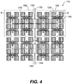
- a pixel drive circuit controls the operation of a larger group of light-emitting pixels, e.g. group of pixels 180.
- the pixel drive circuit comprises a first integrated circuit 130, one or more second integrated circuits in the area of the corresponding group of pixels, e.g. second integrated circuit 160.
- First integrated circuits 130 and 150 and second integrated circuits 160 can be separately fabricated and later mounted to display 110.
- Each second integrated circuit 160 is electrically connected to a first integrated circuit (e.g. 130 ) via electrical connections 170, and to a group of pixels, e.g. group of pixels 120, via electrical connections 140.
- connection 170 is represented as a single line, but it will be understood that connection 170 can represent multiple lines as necessary.
- integrated circuits 130 and 150 are analogous to pixel drive circuits 30 and 50 of display 10, above, in the function of receiving and sending data via data lines 125, 135, and 145.
- first integrated circuits 130 and 150 do not control the pixels directly. Instead, first integrated circuit 130 distributes its data to one or more separately fabricated second integrated circuits, e.g. second integrated circuit 160, which controls the light emission of its corresponding group of light-emitting pixels, e.g. group of pixels 120.
- the first integrated circuits can be considered first-tier or master integrated circuits, while the second integrated circuits can be considered second-tier or slave integrated circuits.
- first integrated circuit 130 can be designed and optimized for high-speed digital data reception, processing, and transmission
- second integrated circuit 160 can be designed and optimized for higher-power pixel control via analog current drive. Since integrated-circuit manufacturers can provide either of these process types separately, but not easily provide both simultaneously, it is an advantage to separate these functions into different integrated circuit chips. That is, first integrated circuit 130 handles the digital information part embodied in flip flops 34 in FIG. 2 , and can be made using a small feature-size process (0.35, 0.18, 0.13 micrometer etc.), with low voltage (5V or 3.3V) digital logic type transistors, while second integrated circuit 160 can include analog drive circuits similar to those of FIG. 2 and can be made using a larger feature-size process (0.5 micrometer, etc.) with high voltage type transistors (15V or 18V type).
- the data lines function for both data distribution (as in display 10 ) and pixel drive circuit control (as the control lines in display 10 ).
- This can be achieved by the use of one or more extra information bits in the data stream, such that both data sequences and command sequences are possible, as described above.
- a command sequence to first integrated circuit 130 via data line 125 from an external controller will cause first integrated circuit 130 to receive data that it distributes to its corresponding second integrated circuits.
- it sends a command sequence to first integrated circuit 150 and passes along the data that first integrated circuit 150 then uses to control the operation of its corresponding pixels.
- separate data and control lines, as in display 10 can be used in this embodiment as well.
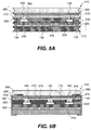
- FIG. 5A is a direct cross-section of display 110 from FIG. 4 along the straight line from data line 125 to data line 145.
- Display 110 can be formed on a substrate 210.
- Substrate 210 is desirably a flexible material, including metal foil, plastic, or combinations of metal and plastic. More convention glass materials can also be employed as the substrate.
- substrate 210 is a metal foil such as aluminum or stainless steel. In such a case, the substrate is opaque to light transmission, and light will therefore be emitted from the side of display 110 opposite to substrate 210.
- insulating layer 220 is placed over it.
- Patterned electrical connections are placed over insulating layer 220.
- the electrical connections can include signal data lines and control lines as described above, e.g. data lines 125, 135, and 145, as well as other electrical connections necessary or useful in electronic displays, such as power and ground lines (although one of these can be performed by substrate 210 if it is a metal foil), timing or handshaking connections, and circuit test lines.
- Patterning of this and other layers described herein can be accomplished by methods well-known to those skilled in the art, including, but not limited to, conventional deposition and photolithography, through-mask (shadow mask) deposition, integral shadow masking as described in U.S. Patent 5,276,380 and EP 0 732 868 , laser ablation, selective chemical vapor deposition, and digital lithography.
- An adhesive 240 is placed over the layer of electrical connections.
- Integrated circuits which have been described above, are mounted on substrate 210 by adhesive 240, and via holes, e.g. via 235, are formed where necessary to for connection to the layer of electrical connections.
- Integrated circuits e.g. first integrated circuits 130 and 150, can be fabricated as conventional integrated circuits together in quantity on a wafer as is common in the art and placed separately onto adhesive 240 by methods that have been described by Nuzzo et al. in US 2007/0032089 A1 , WO 2005/122285 A3 , and WO 2006/130721 A2 . Other methods of attaching integrated circuits to a display substrate are described by Matsumura et al.
- Patterned insulating layer 260 provides insulation for the electrical connection layer except at desired locations, e.g. via 235.
- Patterned wire layer 265 then provides electrical connections between the integrated circuits and the electrical connection layer.
- an insulating layer 270 Over this is an insulating layer 270, which will be shown to be a patterned insulating layer, and OLED layers 275.
- FIG. 5B is a schematic cross-sectional view of display 110 of FIG. 4 from X to X'. Specifically, the cross-section in FIG. 5B is from X to a colored pixel, to corresponding connection 140, to corresponding second integrated circuit 160, to corresponding connection 170, to first integrated circuit 130, and via corresponding structures to X'.
- First integrated circuit 130 and second integrated circuit 160 are mounted on substrate 210 by adhesive 240.
- Patterned wire layer 265, as described above, also includes previously described connections 170 between first and second integrated circuits 130 and 160, respectively, and connections 140 between second integrated circuits 160 and the light-emitting pixels 245.
- the patterned wire layer can thus serve as the lower electrode (e.g.
- OLED layers 275 can include layers commonly used in such devices, e.g. hole-transporting layers, electron-transporting layers, light-emitting layers, and other layers well-known in the art.
- the pixels in this embodiment comprise OLED devices.
- an upper electrode which in this embodiment is cathode 280.
- cathode 280 wraps around the edges of display 110, so that the substrate electrically contacts the electrode and can conduct electricity to or from the light-emitting pixels.
- the display is top-emitting, such that light is emitted from the side opposite substrate 210, that is, through cathode 280 and transparent cover 290.
- a full color device can be achieved using a common broadband layer (e.g. a white OLED layer) and color filters 285.
- the color filters can be preprinted onto a transparent cover 290, which can comprise glass or plastic.
- the color filters can be formed on top of cathode 280.
- transparent cover 290 can be attached in some embodiments, or can be left off if the display is to be placed against a display support as described below.
- the color filters are formed on a display support, which will be described below, to which one or more display elements can be aligned and affixed.
- Full color OLED devices can also be formed by using a shadow mask for depositing red-, green-, and blue-emitting OLED materials selectively over different pixels.
- the display can be covered with a transparent cover 290, but color filters are not needed.
- transparent cover 290 can be replaced with a thin-film encapsulation layer formed over the emissive display.
- FIG. 5B is simplified for clarity of illustration.
- Display 110 will typically have many more pixels and color filters across a cross-section.
- Tiled display 310 includes a plurality of display tiles 330, which include first edges 340 that are parallel to each other, and second edge 350 perpendicular to first edges 340. First edges 340 are longer than second edges 350.
- Each display tile 330 can be constructed as described above for displays 10 and 110; that is, each display tile 330 includes a substrate as described above, a plurality of light-emitting pixels formed on the substrate and arranged in groups of pixels as described above, a plurality of sequentially arranged pixel drive circuits as described above, and one or more signal communication lines as described above.
- the signal communication lines, and thus the sequence of pixel drive circuits, are arranged parallel to first edges 340.
- the sequentially arranged pixel drive circuits can include a series of integrated circuits, as shown in FIG. 1 , mounted on the substrate.
- the sequentially arranged pixel drive circuits can include a series of first integrated circuits mounted on the substrate, each of which is electrically connected to one or more second integrated circuits mounted on the substrate, as shown in FIG. 4 .
- the sequentially arranged pixel drive circuits operate as described above.
- Each pixel drive circuit of a display tile controls the light emission of its corresponding group of pixels, and provides information to the next sequential pixel drive circuit on display tile 340 to cause the next sequential pixel drive circuit to respond to its corresponding data to control the operation of its corresponding group of light-emitting pixels.
- Display tiles 330 are aligned on display support 320 along first parallel edges 340 so that they provide the tiled display's emissive image area, which comprises the combined emissive areas of all the display tiles.
- Display tiles 330 can be aligned and affixed with the emitting-side face to display support 320 using an adhesive.
- the display support 320 is light-transmissive for viewing the emission through the support.
- Transparent glass or plastic can be employed and display support 320 can be rigid or flexible.
- display support 320 can be preprinted with color filters and alignment marks, eliminating the need for a separate color filter substrate.
- Display tiles 330 are then lined-up with the alignment marks so that the light emitting areas are aligned with the color filters, and display tiles 330 are affixed to display support 320 with adhesive. If encapsulation is required and the encapsulation of the individual display tiles (e.g. by transparent cover 290 ) is not sufficient for the required display lifetime, tiled display 310 can be further sealed by covering the non-emitting side of the display tiles with a water and oxygen impermeable cover such as glass or metal.
- the individual display tiles 330 can extend beyond the edge of display support 320, as shown, or can be terminated inside the area of the support.
- Tiled display 310 further includes data source 360, which is separate from display tiles 330.
- Data source 360 is an example of a control device for providing data for controlling the operation of the pixel drive circuits and their corresponding pixels.
- Data source 360 can be part of display support 320 or can be a separate entity.
- Data source 360 receives image information 370, e.g. pixel intensity, and produces the data to control the light emission from the pixels of each display tile 330 by providing data onto the signal communication lines as described above.
- the signal communication lines of display tiles 330 are connected through second edge 350 to data source 360 by connection 380.
- connection 380 represents one or more lines between data source 360 and display tiles 330, wherein such lines can include data lines, control lines, power and ground lines, handshaking lines, data readout lines, or other lines necessary for display control.
- Connections 380 can be attached to one or both second edges 350; however, connection at a single second edge is desirable to allow lower-cost driving methods using a single data source 360.
- Data source 360 can be a device known in the art to be useful for controlling displays, such as a processor or an application-specific integrated circuit.
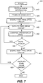
- FIG. 7 a block diagram of a method of using a display of this invention.
- image information 370 is received by data source 360 (Step 410 ), and data source 360 produces data (Step 420 ) that will be used to drive the pixel drive circuits and pixels of the display.
- Data source 360 provides information to the first pixel drive circuit (Step 430 ), e.g. by providing a signal on control line 55 to first pixel drive circuit 30, to begin control of its corresponding group of pixels.
- Data is then provided to the pixel drive circuit (Step 440 ), e.g.
- Step 450 the pixel drive circuit uses the data to control pixels in its corresponding group of pixels (Step 450 ). If there are more pixels in the corresponding group (Step 460 ), Steps 440 and 450 are repeated as necessary.
- pixel drive circuit 30 provides information to the next sequential pixel drive circuit, e.g. via a signal over control line 65 (Step 470 ), for the next pixel drive circuit to respond to its corresponding data to control the operation of its group of light-emitting pixels. If there is a next sequential pixel drive circuit (Step 480 ), Steps 440 to 470 are repeated as necessary.
- Step 480 If there is no further pixel drive circuit (Step 480 ), the process ends.
- the last sequential pixel drive circuit will therefore include the ability to signal a further pixel drive circuit.
- data source 360 will not provide any further data. Instead, data source 360 will restart process 400 with new information (Step 410 ), produce new image data (Step 420 ), and signal the first pixel drive circuit to begin accepting data again (Step 430 ).
- a tiled display e.g. tiled display 310, the above process is used for each display tile.
- the last pixel drive circuit can signal the first pixel drive circuit to start responding to data again.
- this embodiment would require an extra line that runs a predetermined length in each display tile, and is thus a less-desirable embodiment.
Landscapes
- Engineering & Computer Science (AREA)
- Theoretical Computer Science (AREA)
- Physics & Mathematics (AREA)
- General Physics & Mathematics (AREA)
- Computer Hardware Design (AREA)
- Microelectronics & Electronic Packaging (AREA)
- General Engineering & Computer Science (AREA)
- Chemical & Material Sciences (AREA)
- Crystallography & Structural Chemistry (AREA)
- Human Computer Interaction (AREA)
- Electroluminescent Light Sources (AREA)
- Devices For Indicating Variable Information By Combining Individual Elements (AREA)
- Control Of Indicators Other Than Cathode Ray Tubes (AREA)
Applications Claiming Priority (2)
| Application Number | Priority Date | Filing Date | Title |
|---|---|---|---|
| US12/164,295 US8179336B2 (en) | 2008-06-30 | 2008-06-30 | Tiled electronic display |
| PCT/US2009/003617 WO2010008441A1 (en) | 2008-06-30 | 2009-06-17 | Tiled electronic display |
Publications (2)
| Publication Number | Publication Date |
|---|---|
| EP2304541A1 EP2304541A1 (en) | 2011-04-06 |
| EP2304541B1 true EP2304541B1 (en) | 2018-07-18 |
Family
ID=41056702
Family Applications (1)
| Application Number | Title | Priority Date | Filing Date |
|---|---|---|---|
| EP09788801.0A Active EP2304541B1 (en) | 2008-06-30 | 2009-06-17 | Tiled electronic display |
Country Status (6)
| Country | Link |
|---|---|
| US (1) | US8179336B2 (https=) |
| EP (1) | EP2304541B1 (https=) |
| JP (1) | JP5236805B2 (https=) |
| KR (1) | KR101267899B1 (https=) |
| CN (1) | CN102077167B (https=) |
| WO (1) | WO2010008441A1 (https=) |
Families Citing this family (34)
| Publication number | Priority date | Publication date | Assignee | Title |
|---|---|---|---|---|
| US8619008B2 (en) * | 2009-02-13 | 2013-12-31 | Global Oled Technology Llc | Dividing pixels between chiplets in display device |
| US8896505B2 (en) | 2009-06-12 | 2014-11-25 | Global Oled Technology Llc | Display with pixel arrangement |
| CN102592516B (zh) * | 2012-02-29 | 2013-12-25 | 信利半导体有限公司 | 一种大尺寸显示屏 |
| US10002561B1 (en) | 2012-12-12 | 2018-06-19 | Christopher Ralph Tridico | Perceptually configured array of addressable electromagnetic emitter elements |
| TW201430809A (zh) * | 2013-01-11 | 2014-08-01 | Sony Corp | 顯示面板、像素晶片及電子機器 |
| US20150022754A1 (en) * | 2013-07-19 | 2015-01-22 | Google Inc. | Configurations for tileable display apparatus with multiple pixel arrays |
| KR102161644B1 (ko) * | 2014-08-20 | 2020-10-06 | 삼성디스플레이 주식회사 | 스트레쳐블 표시 패널 및 이를 포함하는 표시 장치 |
| US11125904B2 (en) | 2014-12-12 | 2021-09-21 | Lingacom Ltd. | Large scale gas electron multiplier with sealable opening |
| US10191180B2 (en) * | 2014-12-12 | 2019-01-29 | Lingacom Ltd. | Large scale gas electron multiplier and detection method |
| KR102606673B1 (ko) * | 2016-10-21 | 2023-11-28 | 삼성디스플레이 주식회사 | 표시 패널, 입체 영상 표시 패널 및 표시 장치 |
| WO2019058307A1 (en) * | 2017-09-20 | 2019-03-28 | Imax Theatres International Limited | LIGHT EMITTING DISPLAY WITH PAVERS AND DATA PROCESSING |
| NL2019867B1 (en) * | 2017-11-08 | 2019-05-15 | Eldolab Holding Bv | method of operating a distributed light source and distributed light source. |
| US11263963B2 (en) | 2018-05-09 | 2022-03-01 | Apple Inc. | Local passive matrix display |
| US10854129B2 (en) | 2018-06-18 | 2020-12-01 | Apple Inc. | Hybrid architecture for zero border display |
| CN110782804B (zh) * | 2018-07-30 | 2021-11-12 | 上海雷舞照明技术有限公司 | 显示装置及亮化系统 |
| KR102577240B1 (ko) | 2018-11-21 | 2023-09-12 | 삼성디스플레이 주식회사 | 타일드 표시 장치 |
| CN111508935B (zh) * | 2019-01-31 | 2022-03-15 | 群创光电股份有限公司 | 拼接显示装置 |
| CN109741683B (zh) * | 2019-03-22 | 2021-04-27 | 京东方科技集团股份有限公司 | 显示屏和拼接屏 |
| JP2021028679A (ja) * | 2019-08-09 | 2021-02-25 | 株式会社ブイ・テクノロジー | 発光表示装置および発光表示装置の画素回路チップ |
| TWI719721B (zh) * | 2019-11-20 | 2021-02-21 | 友達光電股份有限公司 | 拼接顯示器及其製造方法 |
| WO2021103014A1 (zh) | 2019-11-29 | 2021-06-03 | 京东方科技集团股份有限公司 | 阵列基板、显示面板、拼接显示面板及显示驱动方法 |
| CN115428146A (zh) * | 2020-04-21 | 2022-12-02 | 赫二虚拟现实控股公司 | 包含多个像素和子像素的表面安装器件 |
| CN111627382B (zh) * | 2020-06-30 | 2022-02-15 | 上海天马微电子有限公司 | 拼接显示屏及显示装置 |
| KR20220049082A (ko) | 2020-10-13 | 2022-04-21 | 삼성디스플레이 주식회사 | 타일 조립형 표시 장치, 그 제조를 위한 표시 패널 정렬 장치 및 제조 방법 |
| KR102740142B1 (ko) * | 2020-10-21 | 2024-12-06 | 엘지디스플레이 주식회사 | 전계발광 표시장치 |
| KR102832919B1 (ko) * | 2021-03-16 | 2025-07-11 | 삼성디스플레이 주식회사 | 표시 장치와 그를 포함하는 타일형 표시 장치 |
| CN113410259B (zh) * | 2021-06-09 | 2022-05-20 | 深圳蓝普视讯科技有限公司 | 倒装芯片空间像素排布结构和显示面板装置 |
| CN115631710B (zh) * | 2021-07-16 | 2025-03-21 | 群创光电股份有限公司 | 显示面板 |
| WO2023019598A1 (zh) * | 2021-08-20 | 2023-02-23 | 京东方科技集团股份有限公司 | 显示装置、显示面板及其驱动方法 |
| CN115909890A (zh) * | 2021-08-26 | 2023-04-04 | 中兴通讯股份有限公司 | 一种显示面板及显示装置 |
| TWI798845B (zh) * | 2021-09-28 | 2023-04-11 | 友達光電股份有限公司 | 發光面板 |
| CN115273726B (zh) * | 2022-09-01 | 2025-08-29 | 合肥鑫晟光电科技有限公司 | 显示基板、显示面板及显示装置 |
| CN120476440A (zh) | 2022-11-09 | 2025-08-12 | 三星电子株式会社 | 包括多个驱动器ic的显示设备、模块化显示设备及其控制方法 |
| WO2025225273A1 (ja) * | 2024-04-23 | 2025-10-30 | 株式会社Magnolia White | 表示装置 |
Citations (3)
| Publication number | Priority date | Publication date | Assignee | Title |
|---|---|---|---|---|
| US5422885A (en) * | 1992-06-01 | 1995-06-06 | Motorola, Inc. | Contention free local area network |
| US5914957A (en) * | 1996-12-19 | 1999-06-22 | Otis Elevator Company | Automatic node configuration with identical nodes |
| US6670882B1 (en) * | 1999-07-28 | 2003-12-30 | Cisco Technology, Inc. | Multi drop stack bus detector method and apparatus |
Family Cites Families (24)
| Publication number | Priority date | Publication date | Assignee | Title |
|---|---|---|---|---|
| DE3910418A1 (de) | 1989-03-31 | 1990-10-04 | Licentia Gmbh | Anzeigevorrichtung |
| US5276380A (en) | 1991-12-30 | 1994-01-04 | Eastman Kodak Company | Organic electroluminescent image display device |
| FR2701586B1 (fr) | 1993-02-12 | 1995-03-24 | Souriau Diagnostic Electron | Dispositif d'affichage à cristaux liquides comprenant un réseau de points images. |
| JP3813217B2 (ja) | 1995-03-13 | 2006-08-23 | パイオニア株式会社 | 有機エレクトロルミネッセンスディスプレイパネルの製造方法 |
| US5644327A (en) | 1995-06-07 | 1997-07-01 | David Sarnoff Research Center, Inc. | Tessellated electroluminescent display having a multilayer ceramic substrate |
| US5889568A (en) | 1995-12-12 | 1999-03-30 | Rainbow Displays Inc. | Tiled flat panel displays |
| US5661531A (en) | 1996-01-29 | 1997-08-26 | Rainbow Displays Inc. | Tiled, flat-panel display having invisible seams |
| US6274987B1 (en) * | 1996-05-08 | 2001-08-14 | Magnetek, Inc. | Power sensing lamp protection circuit for ballasts driving gas discharge lamps |
| US5903328A (en) | 1997-06-16 | 1999-05-11 | Rainbow Displays, Inc. | Tiled flat-panel display with tile edges cut at an angle and tiles vertically shifted |
| US6259838B1 (en) | 1998-10-16 | 2001-07-10 | Sarnoff Corporation | Linearly-addressed light-emitting fiber, and flat panel display employing same |
| US6274978B1 (en) | 1999-02-23 | 2001-08-14 | Sarnoff Corporation | Fiber-based flat panel display |
| DE19950839A1 (de) | 1999-10-21 | 2001-05-23 | Fraunhofer Ges Forschung | Vorrichtung zur Ansteuerung der Anzeigeelemente eines Anzeigeelementenarrays und Verfahren zur Herstellung derselben |
| US6614171B2 (en) | 2001-01-10 | 2003-09-02 | Eastman Kodak Company | Light-producing display having spaced apart tiles |
| JP2002311881A (ja) | 2001-04-19 | 2002-10-25 | Nichia Chem Ind Ltd | 画像表示装置 |
| US6999045B2 (en) * | 2002-07-10 | 2006-02-14 | Eastman Kodak Company | Electronic system for tiled displays |
| KR20050075280A (ko) | 2002-11-19 | 2005-07-20 | 가부시키가이샤 이시카와 세이사쿠쇼 | 화소제어 소자의 선택 전사 방법, 화소제어 소자의 선택전사 방법에 사용되는 화소제어 소자의 실장 장치,화소제어 소자 전사후의 배선 형성 방법, 및, 평면디스플레이 기판 |
| EP1814100A3 (en) | 2003-05-23 | 2008-03-05 | Barco, naamloze vennootschap. | Method for displaying images on a large-screen organic light-emitting diode display, and display used therefore |
| EP1513060A1 (en) | 2003-09-08 | 2005-03-09 | Barco N.V. | Large-area display system, modular unit used therein and method of operating the display |
| EP1548573A1 (en) | 2003-12-23 | 2005-06-29 | Barco N.V. | Hierarchical control system for a tiled large-screen emissive display |
| US7799699B2 (en) | 2004-06-04 | 2010-09-21 | The Board Of Trustees Of The University Of Illinois | Printable semiconductor structures and related methods of making and assembling |
| KR101260981B1 (ko) | 2004-06-04 | 2013-05-10 | 더 보오드 오브 트러스티스 오브 더 유니버시티 오브 일리노이즈 | 인쇄가능한 반도체소자들의 제조 및 조립방법과 장치 |
| US20060044215A1 (en) | 2004-08-24 | 2006-03-02 | Brody Thomas P | Scalable tiled display assembly for forming a large-area flat-panel display by using modular display tiles |
| EP1915774B1 (en) | 2005-06-02 | 2015-05-20 | The Board Of Trustees Of The University Of Illinois | Printable semiconductor structures and related methods of making and assembling |
| US8041310B2 (en) * | 2007-10-01 | 2011-10-18 | Telefonaktiebolaget Lm Ericsson (Publ) | Apparatus and methods for frequency control in a multi-output frequency synthesizer |
-
2008
- 2008-06-30 US US12/164,295 patent/US8179336B2/en active Active
-
2009
- 2009-06-17 WO PCT/US2009/003617 patent/WO2010008441A1/en not_active Ceased
- 2009-06-17 KR KR1020117002256A patent/KR101267899B1/ko active Active
- 2009-06-17 CN CN200980125384.7A patent/CN102077167B/zh active Active
- 2009-06-17 EP EP09788801.0A patent/EP2304541B1/en active Active
- 2009-06-17 JP JP2011516274A patent/JP5236805B2/ja active Active
Patent Citations (3)
| Publication number | Priority date | Publication date | Assignee | Title |
|---|---|---|---|---|
| US5422885A (en) * | 1992-06-01 | 1995-06-06 | Motorola, Inc. | Contention free local area network |
| US5914957A (en) * | 1996-12-19 | 1999-06-22 | Otis Elevator Company | Automatic node configuration with identical nodes |
| US6670882B1 (en) * | 1999-07-28 | 2003-12-30 | Cisco Technology, Inc. | Multi drop stack bus detector method and apparatus |
Also Published As
| Publication number | Publication date |
|---|---|
| US20090322649A1 (en) | 2009-12-31 |
| JP2011527023A (ja) | 2011-10-20 |
| US8179336B2 (en) | 2012-05-15 |
| JP5236805B2 (ja) | 2013-07-17 |
| WO2010008441A1 (en) | 2010-01-21 |
| KR20110028527A (ko) | 2011-03-18 |
| CN102077167A (zh) | 2011-05-25 |
| KR101267899B1 (ko) | 2013-05-28 |
| CN102077167B (zh) | 2014-01-29 |
| EP2304541A1 (en) | 2011-04-06 |
Similar Documents
| Publication | Publication Date | Title |
|---|---|---|
| EP2304541B1 (en) | Tiled electronic display | |
| EP2446430B1 (en) | Passive-matrix chiplet drivers for displays | |
| US9492993B2 (en) | Chiplet display with multiple passive-matrix controllers | |
| US6888304B2 (en) | Display module | |
| US6281634B1 (en) | Color electroluminescence display device | |
| US8497821B2 (en) | Chiplet display device with serial control | |
| US8619008B2 (en) | Dividing pixels between chiplets in display device | |
| EP2399253B1 (en) | Display device with chiplet drivers | |
| US8259095B2 (en) | Optically testing chiplets in display device | |
| US20040130514A1 (en) | Color electroluminescence display device | |
| CN108807466A (zh) | 显示装置 | |
| KR100556540B1 (ko) | 전기 광학 장치, 매트릭스 기판, 및 전자 기기 | |
| US20110043541A1 (en) | Fault detection in electroluminescent displays | |
| CN111430433B (zh) | 显示面板及显示装置 | |
| KR102293456B1 (ko) | 표시 패널 | |
| US8247966B2 (en) | Organic light emitting device | |
| US20060114190A1 (en) | Active matrix organic electro-luminescence device array | |
| WO2007064115A1 (en) | Display cosisting of socket type oleds and method for manufacturing of the same | |
| CN116111025A (zh) | 一种显示面板及显示装置 |
Legal Events
| Date | Code | Title | Description |
|---|---|---|---|
| PUAI | Public reference made under article 153(3) epc to a published international application that has entered the european phase |
Free format text: ORIGINAL CODE: 0009012 |
|
| 17P | Request for examination filed |
Effective date: 20110120 |
|
| AK | Designated contracting states |
Kind code of ref document: A1 Designated state(s): AT BE BG CH CY CZ DE DK EE ES FI FR GB GR HR HU IE IS IT LI LT LU LV MC MK MT NL NO PL PT RO SE SI SK TR |
|
| AX | Request for extension of the european patent |
Extension state: AL BA RS |
|
| DAX | Request for extension of the european patent (deleted) | ||
| RAP1 | Party data changed (applicant data changed or rights of an application transferred) |
Owner name: GLOBAL OLED TECHNOLOGY LLC |
|
| 17Q | First examination report despatched |
Effective date: 20111202 |
|
| REG | Reference to a national code |
Ref country code: DE Ref legal event code: R079 Ref document number: 602009053354 Country of ref document: DE Free format text: PREVIOUS MAIN CLASS: G06F0003140000 Ipc: G09G0003323300 |
|
| GRAP | Despatch of communication of intention to grant a patent |
Free format text: ORIGINAL CODE: EPIDOSNIGR1 |
|
| STAA | Information on the status of an ep patent application or granted ep patent |
Free format text: STATUS: GRANT OF PATENT IS INTENDED |
|
| RIC1 | Information provided on ipc code assigned before grant |
Ipc: G09G 3/3233 20160101AFI20180124BHEP Ipc: G09G 3/20 20060101ALI20180124BHEP |
|
| INTG | Intention to grant announced |
Effective date: 20180212 |
|
| GRAS | Grant fee paid |
Free format text: ORIGINAL CODE: EPIDOSNIGR3 |
|
| RAP1 | Party data changed (applicant data changed or rights of an application transferred) |
Owner name: GLOBAL OLED TECHNOLOGY LLC |
|
| GRAA | (expected) grant |
Free format text: ORIGINAL CODE: 0009210 |
|
| STAA | Information on the status of an ep patent application or granted ep patent |
Free format text: STATUS: THE PATENT HAS BEEN GRANTED |
|
| AK | Designated contracting states |
Kind code of ref document: B1 Designated state(s): AT BE BG CH CY CZ DE DK EE ES FI FR GB GR HR HU IE IS IT LI LT LU LV MC MK MT NL NO PL PT RO SE SI SK TR |
|
| REG | Reference to a national code |
Ref country code: GB Ref legal event code: FG4D |
|
| REG | Reference to a national code |
Ref country code: CH Ref legal event code: EP |
|
| REG | Reference to a national code |
Ref country code: IE Ref legal event code: FG4D |
|
| REG | Reference to a national code |
Ref country code: DE Ref legal event code: R096 Ref document number: 602009053354 Country of ref document: DE |
|
| REG | Reference to a national code |
Ref country code: AT Ref legal event code: REF Ref document number: 1020197 Country of ref document: AT Kind code of ref document: T Effective date: 20180815 |
|
| REG | Reference to a national code |
Ref country code: NL Ref legal event code: FP |
|
| REG | Reference to a national code |
Ref country code: LT Ref legal event code: MG4D |
|
| REG | Reference to a national code |
Ref country code: AT Ref legal event code: MK05 Ref document number: 1020197 Country of ref document: AT Kind code of ref document: T Effective date: 20180718 |
|
| PG25 | Lapsed in a contracting state [announced via postgrant information from national office to epo] |
Ref country code: PL Free format text: LAPSE BECAUSE OF FAILURE TO SUBMIT A TRANSLATION OF THE DESCRIPTION OR TO PAY THE FEE WITHIN THE PRESCRIBED TIME-LIMIT Effective date: 20180718 Ref country code: LT Free format text: LAPSE BECAUSE OF FAILURE TO SUBMIT A TRANSLATION OF THE DESCRIPTION OR TO PAY THE FEE WITHIN THE PRESCRIBED TIME-LIMIT Effective date: 20180718 Ref country code: IS Free format text: LAPSE BECAUSE OF FAILURE TO SUBMIT A TRANSLATION OF THE DESCRIPTION OR TO PAY THE FEE WITHIN THE PRESCRIBED TIME-LIMIT Effective date: 20181118 Ref country code: AT Free format text: LAPSE BECAUSE OF FAILURE TO SUBMIT A TRANSLATION OF THE DESCRIPTION OR TO PAY THE FEE WITHIN THE PRESCRIBED TIME-LIMIT Effective date: 20180718 Ref country code: BG Free format text: LAPSE BECAUSE OF FAILURE TO SUBMIT A TRANSLATION OF THE DESCRIPTION OR TO PAY THE FEE WITHIN THE PRESCRIBED TIME-LIMIT Effective date: 20181018 Ref country code: NO Free format text: LAPSE BECAUSE OF FAILURE TO SUBMIT A TRANSLATION OF THE DESCRIPTION OR TO PAY THE FEE WITHIN THE PRESCRIBED TIME-LIMIT Effective date: 20181018 Ref country code: GR Free format text: LAPSE BECAUSE OF FAILURE TO SUBMIT A TRANSLATION OF THE DESCRIPTION OR TO PAY THE FEE WITHIN THE PRESCRIBED TIME-LIMIT Effective date: 20181019 Ref country code: SE Free format text: LAPSE BECAUSE OF FAILURE TO SUBMIT A TRANSLATION OF THE DESCRIPTION OR TO PAY THE FEE WITHIN THE PRESCRIBED TIME-LIMIT Effective date: 20180718 Ref country code: FI Free format text: LAPSE BECAUSE OF FAILURE TO SUBMIT A TRANSLATION OF THE DESCRIPTION OR TO PAY THE FEE WITHIN THE PRESCRIBED TIME-LIMIT Effective date: 20180718 |
|
| REG | Reference to a national code |
Ref country code: CH Ref legal event code: PK Free format text: BERICHTIGUNGEN |
|
| RIC2 | Information provided on ipc code assigned after grant |
Ipc: G09G 3/20 20060101ALI20180124BHEP Ipc: G09G 3/3233 20160101AFI20180124BHEP |
|
| PG25 | Lapsed in a contracting state [announced via postgrant information from national office to epo] |
Ref country code: HR Free format text: LAPSE BECAUSE OF FAILURE TO SUBMIT A TRANSLATION OF THE DESCRIPTION OR TO PAY THE FEE WITHIN THE PRESCRIBED TIME-LIMIT Effective date: 20180718 Ref country code: ES Free format text: LAPSE BECAUSE OF FAILURE TO SUBMIT A TRANSLATION OF THE DESCRIPTION OR TO PAY THE FEE WITHIN THE PRESCRIBED TIME-LIMIT Effective date: 20180718 Ref country code: LV Free format text: LAPSE BECAUSE OF FAILURE TO SUBMIT A TRANSLATION OF THE DESCRIPTION OR TO PAY THE FEE WITHIN THE PRESCRIBED TIME-LIMIT Effective date: 20180718 |
|
| REG | Reference to a national code |
Ref country code: DE Ref legal event code: R097 Ref document number: 602009053354 Country of ref document: DE |
|
| PG25 | Lapsed in a contracting state [announced via postgrant information from national office to epo] |
Ref country code: RO Free format text: LAPSE BECAUSE OF FAILURE TO SUBMIT A TRANSLATION OF THE DESCRIPTION OR TO PAY THE FEE WITHIN THE PRESCRIBED TIME-LIMIT Effective date: 20180718 Ref country code: CZ Free format text: LAPSE BECAUSE OF FAILURE TO SUBMIT A TRANSLATION OF THE DESCRIPTION OR TO PAY THE FEE WITHIN THE PRESCRIBED TIME-LIMIT Effective date: 20180718 Ref country code: IT Free format text: LAPSE BECAUSE OF FAILURE TO SUBMIT A TRANSLATION OF THE DESCRIPTION OR TO PAY THE FEE WITHIN THE PRESCRIBED TIME-LIMIT Effective date: 20180718 Ref country code: EE Free format text: LAPSE BECAUSE OF FAILURE TO SUBMIT A TRANSLATION OF THE DESCRIPTION OR TO PAY THE FEE WITHIN THE PRESCRIBED TIME-LIMIT Effective date: 20180718 |
|
| PLBE | No opposition filed within time limit |
Free format text: ORIGINAL CODE: 0009261 |
|
| STAA | Information on the status of an ep patent application or granted ep patent |
Free format text: STATUS: NO OPPOSITION FILED WITHIN TIME LIMIT |
|
| PG25 | Lapsed in a contracting state [announced via postgrant information from national office to epo] |
Ref country code: SK Free format text: LAPSE BECAUSE OF FAILURE TO SUBMIT A TRANSLATION OF THE DESCRIPTION OR TO PAY THE FEE WITHIN THE PRESCRIBED TIME-LIMIT Effective date: 20180718 Ref country code: DK Free format text: LAPSE BECAUSE OF FAILURE TO SUBMIT A TRANSLATION OF THE DESCRIPTION OR TO PAY THE FEE WITHIN THE PRESCRIBED TIME-LIMIT Effective date: 20180718 |
|
| 26N | No opposition filed |
Effective date: 20190423 |
|
| PG25 | Lapsed in a contracting state [announced via postgrant information from national office to epo] |
Ref country code: SI Free format text: LAPSE BECAUSE OF FAILURE TO SUBMIT A TRANSLATION OF THE DESCRIPTION OR TO PAY THE FEE WITHIN THE PRESCRIBED TIME-LIMIT Effective date: 20180718 |
|
| PG25 | Lapsed in a contracting state [announced via postgrant information from national office to epo] |
Ref country code: MC Free format text: LAPSE BECAUSE OF FAILURE TO SUBMIT A TRANSLATION OF THE DESCRIPTION OR TO PAY THE FEE WITHIN THE PRESCRIBED TIME-LIMIT Effective date: 20180718 |
|
| REG | Reference to a national code |
Ref country code: CH Ref legal event code: PL |
|
| REG | Reference to a national code |
Ref country code: BE Ref legal event code: MM Effective date: 20190630 |
|
| PG25 | Lapsed in a contracting state [announced via postgrant information from national office to epo] |
Ref country code: TR Free format text: LAPSE BECAUSE OF FAILURE TO SUBMIT A TRANSLATION OF THE DESCRIPTION OR TO PAY THE FEE WITHIN THE PRESCRIBED TIME-LIMIT Effective date: 20180718 |
|
| PG25 | Lapsed in a contracting state [announced via postgrant information from national office to epo] |
Ref country code: IE Free format text: LAPSE BECAUSE OF NON-PAYMENT OF DUE FEES Effective date: 20190617 |
|
| PG25 | Lapsed in a contracting state [announced via postgrant information from national office to epo] |
Ref country code: CH Free format text: LAPSE BECAUSE OF NON-PAYMENT OF DUE FEES Effective date: 20190630 Ref country code: LU Free format text: LAPSE BECAUSE OF NON-PAYMENT OF DUE FEES Effective date: 20190617 Ref country code: LI Free format text: LAPSE BECAUSE OF NON-PAYMENT OF DUE FEES Effective date: 20190630 Ref country code: BE Free format text: LAPSE BECAUSE OF NON-PAYMENT OF DUE FEES Effective date: 20190630 |
|
| PG25 | Lapsed in a contracting state [announced via postgrant information from national office to epo] |
Ref country code: PT Free format text: LAPSE BECAUSE OF FAILURE TO SUBMIT A TRANSLATION OF THE DESCRIPTION OR TO PAY THE FEE WITHIN THE PRESCRIBED TIME-LIMIT Effective date: 20181118 |
|
| PG25 | Lapsed in a contracting state [announced via postgrant information from national office to epo] |
Ref country code: CY Free format text: LAPSE BECAUSE OF FAILURE TO SUBMIT A TRANSLATION OF THE DESCRIPTION OR TO PAY THE FEE WITHIN THE PRESCRIBED TIME-LIMIT Effective date: 20180718 |
|
| PG25 | Lapsed in a contracting state [announced via postgrant information from national office to epo] |
Ref country code: MT Free format text: LAPSE BECAUSE OF FAILURE TO SUBMIT A TRANSLATION OF THE DESCRIPTION OR TO PAY THE FEE WITHIN THE PRESCRIBED TIME-LIMIT Effective date: 20180718 Ref country code: HU Free format text: LAPSE BECAUSE OF FAILURE TO SUBMIT A TRANSLATION OF THE DESCRIPTION OR TO PAY THE FEE WITHIN THE PRESCRIBED TIME-LIMIT; INVALID AB INITIO Effective date: 20090617 |
|
| PG25 | Lapsed in a contracting state [announced via postgrant information from national office to epo] |
Ref country code: MK Free format text: LAPSE BECAUSE OF FAILURE TO SUBMIT A TRANSLATION OF THE DESCRIPTION OR TO PAY THE FEE WITHIN THE PRESCRIBED TIME-LIMIT Effective date: 20180718 |
|
| PGFP | Annual fee paid to national office [announced via postgrant information from national office to epo] |
Ref country code: DE Payment date: 20250618 Year of fee payment: 17 |
|
| PGFP | Annual fee paid to national office [announced via postgrant information from national office to epo] |
Ref country code: GB Payment date: 20250618 Year of fee payment: 17 |
|
| PGFP | Annual fee paid to national office [announced via postgrant information from national office to epo] |
Ref country code: NL Payment date: 20250618 Year of fee payment: 17 |
|
| PGFP | Annual fee paid to national office [announced via postgrant information from national office to epo] |
Ref country code: FR Payment date: 20250624 Year of fee payment: 17 |