EP2299300B1 - Light guide, light source apparatus, and reading apparatus - Google Patents
Light guide, light source apparatus, and reading apparatus Download PDFInfo
- Publication number
- EP2299300B1 EP2299300B1 EP10008195.9A EP10008195A EP2299300B1 EP 2299300 B1 EP2299300 B1 EP 2299300B1 EP 10008195 A EP10008195 A EP 10008195A EP 2299300 B1 EP2299300 B1 EP 2299300B1
- Authority
- EP
- European Patent Office
- Prior art keywords
- light
- light guide
- lenses
- emitting
- reflecting surface
- Prior art date
- Legal status (The legal status is an assumption and is not a legal conclusion. Google has not performed a legal analysis and makes no representation as to the accuracy of the status listed.)
- Not-in-force
Links
Images


Classifications
-
- G—PHYSICS
- G02—OPTICS
- G02B—OPTICAL ELEMENTS, SYSTEMS OR APPARATUS
- G02B6/00—Light guides; Structural details of arrangements comprising light guides and other optical elements, e.g. couplings
- G02B6/0001—Light guides; Structural details of arrangements comprising light guides and other optical elements, e.g. couplings specially adapted for lighting devices or systems
- G02B6/0011—Light guides; Structural details of arrangements comprising light guides and other optical elements, e.g. couplings specially adapted for lighting devices or systems the light guides being planar or of plate-like form
- G02B6/0033—Means for improving the coupling-out of light from the light guide
- G02B6/0035—Means for improving the coupling-out of light from the light guide provided on the surface of the light guide or in the bulk of it
- G02B6/0036—2-D arrangement of prisms, protrusions, indentations or roughened surfaces
-
- G—PHYSICS
- G02—OPTICS
- G02B—OPTICAL ELEMENTS, SYSTEMS OR APPARATUS
- G02B6/00—Light guides; Structural details of arrangements comprising light guides and other optical elements, e.g. couplings
- G02B6/0001—Light guides; Structural details of arrangements comprising light guides and other optical elements, e.g. couplings specially adapted for lighting devices or systems
- G02B6/0011—Light guides; Structural details of arrangements comprising light guides and other optical elements, e.g. couplings specially adapted for lighting devices or systems the light guides being planar or of plate-like form
- G02B6/0013—Means for improving the coupling-in of light from the light source into the light guide
- G02B6/0015—Means for improving the coupling-in of light from the light source into the light guide provided on the surface of the light guide or in the bulk of it
- G02B6/002—Means for improving the coupling-in of light from the light source into the light guide provided on the surface of the light guide or in the bulk of it by shaping at least a portion of the light guide, e.g. with collimating, focussing or diverging surfaces
-
- G—PHYSICS
- G02—OPTICS
- G02B—OPTICAL ELEMENTS, SYSTEMS OR APPARATUS
- G02B6/00—Light guides; Structural details of arrangements comprising light guides and other optical elements, e.g. couplings
- G02B6/0001—Light guides; Structural details of arrangements comprising light guides and other optical elements, e.g. couplings specially adapted for lighting devices or systems
- G02B6/0011—Light guides; Structural details of arrangements comprising light guides and other optical elements, e.g. couplings specially adapted for lighting devices or systems the light guides being planar or of plate-like form
- G02B6/0033—Means for improving the coupling-out of light from the light guide
- G02B6/0035—Means for improving the coupling-out of light from the light guide provided on the surface of the light guide or in the bulk of it
- G02B6/0045—Means for improving the coupling-out of light from the light guide provided on the surface of the light guide or in the bulk of it by shaping at least a portion of the light guide
-
- G—PHYSICS
- G02—OPTICS
- G02B—OPTICAL ELEMENTS, SYSTEMS OR APPARATUS
- G02B6/00—Light guides; Structural details of arrangements comprising light guides and other optical elements, e.g. couplings
- G02B6/0001—Light guides; Structural details of arrangements comprising light guides and other optical elements, e.g. couplings specially adapted for lighting devices or systems
- G02B6/0011—Light guides; Structural details of arrangements comprising light guides and other optical elements, e.g. couplings specially adapted for lighting devices or systems the light guides being planar or of plate-like form
- G02B6/0066—Light guides; Structural details of arrangements comprising light guides and other optical elements, e.g. couplings specially adapted for lighting devices or systems the light guides being planar or of plate-like form characterised by the light source being coupled to the light guide
- G02B6/0068—Arrangements of plural sources, e.g. multi-colour light sources
-
- G—PHYSICS
- G02—OPTICS
- G02B—OPTICAL ELEMENTS, SYSTEMS OR APPARATUS
- G02B6/00—Light guides; Structural details of arrangements comprising light guides and other optical elements, e.g. couplings
- G02B6/0001—Light guides; Structural details of arrangements comprising light guides and other optical elements, e.g. couplings specially adapted for lighting devices or systems
- G02B6/0011—Light guides; Structural details of arrangements comprising light guides and other optical elements, e.g. couplings specially adapted for lighting devices or systems the light guides being planar or of plate-like form
- G02B6/0066—Light guides; Structural details of arrangements comprising light guides and other optical elements, e.g. couplings specially adapted for lighting devices or systems the light guides being planar or of plate-like form characterised by the light source being coupled to the light guide
- G02B6/0073—Light emitting diode [LED]
-
- H—ELECTRICITY
- H04—ELECTRIC COMMUNICATION TECHNIQUE
- H04N—PICTORIAL COMMUNICATION, e.g. TELEVISION
- H04N1/00—Scanning, transmission or reproduction of documents or the like, e.g. facsimile transmission; Details thereof
- H04N1/024—Details of scanning heads ; Means for illuminating the original
- H04N1/028—Details of scanning heads ; Means for illuminating the original for picture information pick-up
- H04N1/02815—Means for illuminating the original, not specific to a particular type of pick-up head
- H04N1/02845—Means for illuminating the original, not specific to a particular type of pick-up head using an elongated light source, e.g. tubular lamp, LED array
- H04N1/02855—Means for illuminating the original, not specific to a particular type of pick-up head using an elongated light source, e.g. tubular lamp, LED array in combination with a light guide, e.g. optical fibre, glass plate
-
- H—ELECTRICITY
- H04—ELECTRIC COMMUNICATION TECHNIQUE
- H04N—PICTORIAL COMMUNICATION, e.g. TELEVISION
- H04N1/00—Scanning, transmission or reproduction of documents or the like, e.g. facsimile transmission; Details thereof
- H04N1/024—Details of scanning heads ; Means for illuminating the original
- H04N1/028—Details of scanning heads ; Means for illuminating the original for picture information pick-up
- H04N1/02815—Means for illuminating the original, not specific to a particular type of pick-up head
- H04N1/02845—Means for illuminating the original, not specific to a particular type of pick-up head using an elongated light source, e.g. tubular lamp, LED array
- H04N1/02865—Means for illuminating the original, not specific to a particular type of pick-up head using an elongated light source, e.g. tubular lamp, LED array using an array of light sources or a combination of such arrays, e.g. an LED bar
-
- H—ELECTRICITY
- H04—ELECTRIC COMMUNICATION TECHNIQUE
- H04N—PICTORIAL COMMUNICATION, e.g. TELEVISION
- H04N1/00—Scanning, transmission or reproduction of documents or the like, e.g. facsimile transmission; Details thereof
- H04N1/024—Details of scanning heads ; Means for illuminating the original
- H04N1/028—Details of scanning heads ; Means for illuminating the original for picture information pick-up
- H04N1/02815—Means for illuminating the original, not specific to a particular type of pick-up head
- H04N1/02885—Means for compensating spatially uneven illumination, e.g. an aperture arrangement
Definitions
- the present invention relates to a light guide for guiding light from a light-emitting element for light emission, and a light source apparatus and a reading apparatus using the light guide.
- a light guide optical system for guiding the light from the LEDs to a reading surface has a plurality of optical surfaces cyclically provided in a direction along which the LEDs are arranged.
- the optical surfaces have power in the direction along which the LEDs are arranged.
- US 2005/0265684 A1 discloses a light guide having a plurality of lenses being convex to the inside of the light guide, wherein a desired light diffusion is further achieved by combining these lenses with curved side walls of the light guide.
- a light guide, a light source apparatus, and a reading apparatus including the light guide and the light source apparatus by which nonuniform illuminance can be reduced even when a glossy object or an object having a relatively high reflectivity is read.
- a light guide including an incident surface, an emitting surface, a reflecting surface, and a light guide section.
- the incident surface receives light from a plurality of light-emitting elements arranged in at least a first direction.
- the emitting surface outputs incident light from the incident surface.
- the reflecting surface includes a plurality of lenses that have optical power in the first direction and a second direction different from the first direction and is provided to be opposed to the incident surface.
- the light guide section includes a surface including the incident surface, the emitting surface, and the reflecting surface, and causes the light that has entered from the incident surface to be reflected by the plurality of lenses of the reflecting surface to guide the light to the emitting surface.
- the incident light from the incident surface can be diffused in both of the first direction and the second direction by the plurality of lenses.
- nonuniform illuminance can be reduced even when a glossy object or an object having a relatively high reflectivity is read.
- the plurality of lenses are arranged in a two-dimensional manner.
- the light guide further includes a bottom surface.
- the bottom surface is provided between the incident surface and the reflecting surface and is provided to be opposed to the emitting surface.
- an angle obtained by adding an angle between a surface on which the plurality of lenses are two-dimensionally arranged and the bottom surface, and a maximum inclination angle between surfaces of the plurality of lenses and the surface on which the plurality of lenses are two-dimensionally arranged may be 120° or more.
- the angle obtained by adding the angle between a surface on which the plurality of lenses are two-dimensionally arranged and the bottom surface, and the maximum inclination angle between the surfaces of the plurality of lenses and the surface on which the plurality of lenses are two-dimensionally arranged may be 130° or more.
- the plurality of lenses may be arranged to form a honeycomb-like configuration. This allows the lenses to be arranged on the reflecting surface without causing gaps thereamong, thus reducing nonuniform illuminance.
- a light source apparatus including a plurality of light-emitting elements and the above-described light guide.
- the plurality of light-emitting elements may be arranged also in a third direction different from the first direction. This can consequently reduce nonuniform illuminance due to an arrangement of light sources.
- a reading apparatus including a plurality of light-emitting elements, the above-described light guide, and a conversion element to convert, to an electric signal, reflection light from an object receiving the light output from the emitting surface.
- nonuniform illuminance can be reduced even when a glossy object or an object having a relatively high reflectivity is read.
- Fig. 1 is a perspective view illustrating a light source apparatus according to an embodiment of the present invention.
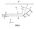
- Fig. 2 is a diagram illustrating a light source apparatus 10 seen in the direction of the arrow A shown in Fig. 1 .
- Fig. 3 is a top view illustrating a part of the light source apparatus 10.
- the light source apparatus 10 includes a plurality of light-emitting elements 2 provided, for example, in one direction (X direction) in a straight manner, and a light guide 3 for guiding in a predetermined direction the light output from the light-emitting elements 2.
- the light-emitting elements 2 are provided on a printed circuit board 8, for example.
- Each of the plurality of light-emitting elements 2 uses an LED having three light-emitting sources of red, green, and blue (RGB).
- RGB red, green, and blue
- one light-emitting element 2 may also be configured to have one single-color light-emitting source or a plurality of single-color light-emitting sources.
- each light-emitting element 2 emits light of each color of R, G, or B, for example, and the light of the respective colors are mixed by the light guide 3.
- the LED may be an inorganic LED or an organic LED.
- the light guide 3 includes an incident surface 7, an emitting surface 6, a reflecting surface (main reflecting surface) 61, and a light guide section 5 including those surfaces 7, 6, and 61.
- Light from the plurality of light-emitting elements 2 enters the incident surface 7.
- the light guide section 5 reflects the light having entered from the incident surface 7 and causes the light to be reflected by the reflecting surface 61 opposed to the incident surface 7 to thereby guide the light to the emitting surface 6. Then, the light exits from the emitting surface 6.
- the light guide 3 (the light guide section 5) is provided to be bent at the middle from the incident surface 7 to the emitting surface 6.
- the wording "to be bent" means to include a shape as shown in Fig. 2 that has a clear folding line or a curved shape that has an unclear folding line.
- the light guide 3 is formed by an integral molding.
- the light guide 3 may be typically made of an acrylic resin, but may also be made of glass, polycarbonate, or other transparent resins.
- the incident surface 7 is formed as a flat surface, for example.
- the incident surface 7 has a width w1 in the Z direction (a width in the height direction) that is designed to be substantially the same width as that of a surface through which light is emitted from the light-emitting element 2 or a width slightly smaller than the width of the surface through which light is emitted from the light-emitting element 2.
- the emitting surface 6 is also formed as a flat surface.
- Fig. 4 is a perspective view illustrating the light guide 3 seen from the reflecting surface 61 side.
- Fig. 5 is a diagram illustrating a part of the reflecting surface 61 seen from the front side of the reflecting surface 61.
- the reflecting surface 61 includes a plurality of microlenses 62 as a plurality of lenses that have optical power at least in the arrangement direction of the light-emitting elements 2 and a direction different from the arrangement direction.
- each of the microlenses 62 is formed to have a convex spherical or aspherical shape toward the outer side of the light guide 3 and the microlenses 62 are arranged in a two-dimensional manner.
- the respective microlenses 62 have optical power in a direction around optical axes of the respective microlenses 62.
- the respective microlenses 62 have a function to cause the light having entered through the incident surface 7 to be uniformly diffused and reflected in the light guide 3.
- the microlenses 62 arranged in the two-dimensional manner typically form a honeycomb configuration. This configuration allows the microlenses 62 to be arranged on the reflecting surface 61 without gaps thereamong, thus reducing nonuniform illuminance.
- Fig. 6 is an expanded view of a bottom surface 63 (which is a surface that is provided between the incident surface 7 and the reflecting surface 61 and that is provided so as to be opposed to the emitting surface 6) and the reflecting surface 61 in Fig. 2 .
- an angle obtained by adding an angle ⁇ 1(°) of the two-dimensional arrangement surface of the respective microlenses 62 to the bottom surface 63 and a maximum inclination angle ⁇ 2(°) of the surfaces of the respective microlenses 62 to the two-dimensional arrangement surface is 120 or more.
- ⁇ 1+ ⁇ 2 ⁇ 120 is established.
- the relation of ⁇ 1+ ⁇ 2 ⁇ 132 is more preferred. The reason will be described below.
- Fig. 7 is a diagram for explaining the reason.
- Fig. 7 shows that light B passing from the left to the right in a medium of the light guide 3 is reflected by the reflecting surface 61.
- the angle of the reflecting surface 61 is drawn as an angle including the maximum inclination angle ⁇ 2 of the microlenses 62 and is assumed as ⁇ 1+ ⁇ 2.
- Most of the light B having entered through the incident surface of the light guide 3 proceeds to be substantially parallel to the bottom surface 63 until reaching the reflecting surface 61.
- This light enters the reflecting surface 61 at an incidence angle ⁇ 4.
- the incidence angle ⁇ 4 to the reflecting surface 61 becomes closer to an angle causing total reflection (critical angle)
- the light use efficiency in the light guide 3 becomes higher.
- the incidence angle ⁇ 4 is equal to or higher than 42° that is the critical angle of the light guide 3, light has total reflection at the reflecting surface 61.
- This is a critical angle of a transparent resin such as acrylic or glass.
- the upper limit value of ⁇ 1+ ⁇ 2 may be 180°. Although a typical example of ⁇ 1+ ⁇ 2 may be 120° or more as described above, ⁇ 1+ ⁇ 2 may also be 130° or more, or 135° or more.
- the incident light from the incident surface 7 can be uniformly diffused in the light guide 3 by the plurality of microlenses 62.
- the illuminance distribution of the light from the emitting surface 6 can be uniformized.
- the left side shows the illuminance distribution when a light guide in the past is used in which a reflecting surface has a flat surface or a cylindrical surface.
- an optical path length h (see Fig. 2 ) can be made shorter than that of a known product disclosed in Patent Document 1.
- a pitch p see Fig. 3
- the optical path length h is tenuously associated with the arrangement pitch p of the respective light-emitting elements 2, thus providing an improved freedom degree to the design of the light guide 3.
- an approach may be considered not to form the microlens 62 on the reflecting surface 61 but to form a mirror layer of silver for example on the reflecting surface.
- this approach needs a step of forming the mirror layer by vapor deposition, thus causing an additional cost.
- this embodiment can provide the light guide 3 having the microlens 62 formed by a mold.
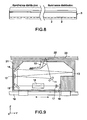
- Fig. 9 is a cross-sectional view illustrating a carriage including the light source apparatus 10.
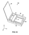
- Fig. 10 is a perspective view illustrating a scanner apparatus as a reading apparatus including this carriage 21.
- the scanner apparatus 100 includes a body 24 having a placing surface 23 on which an irradiation object 22 (see Fig. 2 , Fig. 9 ) such as a document or a photograph is placed, and a cover 25 attached to the body 24 so that the cover 25 can be opened and closed.
- the placing surface 23 is made of, for example, glass or resin having a high light transmittance.
- the body 24 includes therein a motor (not shown), for example, for moving the carriage 21 in a straight direction (Y direction) in order to read the entire surface of the irradiation object 22 placed on the placing surface 23. Furthermore, the body 24 also includes therein guide rails 19 for guiding the move of the carriage 21. The guide rails 19 are connected to the lower part of the carriage 21 as shown in Fig. 10 , for example.
- the configuration of the scanner apparatus 100 is not limited to the shown configuration and may also be subjected to an appropriate design change.
- this carriage 21 includes therein the light source apparatus 10, a plurality of mirrors 11, 12, 13, 14, and 15, a lens system 16 for image formation, an optical path length adjustment element 17, and an image sensor 18 as a photoelectric conversion element.
- the plurality of mirrors 11 to 15 are provided in the manner as described above in order to maximize the optical path length from the light source apparatus 10 to the image sensor 18. These mirrors 11 to 15 have a long shape extending in the X direction.
- the lens system 16 is typically configured by a plurality of lenses.
- the optical path length adjustment element 17 adjusts an optical path difference between infrared light and general light, for example.
- the image sensor 18 may be a CCD, for example.
- the image sensor 18 may also be, in addition to CCD, a complementary metal-oxide semiconductor (CMOS) sensor.
- CMOS complementary metal-oxide semiconductor
- the incident light from the incident surface 7 is uniformly diffused and reflected in the light guide 3 by the plurality of microlenses 62.
- nonuniform illuminance can be reduced even when the glossy irradiation object 22 or the irradiation object 22 having a relatively high reflectivity is read.
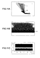
- Figs. 11A and 11B are ray tracing diagrams of the light guide 3 according to this embodiment that are prepared through simulation.
- Fig. 11A is a cross-sectional view.
- Fig. 11B is a top view.
- Fig. 11C is a diagram showing the uniformity of the light guide according to this embodiment, prepared through simulation, and corresponds to the top view of Fig. 11B , in which the horizontal axis shows an X axis direction (see Fig. 1 , for example) and the vertical axis shows a Y axis direction.
- Figs. 12A to 12C correspond to Figs. 11A to 11C , respectively, and illustrate a light guide not having a microlens (a reflecting surface is a flat surface).
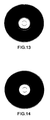
- Fig. 13 is an image of a disk recording medium actually read by the scanner apparatus 100 using the light guide 3 according to this embodiment.
- Fig. 14 is an image of a disk recording medium actually read by a scanner apparatus using a light guide not having a microlens (a reflecting surface is a flat surface).
- Fig. 15 is an image of a disk recording medium read by an apparatus using a light guide optical system according to Patent Document 2 described above. An identical disk recording medium is used in Fig. 13 to Fig. 15 .
- the embodiment according to the present invention is not limited to the above-described embodiment. Various other embodiments may be used.
- the light-emitting element 2 may also be a laser diode instead of the LED.
- any shape of microlenses seen from the front side of the main reflecting surface of the light guide may be used as long as the microlenses have optical power at least in two directions of the arrangement direction thereof and a direction different from the arrangement direction.
- the shape is a circle, an ellipse, a polygon of three or more sides, or for example a combination of at least two of these shapes.
- the microlens may also be formed to have such a shape by which the optical power thereof is different at least in the above two directions, for example.
- a shape of the microlens 62 typically includes an ellipse.
- the ellipse may have a long axis (or a short axis) that corresponds to the arrangement direction of the light-emitting elements 2.
- the illuminance distribution thereof can be changed appropriately.
- the arrangement of the microlenses is not limited to the honeycomb-like regular hexagon one.
- the microlenses may also be arranged in a matrix in the longitudinal and lateral directions or may be arranged randomly.
- the respective microlenses may also have gaps thereamong. Even in such a case, any shape of each microlens seen from the front side of the main reflecting surface may be used as long as the microlens provides an optical power at least in the above two directions.
- the microlens 62 is a convex lens
- the microlens 62 may also be a concave lens.
- the main reflecting surface may have a plurality of concavities to the interior of the light guide.
- the light-emitting elements 2 are arranged in a row.
- the light-emitting elements 2 may also be arranged in a plurality of rows in the Z axis direction.
- the respective light-emitting elements may be arranged to be dislocated from one another (in a honeycomb-like arrangement, for example). If the size of the light-emitting element itself is reduced, the incident surface 7 can have the same area as that of Fig. 1 to thereby increase the number of light-emitting elements.
- the emitting surface of the light guide may be a spherical or an aspherical convex shape.
- the emitting surface may be a flat surface formed by blast processing.
Landscapes
- Physics & Mathematics (AREA)
- General Physics & Mathematics (AREA)
- Optics & Photonics (AREA)
- Engineering & Computer Science (AREA)
- Multimedia (AREA)
- Signal Processing (AREA)
- Microelectronics & Electronic Packaging (AREA)
- Facsimile Scanning Arrangements (AREA)
- Light Sources And Details Of Projection-Printing Devices (AREA)
- Facsimile Heads (AREA)
- Image Input (AREA)
- Planar Illumination Modules (AREA)
Applications Claiming Priority (1)
| Application Number | Priority Date | Filing Date | Title |
|---|---|---|---|
| JP2009215547A JP5499592B2 (ja) | 2009-09-17 | 2009-09-17 | ライトガイド、光源装置及び読取装置 |
Publications (3)
| Publication Number | Publication Date |
|---|---|
| EP2299300A2 EP2299300A2 (en) | 2011-03-23 |
| EP2299300A3 EP2299300A3 (en) | 2012-07-04 |
| EP2299300B1 true EP2299300B1 (en) | 2014-06-18 |
Family
ID=43086522
Family Applications (1)
| Application Number | Title | Priority Date | Filing Date |
|---|---|---|---|
| EP10008195.9A Not-in-force EP2299300B1 (en) | 2009-09-17 | 2010-08-05 | Light guide, light source apparatus, and reading apparatus |
Country Status (5)
| Country | Link |
|---|---|
| US (1) | US8876355B2 (ja) |
| EP (1) | EP2299300B1 (ja) |
| JP (1) | JP5499592B2 (ja) |
| KR (1) | KR20110030318A (ja) |
| CN (1) | CN102022696B (ja) |
Families Citing this family (25)
| Publication number | Priority date | Publication date | Assignee | Title |
|---|---|---|---|---|
| KR20120105810A (ko) * | 2011-03-16 | 2012-09-26 | 삼성디스플레이 주식회사 | 백라이트 어셈블리 및 이를 갖는 표시 장치 |
| EP2742540B1 (en) * | 2011-08-08 | 2016-04-20 | Quarkstar, LLC | Illumination devices including multiple light emitting elements |
| US9081125B2 (en) | 2011-08-08 | 2015-07-14 | Quarkstar Llc | Illumination devices including multiple light emitting elements |
| JP5836723B2 (ja) * | 2011-09-16 | 2015-12-24 | キヤノン株式会社 | 導光体および照明装置並びに画像読取装置 |
| JP5836740B2 (ja) | 2011-09-29 | 2015-12-24 | キヤノン株式会社 | 導光体および照明装置並びに画像読取装置 |
| JP5565775B2 (ja) * | 2011-10-25 | 2014-08-06 | 株式会社栗原工業 | Led照明装置 |
| JP5995459B2 (ja) * | 2012-02-24 | 2016-09-21 | キヤノン株式会社 | 導光体、照明装置、および画像読取装置 |
| JP6016524B2 (ja) * | 2012-08-23 | 2016-10-26 | キヤノン株式会社 | 照明装置および画像読取装置 |
| JP6030388B2 (ja) * | 2012-09-12 | 2016-11-24 | シャープ株式会社 | 冷蔵庫 |
| WO2014043321A1 (en) | 2012-09-13 | 2014-03-20 | Quarkstar Llc | Illumination systems providing direct and indirect illumination |
| WO2014043369A2 (en) | 2012-09-13 | 2014-03-20 | Quarkstar Llc | Devices for workspace illumination |
| US9206956B2 (en) | 2013-02-08 | 2015-12-08 | Quarkstar Llc | Illumination device providing direct and indirect illumination |
| EP2986892B1 (en) | 2013-04-19 | 2017-06-28 | Quarkstar LLC | Illumination devices with adjustable optical elements |
| US9335462B2 (en) | 2013-07-18 | 2016-05-10 | Quarkstar Llc | Luminaire module with multiple light guide elements |
| EP3063471B1 (en) | 2013-09-17 | 2017-07-05 | Quarkstar LLC | Light guide illumination device for direct-indirect illumination |
| KR102163600B1 (ko) * | 2014-06-17 | 2020-10-12 | 엘지디스플레이 주식회사 | 백라이트 유닛 및 이를 구비하는 표시장치 |
| JP6085276B2 (ja) * | 2014-09-29 | 2017-02-22 | 本田技研工業株式会社 | 灯具 |
| US9348080B1 (en) | 2014-11-18 | 2016-05-24 | Quarkstar Llc | Wall wash luminaire with light guide and optical element therefore |
| DE102015001695A1 (de) * | 2015-02-10 | 2016-08-11 | Audi Ag | Beleuchtungsvorrichtung für einen Scheinwerfer eines Kraftfahrzeugs sowie Verfahren zum Betreiben einer Beleuchtungsvorrichtung |
| JP2016171423A (ja) | 2015-03-12 | 2016-09-23 | キヤノン株式会社 | 画像読取装置 |
| US10136020B2 (en) * | 2016-03-18 | 2018-11-20 | Canon Kabushiki Kaisha | Image reading apparatus and image forming apparatus |
| TR201612442A2 (tr) * | 2016-09-02 | 2018-03-21 | Arcelik As | Aydinlatma vasitasi i̇çeren bi̇r firin |
| JP6779737B2 (ja) * | 2016-10-13 | 2020-11-04 | キヤノン株式会社 | 画像読取装置及び画像形成装置 |
| US10330902B1 (en) | 2017-06-16 | 2019-06-25 | Dbm Reflex Enterprises Inc. | Illumination optics and devices |
| EP3743755B1 (en) * | 2018-01-25 | 2022-11-09 | LMPG Inc. | Light guide |
Family Cites Families (12)
| Publication number | Priority date | Publication date | Assignee | Title |
|---|---|---|---|---|
| JP2000358130A (ja) * | 1999-06-15 | 2000-12-26 | Rohm Co Ltd | 画像読み取り装置およびこれに用いる導光用ユニット |
| US6979428B2 (en) * | 2003-08-01 | 2005-12-27 | Steris Inc. | Fluid over-flow/make-up air assembly for reprocessor |
| JP4093990B2 (ja) * | 2004-05-26 | 2008-06-04 | 日本板硝子株式会社 | 導光体、ライン照明装置および画像読取装置 |
| JP2006156368A (ja) * | 2004-11-02 | 2006-06-15 | Hisashi Kojima | 導光板及びバックライト装置 |
| WO2006120932A1 (ja) * | 2005-05-12 | 2006-11-16 | Nippon Sheet Glass Company, Limited | 導光体及び画像読取装置 |
| JP4788577B2 (ja) * | 2006-11-10 | 2011-10-05 | ソニー株式会社 | ライトガイド、光源装置及び電子機器 |
| CN101196576A (zh) * | 2006-12-08 | 2008-06-11 | 鸿富锦精密工业(深圳)有限公司 | 光学板 |
| CN101359065B (zh) * | 2007-07-30 | 2012-03-21 | 亚洲光学股份有限公司 | 导光组件及光源模块 |
| CN101377280A (zh) * | 2007-08-30 | 2009-03-04 | 精碟科技股份有限公司 | 扫描装置的光源模组 |
| JP2009065621A (ja) * | 2007-09-10 | 2009-03-26 | Rohm Co Ltd | 導光体、線状光源、およびイメージセンサモジュール |
| JP5100278B2 (ja) * | 2007-09-25 | 2012-12-19 | キヤノン株式会社 | 導光光学系及びそれを用いた原稿照明装置及びそれを用いた画像読取装置 |
| JP2009093808A (ja) * | 2007-10-03 | 2009-04-30 | Sharp Corp | 照明装置および液晶表示装置 |
-
2009
- 2009-09-17 JP JP2009215547A patent/JP5499592B2/ja not_active Expired - Fee Related
-
2010
- 2010-08-05 EP EP10008195.9A patent/EP2299300B1/en not_active Not-in-force
- 2010-09-03 KR KR1020100086317A patent/KR20110030318A/ko not_active Application Discontinuation
- 2010-09-08 CN CN2010102755883A patent/CN102022696B/zh not_active Expired - Fee Related
- 2010-09-10 US US12/879,533 patent/US8876355B2/en not_active Expired - Fee Related
Also Published As
| Publication number | Publication date |
|---|---|
| EP2299300A3 (en) | 2012-07-04 |
| JP2011065864A (ja) | 2011-03-31 |
| KR20110030318A (ko) | 2011-03-23 |
| US20110063870A1 (en) | 2011-03-17 |
| EP2299300A2 (en) | 2011-03-23 |
| CN102022696A (zh) | 2011-04-20 |
| JP5499592B2 (ja) | 2014-05-21 |
| US8876355B2 (en) | 2014-11-04 |
| CN102022696B (zh) | 2013-04-03 |
Similar Documents
| Publication | Publication Date | Title |
|---|---|---|
| EP2299300B1 (en) | Light guide, light source apparatus, and reading apparatus | |
| US8755096B2 (en) | Image sensor unit and image reading apparatus | |
| TWI461636B (zh) | Light source device | |
| US20050265684A1 (en) | Light, guide, line-illuminating device, and image-scanning device | |
| US20120176801A1 (en) | Flash lens and flash module employing the same | |
| US10536603B2 (en) | Light guide and image reading apparatus | |
| KR20120050179A (ko) | 플래시 렌즈 및 이를 채용한 플래시 모듈 | |
| CN103891262A (zh) | 照明单元以及使用该照明单元的图像读取装置 | |
| JP2010003597A (ja) | Led灯具ユニット | |
| JP6129602B2 (ja) | 原稿読取用光源装置 | |
| CN1637571A (zh) | 光偏转器和背面投射屏 | |
| CA3061625C (en) | Total internal reflection lens to lessen glare and maintain color mixing and beam control | |
| JP6261112B2 (ja) | イメージセンサーユニット及び画像読取装置 | |
| KR20120079665A (ko) | 카메라 플래시 발광소자용 렌즈 | |
| JP6150020B2 (ja) | 導光体、光源装置および画像読取装置 | |
| KR100902044B1 (ko) | 전반사를 이용한 카메라 플래시 장치 | |
| JP6087069B2 (ja) | ドキュメントスキャナ | |
| US20090213441A1 (en) | Light source device and original document reading device | |
| CN102540317A (zh) | 导光元件及高均匀度高亮度光源模组 | |
| WO2024013899A1 (ja) | 導光体、照明装置および密着型イメージセンサ | |
| JPWO2019003480A1 (ja) | 導光体及び画像読取装置 | |
| JP7341319B2 (ja) | 照明装置及びイメージスキャナ | |
| JP2008076599A (ja) | 照明装置、読取装置、及び画像処理装置 | |
| JP6720022B2 (ja) | 照明装置及び画像読取装置 | |
| JP7025116B2 (ja) | 照明装置及び画像読取装置 |
Legal Events
| Date | Code | Title | Description |
|---|---|---|---|
| PUAI | Public reference made under article 153(3) epc to a published international application that has entered the european phase |
Free format text: ORIGINAL CODE: 0009012 |
|
| 17P | Request for examination filed |
Effective date: 20100805 |
|
| AK | Designated contracting states |
Kind code of ref document: A2 Designated state(s): AL AT BE BG CH CY CZ DE DK EE ES FI FR GB GR HR HU IE IS IT LI LT LU LV MC MK MT NL NO PL PT RO SE SI SK SM TR |
|
| AX | Request for extension of the european patent |
Extension state: BA ME RS |
|
| PUAL | Search report despatched |
Free format text: ORIGINAL CODE: 0009013 |
|
| AK | Designated contracting states |
Kind code of ref document: A3 Designated state(s): AL AT BE BG CH CY CZ DE DK EE ES FI FR GB GR HR HU IE IS IT LI LT LU LV MC MK MT NL NO PL PT RO SE SI SK SM TR |
|
| AX | Request for extension of the european patent |
Extension state: BA ME RS |
|
| RIC1 | Information provided on ipc code assigned before grant |
Ipc: G02B 6/00 20060101AFI20120529BHEP |
|
| 17Q | First examination report despatched |
Effective date: 20130212 |
|
| REG | Reference to a national code |
Ref country code: DE Ref legal event code: R079 Ref document number: 602010016731 Country of ref document: DE Free format text: PREVIOUS MAIN CLASS: G02B0006000000 Ipc: F21V0008000000 |
|
| RIC1 | Information provided on ipc code assigned before grant |
Ipc: H04N 1/028 20060101ALI20131115BHEP Ipc: F21V 8/00 20060101AFI20131115BHEP |
|
| GRAP | Despatch of communication of intention to grant a patent |
Free format text: ORIGINAL CODE: EPIDOSNIGR1 |
|
| INTG | Intention to grant announced |
Effective date: 20140108 |
|
| GRAS | Grant fee paid |
Free format text: ORIGINAL CODE: EPIDOSNIGR3 |
|
| GRAA | (expected) grant |
Free format text: ORIGINAL CODE: 0009210 |
|
| AK | Designated contracting states |
Kind code of ref document: B1 Designated state(s): AL AT BE BG CH CY CZ DE DK EE ES FI FR GB GR HR HU IE IS IT LI LT LU LV MC MK MT NL NO PL PT RO SE SI SK SM TR |
|
| REG | Reference to a national code |
Ref country code: GB Ref legal event code: FG4D |
|
| REG | Reference to a national code |
Ref country code: CH Ref legal event code: EP |
|
| REG | Reference to a national code |
Ref country code: AT Ref legal event code: REF Ref document number: 673557 Country of ref document: AT Kind code of ref document: T Effective date: 20140715 |
|
| REG | Reference to a national code |
Ref country code: IE Ref legal event code: FG4D |
|
| REG | Reference to a national code |
Ref country code: DE Ref legal event code: R096 Ref document number: 602010016731 Country of ref document: DE Effective date: 20140814 |
|
| PG25 | Lapsed in a contracting state [announced via postgrant information from national office to epo] |
Ref country code: NO Free format text: LAPSE BECAUSE OF FAILURE TO SUBMIT A TRANSLATION OF THE DESCRIPTION OR TO PAY THE FEE WITHIN THE PRESCRIBED TIME-LIMIT Effective date: 20140918 Ref country code: CY Free format text: LAPSE BECAUSE OF FAILURE TO SUBMIT A TRANSLATION OF THE DESCRIPTION OR TO PAY THE FEE WITHIN THE PRESCRIBED TIME-LIMIT Effective date: 20140618 Ref country code: LT Free format text: LAPSE BECAUSE OF FAILURE TO SUBMIT A TRANSLATION OF THE DESCRIPTION OR TO PAY THE FEE WITHIN THE PRESCRIBED TIME-LIMIT Effective date: 20140618 Ref country code: FI Free format text: LAPSE BECAUSE OF FAILURE TO SUBMIT A TRANSLATION OF THE DESCRIPTION OR TO PAY THE FEE WITHIN THE PRESCRIBED TIME-LIMIT Effective date: 20140618 Ref country code: GR Free format text: LAPSE BECAUSE OF FAILURE TO SUBMIT A TRANSLATION OF THE DESCRIPTION OR TO PAY THE FEE WITHIN THE PRESCRIBED TIME-LIMIT Effective date: 20140919 |
|
| PGFP | Annual fee paid to national office [announced via postgrant information from national office to epo] |
Ref country code: DE Payment date: 20140821 Year of fee payment: 5 |
|
| REG | Reference to a national code |
Ref country code: NL Ref legal event code: VDEP Effective date: 20140618 |
|
| REG | Reference to a national code |
Ref country code: AT Ref legal event code: MK05 Ref document number: 673557 Country of ref document: AT Kind code of ref document: T Effective date: 20140618 |
|
| REG | Reference to a national code |
Ref country code: LT Ref legal event code: MG4D |
|
| PG25 | Lapsed in a contracting state [announced via postgrant information from national office to epo] |
Ref country code: LV Free format text: LAPSE BECAUSE OF FAILURE TO SUBMIT A TRANSLATION OF THE DESCRIPTION OR TO PAY THE FEE WITHIN THE PRESCRIBED TIME-LIMIT Effective date: 20140618 Ref country code: SE Free format text: LAPSE BECAUSE OF FAILURE TO SUBMIT A TRANSLATION OF THE DESCRIPTION OR TO PAY THE FEE WITHIN THE PRESCRIBED TIME-LIMIT Effective date: 20140618 Ref country code: HR Free format text: LAPSE BECAUSE OF FAILURE TO SUBMIT A TRANSLATION OF THE DESCRIPTION OR TO PAY THE FEE WITHIN THE PRESCRIBED TIME-LIMIT Effective date: 20140618 |
|
| PGFP | Annual fee paid to national office [announced via postgrant information from national office to epo] |
Ref country code: FR Payment date: 20140821 Year of fee payment: 5 |
|
| PG25 | Lapsed in a contracting state [announced via postgrant information from national office to epo] |
Ref country code: SK Free format text: LAPSE BECAUSE OF FAILURE TO SUBMIT A TRANSLATION OF THE DESCRIPTION OR TO PAY THE FEE WITHIN THE PRESCRIBED TIME-LIMIT Effective date: 20140618 Ref country code: PT Free format text: LAPSE BECAUSE OF FAILURE TO SUBMIT A TRANSLATION OF THE DESCRIPTION OR TO PAY THE FEE WITHIN THE PRESCRIBED TIME-LIMIT Effective date: 20141020 Ref country code: RO Free format text: LAPSE BECAUSE OF FAILURE TO SUBMIT A TRANSLATION OF THE DESCRIPTION OR TO PAY THE FEE WITHIN THE PRESCRIBED TIME-LIMIT Effective date: 20140618 Ref country code: CZ Free format text: LAPSE BECAUSE OF FAILURE TO SUBMIT A TRANSLATION OF THE DESCRIPTION OR TO PAY THE FEE WITHIN THE PRESCRIBED TIME-LIMIT Effective date: 20140618 Ref country code: EE Free format text: LAPSE BECAUSE OF FAILURE TO SUBMIT A TRANSLATION OF THE DESCRIPTION OR TO PAY THE FEE WITHIN THE PRESCRIBED TIME-LIMIT Effective date: 20140618 Ref country code: ES Free format text: LAPSE BECAUSE OF FAILURE TO SUBMIT A TRANSLATION OF THE DESCRIPTION OR TO PAY THE FEE WITHIN THE PRESCRIBED TIME-LIMIT Effective date: 20140618 |
|
| PG25 | Lapsed in a contracting state [announced via postgrant information from national office to epo] |
Ref country code: NL Free format text: LAPSE BECAUSE OF FAILURE TO SUBMIT A TRANSLATION OF THE DESCRIPTION OR TO PAY THE FEE WITHIN THE PRESCRIBED TIME-LIMIT Effective date: 20140618 Ref country code: PL Free format text: LAPSE BECAUSE OF FAILURE TO SUBMIT A TRANSLATION OF THE DESCRIPTION OR TO PAY THE FEE WITHIN THE PRESCRIBED TIME-LIMIT Effective date: 20140618 Ref country code: AT Free format text: LAPSE BECAUSE OF FAILURE TO SUBMIT A TRANSLATION OF THE DESCRIPTION OR TO PAY THE FEE WITHIN THE PRESCRIBED TIME-LIMIT Effective date: 20140618 Ref country code: IS Free format text: LAPSE BECAUSE OF FAILURE TO SUBMIT A TRANSLATION OF THE DESCRIPTION OR TO PAY THE FEE WITHIN THE PRESCRIBED TIME-LIMIT Effective date: 20141018 |
|
| REG | Reference to a national code |
Ref country code: DE Ref legal event code: R097 Ref document number: 602010016731 Country of ref document: DE |
|
| PG25 | Lapsed in a contracting state [announced via postgrant information from national office to epo] |
Ref country code: LU Free format text: LAPSE BECAUSE OF FAILURE TO SUBMIT A TRANSLATION OF THE DESCRIPTION OR TO PAY THE FEE WITHIN THE PRESCRIBED TIME-LIMIT Effective date: 20140805 Ref country code: MC Free format text: LAPSE BECAUSE OF FAILURE TO SUBMIT A TRANSLATION OF THE DESCRIPTION OR TO PAY THE FEE WITHIN THE PRESCRIBED TIME-LIMIT Effective date: 20140618 |
|
| REG | Reference to a national code |
Ref country code: CH Ref legal event code: PL |
|
| PLBE | No opposition filed within time limit |
Free format text: ORIGINAL CODE: 0009261 |
|
| STAA | Information on the status of an ep patent application or granted ep patent |
Free format text: STATUS: NO OPPOSITION FILED WITHIN TIME LIMIT |
|
| PG25 | Lapsed in a contracting state [announced via postgrant information from national office to epo] |
Ref country code: BE Free format text: LAPSE BECAUSE OF NON-PAYMENT OF DUE FEES Effective date: 20140831 Ref country code: LI Free format text: LAPSE BECAUSE OF NON-PAYMENT OF DUE FEES Effective date: 20140831 Ref country code: CH Free format text: LAPSE BECAUSE OF NON-PAYMENT OF DUE FEES Effective date: 20140831 Ref country code: IT Free format text: LAPSE BECAUSE OF FAILURE TO SUBMIT A TRANSLATION OF THE DESCRIPTION OR TO PAY THE FEE WITHIN THE PRESCRIBED TIME-LIMIT Effective date: 20140618 Ref country code: DK Free format text: LAPSE BECAUSE OF FAILURE TO SUBMIT A TRANSLATION OF THE DESCRIPTION OR TO PAY THE FEE WITHIN THE PRESCRIBED TIME-LIMIT Effective date: 20140618 |
|
| REG | Reference to a national code |
Ref country code: IE Ref legal event code: MM4A |
|
| 26N | No opposition filed |
Effective date: 20150319 |
|
| GBPC | Gb: european patent ceased through non-payment of renewal fee |
Effective date: 20140918 |
|
| PG25 | Lapsed in a contracting state [announced via postgrant information from national office to epo] |
Ref country code: BE Free format text: LAPSE BECAUSE OF FAILURE TO SUBMIT A TRANSLATION OF THE DESCRIPTION OR TO PAY THE FEE WITHIN THE PRESCRIBED TIME-LIMIT Effective date: 20140618 |
|
| PG25 | Lapsed in a contracting state [announced via postgrant information from national office to epo] |
Ref country code: GB Free format text: LAPSE BECAUSE OF NON-PAYMENT OF DUE FEES Effective date: 20140918 Ref country code: SI Free format text: LAPSE BECAUSE OF FAILURE TO SUBMIT A TRANSLATION OF THE DESCRIPTION OR TO PAY THE FEE WITHIN THE PRESCRIBED TIME-LIMIT Effective date: 20140618 |
|
| PG25 | Lapsed in a contracting state [announced via postgrant information from national office to epo] |
Ref country code: IE Free format text: LAPSE BECAUSE OF NON-PAYMENT OF DUE FEES Effective date: 20140805 |
|
| REG | Reference to a national code |
Ref country code: DE Ref legal event code: R119 Ref document number: 602010016731 Country of ref document: DE |
|
| PG25 | Lapsed in a contracting state [announced via postgrant information from national office to epo] |
Ref country code: SM Free format text: LAPSE BECAUSE OF FAILURE TO SUBMIT A TRANSLATION OF THE DESCRIPTION OR TO PAY THE FEE WITHIN THE PRESCRIBED TIME-LIMIT Effective date: 20140618 |
|
| REG | Reference to a national code |
Ref country code: FR Ref legal event code: ST Effective date: 20160429 |
|
| PG25 | Lapsed in a contracting state [announced via postgrant information from national office to epo] |
Ref country code: MT Free format text: LAPSE BECAUSE OF FAILURE TO SUBMIT A TRANSLATION OF THE DESCRIPTION OR TO PAY THE FEE WITHIN THE PRESCRIBED TIME-LIMIT Effective date: 20140618 Ref country code: BG Free format text: LAPSE BECAUSE OF FAILURE TO SUBMIT A TRANSLATION OF THE DESCRIPTION OR TO PAY THE FEE WITHIN THE PRESCRIBED TIME-LIMIT Effective date: 20140618 |
|
| PG25 | Lapsed in a contracting state [announced via postgrant information from national office to epo] |
Ref country code: TR Free format text: LAPSE BECAUSE OF FAILURE TO SUBMIT A TRANSLATION OF THE DESCRIPTION OR TO PAY THE FEE WITHIN THE PRESCRIBED TIME-LIMIT Effective date: 20140618 Ref country code: DE Free format text: LAPSE BECAUSE OF NON-PAYMENT OF DUE FEES Effective date: 20160301 Ref country code: HU Free format text: LAPSE BECAUSE OF FAILURE TO SUBMIT A TRANSLATION OF THE DESCRIPTION OR TO PAY THE FEE WITHIN THE PRESCRIBED TIME-LIMIT; INVALID AB INITIO Effective date: 20100805 |
|
| PG25 | Lapsed in a contracting state [announced via postgrant information from national office to epo] |
Ref country code: FR Free format text: LAPSE BECAUSE OF NON-PAYMENT OF DUE FEES Effective date: 20150831 |
|
| PG25 | Lapsed in a contracting state [announced via postgrant information from national office to epo] |
Ref country code: MK Free format text: LAPSE BECAUSE OF FAILURE TO SUBMIT A TRANSLATION OF THE DESCRIPTION OR TO PAY THE FEE WITHIN THE PRESCRIBED TIME-LIMIT Effective date: 20140618 |
|
| PG25 | Lapsed in a contracting state [announced via postgrant information from national office to epo] |
Ref country code: AL Free format text: LAPSE BECAUSE OF FAILURE TO SUBMIT A TRANSLATION OF THE DESCRIPTION OR TO PAY THE FEE WITHIN THE PRESCRIBED TIME-LIMIT Effective date: 20140618 |