EP2290716B1 - LED-Modul - Google Patents
LED-Modul Download PDFInfo
- Publication number
- EP2290716B1 EP2290716B1 EP10184330.8A EP10184330A EP2290716B1 EP 2290716 B1 EP2290716 B1 EP 2290716B1 EP 10184330 A EP10184330 A EP 10184330A EP 2290716 B1 EP2290716 B1 EP 2290716B1
- Authority
- EP
- European Patent Office
- Prior art keywords
- outer dam
- led module
- dam
- module according
- led
- Prior art date
- Legal status (The legal status is an assumption and is not a legal conclusion. Google has not performed a legal analysis and makes no representation as to the accuracy of the status listed.)
- Active
Links
Images

Classifications
-
- H—ELECTRICITY
- H10—SEMICONDUCTOR DEVICES; ELECTRIC SOLID-STATE DEVICES NOT OTHERWISE PROVIDED FOR
- H10H—INORGANIC LIGHT-EMITTING SEMICONDUCTOR DEVICES HAVING POTENTIAL BARRIERS
- H10H20/00—Individual inorganic light-emitting semiconductor devices having potential barriers, e.g. light-emitting diodes [LED]
- H10H20/80—Constructional details
- H10H20/85—Packages
- H10H20/852—Encapsulations
-
- H—ELECTRICITY
- H10—SEMICONDUCTOR DEVICES; ELECTRIC SOLID-STATE DEVICES NOT OTHERWISE PROVIDED FOR
- H10F—INORGANIC SEMICONDUCTOR DEVICES SENSITIVE TO INFRARED RADIATION, LIGHT, ELECTROMAGNETIC RADIATION OF SHORTER WAVELENGTH OR CORPUSCULAR RADIATION
- H10F77/00—Constructional details of devices covered by this subclass
- H10F77/30—Coatings
- H10F77/306—Coatings for devices having potential barriers
-
- H—ELECTRICITY
- H10—SEMICONDUCTOR DEVICES; ELECTRIC SOLID-STATE DEVICES NOT OTHERWISE PROVIDED FOR
- H10F—INORGANIC SEMICONDUCTOR DEVICES SENSITIVE TO INFRARED RADIATION, LIGHT, ELECTROMAGNETIC RADIATION OF SHORTER WAVELENGTH OR CORPUSCULAR RADIATION
- H10F77/00—Constructional details of devices covered by this subclass
- H10F77/50—Encapsulations or containers
-
- H—ELECTRICITY
- H10—SEMICONDUCTOR DEVICES; ELECTRIC SOLID-STATE DEVICES NOT OTHERWISE PROVIDED FOR
- H10H—INORGANIC LIGHT-EMITTING SEMICONDUCTOR DEVICES HAVING POTENTIAL BARRIERS
- H10H20/00—Individual inorganic light-emitting semiconductor devices having potential barriers, e.g. light-emitting diodes [LED]
- H10H20/80—Constructional details
- H10H20/85—Packages
- H10H20/855—Optical field-shaping means, e.g. lenses
- H10H20/856—Reflecting means
-
- H—ELECTRICITY
- H10—SEMICONDUCTOR DEVICES; ELECTRIC SOLID-STATE DEVICES NOT OTHERWISE PROVIDED FOR
- H10H—INORGANIC LIGHT-EMITTING SEMICONDUCTOR DEVICES HAVING POTENTIAL BARRIERS
- H10H20/00—Individual inorganic light-emitting semiconductor devices having potential barriers, e.g. light-emitting diodes [LED]
- H10H20/80—Constructional details
- H10H20/85—Packages
- H10H20/852—Encapsulations
- H10H20/854—Encapsulations characterised by their material, e.g. epoxy or silicone resins
-
- H—ELECTRICITY
- H10—SEMICONDUCTOR DEVICES; ELECTRIC SOLID-STATE DEVICES NOT OTHERWISE PROVIDED FOR
- H10W—GENERIC PACKAGES, INTERCONNECTIONS, CONNECTORS OR OTHER CONSTRUCTIONAL DETAILS OF DEVICES COVERED BY CLASS H10
- H10W74/00—Encapsulations, e.g. protective coatings
-
- H—ELECTRICITY
- H10—SEMICONDUCTOR DEVICES; ELECTRIC SOLID-STATE DEVICES NOT OTHERWISE PROVIDED FOR
- H10W—GENERIC PACKAGES, INTERCONNECTIONS, CONNECTORS OR OTHER CONSTRUCTIONAL DETAILS OF DEVICES COVERED BY CLASS H10
- H10W90/00—Package configurations
- H10W90/701—Package configurations characterised by the relative positions of pads or connectors relative to package parts
- H10W90/751—Package configurations characterised by the relative positions of pads or connectors relative to package parts of bond wires
- H10W90/756—Package configurations characterised by the relative positions of pads or connectors relative to package parts of bond wires between a chip and a stacked lead frame, conducting package substrate or heat sink
Definitions
- the present invention relates to the field of light emitting diode (LED) modules comprising a LED chip mounted on a board, and a cover.
- the cover is designed to allow the directed passage of light from the LED chip.
- COB chip-on-board
- LED modules with a so called globe-top which is based on a heat-curable resin.
- a globe-top is usually applied with standard dispensing equipment.
- the performance of LED modules having such a globe-top is not satisfying all requirements of different application fields.
- One of the main disadvantages actually is the directive characteristics, i.e. the wide emission angle, which is not well suited for using such a LED module with secondary optics, such as for example lenses or light guides.
- the LED chip In order to have a smaller emission angle of the light emitted by COB LED modules the LED chip is sometimes placed in a cavity with a reflecting wall. However, due to the spherical shape of the top surface of the globe-top, the contribution of the reflecting wall on the emission angle is not satisfying.
- the second disadvantage of the globe-top cover is the low mechanical stability of the LED modules which is a disadvantage for the handling and mounting of the LED modules.
- silicones are used as resins for the globe-top.
- these rubber-like materials apply a high mechanical stress to bond wires if the spherical shape of the globe-top is warped.
- WO 2006/017484A1 proposes a dam-and-fill technology in order to protect parts of a printed circuit board against electric short circuits.
- DE 10245946 C1 discloses a LED module comprising a LED chip mounted on a board, a cured silicone resin dam comprising reflecting TiO 2 particles dispensed on the board, and a transparent cured resin filled into the dam.
- US 5,851,847 discloses a LED module comprising a LED chip mounted on a board, a cured silicone resin dam dispensed on the board, and a transparent cured silicone resin filled into the dam, wherein the silicone filling is chemically linked to the dam across the interface between the two materials.
- JP 2006-066786 discloses a LED module comprising a LED chip mounted on a board, a transparent cured silicone resin dam dispensed on the board, and a transparent cured silicone resin comprising colour conversion particles filled into the dam.
- the over comprises an outer non-transparent and reflective dam and a central filling, which central filling has been filled into the outer dam preferably after the manufacturing of the outer dam.
- the outer dam and the central filling are respectively made from a cured silicone based resin and a cured transparent resin.
- the central filling is chemically linked to the outer dam across the interface between the two materials.
- outer dam does not represent any limitation as to the shape, as long as the dam can act as a dam surrounding the central filling and being stable in shape even in the uncured state.
- the resin of the central filling can be e.g. silicone.
- the resin of the outer dam comprises reflecting particles which are white pigments.
- the reflecting particles are preferably present throughout the bulk of the outer dam material.
- the dam thus has the role of a reflector applied in the liquid state on a board.
- the outer dam can comprise 10 to 60 weight % of the reflecting particles.
- the resin of the outer dam and the central filling can have the same chemical structure, e.g. they can be chemically identical.
- the resin of the outer dam can be selected to have a storage modulus of more than 1000 Pa before being cured.
- the resin of the outer dam can be selected such that it has for example a viscosity of more than 100 Pa*s when measured at a shear rate of 1 1/s, again before being cured.
- the material of the outer dam can comprise particulate material such as e.g. silica, which particular material or fine grained material can be used in order to set the desired rheological properties of the uncured dam resin.
- particulate material such as e.g. silica, which particular material or fine grained material can be used in order to set the desired rheological properties of the uncured dam resin.
- the height of the outer dam can be equal to or more than 1mm.
- the mean thickness of the outer dam can be selected according to the requirements of the final element. For a diameter of approx. 5 mm the thickness can be equal to or less than 0.5mm. For larger diameters the thickness is adjusted to more than 0.5 mm, for smaller diameters the thickness might be less than 0.5 mm.
- the inner diameter of the dam can be as small as e.g. 0.1 to 1mm.
- the cover comprises an outer dam and a central filling, which has been filled into the outer dam and at least partially on top of the LED chip after the outer dam has been made on the board surrounding the LED chip.
- the central filling is made from a cured transparent resin, such as e.g. silicone.
- the central filling comprises color conversion particles which convert light emitted from the LED chip into light of a second, lower frequency spectrum.
- the inner wall of the outer dam can be distanced from the LED chip, such that the distance between the outer dam and the LED chip is filled with the central filling which thus is also in contact with the board on which the LED chip is mounted e.g. in a chip-on-board technology.
- the central filling can fill the entire volume defined by the outer dam such that the top surface of the filling is on the same level as the maximum height of the outer dam.
- the outer dam is raised higher from the board than the LED-chip.
- an outer dam made from a liquid resin is first dispensed. This outer dam is then filled with a liquid resin. Finally, in one single step, the resin of the outer dam and the resin of the central filling are cured and a chemically linked interface between the outer dam and the central filling is provided which guarantees a stronger adhesion between the central filling and the outer dam.
- a ring-shaped dam (torus) of a liquid resin is dispensed around the LED chip 1, which is mounted on a board 4.
- a plane board without recessions is used, as the reflective effect of walls of a recession can be achieved by the dam walls.
- Dispensing techniques for resins and silicones are known as such from the prior art. Due to the dispensing technique the cross-sectional view of the dam tapers to the peak 10 of the dam 2. Thus the inner face 11 of dam 2 is inclined and preferably is steeper at its upper part which can be of advantage for reflection purposes.
- the cross-sectional shape of the dam 2 can be controlled by the diameter of the dispensing needle used, the flow characteristics of the liquid dam material and the flow (dispensing) speed.
- the LED chip 1 is mounted according to the chip-on-board (COB) technology.
- the bond wires are designated with the reference numeral 5.
- the wall of liquid resin is dispensed on the board 4 around the LED die 1 thus forming a dam.
- the dam material is non-transparent for the wavelength of the light passing through the central filling inside the dam.
- outer dam in the context of the present description and claims does not constitute any limitation as to the contour of the walls, i.e. the dam does not necessarily have a spherical shape, but can e.g. have the shape of a square, an oval, a rectangular shape etc..
- the circular shape is preferred if only a single LED chip is placed inside the dam (see later on), while a rectangular or oval shape is preferred in case a plurality of LED chips are placed inside the dam in a row configuration.
- Silicone materials are known for their high UV stability.
- the rheological characteristics of the liquid resin material for building the wall of the dam 2 have to be well selected such that after the dispensing the uncured resin is stable in shape until it is cured.
- the storage modulus should be rather high and e.g. be at least 1000 Pa.
- the loss factor should be approximately 0.5.
- the viscosity of the liquid resin should preferably be higher than 200 Pa*s (when measured at a shear rate of 1 1/s).
- a liquid resin material of such characteristics is suited for achieving a wall e.g. with a height of more than 1mm and a mean thickness of less than 0.5mm.
- silica or other particulate material can be added to the liquid resin.
- the wall 2 is distanced from the LED die 1.
- the height of the dam 2 is set to be higher than the height of the LED die 1.
- the height of the dam 2 can be twice or three times the height of the LED die 1.
- reflecting white pigments made from TiO 2 , BaTiO 3 , BaSO 4 and/or ZrO 2 are added into the liquid resin.
- these pigments are added to the liquid resin in an amount of 10% to 60% per weight.
- the entire material of the dam will have a non-transparent and white reflecting appearance.
- the reflection from light from the LED die 1 occurs at the inner face 11 of the dam 2 reflecting light back to the interior of the dam 2 and away from the LED die 1.
- the volume confined by the inner walls of the self-stable dam 2 is filled with a liquid filling material.
- this filling is preferably made such that the top level of the filling flushes with the top level of the walls of the dam 2. Due to the filling with the liquid resin the top surface 12 of the central filling 3 will be preferably flat.
- liquid uncured resin is filled in a cavity defined by a self-stable dam of uncured resin, which preferably chemically identical, but can be different regarding optical and mechanical characteristics (as the material of the outer dam 2 and is provided with different "additives" as the material of the central filling 3).
- the chemical identity has to be such that the material used for the dam and the filling, respectively, can be cured using the same curing mechanism in order to produce a chemical linking across the interface between the two materials.
- the filling material entirely covers the top surface of the LED die 1. It also covers the space between the LED die 1 and the walls of the dam 2 (if any) and contacts the board 4 in this gap between the LED die 1 and the dam 2.
- the transparent material for the central filling 3 is also a resin and can be e.g. be made from a silicone material.
- the resin for the central filling 3 is made from the same material as the resin for the dam 2 such that these resins are chemically identical.
- white color-conversion LED modules are provided, in which colour conversion particles are added to the fill material of the central filling 3.
- the type and the amount of the colour conversion particles depends on the desired colour temperature of the LED module, which is known as such from the prior art.
- liquid resins i.e. the resins of the central filling 3 and the dam 2 are cured.
- both of the materials can be cured and chemically linked together at their interface.
- the above-outlined manufacturing process relies on a relatively high mechanical stability of the material of the wall in the uncured "liquid” state. Again, in order to achieve this mechanical stability in the liquid state, additional filling materials such as for example silica can be added to the resin for the dam 2.
- Figures 2 and 3 show a top view ( Fig. 2 ) and a perspective view ( Fig. 3 ) of a LED module according to the present invention comprising a LED chip mounted in chip-on-board technology.
- the material of the dam 2 is highly reflective as white pigments have been added throughout the base resin for the dam 2.
- the resin for the filling 3 is transparent and the bond wires 5 can be seen which are surrounded and stabilized by the material of the central filling 3.
- a light-erasable memory device such as for example an EEPROM 7, not forming part of the present invention, is shown.
- the cover can protect the opening 6 of the casing of the light erasable memory device 7, which opening is designed for the light erasing process.
- the "dam-and-fill" cover which can be made of highly transparent materials depending on the requirements of the erasing/programming light beam, a protection against environmental influences as well as perfect fit to the erasing/programming light source can be achieved. Especially, the protection against scattered light and stray light is a big advantage of the dam and fill cover.
- the outer dam thus can not only serve as a reflective element, but additionally or alternatively as an opaque shielding.
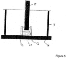
- Fig. 5 shows the use of a LED module according to the present invention in connection with light guides and optical fibers.
- the dam material 2 provides a mechanical stability, such that it is possible to provide the filling 3 on top of the light source as a very fluid and highly transparent synthetic resin.
- the filling 3 is not completely flush with the top of the wall of the dam 2.
- the reference sign 8 designates an optical fiber to which light from the LED chip 1 is to be transmitted (transversing the fill material 3).
- the reference sign 9 designates mechanical fixture for optical fibers.
- the arrangement as shown in Fig. 5 provides for an improved light feeding from the LED chip to the optical fibre.
Landscapes
- Led Device Packages (AREA)
- Structures Or Materials For Encapsulating Or Coating Semiconductor Devices Or Solid State Devices (AREA)
- Encapsulation Of And Coatings For Semiconductor Or Solid State Devices (AREA)
Claims (17)
- LED-Modul, umfassend einen LED-Chip (1), der auf einer Platine (4) montiert ist, und eine Abdeckung,- die Abdeckung umfassend einen äußeren Damm (2), der auf der
Platine verteilt ist, und- eine mittige Füllung (3), die in den äußeren Damm (2) gefüllt ist,wobei der äußere Damm (2) aus einem gehärteten Harz auf Silikonbasis besteht,
wobei die mittige Füllung (3) aus einem gehärteten transparenten Harz besteht, und
wobei die mittige Füllung (3) Partikel zur Farbkonvertierung umfasst, dadurch gekennzeichnet, dass der äußere Damm (2) nicht transparent ist und reflektierende Partikel umfasst, bei denen es sich um weiße Pigmente handelt, die aus TiO2, BaTiO3, BaSO4 und/oder ZrO2 bestehen, und
wobei die mittige Füllung (3) mit dem äußeren Damm (2) über die Grenzfläche zwischen den beiden Materialien chemisch verbunden ist. - LED-Modul nach Anspruch 1,
wobei das Harz des äußeren Damms (2) und die mittige Füllung (3) die gleiche chemische Struktur aufweisen. - LED-Modul nach Anspruch 1,
wobei das Harz des äußeren Damms (2) und die mittige Füllung (3) chemisch identisch sind. - LED-Modul nach einem der vorhergehenden Ansprüche,
wobei der äußere Damm (2) 10 bis 60 Gew.-% reflektierender Partikel aufweist. - LED-Modul nach einem der vorhergehenden Ansprüche, wobei der LED-Chip gemäß einer Chip-on-Board-Technik auf der Platine (4) montiert ist.
- LED-Modul nach einem der vorhergehenden Ansprüche,
wobei die Innenwand des äußeren Damms (2) von dem LED-Chip (1) beabstandet ist, wobei der Abstand zwischen dem äußeren Damm (2) und dem LED-Chip (1) mit der mittigen Füllung (3) gefüllt ist. - LED-Modul nach einem der vorhergehenden Ansprüche, wobei die mittige Füllung (3) das gesamte, durch den äußeren Damm (2) definierte Volumen füllt.
- LED-Modul nach einem der vorhergehenden Ansprüche, wobei der äußere Damm (2) höher als der LED-Chip (1) ist.
- LED-Modul nach einem der vorhergehenden Ansprüche, wobei die Höhe des äußeren Damms (2) zumindest die Höhe des zu bedeckenden LED-Chips (1) aufweist.
- LED-Modul nach einem der vorhergehenden Ansprüche, wobei der äußere Damm (2) eine kreisförmige, ovale oder rechteckige Form aufweist.
- LED-Modul nach einem der vorhergehenden Ansprüche, umfassend eine Vielzahl von LED-Chips (1),
wobei die LED-Chips (1) in einer Reihenanordnung innerhalb des äußeren Damms (2) angeordnet sind. - LED-Modul nach einem der vorhergehenden Ansprüche,
wobei die mittige Füllung (3) in dem äußeren Damm (2) verteilt ist. - LED-Modul nach einem der vorhergehenden Ansprüche, umfassend Bonddrähte (5),
wobei die Bonddrähte (5) von dem Material der mittigen Füllung (3) umgeben und dadurch stabilisiert sind. - LED-Modul nach einem der vorhergehenden Ansprüche,
wobei die Platine (4) eine ebene Platine (4) ohne Aussparungen ist. - LED-Modul nach einem der vorhergehenden Ansprüche,
wobei sich der Querschnitt des äußeren Damms (2) zu der Spitze (10) des äußeren Damms (2) hin verjüngt, und
wobei die Innenfläche (11) des äußeren Damms (2) geneigt ist. - LED-Modul nach Anspruch 15,
wobei die Innenfläche (11) des äußeren Damms (2) an ihrem oberen Teil steiler ist. - LED-Modul nach einem der vorhergehenden Ansprüche,
wobei der äußere Damm (2) Siliciumdioxidpartikel umfasst.
Applications Claiming Priority (3)
| Application Number | Priority Date | Filing Date | Title |
|---|---|---|---|
| EP06022064A EP1914809A1 (de) | 2006-10-20 | 2006-10-20 | Hülle für optoelektronische Bauelemente |
| EP07819030.3A EP2082441B1 (de) | 2006-10-20 | 2007-10-16 | Leuchtdiodenmodul und dessen herstellungsverfahren |
| PCT/EP2007/008960 WO2008046583A1 (en) | 2006-10-20 | 2007-10-16 | Cover for optoelectronic components |
Related Parent Applications (2)
| Application Number | Title | Priority Date | Filing Date |
|---|---|---|---|
| EP07819030.3 Division | 2007-10-16 | ||
| EP07819030.3A Division EP2082441B1 (de) | 2006-10-20 | 2007-10-16 | Leuchtdiodenmodul und dessen herstellungsverfahren |
Publications (3)
| Publication Number | Publication Date |
|---|---|
| EP2290716A2 EP2290716A2 (de) | 2011-03-02 |
| EP2290716A3 EP2290716A3 (de) | 2013-01-23 |
| EP2290716B1 true EP2290716B1 (de) | 2019-06-12 |
Family
ID=37846062
Family Applications (4)
| Application Number | Title | Priority Date | Filing Date |
|---|---|---|---|
| EP06022064A Withdrawn EP1914809A1 (de) | 2006-10-20 | 2006-10-20 | Hülle für optoelektronische Bauelemente |
| EP07819030.3A Active EP2082441B1 (de) | 2006-10-20 | 2007-10-16 | Leuchtdiodenmodul und dessen herstellungsverfahren |
| EP10184330.8A Active EP2290716B1 (de) | 2006-10-20 | 2007-10-16 | LED-Modul |
| EP12198155.9A Active EP2573829B8 (de) | 2006-10-20 | 2007-10-16 | Leuchtdiodenmodul |
Family Applications Before (2)
| Application Number | Title | Priority Date | Filing Date |
|---|---|---|---|
| EP06022064A Withdrawn EP1914809A1 (de) | 2006-10-20 | 2006-10-20 | Hülle für optoelektronische Bauelemente |
| EP07819030.3A Active EP2082441B1 (de) | 2006-10-20 | 2007-10-16 | Leuchtdiodenmodul und dessen herstellungsverfahren |
Family Applications After (1)
| Application Number | Title | Priority Date | Filing Date |
|---|---|---|---|
| EP12198155.9A Active EP2573829B8 (de) | 2006-10-20 | 2007-10-16 | Leuchtdiodenmodul |
Country Status (6)
| Country | Link |
|---|---|
| EP (4) | EP1914809A1 (de) |
| DE (1) | DE202007019330U1 (de) |
| HU (1) | HUE048971T2 (de) |
| PL (1) | PL2573829T3 (de) |
| TW (2) | TWM456497U (de) |
| WO (1) | WO2008046583A1 (de) |
Families Citing this family (11)
| Publication number | Priority date | Publication date | Assignee | Title |
|---|---|---|---|---|
| US8247827B2 (en) * | 2008-09-30 | 2012-08-21 | Bridgelux, Inc. | LED phosphor deposition |
| EP2448028B1 (de) * | 2010-10-29 | 2017-05-31 | Nichia Corporation | Lichtemittierende Vorrichtung und zugehöriges Herstellungsverfahren |
| US8373183B2 (en) | 2011-02-22 | 2013-02-12 | Hong Kong Applied Science and Technology Research Institute Company Limited | LED package for uniform color emission |
| CN103149648B (zh) * | 2011-12-07 | 2016-03-02 | 鸿富锦精密工业(深圳)有限公司 | 光电模组 |
| AT14124U1 (de) * | 2012-02-13 | 2015-04-15 | Tridonic Jennersdorf Gmbh | LED-Modul mit Flächenverguß |
| DE102013224600A1 (de) * | 2013-11-29 | 2015-06-03 | Osram Opto Semiconductors Gmbh | Verfahren zum Herstellen eines optoelektronischen Bauelements |
| CN110349510B (zh) * | 2018-04-08 | 2024-07-16 | 北京环宇蓝博科技有限公司 | 一种用于led显示屏幕的幕罩 |
| EP3598510B1 (de) * | 2018-07-18 | 2022-02-23 | Lumileds LLC | Leuchtdiodenvorrichtung und herstellungsverfahren davon |
| CN111477732B (zh) | 2019-01-24 | 2021-10-08 | 隆达电子股份有限公司 | 发光装置 |
| DE102019119182A1 (de) * | 2019-07-16 | 2021-01-21 | Wobben Properties Gmbh | Verfahren zum Herstellen eines Segmentblechpaketes für einen Stator eines Generators einer Windenergieanlage |
| CN116449650B (zh) * | 2023-04-18 | 2026-03-13 | 成都太阳井智能装备有限公司 | 一种感光性组合物、掩膜图形形成方法及电池片 |
Family Cites Families (18)
| Publication number | Priority date | Publication date | Assignee | Title |
|---|---|---|---|---|
| JPH07297324A (ja) | 1994-04-25 | 1995-11-10 | Sony Corp | 半導体装置およびその製造方法 |
| JP3393247B2 (ja) * | 1995-09-29 | 2003-04-07 | ソニー株式会社 | 光学装置およびその製造方法 |
| DE19638667C2 (de) | 1996-09-20 | 2001-05-17 | Osram Opto Semiconductors Gmbh | Mischfarbiges Licht abstrahlendes Halbleiterbauelement mit Lumineszenzkonversionselement |
| NL1004651C2 (nl) | 1996-11-29 | 1998-06-03 | Nedcard | Werkwijze voor het inkapselen van een chip op een drager. |
| US6274890B1 (en) * | 1997-01-15 | 2001-08-14 | Kabushiki Kaisha Toshiba | Semiconductor light emitting device and its manufacturing method |
| EP1059668A3 (de) * | 1999-06-09 | 2007-07-18 | Sanyo Electric Co., Ltd. | Integrierte Hybridschaltungsanordnung |
| AU3226101A (en) | 2000-02-09 | 2001-08-20 | Nippon Leiz Corporation | Light source |
| DE10024336A1 (de) * | 2000-05-17 | 2001-11-22 | Heidenhain Gmbh Dr Johannes | Bauelementanordnung und Verfahren zur Herstellung einer Bauelementanordnung |
| JP4101468B2 (ja) | 2001-04-09 | 2008-06-18 | 豊田合成株式会社 | 発光装置の製造方法 |
| DE10153259A1 (de) | 2001-10-31 | 2003-05-22 | Osram Opto Semiconductors Gmbh | Optoelektronisches Bauelement |
| DE10245946C1 (de) * | 2002-09-30 | 2003-10-23 | Osram Opto Semiconductors Gmbh | Verfahren zur Herstellung eines Lichtquellenmoduls |
| DE10310844B4 (de) | 2003-03-10 | 2021-06-10 | OSRAM Opto Semiconductors Gesellschaft mit beschränkter Haftung | Optoelektronisches Bauelement mit einem Gehäusekörper aus Kunststoff |
| US7411222B2 (en) * | 2003-11-14 | 2008-08-12 | Harison Toshiba Lighting Corporation | Package for light emitting element and manufacturing method thereof |
| JP5366399B2 (ja) * | 2004-05-31 | 2013-12-11 | オスラム オプト セミコンダクターズ ゲゼルシャフト ミット ベシュレンクテル ハフツング | 光電子半導体構成素子及び該構成素子のためのケーシング基体 |
| WO2006017484A1 (en) | 2004-08-06 | 2006-02-16 | Hitek Power Corporation | Selective encapsulation of electronic components |
| JP2006066786A (ja) * | 2004-08-30 | 2006-03-09 | Seiwa Electric Mfg Co Ltd | 発光ダイオード |
| DE102004053116A1 (de) | 2004-11-03 | 2006-05-04 | Tridonic Optoelectronics Gmbh | Leuchtdioden-Anordnung mit Farbkonversions-Material |
| US7365371B2 (en) * | 2005-08-04 | 2008-04-29 | Cree, Inc. | Packages for semiconductor light emitting devices utilizing dispensed encapsulants |
-
2006
- 2006-10-20 EP EP06022064A patent/EP1914809A1/de not_active Withdrawn
-
2007
- 2007-10-16 EP EP07819030.3A patent/EP2082441B1/de active Active
- 2007-10-16 EP EP10184330.8A patent/EP2290716B1/de active Active
- 2007-10-16 WO PCT/EP2007/008960 patent/WO2008046583A1/en not_active Ceased
- 2007-10-16 DE DE202007019330U patent/DE202007019330U1/de not_active Expired - Lifetime
- 2007-10-16 PL PL12198155T patent/PL2573829T3/pl unknown
- 2007-10-16 EP EP12198155.9A patent/EP2573829B8/de active Active
- 2007-10-16 HU HUE12198155A patent/HUE048971T2/hu unknown
- 2007-10-19 TW TW101212117U patent/TWM456497U/zh not_active IP Right Cessation
- 2007-10-19 TW TW096139378A patent/TWI435469B/zh active
Non-Patent Citations (1)
| Title |
|---|
| None * |
Also Published As
| Publication number | Publication date |
|---|---|
| EP1914809A1 (de) | 2008-04-23 |
| EP2573829B8 (de) | 2020-06-10 |
| TWM456497U (zh) | 2013-07-01 |
| HUE048971T2 (hu) | 2020-09-28 |
| EP2082441A1 (de) | 2009-07-29 |
| TW200834985A (en) | 2008-08-16 |
| EP2573829A2 (de) | 2013-03-27 |
| TWI435469B (zh) | 2014-04-21 |
| EP2082441B1 (de) | 2013-12-18 |
| PL2573829T3 (pl) | 2020-11-30 |
| EP2573829B1 (de) | 2020-04-22 |
| EP2290716A2 (de) | 2011-03-02 |
| DE202007019330U1 (de) | 2011-10-27 |
| EP2573829A3 (de) | 2017-01-25 |
| EP2290716A3 (de) | 2013-01-23 |
| WO2008046583A1 (en) | 2008-04-24 |
Similar Documents
| Publication | Publication Date | Title |
|---|---|---|
| EP2290716B1 (de) | LED-Modul | |
| JP5705304B2 (ja) | オプトエレクトロニクスデバイスおよびオプトエレクトロニクスデバイスを製造する方法 | |
| US6980728B2 (en) | Optical element having total reflection | |
| JP6279531B2 (ja) | オプトエレクトロニクスチップオンボードモジュール用のコーティング法 | |
| JP7703723B2 (ja) | 照明モジュール、照明装置およびその製造方法 | |
| US11101251B2 (en) | Optoelectronic component | |
| CN113167443A (zh) | 照明模块及包括其的照明装置 | |
| US20070096139A1 (en) | Light emitting diode encapsulation shape control | |
| CN108735881A (zh) | 发光装置及其制造方法 | |
| KR102556216B1 (ko) | 조명 모듈 및 이를 구비한 조명 장치 | |
| CN108886233A (zh) | 人眼安全光源、及其制造方法 | |
| US7928466B2 (en) | Light emitting semi-conductor diode (with high light output) | |
| KR20130055222A (ko) | 백라이트 유닛 | |
| US10937933B2 (en) | Light-emitting component and method of producing a light-emitting component | |
| KR20140063140A (ko) | 발광 소자 및 조명 장치 | |
| EP4376107A1 (de) | Leuchtdiodengehäuse und herstellungsverfahren dafür sowie lichtemittierende vorrichtung | |
| KR20170015580A (ko) | 광원모듈 및 이를 포함하는 면광원 장치 | |
| KR102402259B1 (ko) | 발광 소자 패키지 | |
| KR20170009035A (ko) | 발광 소자 패키지 | |
| KR102316037B1 (ko) | 발광소자 패키지 | |
| KR101309760B1 (ko) | 볼록한 반사면을 구비한 반사컵을 채택한 발광 다이오드패키지 | |
| KR20140077683A (ko) | 발광 소자, 발광 소자 제조방법 및 조명 장치 | |
| KR20140145413A (ko) | 발광 소자 및 이를 구비한 조명 장치 | |
| KR20070055152A (ko) | 발광소자 및 이를 이용한 백라이트 유닛 | |
| KR20150074463A (ko) | 발광 소자 패키지 |
Legal Events
| Date | Code | Title | Description |
|---|---|---|---|
| PUAI | Public reference made under article 153(3) epc to a published international application that has entered the european phase |
Free format text: ORIGINAL CODE: 0009012 |
|
| AC | Divisional application: reference to earlier application |
Ref document number: 2082441 Country of ref document: EP Kind code of ref document: P |
|
| AK | Designated contracting states |
Kind code of ref document: A2 Designated state(s): AT BE BG CH CY CZ DE DK EE ES FI FR GB GR HU IE IS IT LI LT LU LV MC MT NL PL PT RO SE SI SK TR |
|
| RAP1 | Party data changed (applicant data changed or rights of an application transferred) |
Owner name: LUMITECH PRODUKTION UND ENTWICKLUNG GMBH Owner name: TRIDONIC JENNERSDORF GMBH |
|
| PUAL | Search report despatched |
Free format text: ORIGINAL CODE: 0009013 |
|
| AK | Designated contracting states |
Kind code of ref document: A3 Designated state(s): AT BE BG CH CY CZ DE DK EE ES FI FR GB GR HU IE IS IT LI LT LU LV MC MT NL PL PT RO SE SI SK TR |
|
| RIC1 | Information provided on ipc code assigned before grant |
Ipc: H01L 33/56 20100101AFI20121219BHEP Ipc: H01L 31/0203 20060101ALI20121219BHEP Ipc: H01L 31/0216 20060101ALI20121219BHEP |
|
| 17P | Request for examination filed |
Effective date: 20130328 |
|
| STAA | Information on the status of an ep patent application or granted ep patent |
Free format text: STATUS: EXAMINATION IS IN PROGRESS |
|
| 17Q | First examination report despatched |
Effective date: 20161223 |
|
| RAP1 | Party data changed (applicant data changed or rights of an application transferred) |
Owner name: TRIDONIC JENNERSDORF GMBH Owner name: LUMITECH PATENTVERWERTUNG GMBH |
|
| REG | Reference to a national code |
Ref country code: DE Ref legal event code: R079 Ref document number: 602007058605 Country of ref document: DE Free format text: PREVIOUS MAIN CLASS: H01L0033560000 Ipc: H01L0033500000 |
|
| GRAP | Despatch of communication of intention to grant a patent |
Free format text: ORIGINAL CODE: EPIDOSNIGR1 |
|
| STAA | Information on the status of an ep patent application or granted ep patent |
Free format text: STATUS: GRANT OF PATENT IS INTENDED |
|
| RIC1 | Information provided on ipc code assigned before grant |
Ipc: H01L 33/60 20100101ALI20190211BHEP Ipc: H01L 33/50 20100101AFI20190211BHEP Ipc: H01L 33/56 20100101ALI20190211BHEP |
|
| INTG | Intention to grant announced |
Effective date: 20190305 |
|
| GRAS | Grant fee paid |
Free format text: ORIGINAL CODE: EPIDOSNIGR3 |
|
| GRAA | (expected) grant |
Free format text: ORIGINAL CODE: 0009210 |
|
| STAA | Information on the status of an ep patent application or granted ep patent |
Free format text: STATUS: THE PATENT HAS BEEN GRANTED |
|
| AC | Divisional application: reference to earlier application |
Ref document number: 2082441 Country of ref document: EP Kind code of ref document: P |
|
| AK | Designated contracting states |
Kind code of ref document: B1 Designated state(s): AT BE BG CH CY CZ DE DK EE ES FI FR GB GR HU IE IS IT LI LT LU LV MC MT NL PL PT RO SE SI SK TR |
|
| REG | Reference to a national code |
Ref country code: GB Ref legal event code: FG4D |
|
| REG | Reference to a national code |
Ref country code: CH Ref legal event code: EP |
|
| REG | Reference to a national code |
Ref country code: AT Ref legal event code: REF Ref document number: 1143735 Country of ref document: AT Kind code of ref document: T Effective date: 20190615 |
|
| REG | Reference to a national code |
Ref country code: DE Ref legal event code: R096 Ref document number: 602007058605 Country of ref document: DE |
|
| REG | Reference to a national code |
Ref country code: IE Ref legal event code: FG4D |
|
| REG | Reference to a national code |
Ref country code: CH Ref legal event code: NV Representative=s name: VENI GMBH, CH |
|
| REG | Reference to a national code |
Ref country code: SE Ref legal event code: TRGR |
|
| REG | Reference to a national code |
Ref country code: NL Ref legal event code: MP Effective date: 20190612 |
|
| REG | Reference to a national code |
Ref country code: LT Ref legal event code: MG4D |
|
| PG25 | Lapsed in a contracting state [announced via postgrant information from national office to epo] |
Ref country code: FI Free format text: LAPSE BECAUSE OF FAILURE TO SUBMIT A TRANSLATION OF THE DESCRIPTION OR TO PAY THE FEE WITHIN THE PRESCRIBED TIME-LIMIT Effective date: 20190612 Ref country code: ES Free format text: LAPSE BECAUSE OF FAILURE TO SUBMIT A TRANSLATION OF THE DESCRIPTION OR TO PAY THE FEE WITHIN THE PRESCRIBED TIME-LIMIT Effective date: 20190612 Ref country code: LT Free format text: LAPSE BECAUSE OF FAILURE TO SUBMIT A TRANSLATION OF THE DESCRIPTION OR TO PAY THE FEE WITHIN THE PRESCRIBED TIME-LIMIT Effective date: 20190612 |
|
| PG25 | Lapsed in a contracting state [announced via postgrant information from national office to epo] |
Ref country code: GR Free format text: LAPSE BECAUSE OF FAILURE TO SUBMIT A TRANSLATION OF THE DESCRIPTION OR TO PAY THE FEE WITHIN THE PRESCRIBED TIME-LIMIT Effective date: 20190913 Ref country code: BG Free format text: LAPSE BECAUSE OF FAILURE TO SUBMIT A TRANSLATION OF THE DESCRIPTION OR TO PAY THE FEE WITHIN THE PRESCRIBED TIME-LIMIT Effective date: 20190912 Ref country code: LV Free format text: LAPSE BECAUSE OF FAILURE TO SUBMIT A TRANSLATION OF THE DESCRIPTION OR TO PAY THE FEE WITHIN THE PRESCRIBED TIME-LIMIT Effective date: 20190612 |
|
| PG25 | Lapsed in a contracting state [announced via postgrant information from national office to epo] |
Ref country code: EE Free format text: LAPSE BECAUSE OF FAILURE TO SUBMIT A TRANSLATION OF THE DESCRIPTION OR TO PAY THE FEE WITHIN THE PRESCRIBED TIME-LIMIT Effective date: 20190612 Ref country code: NL Free format text: LAPSE BECAUSE OF FAILURE TO SUBMIT A TRANSLATION OF THE DESCRIPTION OR TO PAY THE FEE WITHIN THE PRESCRIBED TIME-LIMIT Effective date: 20190612 Ref country code: CZ Free format text: LAPSE BECAUSE OF FAILURE TO SUBMIT A TRANSLATION OF THE DESCRIPTION OR TO PAY THE FEE WITHIN THE PRESCRIBED TIME-LIMIT Effective date: 20190612 Ref country code: RO Free format text: LAPSE BECAUSE OF FAILURE TO SUBMIT A TRANSLATION OF THE DESCRIPTION OR TO PAY THE FEE WITHIN THE PRESCRIBED TIME-LIMIT Effective date: 20190612 Ref country code: SK Free format text: LAPSE BECAUSE OF FAILURE TO SUBMIT A TRANSLATION OF THE DESCRIPTION OR TO PAY THE FEE WITHIN THE PRESCRIBED TIME-LIMIT Effective date: 20190612 Ref country code: PT Free format text: LAPSE BECAUSE OF FAILURE TO SUBMIT A TRANSLATION OF THE DESCRIPTION OR TO PAY THE FEE WITHIN THE PRESCRIBED TIME-LIMIT Effective date: 20191014 |
|
| PG25 | Lapsed in a contracting state [announced via postgrant information from national office to epo] |
Ref country code: IS Free format text: LAPSE BECAUSE OF FAILURE TO SUBMIT A TRANSLATION OF THE DESCRIPTION OR TO PAY THE FEE WITHIN THE PRESCRIBED TIME-LIMIT Effective date: 20191012 |
|
| REG | Reference to a national code |
Ref country code: DE Ref legal event code: R097 Ref document number: 602007058605 Country of ref document: DE |
|
| PG25 | Lapsed in a contracting state [announced via postgrant information from national office to epo] |
Ref country code: TR Free format text: LAPSE BECAUSE OF FAILURE TO SUBMIT A TRANSLATION OF THE DESCRIPTION OR TO PAY THE FEE WITHIN THE PRESCRIBED TIME-LIMIT Effective date: 20190612 |
|
| PLBE | No opposition filed within time limit |
Free format text: ORIGINAL CODE: 0009261 |
|
| STAA | Information on the status of an ep patent application or granted ep patent |
Free format text: STATUS: NO OPPOSITION FILED WITHIN TIME LIMIT |
|
| PG25 | Lapsed in a contracting state [announced via postgrant information from national office to epo] |
Ref country code: DK Free format text: LAPSE BECAUSE OF FAILURE TO SUBMIT A TRANSLATION OF THE DESCRIPTION OR TO PAY THE FEE WITHIN THE PRESCRIBED TIME-LIMIT Effective date: 20190612 Ref country code: PL Free format text: LAPSE BECAUSE OF FAILURE TO SUBMIT A TRANSLATION OF THE DESCRIPTION OR TO PAY THE FEE WITHIN THE PRESCRIBED TIME-LIMIT Effective date: 20190612 |
|
| 26N | No opposition filed |
Effective date: 20200313 |
|
| PG25 | Lapsed in a contracting state [announced via postgrant information from national office to epo] |
Ref country code: IS Free format text: LAPSE BECAUSE OF FAILURE TO SUBMIT A TRANSLATION OF THE DESCRIPTION OR TO PAY THE FEE WITHIN THE PRESCRIBED TIME-LIMIT Effective date: 20200224 Ref country code: SI Free format text: LAPSE BECAUSE OF FAILURE TO SUBMIT A TRANSLATION OF THE DESCRIPTION OR TO PAY THE FEE WITHIN THE PRESCRIBED TIME-LIMIT Effective date: 20190612 Ref country code: MC Free format text: LAPSE BECAUSE OF FAILURE TO SUBMIT A TRANSLATION OF THE DESCRIPTION OR TO PAY THE FEE WITHIN THE PRESCRIBED TIME-LIMIT Effective date: 20190612 |
|
| PG2D | Information on lapse in contracting state deleted |
Ref country code: IS |
|
| PG25 | Lapsed in a contracting state [announced via postgrant information from national office to epo] |
Ref country code: LU Free format text: LAPSE BECAUSE OF NON-PAYMENT OF DUE FEES Effective date: 20191016 Ref country code: IS Free format text: LAPSE BECAUSE OF FAILURE TO SUBMIT A TRANSLATION OF THE DESCRIPTION OR TO PAY THE FEE WITHIN THE PRESCRIBED TIME-LIMIT Effective date: 20191112 |
|
| PG25 | Lapsed in a contracting state [announced via postgrant information from national office to epo] |
Ref country code: IE Free format text: LAPSE BECAUSE OF NON-PAYMENT OF DUE FEES Effective date: 20191016 |
|
| PG25 | Lapsed in a contracting state [announced via postgrant information from national office to epo] |
Ref country code: CY Free format text: LAPSE BECAUSE OF FAILURE TO SUBMIT A TRANSLATION OF THE DESCRIPTION OR TO PAY THE FEE WITHIN THE PRESCRIBED TIME-LIMIT Effective date: 20190612 |
|
| PG25 | Lapsed in a contracting state [announced via postgrant information from national office to epo] |
Ref country code: HU Free format text: LAPSE BECAUSE OF FAILURE TO SUBMIT A TRANSLATION OF THE DESCRIPTION OR TO PAY THE FEE WITHIN THE PRESCRIBED TIME-LIMIT; INVALID AB INITIO Effective date: 20071016 Ref country code: MT Free format text: LAPSE BECAUSE OF FAILURE TO SUBMIT A TRANSLATION OF THE DESCRIPTION OR TO PAY THE FEE WITHIN THE PRESCRIBED TIME-LIMIT Effective date: 20190612 |
|
| REG | Reference to a national code |
Ref country code: DE Ref legal event code: R081 Ref document number: 602007058605 Country of ref document: DE Owner name: TRIDONIC GMBH & CO KG, AT Free format text: FORMER OWNERS: LUMITECH PATENTVERWERTUNG GMBH, JENNERSDORF, AT; TRIDONIC JENNERSDORF GMBH, JENNERSDORF, AT Ref country code: DE Ref legal event code: R081 Ref document number: 602007058605 Country of ref document: DE Owner name: LUMITECH PATENTVERWERTUNG GMBH, AT Free format text: FORMER OWNERS: LUMITECH PATENTVERWERTUNG GMBH, JENNERSDORF, AT; TRIDONIC JENNERSDORF GMBH, JENNERSDORF, AT |
|
| PGFP | Annual fee paid to national office [announced via postgrant information from national office to epo] |
Ref country code: AT Payment date: 20211019 Year of fee payment: 15 |
|
| REG | Reference to a national code |
Ref country code: AT Ref legal event code: UEP Ref document number: 1143735 Country of ref document: AT Kind code of ref document: T Effective date: 20190612 |
|
| PGFP | Annual fee paid to national office [announced via postgrant information from national office to epo] |
Ref country code: BE Payment date: 20211026 Year of fee payment: 15 |
|
| REG | Reference to a national code |
Ref country code: AT Ref legal event code: MM01 Ref document number: 1143735 Country of ref document: AT Kind code of ref document: T Effective date: 20221016 |
|
| REG | Reference to a national code |
Ref country code: BE Ref legal event code: MM Effective date: 20221031 |
|
| PG25 | Lapsed in a contracting state [announced via postgrant information from national office to epo] |
Ref country code: AT Free format text: LAPSE BECAUSE OF NON-PAYMENT OF DUE FEES Effective date: 20221016 |
|
| PG25 | Lapsed in a contracting state [announced via postgrant information from national office to epo] |
Ref country code: BE Free format text: LAPSE BECAUSE OF NON-PAYMENT OF DUE FEES Effective date: 20221031 |
|
| P01 | Opt-out of the competence of the unified patent court (upc) registered |
Effective date: 20231130 |
|
| REG | Reference to a national code |
Ref country code: DE Ref legal event code: R079 Ref document number: 602007058605 Country of ref document: DE Free format text: PREVIOUS MAIN CLASS: H01L0033500000 Ipc: H10H0020851000 |
|
| PGFP | Annual fee paid to national office [announced via postgrant information from national office to epo] |
Ref country code: IT Payment date: 20241022 Year of fee payment: 18 |
|
| PGFP | Annual fee paid to national office [announced via postgrant information from national office to epo] |
Ref country code: SE Payment date: 20241025 Year of fee payment: 18 |
|
| PGFP | Annual fee paid to national office [announced via postgrant information from national office to epo] |
Ref country code: CH Payment date: 20241101 Year of fee payment: 18 |
|
| REG | Reference to a national code |
Ref country code: DE Ref legal event code: R084 Ref document number: 602007058605 Country of ref document: DE |
|
| PGFP | Annual fee paid to national office [announced via postgrant information from national office to epo] |
Ref country code: DE Payment date: 20251028 Year of fee payment: 19 |
|
| PGFP | Annual fee paid to national office [announced via postgrant information from national office to epo] |
Ref country code: GB Payment date: 20251023 Year of fee payment: 19 |
|
| PGFP | Annual fee paid to national office [announced via postgrant information from national office to epo] |
Ref country code: FR Payment date: 20251027 Year of fee payment: 19 |