EP2290657A1 - Verfahren und Vorrichtung zum Durchqueren der Grenzen von Taktgebieten - Google Patents
Verfahren und Vorrichtung zum Durchqueren der Grenzen von Taktgebieten Download PDFInfo
- Publication number
- EP2290657A1 EP2290657A1 EP10011175A EP10011175A EP2290657A1 EP 2290657 A1 EP2290657 A1 EP 2290657A1 EP 10011175 A EP10011175 A EP 10011175A EP 10011175 A EP10011175 A EP 10011175A EP 2290657 A1 EP2290657 A1 EP 2290657A1
- Authority
- EP
- European Patent Office
- Prior art keywords
- clock signal
- signals
- signal
- circuit
- data
- Prior art date
- Legal status (The legal status is an assumption and is not a legal conclusion. Google has not performed a legal analysis and makes no representation as to the accuracy of the status listed.)
- Granted
Links
- 238000000034 method Methods 0.000 title claims abstract description 17
- 230000007704 transition Effects 0.000 claims description 7
- 238000013481 data capture Methods 0.000 claims description 4
- 230000000694 effects Effects 0.000 abstract description 8
- 230000000630 rising effect Effects 0.000 description 63
- 230000003111 delayed effect Effects 0.000 description 31
- 238000010586 diagram Methods 0.000 description 14
- 241000238876 Acari Species 0.000 description 7
- 239000000872 buffer Substances 0.000 description 7
- 101100456239 Saccharomyces cerevisiae (strain ATCC 204508 / S288c) MCA1 gene Proteins 0.000 description 4
- 230000001934 delay Effects 0.000 description 4
- 238000012546 transfer Methods 0.000 description 4
- 230000009977 dual effect Effects 0.000 description 3
- 238000003780 insertion Methods 0.000 description 3
- 230000037431 insertion Effects 0.000 description 3
- 230000008569 process Effects 0.000 description 3
- 230000001360 synchronised effect Effects 0.000 description 3
- 101000885321 Homo sapiens Serine/threonine-protein kinase DCLK1 Proteins 0.000 description 2
- 102100039758 Serine/threonine-protein kinase DCLK1 Human genes 0.000 description 2
- 230000002457 bidirectional effect Effects 0.000 description 1
- 238000012937 correction Methods 0.000 description 1
- 230000003247 decreasing effect Effects 0.000 description 1
- 230000006870 function Effects 0.000 description 1
- 238000013507 mapping Methods 0.000 description 1
- 230000002093 peripheral effect Effects 0.000 description 1
- 238000004886 process control Methods 0.000 description 1
- 230000004044 response Effects 0.000 description 1
Images


Classifications
-
- G—PHYSICS
- G11—INFORMATION STORAGE
- G11C—STATIC STORES
- G11C11/00—Digital stores characterised by the use of particular electric or magnetic storage elements; Storage elements therefor
- G11C11/21—Digital stores characterised by the use of particular electric or magnetic storage elements; Storage elements therefor using electric elements
- G11C11/34—Digital stores characterised by the use of particular electric or magnetic storage elements; Storage elements therefor using electric elements using semiconductor devices
- G11C11/40—Digital stores characterised by the use of particular electric or magnetic storage elements; Storage elements therefor using electric elements using semiconductor devices using transistors
-
- G—PHYSICS
- G11—INFORMATION STORAGE
- G11C—STATIC STORES
- G11C7/00—Arrangements for writing information into, or reading information out from, a digital store
- G11C7/22—Read-write [R-W] timing or clocking circuits; Read-write [R-W] control signal generators or management
- G11C7/222—Clock generating, synchronizing or distributing circuits within memory device
-
- G—PHYSICS
- G11—INFORMATION STORAGE
- G11C—STATIC STORES
- G11C11/00—Digital stores characterised by the use of particular electric or magnetic storage elements; Storage elements therefor
- G11C11/21—Digital stores characterised by the use of particular electric or magnetic storage elements; Storage elements therefor using electric elements
- G11C11/34—Digital stores characterised by the use of particular electric or magnetic storage elements; Storage elements therefor using electric elements using semiconductor devices
- G11C11/40—Digital stores characterised by the use of particular electric or magnetic storage elements; Storage elements therefor using electric elements using semiconductor devices using transistors
- G11C11/401—Digital stores characterised by the use of particular electric or magnetic storage elements; Storage elements therefor using electric elements using semiconductor devices using transistors forming cells needing refreshing or charge regeneration, i.e. dynamic cells
- G11C11/4063—Auxiliary circuits, e.g. for addressing, decoding, driving, writing, sensing or timing
- G11C11/407—Auxiliary circuits, e.g. for addressing, decoding, driving, writing, sensing or timing for memory cells of the field-effect type
- G11C11/4076—Timing circuits
-
- G—PHYSICS
- G11—INFORMATION STORAGE
- G11C—STATIC STORES
- G11C7/00—Arrangements for writing information into, or reading information out from, a digital store
- G11C7/10—Input/output [I/O] data interface arrangements, e.g. I/O data control circuits, I/O data buffers
- G11C7/1072—Input/output [I/O] data interface arrangements, e.g. I/O data control circuits, I/O data buffers for memories with random access ports synchronised on clock signal pulse trains, e.g. synchronous memories, self timed memories
-
- G—PHYSICS
- G11—INFORMATION STORAGE
- G11C—STATIC STORES
- G11C7/00—Arrangements for writing information into, or reading information out from, a digital store
- G11C7/22—Read-write [R-W] timing or clocking circuits; Read-write [R-W] control signal generators or management
-
- G—PHYSICS
- G11—INFORMATION STORAGE
- G11C—STATIC STORES
- G11C7/00—Arrangements for writing information into, or reading information out from, a digital store
- G11C7/04—Arrangements for writing information into, or reading information out from, a digital store with means for avoiding disturbances due to temperature effects
Definitions
- the present invention relates to digital circuits and, more particularly to digital circuits employed in memory devices in which data is transferred between two independent clock domains with a predetermined timing relationship.
- DRAM dynamic random access memory
- SLDRAM has a high sustainable bandwidth, low latency, low power, user upgradability and support for large hierarchical memory applications.
- _It also provides multiple independent banks, fast read/write bus turn-around, and the capability for small fully pipelined bursts.
- SLDRAM is a double data rate device which uses both the positive-and negative-going edges of a clock cycle to READ and WRITE data to the memory cells and to receive command and FLAG data from a memory controller.
- SLDRAM Because of the required high speed operation of SLDRAM, and other contemporary memory devices, system timing is a very important aspect of the operation of such devices.
- the SLDRAM often uses an external system clock signal CCLK to capture commands and an internally generated master clock signal MCLK to perform other operations, such as data transfers.
- Existing SLDRAM circuits utilize delay circuits and tapped digital delay locked loop (DLL) circuits to generate required output data clocks as well as the master clock signal MCLK.
- DLL digital delay locked loop
- the internal master clock is generated by the DLL from the external CCLK using a model of the memory device output path so that the timing, as seen by output pads of the device, is stable despite temperature and voltage variations.
- the capture circuitry of the memory device typically contains delay and latching circuitry to center the external capture clock CCLK in the center of a data eye of incoming data.
- the delay and latching circuitry also varies with temperature and voltage variations, but in a direction opposite to that of the master clock signal from the DLL.
- the overall clock delay variation is 1 nsec (i. e., decreased delay) from the slow to the fast operating/process corner.
- the capture latching circuitry of the memory device is designed to maintain the validity of the data bits for a full clock cycle (i. e., one rising edge and one falling edge of the clock).
- a full clock cycle i. e., one rising edge and one falling edge of the clock.
- Each latch is designed to hold its respective latched data valid for one clock cycle.
- the period in which the data is valid is often referred to as the data eye or data envelope.
- a full clock cycle i. e., two ticks
- the captured data is transferred within the master clock domain in accordance with an edge of the master clock signal MCLK (rising edge for rising edge data and falling edge for falling edge data).
- the placement of the master clock signal MCLK edge within the captured data envelope is optimized by selecting the DLL tap that fed the master clock signal MCLK. Unfortunately, as the operating corner is swept from a slow corner to a fast corner, the master clock signal MCLK edge that registered a given data bit moves outside of the data envelope and an earlier master clock signal MCLK edge moves inside the envelope.
- Changing the master clock signal MCLK edges at the clock domain boundary changes the latency of the device, since the command essentially enters the device two ticks earlier (in relation to the master clock).
- the relationship between the master clock MCLK and capture clock CCLK signals is typically unknown and variable.
- causes for the unknown/variable relationship between the master clock MCLK and capture clock CCLK signals include temperature and voltage variations of the device.
- the frequency of the device which defines the period of the clock cycles for the master clock MCLK and capture clock CCLK signals, affects the range of phase variation between the master clock MCLK and the capture clock CCLK. This range of phase relationship is fixed for the chosen frequency of operation for the device.
- each captured command bit has a data eye or data envelope that should be centered about a master clock signal MCLK edge when transferred to the master clock domain.
- the latching circuitry of the conventional memory device keeps the information valid only during one clock cycle (a clock cycle is two clock ticks and has a range often referred to as "2 ⁇ radians"). Due to a potential ⁇ 2 ⁇ radians variation between the master clock MCLK and capture clock CCLK signals and another ⁇ 2 ⁇ radians uncertainty between the signals, however, the captured data may be clocked into the master clock domain on the wrong MCLK edge.
- the present invention provides a memory device that keeps a master clock edge within the capture data envelope over the entire operating range of the device despite temperature and voltage variations that may effect the timing of the memory device.
- a method and apparatus that expands the data envelope of captured data to a predetermined number of clocks cycles.
- the predetermined number of clock cycles is large enough to ensure that an internally generated master clock edge remains within the data envelope over the entire operating range of the memory device. This way, captured data remains valid and can be properly transferred to the master clock domain from a capture clock domain despite temperature and voltage variations that may effect the timing of the memory device.
- the embodiment of the invention described below establishes and maintains a known relationship between the master and capture clock signals.
- the capture data envelope of captured rising edge and falling edge data is increased by two full clock cycles such that the captured data remains valid for three full clock cycles (i. e., has a data envelope of three clock cycles or six clock ticks).
- the expanded valid data operating range, now 6 ⁇ radians as opposed to 2 ⁇ radians, is large enough to ensure that the edges of the master clock signal MCLK remain within the data envelope over the entire operating range. This way, captured data remains valid and can be properly transferred to the master clock domain from the capture clock domain despite temperature and voltage variations that may effect the timing of the memory device.
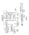
- FIG. 1 An SLDRAM system with which an embodiment of the present invention may be used is illustrated in FIG. 1 .
- the system includes a plurality of SLDRAM modules 11a,..., 11n, which are accessed and controlled by a memory controller 13.
- the memory controller 13 provides a command link to each of the SLDRAM modules 11a,..., 11n, which includes a clock signal CCLK on inverted and non-inverted clock signal paths, a one bit FLAG signal on a FLAG data path, and a ten bit command bus data path CA0-CA9.
- SLDRAM input/output enabling signals SO, SI are provided from the memory controller 13 in a daisy chain fashion to the SLDRAM modules 11a,..., 11n.
- a bidirectional data bus DQ0-DQ17 is provided between the memory controller 13 and each of the SLDRAM modules 11a,..., 11n, as are bi-directional data clocks DCLK0 and DCLK1.
- the first data clock DCLK0 is used to strobe input/output data into and out of the SLDRAM modules, a process for which the second data clock DCLK signal path is also intermittently used.
- FIG. 2 shows a circuit for deriving various clock signals used in the operation of a memory device.
- External clock signals CCLK and CCLK* which are typically used to latch data into a memory device, are received at terminals 31 and 33 and provided through a buffer 35 to an adjustable delay circuit 37, the output of which feeds the delayed CCLK and CCLK* signals into a tapped delay line 41.
- the tapped delay line 41 has a plurality of taps which provide delayed clock signals 0,..., 15 to multiplexers 43 which are capable of providing selected ones of the clock signals 0,..., 15 to selected ones of the buffers 45.
- the buffers 45 in turn supply respective delayed clock signals CCLK and CCLK* to respective output latches 51 of data paths D0,..., D17 for READ/WRITE data of the memory device.
- the output latches 51 in turn supply read data from a memory array to respective output buffers 53 and output terminals 55 and 57.
- One of the delayed signals from tapped delay line 41 is provided to the multiplexer 43 in a manner in which the signal passes through the multiplexer without being switchable to a selected buffer 45.
- This signal that passes through multiplexer 43 and through buffer 45 is the master clock signal MCLK which is used to time various operations within a memory device.
- Another clock output signal for example, at the beginning of the tapped delay line 41 (tap 0), is also provided as a clock signal which passes straight through the multiplexer 43 and the buffer 45 as an input to an input/output model circuit 47.
- the input/output model circuit 47 is a circuit which is designed to provide a specific delay to the signals CCLK and CCLK* through the adjustable delay circuit 37 in accordance with designed operating parameters of the memory device and in response to changes in operating voltage and/or temperature of the device.
- the output of the phase detector 49 is used to adjust the delay circuit 37 to adjust the timing of the applied clock signal CCLK in accordance with voltage and temperature variations experienced by the memory device.
- FIG. 2 also illustrates a phase detector 39 which is used to adjust the length of the tapped delay line 41 such that it remains at a constant length, such as one clock cycle.
- the phase detector 39 operates by comparing the output to the input of the tapped delay line 41 and making the necessary adjustments thereto to ensure that the delay length remains stable.
- the adjustable delay circuit 37 causes timing adjustments in the input signal to the tapped delay line 41, which in turn cause like timing adjustments in the master clock signal MCLK.
- FIG. 3 illustrates an exemplary portion of a memory device circuit for capturing data and expanding the capture data envelope in accordance with all exemplary embodiment of the invention.
- the circuit receives the capture clock signal CCLK, the command bits CA ⁇ 0:9>, a flag signal FLAG and a reset signal RESET as inputs.
- the flag signal FLAG is received to signify the start of a command packet.
- a command packet consists of four command packet words each of which consists of command bits CA ⁇ 0: 9 > , that is, each of the CA0,..., CA9 data paths receives a four-bit data burst for command transfer to the memory device.
- the capture clock signal CCLK is input in to a clock delay circuit 102.
- the clock delay circuit 102 outputs a delayed clock signal CLKD.
- the command bits CA ⁇ 0: 9 > are input into respective command delay circuits 104a,..., 104J (collectively referred to herein as "command delay circuits 104"). It should be noted that there are ten command delay circuits 104 for the command data paths CA0,..., CA9, but only two are illustrated for clarity purposes.
- the outputs of the command delay circuits are delayed command signals CADEL ⁇ 0:9>.
- the flag signal FLAG is input in to a flag delay circuit 106.
- the flag delay circuit 106 outputs a delayed flag signal FDEL.
- the delay circuits 102, 104, 106 are ring delay circuits. Exemplary ring delay circuits and their operation are described in U.S. Patent Application No. 09/201,519, filed on November 30,1998 , entitled “Method and Apparatus for High Speed Data Capture Utilizing Bit-to-Bit Timing Correction, and Memory Device Using the Same,".
- the ring delay circuits consist of a plurality of delay circuits connected as a ring having an output with an adjustable delay (depending upon where the data is input into the ring, i. e., the "insertion point").
- an initial insertion point of the ring delay circuit is chosen and a calibration pattern is sent down a data path.
- An output of the ring delay circuit is sampled to determine if the calibration pattern has been properly captured and to determine its timing. All of the possible insertion points (i.
- a memory device control circuit determines the best delay value for the ring delay circuit and sets the ring delay circuit to this value.
- the best delay typically corresponds to a data envelope centered about the delayed clock signal CLKD.
- a select signal generator 114 receives the delayed clock signal CLKD and the reset signal RESET.
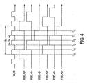
- the select signal generator 114 outputs three rising select signals RSEL ⁇ 0:2> and three falling select signals FSEL ⁇ 0:2>. Referring to FIG. 4 , it can be seen that the select signal generator 114 generates the first rising select signal RSEL ⁇ 0> off the falling edge of CLKD such that RSEL ⁇ 0> corresponds to and centers on the first rising edge of the delayed clock signal CLKD at time t0. Similarly, the select signal generator 114 generates the second and third rising select signals RSEL ⁇ 1:2> centered at times t2 and t4, which correspond to the second and third rising edges of the delayed clock signal CLKD.
- the select signal generator 114 generates the three falling select signals FSEL ⁇ 0> centered at times t1, t3 and t5, which respectively correspond to the first, second and third falling edges of the delayed clock signal CLKD.
- the rising and falling select signals RSEL ⁇ 0:2>, FSEL ⁇ 0:2> enable one of the registers of command latch circuitry so that the delayed clock signal CLKD can latch the data on the input to the corresponding register.
- the circuit contains ten command latch circuits 110a,..., 110J (collectively referred to herein as the "command latch circuits 110"). It should be noted that there are ten command latch circuits 110, but only two are illustrated for clarity purposes.
- the command latch circuits 110 respectively receive the delayed command signals CADEL ⁇ 0:9>, delayed clock signal CLKD, and the rising and falling select signals RSEL ⁇ 0:2>, FSEL ⁇ 0:2>.
- the command latch circuits 110 contain three latched rising edge command outputs CAOR ⁇ 0:2>,..., CA9R ⁇ 0:2> and three latched falling edge command outputs CAOF ⁇ 0:2>,..., CA9F ⁇ 0:2>.
- each command latch circuit 110 contains six latches and six possible outputs. Thus, each command latch circuit 110 may have three latched rising edge command signals and three latched falling edge command signals in certain circumstances.
- the circuit also contains one flag latch circuit 112.
- the flag latch circuit 112 receives the delayed flag signal FDEL, delayed clock signal CLKD, and the rising and falling select signals RSEL ⁇ 0:2>, FSEL ⁇ 0:2>.
- the flag latch circuit 112 contains three latched rising edge flag outputs FLAGR ⁇ 0:2>, three latched falling edge flag outputs FLAGF ⁇ 0:2> and three latched dummy flag outputs DUMBFLAG ⁇ 0:2>. Referring to FIG. 8 , the three latched dummy flag outputs DUMBFLAG ⁇ 0:2> are latched by the flag latch circuit 112 such that they have a data envelope that spans three full clock cycles (i. e., six clock ticks).
- the three latched dummy flag outputs DUMBFLAG ⁇ 0:2> simulate the desired data envelope for the captured data (although the proper timing has yet to be determined).
- the three latched dummy flag outputs DUMBFLAG ⁇ 0:2> are skewed from each other by one full clock cycle.
- the latched dummy flag outputs DUMBFLAG ⁇ 0:2> will be used to synchronize the capture clock latching circuitry to the master clock latching circuitry.
- the latched rising edge command outputs CA0R ⁇ 0:2>,..., CA9R ⁇ 0:2> and latched falling edge command outputs CA0F ⁇ 0:2>,..., CA9F ⁇ 0:2> will be used by a data generator circuitry to transfer the captured information to the master clock domain by increasing the capture data envelope to three clock cycles (i. e., six clock ticks) to ensure that an internally generated master clock edge remains within the data envelope over the entire operating range.
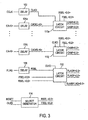
- FIG. 5 is a circuit diagram illustrating an exemplary portion of synchronization and re-timing circuitry constructed in accordance with an exemplary embodiment of the invention.
- the circuitry includes a reset circuit 120 and a selection circuit 130 that synchronize the capture circuitry clocked by the delayed capture clock signal CLKD (illustrated in FIG. 3 ) to the circuitry clocked by the master clock signal MCLK.
- a data generator 140 transfers the captured commands with the expanded data envelope, i.e., latched rising edge command outputs CA0R ⁇ 0:2>,..., CA9R ⁇ 0:2> and latched falling edge command outputs CA0F ⁇ 0:2>,..., CA9F ⁇ 0:2>, to the master clock domain.
- the reset circuit 120 receives the master clock signal MCLK and the latched dummy flag outputs DUMBFLAG ⁇ 0:2> as inputs.
- the flag latch circuit 112 ( FIG. 3 ) generates the three latched dummy flag outputs DUMBFLAG ⁇ 0:2> that simulate the desired capture data envelope (i. e., three full clock cycles). As will be described below, the flag latch circuit 112 ( FIG.
- the reset circuit 120 monitors the three latched dummy flag outputs DUMBFLAG ⁇ 0:2> and issues a reset request signal REQUEST to the selection circuit 130.
- the reset request signal REQUEST is generated by the reset circuit 120 when an edge of the master clock signal MCLK is simultaneously within the data envelopes of all three latched dummy flag outputs DUMBFLAG ⁇ 0:2>.
- the reset request signal REQUEST is output to the selection circuit 130.
- the selection circuit 130 includes two counters 132, 134 that respectively generate three rising edge select signals SELECTR ⁇ 0:2> and three falling edge select signals SELECTF ⁇ 0:2> that are clocked by the master clock signal MCLK.
- the selection circuit 130 also includes a disable circuit 136 that sends an acknowledgment signal ACKNOWLEDGE to the reset circuit 120.
- the reset circuit 120 uses the acknowledgment signal ACKNOWLEDGE to prevent the generation of subsequent reset request signals REQUEST (i. e., the reset circuit 120 is disabled).
- the reset circuit 120 is disabled at this point because the timing between the master clock signal MCLK and the capture data envelope has been established (described below in more detail).
- the three rising edge select signals SELECTR ⁇ 0:2> and three falling edge select signals SELECTF ⁇ 0:2> are output to the data generator 140 so that captured command data (i. e., the latched rising edge command outputs CA0R ⁇ 0:2>,..., CA9R ⁇ 0:2> and the latched falling edge command outputs CA0F ⁇ 0:2>,..., CA9F ⁇ 0:2>) can be transferred to the master clock domain.
- the master clock signal MCLK will be synchronized with the capture data envelope that was clocked by the delayed capture clock signal CLKD. Once synchronized and after the reset circuit 120 is disabled, when command and other information is captured by the capture clock signal CLKD the information will remain valid for three full clock cycles, which ensures that it can be transferred to the master clock domain.
- FIG. 6 is a circuit diagram illustrating an exemplary data generator circuit 140.
- the data generator 140 receives the latched rising edge command outputs CA0R ⁇ 0:2>,..., CA9R ⁇ 0:2>, latched falling edge command outputs CA0F ⁇ 0:2>,..., CA9F ⁇ 0:2>, rising edge select signals SELECTR ⁇ 0:2>, falling edge select signals SELECTF ⁇ 0:2>, latched rising edge flag outputs FLAGR ⁇ 0:2> and the latched falling edge FLAG outputs FLAGF ⁇ 0:2>. It should be noted that only the first latched rising and falling edge command outputs CA0R ⁇ 0:2>, CA0F ⁇ 0:2> are illustrated for clarity purposes.
- circuitry e. g., multiplexers 142, 144 and registers 150, 152, 154, 156) connected to the first latched rising and falling edge command outputs CA0R ⁇ 0:2>, CA0F ⁇ 0:2> is repeated for every command output, but they are not illustrated for clarity purposes.
- the latched rising edge command outputs CA0R ⁇ 0:2> and the rising edge select signals SELECTR ⁇ 0:2> are input into a first command bit multiplexer 142.
- the latched falling edge command outputs CAOF ⁇ 0:2> and the falling edge select signals SELECTF ⁇ 0:2> are input into a second command bit multiplexer 144.
- Each command bit multiplexer 142,144 is a three-to-one multiplexer and is controlled by its respective select signals SELECTR ⁇ 0:2>, SELECTF ⁇ 0:2> to output the two latched command bits (from the same command packet) contained within its respective latched command outputs CA0R ⁇ 0:2>, CA0F ⁇ 0:2>.
- the outputs of the first command bit multiplexer 142 are sent to the first and third registers 150, 154.
- the outputs of the second command bit multiplexer 144 are sent to the second and fourth registers 152, 156.
- the first register 150 is clocked by a first master clock flag signal F ⁇ 0> and outputs a first command bit output YCAO ⁇ 0>.
- the first command bit output YCAO ⁇ 0> represents the first captured command bit CA ⁇ 0> from the first packet word of a command packet that has now been transferred into the master clock domain.
- the second register 152 is clocked by a second master clock flag signal F ⁇ 1> and outputs a second command bit output YCA1 ⁇ 0>.
- the second command bit output YCA1 ⁇ 0> represents the first captured command bit CA ⁇ 0> from the second packet word of a command packet that has now been transferred into the master clock domain.
- the third register 154 is clocked by a third master clock flag signal F ⁇ 2> and outputs a third command bit output YCA2 ⁇ 0>.
- the third command bit output YCA2 ⁇ 0> represents the first captured command bit CA ⁇ 0> from the third packet word of a command packet that has now been transferred into the master clock domain.
- the fourth register 156 is clocked by a fourth master clock flag signal F ⁇ 3> and outputs a fourth command bit output YCA3 ⁇ 0>.
- the fourth command bit output YCA3 ⁇ 0> represents the first captured command bit CA ⁇ 0> from the fourth packet word of a command packet that has now been transferred into the master clock domain.
- the generation of the master clock flag signals F ⁇ 0>, F ⁇ 1>, F ⁇ 2>, F ⁇ 3> is now described.
- the latched rising edge flag outputs FLAGR ⁇ 0:2> and the rising edge select signals SELECTR ⁇ 0:2> are input into a first flag multiplexer 146.
- the latched falling edge FLAG outputs FLAGF ⁇ 0:2> and the falling edge select signals SELECTF ⁇ 0:2> are input into a second flag multiplexer 148.
- Each flag multiplexer 146, 148 is a three-to-one multiplexer and is controlled by its respective select signals SELECTR ⁇ 0:2>, SELECTF ⁇ 0:2> to output the two latched flag signals contained within its respective latched flag outputs FLAGR ⁇ 0:2>, FLAGF ⁇ 0:2>.
- the outputs of the two flag multiplexers 146, 148 are input into a sorting circuit 158.
- the sorting circuit 158 which is clocked by the rising and falling edges of the master clock signal MCLK, outputs a first master clock flag signal F ⁇ 0> .
- the first master clock signal F ⁇ 0> is fed into a first dual edge register 159a, which outputs the second master clock signal F ⁇ 1>.
- the second master clock signal F ⁇ 1> is fed into a second dual edge register 159b, which outputs the third master clock signal F ⁇ 2>.
- the third master clock signal F ⁇ 2> is fed into a third dual edge register 159c, which outputs the fourth master clock signal F ⁇ 3>.
- the master clock flag signals F ⁇ 0>, F ⁇ 1>, F ⁇ 2>, F ⁇ 3> respectively signify the arrival of the four latched command outputs for a single command bit. That is, the first master clock flag signal F ⁇ 0> is used to signify the arrival of the latched command output CAOR ⁇ 0:2> that is associated with the command bit 0 (i.e., CA ⁇ 0>) of the initial captured packet word.
- the second master clock flag signal F ⁇ 1> is used to signify the arrival of the latch command output CA0F ⁇ 0:2> that is associated with the command bit 0 (i. e., CA ⁇ 0>) of the second captured packet word.
- the third master clock flag signal F ⁇ 2> is used to signify the arrival of the latch command output CA0R ⁇ 0:2> that is associated with the command bit 0 (i. e., CA ⁇ 0>) of the third captured packet word.
- the fourth master clock flag signal F ⁇ 3> is used to signify the arrival of the latch command output CA0F ⁇ 0:2> that is associated with the command bit 0 (i. e., CA ⁇ 0>) of the fourth captured packet word.
- the command bit outputs YCA0 ⁇ 0:3>, YCA1 ⁇ 0:3>, YCA2 ⁇ 0:3 >,..., YCA9 ⁇ 0:3> are output from the data generator 140.
- the designation Y ⁇ 0:39> is used to represent the command bit outputs YCA0 ⁇ 0:3>, YCA1 ⁇ 0:3>, YCA2 ⁇ 0:3>,..., YCA9 ⁇ 0:3> .
- the data generator 140 can also output the four master clock flag signals F ⁇ 0:3>. This is represented on FIG. 5 as the output labelled FY ⁇ 0:3>.
- the circuitry described above with respect to FIGS. 1-3 , and 5-6 increases the capture data envelope by two full clock cycles such that captured data remains valid for three full clock cycles (i.e., has a data envelope of three clock cycles or six clock ticks).
- the expanded valid data operating range, now 6 ⁇ radians as opposed to 2 ⁇ radians, is large enough to ensure that a particular edge of the master clock signal MCLK remains within the data envelope over the entire operating range. This way, captured data remains valid and can be properly transferred to the master clock domain from the capture clock domain despite temperature and voltage variations that may effect the timing of the memory device.
- FIGS. 7 and 8 the manner in which the master clock signal MCLK is centered within the middle 2 ⁇ radians of the 6 ⁇ radians data eye is now described (i.e., the manner in which the relationship between the delayed capture clock signal CLKD and the master clock signal MCLK is established and maintained).
- the 6 ⁇ radians data envelope for latched falling edge command outputs CA0F ⁇ 0>,..., CA9F ⁇ 0> is illustrated along with the capture clock signal CLKD, master clock signal MCLK and the first falling edge select signal SELECTF ⁇ 0>.
- FIG. 7 the 6 ⁇ radians data envelope for latched falling edge command outputs CA0F ⁇ 0>,..., CA9F ⁇ 0> is illustrated along with the capture clock signal CLKD, master clock signal MCLK and the first falling edge select signal SELECTF ⁇ 0>.
- the reset request signal REQUEST is de-asserted by the acknowledgement signal ACKNOWLEDGE.
- the rising edge counter 132 FIG. 5
- the falling edge counter 134 FIG. 5
- the reset request signal REQUEST is de-asserted before this falling edge (i.e., arrow C) of the master clock signal MCLK.
- the rising edge counter 132 ( FIG. 5 ) begins to count.
- the same MCLK edge clocks in the latched rising edge command output CAOR ⁇ 0> since the first command bit multiplexer 142 is open, the same MCLK edge clocks in the latched rising edge command output CAOR ⁇ 0>. It should be noted that the same operations occur for the falling edge command outputs CA0F ⁇ 0>,..., CA9F ⁇ 0> on the falling edges of the MCLK signal ( FIG. 7 ). This is made possible by the use of the latched dummy flag outputs DUMBFLAG ⁇ 0:2> by the reset circuit 120 ( FIG. 5 ).
- the reset circuit 120 can establish when the rising select signal RSEL ⁇ 0> is present at the latch circuits 110, 112.
- the rising select signal RSEL ⁇ 0> is selecting the proper rising edge register within the latch circuit 110 at which point, the first command bit multiplexer 142 should be opened to accept the latched rising edge command output CAOR ⁇ 0> from the latch circuit 110 in accordance with the master clock signal MCLK.
- the embodiment of the present invention wants to ensure that the inputs to the first command bit multiplexer 142 (as well as the other multiplexers in the data generator 140) open at the right time relative the timing of the outputs of the latch circuits 110.
- the SELECTR ⁇ 1> goes high at the same time the rising edge command output CAOR ⁇ 0> is clocked into the command bit multiplexer 142 by the master clock signal MCLK.
- the master clock signal MCLK and the delayed capture clock signal CLKD are synchronized.
- the clock edge labelled R0 is the edge that places the edge of the master clock signal MCLK within the middle 2 ⁇ radians of the 6 ⁇ radians data eye.
- the relationship between the master clock signal MCLK and the capture clock signal CLKD is maintained since the data eye is stretched to compensate for variations in the temperature and voltage of the memory device.
- the 6 ⁇ radian envelope described herein allows for up to ⁇ 2 ⁇ radians of clock phase variation due to temperature and voltage.
- the relationship is illustrated in FIG. 7 by the mapping of the edge labelled RO of the capture clock signal CLKD to the R0 edge of the master clock signal MCLK.
- FIG. 9 is a circuit diagram illustrating an exemplary command latch circuit 110 constructed in accordance with an exemplary embodiment of the invention.
- the latch circuit 110 includes six registers 200, 202, 204, 206, 208, 210. Although registers are illustrated in FIG. 9 , it should be noted that any type of latching circuitry, e.g., latch, flip-flop, etc., can be used as long as the latching circuitry provides the latching capabilities described below.
- the first three registers 200, 202, 204 are clocked by the delayed clock signal CLKD.
- the first register 200 receives the first rising select signal RSEL ⁇ 0>
- the second register 202 receives the second rising select signal RSEL ⁇ 1>
- the third register 204 receives the third rising select signal RSEL ⁇ 2>.
- the last three registers 206, 208, 210 are clocked by the inverse of the delayed clock signal CLKD .
- the fourth register 206 receives the first falling select signal FSEL ⁇ 0>
- the fifth register 208 receives the second falling select signal FSEL ⁇ 1>
- the sixth register 210 receives the third falling select signal FSEL ⁇ 2>.
- All of the registers receive the delayed command signals CADEL ⁇ 0> as a second input. It should be noted that since there will be ten latch circuits 110, each latch circuit 110 will input a different delayed command signal, but for purposes of this discussion, it is presumed that the circuit 110 inputs the first delayed command signal CADEL ⁇ 0>.
- the registers 200, 202, 204, 206, 208, 210 output the three latched rising edge command outputs CAOR ⁇ 0:2> and the three latched falling edge command outputs CAOF ⁇ 0:2>.
- FIG. 10 is a circuit diagram illustrating an exemplary flag latch circuit 112 constructed in accordance with an exemplary embodiment of the invention.
- the latch circuit 112 includes nine registers 220, 222, 224, 226, 228, 230, 232, 234, 236. Although registers are illustrated in FIG. 10 , it should be noted that any type of latching circuitry, e. g., latch, flip-flop, etc., can be used as long as the latching circuitry provides the latching capabilities described below.
- the first three and last three registers 220, 222, 224, 232, 234, 236 are clocked by the delayed clock signal CLKD.
- the first register 220 receives the first rising select signal RSEL ⁇ 0>
- the second register 222 receives the second rising select signal RSEL ⁇ 1>
- the third register 224 receives the third rising select signal RSEL ⁇ 2>.
- the middle three registers 226, 228, 230 are clocked by the inverse of the delayed clock signal CLKD .
- the fourth register 226 receives the first falling select signal FSEL ⁇ 0>
- the fifth register 228 receives the second falling select signal FSEL ⁇ 1>
- the sixth register 230 receives the third falling select signal FSEL ⁇ 2>.
- the seventh register 232 receives the first rising select' signal RSEL ⁇ 0>
- the eighth register 234 receives the second rising select signal RSEL ⁇ 1>
- the ninth register 236 receives the third rising select signal RSEL ⁇ 2>.
- the last three registers 232, 234, 236 are connected as a toggle circuit. That is, the output of the seventh register 232 is input back into the seventh register 232 after it is inverted by an inverter 240.
- the output of the seventh register 232 is also input into the eighth register 234 and the output of the eighth register 234 is input into the ninth register 236. As described above with respect to FIG.
- the last three registers 232, 234, 236 generate the three latched dummy flag outputs DUMBFLAG ⁇ 0:2> by toggling data bits between a logic "1" and "0" through their respective inputs (as clocked by the delayed clock CLKD and selected by the rising select signals RSEL ⁇ 0:2>).
- the dummy flag outputs DUMBFLAG ⁇ 0:2> are used to synchronize the circuitry operating under the delayed capture data clock signal CLKD to the circuitry operating under the master clock signal MCLK.
- the first six registers 220, 222, 224, 226, 228, 230 receive the delayed flag signal FDEL as a second input.
- the registers 220, 222, 224, 226, 228, 230 output the three latched rising edge flag outputs FLAGR ⁇ 0:2> and the three latched falling edge flag outputs FLAGF ⁇ 0:2>.
- These latched flag outputs FLAGR ⁇ 0:2>, FLAGF ⁇ 0:2> are used by the data generator 140 to assemble and output captured command data using the master clock signal MCLK (illustrated in FIGS. 5 and 6 ).
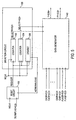
- a memory device containing the synchronization scheme described above may be used in a processor-based system 300 of the type shown in FIG. 11 .
- the processor-based system 300 comprises a processor 302 that communicates with a memory device 312 and an I/O device 308 over a bus 320.
- the bus 320 may be a series of buses and bridges commonly used in a processor based system, but for convenience purposes only, the bus 320 has been illustrated as a single bus.
- the memory device 312 contains the synchronizing circuitry of the embodiment of the present invention.
- the memory device 312 may be any type of DRAM device including an SLDRAM.
- the processor 302 may itself be an integrated processor which utilizes on-chip memory devices containing the synchronizing circuitry of the embodiment of the present invention.
- the processor-based system 300 may be a computer system, a process control system or any other system employing a processor and associated memory.
- a second I/O device 310 is illustrated, but is not necessary to practice the invention.
- the processor-based system 300 may also include read-only memory (ROM) 314 and may include peripheral devices such as a floppy disk drive 304 and a compact disk (CD) ROM drive 306 that also communicate with the processor 302 over the bus 320 as is well known in the art.
- ROM read-only memory
- CD compact disk
- One aspect of the invention provides a memory device comprising: a plurality of first circuits, each first circuit having a first input for receiving a first clock signal and a second input for receiving a respective first input signal, each first circuit being controllable to latch its respective first input signal such that the first input signal has a data envelope corresponding to N number of cycles of the first clock signal, where N > 1, each first circuit having at least one first output signal corresponding to the latched first input signal; and a re-timing circuit coupled to said plurality of first circuits, said re-timing circuit having a third input for receiving a second clock signal, said re-timing circuit receiving said at least one first output signal from said first circuits and outputting re-timed first output signals in accordance with transitions of the second clock signal.
- each first circuit has two first output signals, a first one of said first output signals corresponding to the latched first input signal associated with a first edge of the first clock signal and a second one of said first output signals corresponding to the latched first input signal associated with a second edge of the first clock signal.
- said re-timing circuit receives said two first output signals from each of said first circuits and combines said first output signals into said re-timed first output signals.
- the memory device further comprises a second circuit having a fourth input for receiving the first clock signal and a fifth input for receiving a second input signal, said second circuit being controllable to latch the second input signal such that the second input signal has a data envelope corresponding to N number of cycles of the first clock signal, where N > 1, said second circuit having at least one second output signal corresponding to the latched second input signal, wherein said re-timing circuit receives said at least one second output signal from said second circuit and uses said least one second output signal to re-time said first output signals.
- said second circuit has two second output signals, a first one of said second output signals corresponding to the latched second input signal associated with a first edge of the first clock signal and a second one of said second output signals corresponding to the latched second input signal associated with a second edge of the first clock signal.
- said second circuit has three second output signals, a first one of said second output signals corresponding to the latched second input signal associated with a first edge of the first clock signal, a second one of said second output signals corresponding to the latched second input signal associated with a second edge of the first clock signal and a third one of said second output signals corresponding to a synchronization signal associated with the first clock signal.
- said re-timing circuit comprises: a reset circuit for generating a synchronization request signal, said reset circuit coupled to said third one of said second output signals and the second clock signal, said reset circuit outputting said synchronization request signal based on said third one of said second output signals; a selection circuit for generating at least one selection signal responsive to said synchronization request signal; and a data generator receiving said at least one selection signal and said first and second output signals and generating said re-timed first output signals responsive to said at least one selection signal.
- said data generator generates and outputs a re-timed first one of said second output signals and a retimed second one of said second output signals.
- N is three.
- the first clock signal is received through a delay element and the second clock signal is generated based on said first clock signal.
- all of said latched first input signals remains valid for a period sufficiently long enough so that said re-timing circuit can output said re-timed first output signals regardless of voltage variations effecting a timing of said first circuits and said re-timing circuits.
- all of said latched first input signals remain valid for a period sufficiently long enough so that said re-timing circuit can output said re-timed first output signals regardless of temperature variations effecting a timing of said first circuits and said re-timing circuits.
- One aspect of the invention provides a method of operating a memory device, said method comprising the steps of : receiving a plurality of first input signals responsive to a first clock signal; latching the received first input signals such that each latched input signal has a data envelope corresponding to N number of cycles of the first clock signal, where N > 1; and outputting re-timed first input signals in accordance with transitions of a second clock signal, wherein the data envelope of each latched first input signal ensures that the latched first input signals are valid when re-timed.
- said latching step comprises: latching a first portion of the first input signals to a first edge of the first clock signal; and latching a second portion of the first input signals to a second edge of the first clock signal.
- said re-timing step comprises: receiving said latched first and second portions; and combining said first and second portions in accordance with transitions of the second clock signal.
- the method further comprises the steps of: receiving a second input signal; and latching the second input signal such that the second input signal has a data envelope corresponding to N number of cycles of the first clock signal, where N > 1, wherein said re-timing step receives the latched second input and uses it re-time the first input signals.
- the method further comprises the steps of: generating synchronization signals simulating a timing of the first input signals; and synchronizing circuitry responsible for capturing the first input signals to circuitry responsible for outputting the re-timed first input signals.
- said synchronizing step comprises: generating a synchronization request signal based on said synchronization signals; generating at least one selection signal responsive to said synchronization request signal; and generating the re-timed first input signals responsive to the at least one selection signal.
- N is three.
- all of the latched first input signals remains valid for a period sufficiently long enough so that said re-timing step circuit can output the re-timed first input signals regardless of voltage variations effecting a timing of the memory device.
- all of the latched first input signals remains valid for a period sufficiently long enough so that said re-timing step circuit can output the re-timed first input signals regardless of temperature variations effecting a timing of the memory device.
- the invention provides a processor system comprising a processor and the memory device as defined above.
Landscapes
- Engineering & Computer Science (AREA)
- Microelectronics & Electronic Packaging (AREA)
- Computer Hardware Design (AREA)
- Dram (AREA)
- Measurement Of Velocity Or Position Using Acoustic Or Ultrasonic Waves (AREA)
- Synchronisation In Digital Transmission Systems (AREA)
Applications Claiming Priority (2)
| Application Number | Priority Date | Filing Date | Title |
|---|---|---|---|
| US09/642,090 US6333893B1 (en) | 2000-08-21 | 2000-08-21 | Method and apparatus for crossing clock domain boundaries |
| EP20010962262 EP1312094B1 (de) | 2000-08-21 | 2001-08-21 | Verfahren und vorrichtung zum durchqueren der grenzen von taktgebieten |
Related Parent Applications (1)
| Application Number | Title | Priority Date | Filing Date |
|---|---|---|---|
| EP01962262.0 Division | 2001-08-21 |
Publications (2)
| Publication Number | Publication Date |
|---|---|
| EP2290657A1 true EP2290657A1 (de) | 2011-03-02 |
| EP2290657B1 EP2290657B1 (de) | 2012-05-09 |
Family
ID=24575155
Family Applications (2)
| Application Number | Title | Priority Date | Filing Date |
|---|---|---|---|
| EP20010962262 Expired - Lifetime EP1312094B1 (de) | 2000-08-21 | 2001-08-21 | Verfahren und vorrichtung zum durchqueren der grenzen von taktgebieten |
| EP10011175A Expired - Lifetime EP2290657B1 (de) | 2000-08-21 | 2001-08-21 | Verfahren und Vorrichtung zum Durchqueren der Grenzen von Taktgebieten |
Family Applications Before (1)
| Application Number | Title | Priority Date | Filing Date |
|---|---|---|---|
| EP20010962262 Expired - Lifetime EP1312094B1 (de) | 2000-08-21 | 2001-08-21 | Verfahren und vorrichtung zum durchqueren der grenzen von taktgebieten |
Country Status (9)
| Country | Link |
|---|---|
| US (2) | US6333893B1 (de) |
| EP (2) | EP1312094B1 (de) |
| JP (1) | JP5138857B2 (de) |
| KR (1) | KR100607773B1 (de) |
| CN (1) | CN1291417C (de) |
| AT (2) | ATE557396T1 (de) |
| AU (1) | AU2001283458A1 (de) |
| DE (1) | DE60143581D1 (de) |
| WO (1) | WO2002017325A1 (de) |
Families Citing this family (36)
| Publication number | Priority date | Publication date | Assignee | Title |
|---|---|---|---|---|
| US6675272B2 (en) | 2001-04-24 | 2004-01-06 | Rambus Inc. | Method and apparatus for coordinating memory operations among diversely-located memory components |
| US7058799B2 (en) * | 2001-06-19 | 2006-06-06 | Micron Technology, Inc. | Apparatus and method for clock domain crossing with integrated decode |
| JP4812976B2 (ja) * | 2001-07-30 | 2011-11-09 | エルピーダメモリ株式会社 | レジスタ、メモリモジュール及びメモリシステム |
| JP2003044349A (ja) * | 2001-07-30 | 2003-02-14 | Elpida Memory Inc | レジスタ及び信号生成方法 |
| US6661554B2 (en) * | 2001-08-23 | 2003-12-09 | Cyoptics (Israel) Ltd. | Biasing of an electro-optical component |
| US6952791B2 (en) * | 2001-12-03 | 2005-10-04 | Broadcom Corporation | Method and circuit for initializing a de-skewing buffer in a clock forwarded system |
| US6774687B2 (en) * | 2002-03-11 | 2004-08-10 | Micron Technology, Inc. | Method and apparatus for characterizing a delay locked loop |
| US6966022B1 (en) * | 2002-04-04 | 2005-11-15 | Adaptec, Inc. | System and method for determining integrated circuit logic speed |
| US7319728B2 (en) | 2002-05-16 | 2008-01-15 | Micron Technology, Inc. | Delay locked loop with frequency control |
| US6900685B2 (en) * | 2002-05-16 | 2005-05-31 | Micron Technology | Tunable delay circuit |
| US6801070B2 (en) | 2002-05-16 | 2004-10-05 | Micron Technology, Inc. | Measure-controlled circuit with frequency control |
| US6983354B2 (en) | 2002-05-24 | 2006-01-03 | Micron Technology, Inc. | Memory device sequencer and method supporting multiple memory device clock speeds |
| US7085905B2 (en) * | 2002-07-18 | 2006-08-01 | Sun Microsystems, Inc. | Memory data stretcher |
| US20040013003A1 (en) * | 2002-07-19 | 2004-01-22 | Micron Technology, Inc. | First bit data eye compensation for open drain output driver |
| US6865135B2 (en) * | 2003-03-12 | 2005-03-08 | Micron Technology, Inc. | Multi-frequency synchronizing clock signal generator |
| US7299329B2 (en) * | 2004-01-29 | 2007-11-20 | Micron Technology, Inc. | Dual edge command in DRAM |
| US7171321B2 (en) | 2004-08-20 | 2007-01-30 | Rambus Inc. | Individual data line strobe-offset control in memory systems |
| US7084680B2 (en) * | 2004-08-31 | 2006-08-01 | Micron Technology, Inc. | Method and apparatus for timing domain crossing |
| US7301831B2 (en) * | 2004-09-15 | 2007-11-27 | Rambus Inc. | Memory systems with variable delays for write data signals |
| US9809278B2 (en) * | 2004-09-28 | 2017-11-07 | Shimano, Inc. | Apparatus for reducing an engaging force of an engaging member |
| US7543172B2 (en) | 2004-12-21 | 2009-06-02 | Rambus Inc. | Strobe masking in a signaling system having multiple clock domains |
| US7688672B2 (en) * | 2005-03-14 | 2010-03-30 | Rambus Inc. | Self-timed interface for strobe-based systems |
| US7526704B2 (en) * | 2005-08-23 | 2009-04-28 | Micron Technology, Inc. | Testing system and method allowing adjustment of signal transmit timing |
| US20080005709A1 (en) * | 2006-06-30 | 2008-01-03 | International Business Machines Corporation | Verification of logic circuits using cycle based delay models |
| US7685542B2 (en) * | 2007-02-09 | 2010-03-23 | International Business Machines Corporation | Method and apparatus for shutting off data capture across asynchronous clock domains during at-speed testing |
| US8108738B2 (en) * | 2007-06-26 | 2012-01-31 | International Business Machines Corporation | Data eye monitor method and apparatus |
| US7779375B2 (en) * | 2007-10-17 | 2010-08-17 | International Business Machines Corporation | Design structure for shutting off data capture across asynchronous clock domains during at-speed testing |
| US7500132B1 (en) * | 2008-04-11 | 2009-03-03 | International Business Machines Corporation | Method of asynchronously transmitting data between clock domains |
| US8132036B2 (en) * | 2008-04-25 | 2012-03-06 | International Business Machines Corporation | Reducing latency in data transfer between asynchronous clock domains |
| US20120110244A1 (en) * | 2010-11-02 | 2012-05-03 | Micron Technology, Inc. | Copyback operations |
| US9008196B2 (en) * | 2011-04-28 | 2015-04-14 | International Business Machines Corporation | Updating interface settings for an interface |
| US9225322B2 (en) | 2013-12-17 | 2015-12-29 | Micron Technology, Inc. | Apparatuses and methods for providing clock signals |
| US8929152B1 (en) | 2014-04-02 | 2015-01-06 | Altera Corporation | Retiming programmable devices incorporating random access memories |
| KR102251813B1 (ko) | 2015-04-07 | 2021-05-13 | 삼성전자주식회사 | 메모리 시스템 및 메모리 시스템의 동작 방법 |
| US10313099B1 (en) * | 2018-06-04 | 2019-06-04 | MACOM Technology Solutions Holding, Inc. | Multi-lane coherent transceiver with synchronized lane reset signals |
| US10999050B1 (en) | 2020-05-04 | 2021-05-04 | Stmicroelectronics International N.V. | Methods and apparatus for data synchronization in systems having multiple clock and reset domains |
Citations (4)
| Publication number | Priority date | Publication date | Assignee | Title |
|---|---|---|---|---|
| JP2000040363A (ja) * | 1998-05-21 | 2000-02-08 | Nec Corp | 半導体記憶装置 |
| US6026050A (en) * | 1997-07-09 | 2000-02-15 | Micron Technology, Inc. | Method and apparatus for adaptively adjusting the timing of a clock signal used to latch digital signals, and memory device using same |
| US6075393A (en) * | 1997-07-22 | 2000-06-13 | Fujitsu Limited | Clock synchronous semiconductor device system and semiconductor devices used with the same |
| US6229757B1 (en) * | 1998-05-21 | 2001-05-08 | Nec Corporation | Semiconductor memory device capable of securing large latch margin |
Family Cites Families (11)
| Publication number | Priority date | Publication date | Assignee | Title |
|---|---|---|---|---|
| US4286255A (en) * | 1979-02-22 | 1981-08-25 | Burroughs Corporation | Signature verification method and apparatus |
| JPS573283A (en) * | 1980-06-03 | 1982-01-08 | Hitachi Denshi Ltd | Readout system for data |
| EP0311448B1 (de) * | 1987-10-09 | 1994-01-19 | Kabushiki Kaisha Toshiba | Digitaler Multiplexer |
| US5487092A (en) | 1994-12-22 | 1996-01-23 | International Business Machines Corporation | System for high-speed synchronization across clock domains |
| JP3612634B2 (ja) * | 1996-07-09 | 2005-01-19 | 富士通株式会社 | 高速クロック信号に対応した入力バッファ回路、集積回路装置、半導体記憶装置、及び集積回路システム |
| US5951635A (en) * | 1996-11-18 | 1999-09-14 | Vlsi Technology, Inc. | Asynchronous FIFO controller |
| US5915107A (en) | 1997-09-26 | 1999-06-22 | Advanced Micro Devices, Inc. | Cross clock domain clocking for a system using two clock frequencies where one frequency is fractional multiple of the other |
| US6000022A (en) | 1997-10-10 | 1999-12-07 | Micron Technology, Inc. | Method and apparatus for coupling signals between two circuits operating in different clock domains |
| JP3859885B2 (ja) * | 1998-11-24 | 2006-12-20 | Necエレクトロニクス株式会社 | 半導体記憶装置 |
| US6430696B1 (en) * | 1998-11-30 | 2002-08-06 | Micron Technology, Inc. | Method and apparatus for high speed data capture utilizing bit-to-bit timing correction, and memory device using same |
| US6081477A (en) * | 1998-12-03 | 2000-06-27 | Micron Technology, Inc. | Write scheme for a double data rate SDRAM |
-
2000
- 2000-08-21 US US09/642,090 patent/US6333893B1/en not_active Expired - Lifetime
-
2001
- 2001-06-21 US US09/884,903 patent/US6414903B1/en not_active Expired - Lifetime
- 2001-08-21 EP EP20010962262 patent/EP1312094B1/de not_active Expired - Lifetime
- 2001-08-21 JP JP2002521303A patent/JP5138857B2/ja not_active Expired - Fee Related
- 2001-08-21 WO PCT/US2001/025955 patent/WO2002017325A1/en not_active Ceased
- 2001-08-21 AT AT10011175T patent/ATE557396T1/de active
- 2001-08-21 KR KR20037002588A patent/KR100607773B1/ko not_active Expired - Fee Related
- 2001-08-21 CN CNB018144276A patent/CN1291417C/zh not_active Expired - Fee Related
- 2001-08-21 AT AT01962262T patent/ATE490539T1/de not_active IP Right Cessation
- 2001-08-21 EP EP10011175A patent/EP2290657B1/de not_active Expired - Lifetime
- 2001-08-21 AU AU2001283458A patent/AU2001283458A1/en not_active Abandoned
- 2001-08-21 DE DE60143581T patent/DE60143581D1/de not_active Expired - Lifetime
Patent Citations (4)
| Publication number | Priority date | Publication date | Assignee | Title |
|---|---|---|---|---|
| US6026050A (en) * | 1997-07-09 | 2000-02-15 | Micron Technology, Inc. | Method and apparatus for adaptively adjusting the timing of a clock signal used to latch digital signals, and memory device using same |
| US6075393A (en) * | 1997-07-22 | 2000-06-13 | Fujitsu Limited | Clock synchronous semiconductor device system and semiconductor devices used with the same |
| JP2000040363A (ja) * | 1998-05-21 | 2000-02-08 | Nec Corp | 半導体記憶装置 |
| US6229757B1 (en) * | 1998-05-21 | 2001-05-08 | Nec Corporation | Semiconductor memory device capable of securing large latch margin |
Non-Patent Citations (1)
| Title |
|---|
| GILLINGHAM: "SLDRAM Consortium", 29 August 1997, article "SLDRAM Architectural and Functional Overview" |
Also Published As
| Publication number | Publication date |
|---|---|
| KR100607773B1 (ko) | 2006-08-01 |
| JP2004507033A (ja) | 2004-03-04 |
| US6333893B1 (en) | 2001-12-25 |
| EP2290657B1 (de) | 2012-05-09 |
| EP1312094A1 (de) | 2003-05-21 |
| KR20030028813A (ko) | 2003-04-10 |
| CN1291417C (zh) | 2006-12-20 |
| EP1312094B1 (de) | 2010-12-01 |
| US6414903B1 (en) | 2002-07-02 |
| CN1447975A (zh) | 2003-10-08 |
| ATE490539T1 (de) | 2010-12-15 |
| US20020021616A1 (en) | 2002-02-21 |
| JP5138857B2 (ja) | 2013-02-06 |
| WO2002017325A1 (en) | 2002-02-28 |
| AU2001283458A1 (en) | 2002-03-04 |
| DE60143581D1 (de) | 2011-01-13 |
| ATE557396T1 (de) | 2012-05-15 |
Similar Documents
| Publication | Publication Date | Title |
|---|---|---|
| EP1312094B1 (de) | Verfahren und vorrichtung zum durchqueren der grenzen von taktgebieten | |
| US10679683B1 (en) | Timing circuit for command path in a memory device | |
| KR100822001B1 (ko) | 반도체기억장치 및 반도체기억회로의 동작방법 | |
| US7675791B2 (en) | Synchronous memory device | |
| US6801989B2 (en) | Method and system for adjusting the timing offset between a clock signal and respective digital signals transmitted along with that clock signal, and memory device and computer system using same | |
| US7415404B2 (en) | Method and apparatus for generating a sequence of clock signals | |
| US6477107B1 (en) | Integrated circuit memory devices having data selection circuits therein which are compatible with single and dual data rate mode operation and methods of operating same | |
| JP4787988B2 (ja) | ダブルデータレートダイナミックランダムアクセスメモリ用出力回路、及びダブルデータレートダイナミックランダムアクセスメモリ | |
| US20060066375A1 (en) | Delay line synchronizer apparatus and method | |
| US10636463B2 (en) | Techniques for command synchronization in a memory device | |
| US6982924B2 (en) | Data output control circuit | |
| US11146275B2 (en) | Signal generation circuit and a semiconductor apparatus using the signal generation circuit | |
| CN101276642A (zh) | 用于控制高速存储器的读取等待时间的方法和装置 | |
| US6920080B2 (en) | Methods for generating output control signals in synchronous semiconductor memory devices and related semiconductor memory devices | |
| US12073914B2 (en) | Memory device, a memory system and an operating method of the memory device | |
| US7385861B1 (en) | Synchronization circuit for DDR IO interface | |
| CN108038068B (zh) | 一种基于ddr读数据同步方法及系统 | |
| JP4027709B2 (ja) | 半導体メモリ装置の入力回路 | |
| CN118399932A (zh) | 一种延时产生电路及其方法、存储器 |
Legal Events
| Date | Code | Title | Description |
|---|---|---|---|
| PUAI | Public reference made under article 153(3) epc to a published international application that has entered the european phase |
Free format text: ORIGINAL CODE: 0009012 |
|
| 17P | Request for examination filed |
Effective date: 20101020 |
|
| AC | Divisional application: reference to earlier application |
Ref document number: 1312094 Country of ref document: EP Kind code of ref document: P |
|
| AK | Designated contracting states |
Kind code of ref document: A1 Designated state(s): AT BE CH CY DE DK ES FI FR GB GR IE IT LI LU MC NL PT SE TR |
|
| GRAP | Despatch of communication of intention to grant a patent |
Free format text: ORIGINAL CODE: EPIDOSNIGR1 |
|
| GRAS | Grant fee paid |
Free format text: ORIGINAL CODE: EPIDOSNIGR3 |
|
| GRAA | (expected) grant |
Free format text: ORIGINAL CODE: 0009210 |
|
| AC | Divisional application: reference to earlier application |
Ref document number: 1312094 Country of ref document: EP Kind code of ref document: P |
|
| AK | Designated contracting states |
Kind code of ref document: B1 Designated state(s): AT BE CH CY DE DK ES FI FR GB GR IE IT LI LU MC NL PT SE TR |
|
| REG | Reference to a national code |
Ref country code: GB Ref legal event code: FG4D |
|
| REG | Reference to a national code |
Ref country code: AT Ref legal event code: REF Ref document number: 557396 Country of ref document: AT Kind code of ref document: T Effective date: 20120515 Ref country code: CH Ref legal event code: EP |
|
| REG | Reference to a national code |
Ref country code: IE Ref legal event code: FG4D |
|
| REG | Reference to a national code |
Ref country code: DE Ref legal event code: R096 Ref document number: 60146562 Country of ref document: DE Effective date: 20120705 |
|
| REG | Reference to a national code |
Ref country code: NL Ref legal event code: VDEP Effective date: 20120509 |
|
| PG25 | Lapsed in a contracting state [announced via postgrant information from national office to epo] |
Ref country code: CY Free format text: LAPSE BECAUSE OF FAILURE TO SUBMIT A TRANSLATION OF THE DESCRIPTION OR TO PAY THE FEE WITHIN THE PRESCRIBED TIME-LIMIT Effective date: 20120509 Ref country code: SE Free format text: LAPSE BECAUSE OF FAILURE TO SUBMIT A TRANSLATION OF THE DESCRIPTION OR TO PAY THE FEE WITHIN THE PRESCRIBED TIME-LIMIT Effective date: 20120509 Ref country code: FI Free format text: LAPSE BECAUSE OF FAILURE TO SUBMIT A TRANSLATION OF THE DESCRIPTION OR TO PAY THE FEE WITHIN THE PRESCRIBED TIME-LIMIT Effective date: 20120509 |
|
| REG | Reference to a national code |
Ref country code: AT Ref legal event code: MK05 Ref document number: 557396 Country of ref document: AT Kind code of ref document: T Effective date: 20120509 |
|
| PG25 | Lapsed in a contracting state [announced via postgrant information from national office to epo] |
Ref country code: GR Free format text: LAPSE BECAUSE OF FAILURE TO SUBMIT A TRANSLATION OF THE DESCRIPTION OR TO PAY THE FEE WITHIN THE PRESCRIBED TIME-LIMIT Effective date: 20120810 Ref country code: PT Free format text: LAPSE BECAUSE OF FAILURE TO SUBMIT A TRANSLATION OF THE DESCRIPTION OR TO PAY THE FEE WITHIN THE PRESCRIBED TIME-LIMIT Effective date: 20120910 |
|
| PG25 | Lapsed in a contracting state [announced via postgrant information from national office to epo] |
Ref country code: BE Free format text: LAPSE BECAUSE OF FAILURE TO SUBMIT A TRANSLATION OF THE DESCRIPTION OR TO PAY THE FEE WITHIN THE PRESCRIBED TIME-LIMIT Effective date: 20120509 |
|
| PG25 | Lapsed in a contracting state [announced via postgrant information from national office to epo] |
Ref country code: NL Free format text: LAPSE BECAUSE OF FAILURE TO SUBMIT A TRANSLATION OF THE DESCRIPTION OR TO PAY THE FEE WITHIN THE PRESCRIBED TIME-LIMIT Effective date: 20120509 Ref country code: DK Free format text: LAPSE BECAUSE OF FAILURE TO SUBMIT A TRANSLATION OF THE DESCRIPTION OR TO PAY THE FEE WITHIN THE PRESCRIBED TIME-LIMIT Effective date: 20120509 Ref country code: AT Free format text: LAPSE BECAUSE OF FAILURE TO SUBMIT A TRANSLATION OF THE DESCRIPTION OR TO PAY THE FEE WITHIN THE PRESCRIBED TIME-LIMIT Effective date: 20120509 |
|
| PG25 | Lapsed in a contracting state [announced via postgrant information from national office to epo] |
Ref country code: IT Free format text: LAPSE BECAUSE OF FAILURE TO SUBMIT A TRANSLATION OF THE DESCRIPTION OR TO PAY THE FEE WITHIN THE PRESCRIBED TIME-LIMIT Effective date: 20120509 |
|
| PLBE | No opposition filed within time limit |
Free format text: ORIGINAL CODE: 0009261 |
|
| STAA | Information on the status of an ep patent application or granted ep patent |
Free format text: STATUS: NO OPPOSITION FILED WITHIN TIME LIMIT |
|
| REG | Reference to a national code |
Ref country code: CH Ref legal event code: PL |
|
| PG25 | Lapsed in a contracting state [announced via postgrant information from national office to epo] |
Ref country code: MC Free format text: LAPSE BECAUSE OF NON-PAYMENT OF DUE FEES Effective date: 20120831 |
|
| 26N | No opposition filed |
Effective date: 20130212 |
|
| PG25 | Lapsed in a contracting state [announced via postgrant information from national office to epo] |
Ref country code: CH Free format text: LAPSE BECAUSE OF NON-PAYMENT OF DUE FEES Effective date: 20120831 Ref country code: ES Free format text: LAPSE BECAUSE OF FAILURE TO SUBMIT A TRANSLATION OF THE DESCRIPTION OR TO PAY THE FEE WITHIN THE PRESCRIBED TIME-LIMIT Effective date: 20120820 Ref country code: LI Free format text: LAPSE BECAUSE OF NON-PAYMENT OF DUE FEES Effective date: 20120831 |
|
| REG | Reference to a national code |
Ref country code: IE Ref legal event code: MM4A |
|
| REG | Reference to a national code |
Ref country code: DE Ref legal event code: R097 Ref document number: 60146562 Country of ref document: DE Effective date: 20130212 |
|
| PG25 | Lapsed in a contracting state [announced via postgrant information from national office to epo] |
Ref country code: IE Free format text: LAPSE BECAUSE OF NON-PAYMENT OF DUE FEES Effective date: 20120821 |
|
| PG25 | Lapsed in a contracting state [announced via postgrant information from national office to epo] |
Ref country code: TR Free format text: LAPSE BECAUSE OF FAILURE TO SUBMIT A TRANSLATION OF THE DESCRIPTION OR TO PAY THE FEE WITHIN THE PRESCRIBED TIME-LIMIT Effective date: 20120509 |
|
| PG25 | Lapsed in a contracting state [announced via postgrant information from national office to epo] |
Ref country code: LU Free format text: LAPSE BECAUSE OF NON-PAYMENT OF DUE FEES Effective date: 20120821 |
|
| PGFP | Annual fee paid to national office [announced via postgrant information from national office to epo] |
Ref country code: DE Payment date: 20140813 Year of fee payment: 14 |
|
| PGFP | Annual fee paid to national office [announced via postgrant information from national office to epo] |
Ref country code: GB Payment date: 20140820 Year of fee payment: 14 Ref country code: FR Payment date: 20140808 Year of fee payment: 14 |
|
| REG | Reference to a national code |
Ref country code: DE Ref legal event code: R119 Ref document number: 60146562 Country of ref document: DE |
|
| GBPC | Gb: european patent ceased through non-payment of renewal fee |
Effective date: 20150821 |
|
| REG | Reference to a national code |
Ref country code: FR Ref legal event code: ST Effective date: 20160429 |
|
| PG25 | Lapsed in a contracting state [announced via postgrant information from national office to epo] |
Ref country code: GB Free format text: LAPSE BECAUSE OF NON-PAYMENT OF DUE FEES Effective date: 20150821 Ref country code: DE Free format text: LAPSE BECAUSE OF NON-PAYMENT OF DUE FEES Effective date: 20160301 |
|
| PG25 | Lapsed in a contracting state [announced via postgrant information from national office to epo] |
Ref country code: FR Free format text: LAPSE BECAUSE OF NON-PAYMENT OF DUE FEES Effective date: 20150831 |