EP2281316B1 - Optoelektronisches halbleiterbauteil - Google Patents
Optoelektronisches halbleiterbauteil Download PDFInfo
- Publication number
- EP2281316B1 EP2281316B1 EP09753512.4A EP09753512A EP2281316B1 EP 2281316 B1 EP2281316 B1 EP 2281316B1 EP 09753512 A EP09753512 A EP 09753512A EP 2281316 B1 EP2281316 B1 EP 2281316B1
- Authority
- EP
- European Patent Office
- Prior art keywords
- carrier
- connection
- semiconductor chip
- semiconductor component
- connection carrier
- Prior art date
- Legal status (The legal status is an assumption and is not a legal conclusion. Google has not performed a legal analysis and makes no representation as to the accuracy of the status listed.)
- Active
Links
Images
Classifications
-
- H—ELECTRICITY
- H10—SEMICONDUCTOR DEVICES; ELECTRIC SOLID-STATE DEVICES NOT OTHERWISE PROVIDED FOR
- H10H—INORGANIC LIGHT-EMITTING SEMICONDUCTOR DEVICES HAVING POTENTIAL BARRIERS
- H10H20/00—Individual inorganic light-emitting semiconductor devices having potential barriers, e.g. light-emitting diodes [LED]
- H10H20/80—Constructional details
- H10H20/85—Packages
- H10H20/8506—Containers
-
- H—ELECTRICITY
- H05—ELECTRIC TECHNIQUES NOT OTHERWISE PROVIDED FOR
- H05K—PRINTED CIRCUITS; CASINGS OR CONSTRUCTIONAL DETAILS OF ELECTRIC APPARATUS; MANUFACTURE OF ASSEMBLAGES OF ELECTRICAL COMPONENTS
- H05K1/00—Printed circuits
- H05K1/02—Details
- H05K1/03—Use of materials for the substrate
- H05K1/0313—Organic insulating material
- H05K1/0353—Organic insulating material consisting of two or more materials, e.g. two or more polymers, polymer + filler, + reinforcement
- H05K1/0366—Organic insulating material consisting of two or more materials, e.g. two or more polymers, polymer + filler, + reinforcement reinforced, e.g. by fibres, fabrics
-
- H—ELECTRICITY
- H05—ELECTRIC TECHNIQUES NOT OTHERWISE PROVIDED FOR
- H05K—PRINTED CIRCUITS; CASINGS OR CONSTRUCTIONAL DETAILS OF ELECTRIC APPARATUS; MANUFACTURE OF ASSEMBLAGES OF ELECTRICAL COMPONENTS
- H05K2201/00—Indexing scheme relating to printed circuits covered by H05K1/00
- H05K2201/01—Dielectrics
- H05K2201/0137—Materials
- H05K2201/0162—Silicon containing polymer, e.g. silicone
-
- H—ELECTRICITY
- H10—SEMICONDUCTOR DEVICES; ELECTRIC SOLID-STATE DEVICES NOT OTHERWISE PROVIDED FOR
- H10W—GENERIC PACKAGES, INTERCONNECTIONS, CONNECTORS OR OTHER CONSTRUCTIONAL DETAILS OF DEVICES COVERED BY CLASS H10
- H10W74/00—Encapsulations, e.g. protective coatings
Definitions
- An optoelectronic semiconductor component is specified.
- Optoelectronic components such as light emitting or photodiodes have found a wide technical application. Some aspects that have contributed to the dissemination of such components are their high efficiency and resistance to external loads and environmental factors. For example, optoelectronic components can easily withstand moisture or heat and, even with a suitable design, are resistant to mechanical stresses. In addition to high efficiency, optoelectronic components also have a long service life, a compact design and a variety of design options, and can also be produced at comparatively low production costs. Decisive for a large number of the aforementioned properties is often the house of an optoelectronic component, in which a component is housed.
- the publication EP 1 187 228 A1 concerns a light source.
- a hybrid printed circuit board with an organic material and a fiber reinforcement is in the document US 2004/0166332 A1 described.
- a solid state light source is in the document WO 2006/099741 A1 disclosed.
- EP 1 657 758 A2 is a light emitting diode with cast lenses reproduced.
- optical component is in the document US 2008/0068845 A1 specified.
- An object to be solved is to provide an optoelectronic semiconductor device which is UV and temperature resistant.
- the optoelectronic semiconductor component has a connection carrier.
- the connection carrier is preferably designed flat, that is, its lateral extent is substantially greater than its thickness.
- the connection carrier comprises a base body.
- the main body preferably has two mutually opposite main sides. At least one of the main sides is configured to mount a semiconductor chip thereon. Both main pages can be configured. Likewise, at least one of the main sides can have structuring, which can be designed, for example, in the form of recesses or depressions and serve, for example, to accommodate a semiconductor element.
- the main body of the connection carrier further has carrier flanks, which are formed by those surfaces which connect the two main sides together.
- Main sides or carrier flanks can also have microstructures or nanostructures, for example, via the adhesion of the structured areas, for example an external support or applied to coatings can be improved.
- connection carrier next to the main body at least two connection points.
- the connection points are designed to permit electrical contacting of the connection carrier, for example, to a semiconductor component and / or to an external carrier, which does not belong to the semiconductor component.
- the connection points can be formed with a metal or a metal alloy.
- the junctions may include copper, nickel, gold, palladium, or silver, or be made entirely of one of these materials or a combination of materials.
- the connection points with a transparent, electrically conductive material such as a metal oxide, also referred to as transparent conductive oxides, short TCO, are formed.
- the main body may be covered by the material of the connection points. It is possible that the connection points are at least partially applied via a printing or screen printing process.
- connection carrier may be designed as a large-area circuit board, also referred to as a printed circuit board.
- the connection carrier can be provided for mounting with a multiplicity of semiconductor chips, wherein the connection carrier can also be separated into individual, smaller units before or after assembly.
- connection points are configured such that a connection to a semiconductor component or to an external carrier can be produced by soldering.
- the semiconductor device is preferably resistant to the thermal occurring in a soldering process Charges.
- about such a connection carrier can be realized in an efficient way contacting for example to an external, not belonging to the semiconductor device carrier.
- the optoelectronic semiconductor component comprises at least one semiconductor component in the form of an optoelectronic semiconductor chip.
- the semiconductor chip can be designed as a light-emitting diode, as a laser diode or as a photodiode.
- the semiconductor device can be formed with organic material and, for example, be an organic light-emitting diode or based on GaN, GaP or GaAs.
- the semiconductor chip can emit at least partially light in the spectral range between approximately 200 nm and 4 ⁇ m, in particular in the near ultraviolet or blue spectral range between approximately 340 nm and 480 nm.
- the semiconductor chip is in direct contact with the connection carrier, that is to say the semiconductor chip has physical contact with the main body or with the connection points of the connection carrier.
- Physical contact does not exclude that an adhesion-promoting layer, which is designed approximately from a solder or an adhesive, is located between the semiconductor chip and the connection carrier. Due to the direct contact of the semiconductor chip to the connection carrier, a good thermal coupling of the semiconductor chip to the connection carrier is ensured. The waste heat generated during operation of the semiconductor chip can thereby be dissipated effectively from the semiconductor chip.
- connection carrier with a silicone matrix designed with a fiber reinforcement.
- Silicon matrix here means that the material that the Matrix forms, is a silicone or even that the material contains a silicone.
- the matrix-forming material may then be a silicone hybrid material.
- the material then contains, in addition to silicone, an epoxy. Silicone has a high temperature and UV resistance, is transparent in the visible spectral range and is therefore well suited as a matrix material for the connection carrier.
- Embedded in the silicone matrix is a fiber reinforcement.
- the fiber reinforcement preferably consists of a plurality of layers of fibers, the individual planes preferably extending along a main side of the connection carrier. Within a plane of the fiber reinforcement, the fibers located in this plane may be aligned substantially parallel.
- the electrically insulating basic body has a plurality of planes of fiber reinforcement
- the planes are preferably arranged rotated against one another, wherein "twisted” refers to an axis perpendicular to a main side of the connection carrier.
- the individual levels are rotated by 90 ° from each other.
- the material used for the fiber reinforcement can serve such a material, which has a good adhesion to the matrix material and a high mechanical strength.
- the material of the fiber reinforcement is preferably at least as temperature resistant as the silicone matrix and has a low coefficient of thermal expansion.
- the optoelectronic semiconductor component comprises a connection carrier with at least two connection points, at least one optoelectronic semiconductor chip, which is attached to the connection carrier and is in direct contact therewith, wherein the connection carrier is designed with a silicon matrix with a fiber reinforcement.
- connection carrier when using semiconductor chips which emit blue or UV light, in order to realize a long service life of the semiconductor device, the connection carrier has to be made UV-resistant.
- the fiber reinforcement is formed with glass fibers.
- Glass fibers have good UV and temperature resistance. Furthermore, the use of glass fibers ensures good adhesion of the matrix material silicone with the fiber reinforcement. Glass fibers are also a cost effective and easy to handle material.
- the fiber reinforcement is completely surrounded by the silicon matrix.
- the outer surfaces of the main body of the connection carrier of the same material, namely silicone, are formed. This facilitates attachment of about coatings on the body.
- the fibers are protected by the silicone matrix, so that, for example, no migration of metal ions along the fibers can take place since no metals or metal ions reach the fibers embedded in the silicone.
- the fiber reinforcement has at least three planes.
- the planes are preferably arranged rotated against each other.
- the fiber reinforcement on four levels, which are each arranged rotated by 90 ° with respect to an axis perpendicular to a main side of the connection carrier against each other.
- a mechanically stable connection carrier can be realized.
- connection locations are formed with at least one metallization.
- the metallization can consist of several layers, including different metals or metal alloys.
- a first metallization layer closest to the connection carrier is formed with copper.
- the layer thickness of the copper is preferably less than 150 microns, more preferably less than 50 microns.
- further metallization layers of nickel, palladium, gold and / or silver can be applied. The thicknesses of these further layers are preferably ⁇ 25 .mu.m, more preferably ⁇ 5 .mu.m, most preferably ⁇ 2 .mu.m.
- Such metallization layers are cost effective and can be applied with little effort and can also be effectively structured.
- both a carrier top side and a carrier bottom side which are each formed by a main side of the connection carrier, have at least one metallization.
- the metallizations applied to the upper side of the carrier or the underside of the carrier can be designed as a single, continuous metallization, for example connected via the carrier flanks.
- the metallization can be produced by dipping, vapor deposition, sputtering or by electrogalvanic or galvanic processes.
- the at least one metallization is preferably structured in such a way that electrically insulated regions are formed which are suitable, for example, for contacting a semiconductor chip or for contacting with an external carrier, in particular by means of soldering.
- the metallization covers much of the surface of the body, for example more than 50%. Since metals generally have a high thermal conductivity, can be formed over a large area application of at least one metallization, a high thermal conductivity exhibiting connection carrier.
- the silicone matrix of the main body is added with at least one admixture.
- the admixture can be configured, for example, as a diffusion agent, as a dye, as a filter medium, as a reflection agent, as a conversion agent, for example in the form of a luminescent dye, as a filler for adapting the thermal expansion coefficient or as a bonding agent.
- the optical behavior of the connection carrier that is to say whether it is reflective, transmissive or absorbing, can be influenced by such admixtures. be determined.
- the design options of the connection carrier increase.
- an electrical connection between carrier top side and bottom side of the carrier is made via plated-through holes.
- the connection carrier has, for example, tunnel-like openings.
- the breakthroughs can be created about drilling, laser drilling or punching. It is also possible that the breakthroughs are already formed during the manufacture of the connection carrier, for example during casting.
- the surfaces formed by these openings or recesses in addition to carrier flanks, Spanishober serving skillet carrier base may be provided with a metallization, which establishes the electrical contact between Victoria- and carrier base, or even be filled completely with an electrically conductive material.
- the electrical connection between carrier top and carrier underside takes place via at least one metallization on at least one carrier flank.
- a metallization is easy to apply and an additional structuring of the connection carrier can be omitted.
- the metallization preferably extends on only two opposite carrier flanks.
- the at least one semiconductor chip is covered by at least one potting body.
- the potting body is preferably in direct contact with the semiconductor chip.
- the potting body is preferably formed by a material which can be melted or pressed easily and which is preferably at least partially transparent or translucent for the radiation to be received or emitted by the semiconductor chip. Suitable materials are, for example, silicones, epoxides, silicone-epoxy hybrids or plastics such as polycarbonate, with silicones being preferred since they have good adhesion to the silicone matrix of the main body. In addition, silicones are UV aging resistant and high temperature stable.
- the potting body can be produced, for example, by means of compression molding, liquid transfer molding, liquid injection molding or casting. Such a potting body can be applied efficiently, offers the semiconductor chip good protection and increases the design options of the semiconductor device.
- the same production methods as for the potting body are also suitable for the production of the main body of the connection carrier.
- the optoelectronic semiconductor component comprises a connection carrier with at least two connection points, at least one optoelectronic semiconductor chip, which is attached to the connection carrier and is in direct contact therewith, wherein the connection carrier is designed with a silicone matrix with a glass fiber reinforcement. Furthermore, the semiconductor component comprises a potting body from a silicone-containing material, wherein the potting body at least in places is in direct contact with the main body.
- connection carrier and potting are resistant to UV radiation and have good adhesion to each other, since both are designed with a silicone.
- the thermal expansion coefficients of connection carrier and potting body are thereby almost equal.
- Main body of the connection carrier and potting body can have a large contact surface to each other. The risk of delamination of the potting body from the connection carrier is significantly reduced.
- the at least one semiconductor chip is covered by at least one glass body.
- the glass body is connected via a frame-like intermediate carrier with the connection carrier.
- Glass has a high mechanical resistance to, for example, scratching and offers the semiconductor chip good protection against external influences.
- potting body and / or glass body have at least one admixture. If the semiconductor component has both a glass body and a potting body, the glass body and potting body can contain the same or different admixtures. Through the use of admixtures, the physical and chemical properties of potting body and / or glass body can be adjusted over a wide range.
- the semiconductor chip is completely surrounded by connection carriers and by potting bodies and / or glass bodies.
- “Completely surrounded” means that of the connection carrier and potting body and / or glass body, a cavity is formed, in which the semiconductor chip is located. The cavity may be completely filled by the semiconductor chip.
- a connecting means may be applied.
- the semiconductor chip in particular if it has organic components, closed gas and diffusion-tight. About such an arrangement, the at least one semiconductor chip undergoes high protection against environmental influences.
- the potting body and / or the glass body are designed as an optical element.
- the optical element may be formed by microlenses, Fresnel lenses or conventional spherical or cylindrical lenses.
- structuring or reflective layers can be applied to potting bodies and / or glass bodies.
- potting bodies and / or glass bodies are configured in multiple layers. That is, the potting body has, for example, a plurality of layers, which may be formed for example from silicones of different hardness. Likewise, the individual layers may have different admixtures, so that a first layer, for example, with a filter means, another layer with a conversion agent and an outermost layer are designed as an optical element. If the semiconductor component has both a potting body and a glass body, then these can also be embodied together as a multilayer system. In particular, an adaptation of the optical refractive index of the different materials to each other is then possible in order to achieve an efficient Lichtaus- or Lichteinkopplung.
- the connection carrier comprises at least one heat sink.
- the heat sink is preferably integrated into the main body and preferably formed with a material of high heat capacity and high thermal conductivity.
- a material for example, a metal such as copper or a ceramic such as AlN serve.
- the heat sink is designed so that at least one recess in the base body is filled with the material of the heat sink. Junctions and heat sink can, at least in part, be integrated with each other. The heat sink compensates for thermal peak loads and improves the dissipation of waste heat of the semiconductor chip away from the optoelectronic semiconductor device.
- this is temperature-resistant up to operating temperatures of at least 130 ° C., preferably of at least 145 ° C., particularly preferably of at least 165 ° C., very particularly preferably of at least 175 ° C. That is, the semiconductor device can be operated to the appropriate temperature without significant reduction in the intended life of the device. so high operating temperatures can be realized by using temperature-resistant silicones as the matrix material of the base body, and also the other constituents of the semiconductor component have a corresponding temperature resistance. Since silicones are relatively soft, it is also possible to minimize thermal stresses between the semiconductor chip and the connection carrier. As a result, the life is also increased.
- a circuit board is specified.
- the printed circuit board is formed with a silicon matrix with a fiber reinforcement with glass fibers and has at least two connection points.
- the circuit board may be configured for an optoelectronic semiconductor device as in connection with one or more of the above embodiments.
- optoelectronic components or printed circuit boards described here could be used are, for example, the backlighting of in particular large-area displays or display devices, for example for television sets. Furthermore, the optoelectronic components described here can also be used, for example, in illumination devices for projection purposes, in headlights or light emitters or in general lighting.
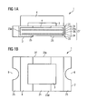
- FIG. 1 shows a modification of an optoelectronic semiconductor device 1.
- Figure 1A represents a sectional view along the dash-dot line in FIG. 1B represents.
- a main body 27 of a connection carrier 2 is formed with two layers of a fiber reinforcement 24.
- the fiber reinforcement 24 is made of glass fibers. In each position of the fiber reinforcement 24, the fibers are each aligned in a direction parallel to a carrier top 21. With respect to an axis perpendicular to the carrier top 21, the fibers of both layers of the fiber reinforcement 24 are rotated by 90 ° from each other.
- the fiber reinforcement 24 is embedded in a silicone matrix 26, wherein the matrix material completely surrounds the fiber reinforcement 24 on all sides.
- carrier underside 22 Opposite the carrier top side 21 of the connection carrier 2 there is a carrier underside 22. Carrier top side 21 and carrier underside 22 are connected to each other via carrier flanks 23a-d.
- the main body 27 has two recesses 8, which extend from the carrier top 21 to the carrier base 22 and interrupt the carrier flanks 23. About the recesses 8, an assembly of the semiconductor device 1 to a not shown, external not belonging to the semiconductor device 1 carrier can be facilitated.
- connection points 25a, 25b are applied, which are designed as a metallization.
- the base body 27 has a roughening or is an adhesion promoter added.
- the metallization is formed by a 30 micron thick copper layer, which is in direct contact with the main body 27.
- a silver layer is applied with a thickness of 2 microns.
- a nickel-gold layer may also be applied to the copper layer, the thickness of the gold preferably being less than 500 nm.
- connection points 25 has a region on the carrier top 21, which is designed for contacting a semiconductor chip 3.
- each of the connection points 25a, 25b which are electrically insulated from one another, has a structuring which is suitable for connecting the semiconductor component to an external carrier, not shown, by soldering or gluing, for example.
- connection points 25a, 25b on the carrier upper side 21 and carrier lower side 22 are electrically connected to one another via a metallization attached to the opposite, penetrated by the recesses 8 carrier flanks 23a, 23b, wherein the additionally formed by the recess 8 surfaces of the base body 27 also covered by the metallization.
- the carrier flanks 23c, 23d are free of metallization and thus electrically insulating.
- a semiconductor chip 3 is attached via, for example, soldering so that it is in direct contact with the areas of the connection points 25, which are located on the carrier top 21.
- a potting 4 for example, made of a silicone.
- the cubic potting body 4 is in direct contact with the semiconductor chip 3 as well as with the connection carrier 2 and, in the context of the manufacturing tolerances, is flush with the carrier flanks 23c, 23d from. Connection carrier 2 and potting 4 completely close the semiconductor chip 3.
- the floor plan of the connection carrier 2 is rectangular, square or hexagonal.
- the thickness of the connection carrier 2 is preferably designed to be as small as possible, wherein the connection carrier 2 has a sufficient mechanical stability, for example, to prevent bending of the connection carrier 2.
- the thickness of the connection carrier 2 is ⁇ 1 mm, preferably ⁇ 0.6 mm, particularly preferably ⁇ 0.4 mm.
- the thickness of the semiconductor chip 3 are not strictly limited, but the thickness is preferably ⁇ 200 .mu.m, more preferably ⁇ 60 .mu.m, in particular ⁇ 25 .mu.m.
- the semiconductor chip 3 may be formed as a thin-film chip, as in the document WO 2005/081319 A1 described.
- the semiconductor chip 3 emits light in the near ultraviolet or in the blue spectral range.
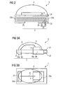
- connection carrier 2 has a three-layer fiber reinforcement 24, each of which, analogous to the exemplary embodiment according to FIG. 1 are twisted 90 ° to each other.
- the main body 27 of the connection carrier 2 has no recesses 8.
- the respective parts of the connection points 25 located on the upper side 21 of the carrier and on the underside of the carrier 22 are connected to one another via the carrier flanks 23a, 23b.
- connection carrier 2 has two plated-through holes 28.
- the Through holes 28 are filled with an electrically and thermally conductive material and form the connection points 25a, 25b.
- the connection point 25a here is made larger than the connection point 25b. Both connection points 25a, 25b project beyond the main body 27 in the direction of the carrier underside 22. This facilitates the attachment of the semiconductor component 1 on a non-subscribed external carrier.
- connection point 25 a On the carrier top 21 of the semiconductor chip 3 is applied directly to the connection point 25 a. This ensures a good thermal contact from the semiconductor chip 3 via the connection point 25a to a not shown, external carrier.
- the second electrical contact of the semiconductor chip 3 is located on a side facing away from the connection carrier 2 of the chip. The electrical contacting takes place via a bonding wire 6 to the connection point 25b.
- Both connection points 25a, 25b and the semiconductor chip 3 and the bonding wire 6 are covered by a lens-like potting body 4 made of a silicone.
- the potting body 4 is in direct contact with the semiconductor chip 3 and the connection carrier 2 and has a spherical-ellipsoidal shape.
- the potting body 4 which may also be designed as a cylindrical lens, at least one admixture 7 in the form of a filter agent, a reflection agent, a diffusion agent or a conversion agent added.
- the admixture 7 may be evenly distributed in the potting 4 or occur locally heaped.
- the concentration of an admixture 7 in regions above the side of the semiconductor chip 3 facing away from the connection carrier 2 may be higher in order to achieve a uniform conversion of electromagnetic radiation emitted by the semiconductor chip 3, for example To ensure radiation in a radiation of a different wavelength.
- a semiconductor chip 3 embodied as a flip chip can also be used as shown in FIG FIG. 1 or FIG. 2 Find use.
- FIG. 4 a further modification of an optoelectronic semiconductor device 1 is shown.
- the electrical contact with a non-subscribed external support via two plated-through holes 28, by means of which two equal-sized connection points 25 are formed by the vias 28 are filled with an electrically conductive material.
- a glass body 5 is attached, which is designed to be transparent to the radiation to be received or emitted by the semiconductor chip 3.
- the gas may be, for example, air, argon or nitrogen.
- the glass body 5 is configured as a lenticular element and laterally terminates flush with the carrier flanks 23, within the framework of the manufacturing tolerances.
- the gap 10 may be filled with a potting body 4.
- the potting body 4 preferably has a liquid or viscous consistency, so that the gap 10 is filled completely and in a form-fitting manner by pressing the glass body 5 in the direction of the connection carrier 2.
- the glass body 5 can in this case have an opening, for example in the lateral direction, so that air bubbles and / or excess, the potting body 4 forming mass of the Gap 10 can escape.
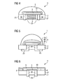
- connection carrier 2 may have a heat sink 9.
- the heat sink 9 extends from the carrier top 21 to the carrier bottom 22.
- the heat sink 9 can be flush with the carrier base 22, as in FIG. 4 shown, or also project beyond the carrier base 22 in correspondence with the connection points 25.
- the heat sink 9 preferably has a high thermal conductivity and also a high heat capacity and is formed, for example, with copper. If the heat sink 9 is electrically conductive, electrical, undesired contacting, for example, via an insulating layer between the semiconductor chip 3 or an external carrier and heat sink 9, not shown, can be avoided.
- connection carrier 2 has two plated-through holes 28, which are filled with a metal or a metal alloy and form the connection points 25.
- the parts of the connection points 25 which are located on the carrier underside 22 are made larger than the cross-sectional areas of the plated-through holes 28. In this way, an improved thermal contact with an external carrier, not shown, is achieved.
- the potting body 4 has a plurality of layers 4a, 4b, 4c.
- An innermost layer 4a may, for example, be designed in a uniform thickness, so that the layer 4a surrounds the semiconductor chip 3 on all sides in a uniform thickness, with the exception of the side facing the connection carrier 2.
- a uniform conversion for example the radiation emitted by the semiconductor chip 3 can be achieved.
- Over the layers 4b, 4c a lens effect can be realized.
- the lens effect can be enhanced if the refractive index of the layer 4b is lower than that of the layer 4c.
- the refractive index of the layer 4c is smaller than that of the layer 4b, which in turn is smaller than that of the layer 4a, which in turn is smaller than that of the semiconductor chip 3. In this way, the Lichtauskoppeleffizienz from the semiconductor chip 3 is increased become.
- the outermost layer 4c of the potting body 4 is designed with a hard silicone, so that an external influences compared to robust semiconductor device 10 results.
- connection points 25 and connection carrier 2 the exemplary embodiment of the semiconductor component 1 corresponds to FIG FIG. 6 the in FIG. 4 shown.
- annular potting body 4 is mounted, which is in direct contact with the carrier top 21, but has no direct contact with the semiconductor chip 3.
- the potting body 4 is designed with a soft silicone.
- a glass body 5 is applied in the form of a glass plate, so that the gap 10 is formed.
- glass body 5 and / or potting 4, as in the modifications according to the FIGS. 1 to 5 , different or even admixtures include.
- the connection points 25 or also the carrier chip side 21 facing the semiconductor chip 3 can be made reflective for the radiation to be emitted or received by the semiconductor chip 3.
- the connection carrier 2 and the potting body 4 as well as the glass body 5 may be transparent or translucent. If the connection points 25 occupy only a small area, then a semiconductor component 1 which is generally substantially at least partially translucent may result.
- a plurality of semiconductor chips emitting, for example, in different spectral regions can be mounted on a single connection carrier 2.
Landscapes
- Engineering & Computer Science (AREA)
- Microelectronics & Electronic Packaging (AREA)
- Led Device Packages (AREA)
- Optical Couplings Of Light Guides (AREA)
Applications Claiming Priority (2)
| Application Number | Priority Date | Filing Date | Title |
|---|---|---|---|
| DE102008025491A DE102008025491A1 (de) | 2008-05-28 | 2008-05-28 | Optoelektronisches Halbleiterbauteil und Leiterplatte |
| PCT/DE2009/000543 WO2009143796A2 (de) | 2008-05-28 | 2009-04-20 | Optoelektronisches halbleiterbauteil und leiterplatte |
Publications (2)
| Publication Number | Publication Date |
|---|---|
| EP2281316A2 EP2281316A2 (de) | 2011-02-09 |
| EP2281316B1 true EP2281316B1 (de) | 2015-06-10 |
Family
ID=41064795
Family Applications (1)
| Application Number | Title | Priority Date | Filing Date |
|---|---|---|---|
| EP09753512.4A Active EP2281316B1 (de) | 2008-05-28 | 2009-04-20 | Optoelektronisches halbleiterbauteil |
Country Status (7)
| Country | Link |
|---|---|
| US (1) | US9397271B2 (enExample) |
| EP (1) | EP2281316B1 (enExample) |
| JP (1) | JP5750040B2 (enExample) |
| KR (1) | KR101541565B1 (enExample) |
| CN (1) | CN101971375B (enExample) |
| DE (1) | DE102008025491A1 (enExample) |
| WO (1) | WO2009143796A2 (enExample) |
Families Citing this family (18)
| Publication number | Priority date | Publication date | Assignee | Title |
|---|---|---|---|---|
| DE102010044470B4 (de) | 2010-09-06 | 2018-06-28 | Heraeus Noblelight Gmbh | Verfahren zur Beschichtung eines optoelektronischen Chip-On-Board-Moduls, optoelektronisches Chip-On-Board-Modul und System damit |
| DE102010054068A1 (de) * | 2010-12-10 | 2012-06-14 | Osram Opto Semiconductors Gmbh | Verfahren zur Herstellung eines optoelektronischen Bauelements und Bauelement |
| JP5795251B2 (ja) | 2011-12-14 | 2015-10-14 | 信越化学工業株式会社 | 光学半導体装置用基台及びその製造方法、並びに光学半導体装置 |
| JP5851875B2 (ja) * | 2012-02-14 | 2016-02-03 | 信越化学工業株式会社 | 光学半導体装置用パッケージの製造方法及び光学半導体装置の製造方法 |
| TWI590494B (zh) | 2012-02-14 | 2017-07-01 | 信越化學工業股份有限公司 | Optical semiconductor device package, its manufacturing method, and optical semiconductor device and its manufacturing method |
| JP5770674B2 (ja) * | 2012-04-04 | 2015-08-26 | 信越化学工業株式会社 | 光学半導体装置用基板及びその製造方法、並びに光学半導体装置 |
| JP5767160B2 (ja) * | 2012-05-07 | 2015-08-19 | 信越化学工業株式会社 | 光学半導体装置用基板の製造方法 |
| DE102012105176B4 (de) * | 2012-06-14 | 2021-08-12 | OSRAM Opto Semiconductors Gesellschaft mit beschränkter Haftung | Optoelektronischer Halbleiterchip |
| JP2014203942A (ja) * | 2013-04-04 | 2014-10-27 | 信越化学工業株式会社 | 光半導体装置 |
| KR102086098B1 (ko) * | 2013-07-03 | 2020-03-09 | 삼성디스플레이 주식회사 | 표시 장치 |
| JP2015165546A (ja) * | 2014-02-07 | 2015-09-17 | 株式会社ミマキエンジニアリング | 紫外線発光ダイオードユニット、紫外線発光ダイオードユニットのセット、インクジェット装置および三次元造形物製造装置 |
| JP6628473B2 (ja) * | 2014-12-26 | 2020-01-08 | 日亜化学工業株式会社 | 発光装置 |
| DE102015115722A1 (de) * | 2015-09-17 | 2017-03-23 | Osram Opto Semiconductors Gmbh | Träger für ein Bauelement, Bauelement und Verfahren zur Herstellung eines Trägers oder eines Bauelements |
| JP6365592B2 (ja) * | 2016-05-31 | 2018-08-01 | 日亜化学工業株式会社 | 発光装置 |
| US10083885B1 (en) * | 2017-06-06 | 2018-09-25 | Cree, Inc. | Multi-layer potting for electronic modules |
| JP7089167B2 (ja) * | 2018-04-23 | 2022-06-22 | 日亜化学工業株式会社 | 発光装置 |
| CN113258274B (zh) * | 2020-02-10 | 2025-06-06 | 东友精细化工有限公司 | 天线堆叠结构和包括天线堆叠结构的显示装置 |
| DE102020111728B4 (de) | 2020-04-29 | 2022-06-23 | Schott Ag | Elektro-optisches Wandlerbauteil mit einem Abstandhalter, sowie Abstandhalter-Wafer zur Herstellung eines elektro-optischen Wandlerbauteils |
Family Cites Families (31)
| Publication number | Priority date | Publication date | Assignee | Title |
|---|---|---|---|---|
| US3568012A (en) * | 1968-11-05 | 1971-03-02 | Westinghouse Electric Corp | A microminiature circuit device employing a low thermal expansion binder |
| GB1583544A (en) * | 1977-07-25 | 1981-01-28 | Uop Inc | Metal-clad laminates |
| JP3417079B2 (ja) * | 1994-08-31 | 2003-06-16 | ソニー株式会社 | 半導体装置の製造方法 |
| DE19942470B4 (de) * | 1998-09-08 | 2013-04-11 | Fujitsu Ltd. | Optisches Halbeitermodul und Verfahren zum Herstellen eines optischen Halbleitermoduls |
| JP2000150701A (ja) * | 1998-11-05 | 2000-05-30 | Shinko Electric Ind Co Ltd | 半導体装置並びにこれに用いる接続用基板及びその製造方法 |
| WO2001059851A1 (fr) | 2000-02-09 | 2001-08-16 | Nippon Leiz Corporation | Source lumineuse |
| JP2001257410A (ja) | 2000-03-09 | 2001-09-21 | Kyocera Corp | 電子部品 |
| US20030141563A1 (en) * | 2002-01-28 | 2003-07-31 | Bily Wang | Light emitting diode package with fluorescent cover |
| US20040038442A1 (en) * | 2002-08-26 | 2004-02-26 | Kinsman Larry D. | Optically interactive device packages and methods of assembly |
| JP4071639B2 (ja) | 2003-01-15 | 2008-04-02 | 信越化学工業株式会社 | 発光ダイオード素子用シリコーン樹脂組成物 |
| US7037592B2 (en) * | 2003-02-25 | 2006-05-02 | Dow Coming Corporation | Hybrid composite of silicone and organic resins |
| EP1604385B1 (de) | 2003-03-10 | 2019-12-11 | OSRAM Opto Semiconductors GmbH | Optoelektronisches bauelement mit einem gehäusekörper aus kunststoffmaterial |
| JP4766222B2 (ja) * | 2003-03-12 | 2011-09-07 | 信越化学工業株式会社 | 発光半導体被覆保護材及び発光半導体装置 |
| JP2005064047A (ja) * | 2003-08-13 | 2005-03-10 | Citizen Electronics Co Ltd | 発光ダイオード |
| US7087465B2 (en) * | 2003-12-15 | 2006-08-08 | Philips Lumileds Lighting Company, Llc | Method of packaging a semiconductor light emitting device |
| CN1914961A (zh) * | 2004-01-20 | 2007-02-14 | 环球产权公司 | 电路材料、电路、多层电路及其制造方法 |
| JP5305594B2 (ja) | 2004-02-20 | 2013-10-02 | オスラム オプト セミコンダクターズ ゲゼルシャフト ミット ベシュレンクテル ハフツング | 光電素子、多数の光電素子を有する装置および光電素子を製造する方法 |
| JP4598432B2 (ja) * | 2004-05-12 | 2010-12-15 | 浜松ホトニクス株式会社 | 電子部品及びその製造方法 |
| US7344902B2 (en) * | 2004-11-15 | 2008-03-18 | Philips Lumileds Lighting Company, Llc | Overmolded lens over LED die |
| US20080296589A1 (en) * | 2005-03-24 | 2008-12-04 | Ingo Speier | Solid-State Lighting Device Package |
| US7288798B2 (en) * | 2005-06-02 | 2007-10-30 | Lighthouse Technology Co., Ltd | Light module |
| DE102006000476A1 (de) * | 2005-09-22 | 2007-05-24 | Lexedis Lighting Gesmbh | Lichtemissionsvorrichtung |
| JP2007180203A (ja) * | 2005-12-27 | 2007-07-12 | Shinko Electric Ind Co Ltd | 半導体装置および半導体装置の製造方法 |
| US7521728B2 (en) * | 2006-01-20 | 2009-04-21 | Cree, Inc. | Packages for semiconductor light emitting devices utilizing dispensed reflectors and methods of forming the same |
| JP4996101B2 (ja) * | 2006-02-02 | 2012-08-08 | 新光電気工業株式会社 | 半導体装置及び半導体装置の製造方法 |
| JP5268082B2 (ja) | 2006-02-22 | 2013-08-21 | シチズン電子株式会社 | 光半導体装置 |
| JP4969119B2 (ja) | 2006-03-20 | 2012-07-04 | 日本碍子株式会社 | 発光ダイオード装置 |
| TW200805694A (en) * | 2006-07-04 | 2008-01-16 | Secure Tech Co Ltd | Light-emitting component and manufacturing method thereof |
| US8735920B2 (en) * | 2006-07-31 | 2014-05-27 | Cree, Inc. | Light emitting diode package with optical element |
| JP4979299B2 (ja) * | 2006-08-03 | 2012-07-18 | 豊田合成株式会社 | 光学装置及びその製造方法 |
| JP2008071955A (ja) * | 2006-09-14 | 2008-03-27 | Nichia Chem Ind Ltd | 発光装置 |
-
2008
- 2008-05-28 DE DE102008025491A patent/DE102008025491A1/de not_active Withdrawn
-
2009
- 2009-04-20 JP JP2011510816A patent/JP5750040B2/ja active Active
- 2009-04-20 KR KR1020107020194A patent/KR101541565B1/ko active Active
- 2009-04-20 US US12/922,240 patent/US9397271B2/en active Active
- 2009-04-20 WO PCT/DE2009/000543 patent/WO2009143796A2/de not_active Ceased
- 2009-04-20 CN CN2009801090657A patent/CN101971375B/zh active Active
- 2009-04-20 EP EP09753512.4A patent/EP2281316B1/de active Active
Also Published As
| Publication number | Publication date |
|---|---|
| KR101541565B1 (ko) | 2015-08-04 |
| CN101971375A (zh) | 2011-02-09 |
| WO2009143796A2 (de) | 2009-12-03 |
| CN101971375B (zh) | 2013-02-20 |
| EP2281316A2 (de) | 2011-02-09 |
| US9397271B2 (en) | 2016-07-19 |
| KR20110016857A (ko) | 2011-02-18 |
| JP5750040B2 (ja) | 2015-07-15 |
| DE102008025491A1 (de) | 2009-12-03 |
| JP2011521481A (ja) | 2011-07-21 |
| WO2009143796A3 (de) | 2010-03-11 |
| US20110108870A1 (en) | 2011-05-12 |
Similar Documents
| Publication | Publication Date | Title |
|---|---|---|
| EP2281316B1 (de) | Optoelektronisches halbleiterbauteil | |
| DE102008025756B4 (de) | Halbleiteranordnung | |
| EP1352432B9 (de) | Lumineszenzdiode und verfahren zu deren herstellung | |
| EP2258000B1 (de) | Optoelektronisches halbleiterbauteil und verfahren zur herstellung eines optoelektronischen halbleiterbauteils | |
| EP1920470B1 (de) | Verfahren zur herstellung eines oberflächenmontierbaren optoelektronischen halbleiterbauelements | |
| EP2483937B1 (de) | Optoelektronisches bauelement | |
| EP2583319B1 (de) | Optoelektronisches bauteil | |
| DE102008021402B4 (de) | Oberflächenmontierbares Leuchtdioden-Modul und Verfahren zur Herstellung eines oberflächenmontierbaren Leuchtdioden-Moduls | |
| DE112019001502B4 (de) | Optoelektronisches bauelement und verfahren zur herstellung eines optoelektronischen bauelements | |
| EP1761959B1 (de) | Leuchtdiodenanordnung | |
| DE102008038748B4 (de) | Oberflächenmontierbares, optoelektronisches Halbleiterbauteil | |
| DE102005045587A1 (de) | Baugruppe mit einem Licht emittierenden Halbleiterelement | |
| DE10033502A1 (de) | Optoelektronisches Modul, Verfahren zu dessen Herstellung und dessen Verwendung | |
| DE102004021233A1 (de) | Leuchtdiodenanordnung | |
| EP2047525A2 (de) | Dünnfilm-halbleiterbauelement und bauelement-verbund | |
| WO2011104364A1 (de) | Strahlungsemittierendes bauelement mit einem halbleiterchip und einem konversionselement und verfahren zu dessen herstellung | |
| WO2014207037A1 (de) | Optoelektronisches bauelement und verfahren zu seiner herstellung | |
| DE102014116529A1 (de) | Optoelektronisches Halbleiterbauteil und Verfahren zur Herstellung eines optoelektronischen Halbleiterbauteils | |
| DE102017102619A1 (de) | Led-einheit | |
| DE102011056220A1 (de) | Optoelektronisches Halbleiterbauteil und Verfahren zur Herstellung eines optoelektronischen Halbleiterbauteils | |
| WO2014048699A1 (de) | Optoelektronisches halbleiterbauteil und verfahren zur herstellung eines optoelektronischen halbleiterbauteils | |
| WO2009103285A1 (de) | Optoelektronisches bauteil | |
| DE102021113592A1 (de) | Optoelektronisches halbleiterbauteil und paneel | |
| WO2012013435A1 (de) | Licht emittierendes halbleiterbauelement und verfahren zur herstellung eines licht emittierenden halbleiterbauelements | |
| DE102020114368A1 (de) | Optoelektronisches halbleiterbauteil und verfahren zur herstellung von optoelektronischen halbleiterbauteilen |
Legal Events
| Date | Code | Title | Description |
|---|---|---|---|
| PUAI | Public reference made under article 153(3) epc to a published international application that has entered the european phase |
Free format text: ORIGINAL CODE: 0009012 |
|
| 17P | Request for examination filed |
Effective date: 20100813 |
|
| AK | Designated contracting states |
Kind code of ref document: A2 Designated state(s): AT BE BG CH CY CZ DE DK EE ES FI FR GB GR HR HU IE IS IT LI LT LU LV MC MK MT NL NO PL PT RO SE SI SK TR |
|
| AX | Request for extension of the european patent |
Extension state: AL BA RS |
|
| DAX | Request for extension of the european patent (deleted) | ||
| RIN1 | Information on inventor provided before grant (corrected) |
Inventor name: TSUTOMU, KASHIWAGI Inventor name: JAEGER, HARALD Inventor name: SORG, JOERG, ERICH Inventor name: TOSHIO, SHIOBARA |
|
| RAP1 | Party data changed (applicant data changed or rights of an application transferred) |
Owner name: SHIN-ETSU CHEMICAL CO., LTD. Owner name: OSRAM OPTO SEMICONDUCTORS GMBH |
|
| 17Q | First examination report despatched |
Effective date: 20141008 |
|
| REG | Reference to a national code |
Ref country code: DE Ref legal event code: R079 Ref document number: 502009011137 Country of ref document: DE Free format text: PREVIOUS MAIN CLASS: H01L0033000000 Ipc: H01L0033480000 |
|
| GRAP | Despatch of communication of intention to grant a patent |
Free format text: ORIGINAL CODE: EPIDOSNIGR1 |
|
| RIC1 | Information provided on ipc code assigned before grant |
Ipc: H01L 33/48 20100101AFI20141216BHEP Ipc: H05K 1/03 20060101ALI20141216BHEP |
|
| INTG | Intention to grant announced |
Effective date: 20150116 |
|
| GRAS | Grant fee paid |
Free format text: ORIGINAL CODE: EPIDOSNIGR3 |
|
| GRAA | (expected) grant |
Free format text: ORIGINAL CODE: 0009210 |
|
| RIN1 | Information on inventor provided before grant (corrected) |
Inventor name: SORG, JOERG, ERICH Inventor name: SHIOBARA, TOSHIO Inventor name: KASHIWAGI, TSUTOMU Inventor name: JAEGER, HARALD |
|
| AK | Designated contracting states |
Kind code of ref document: B1 Designated state(s): AT BE BG CH CY CZ DE DK EE ES FI FR GB GR HR HU IE IS IT LI LT LU LV MC MK MT NL NO PL PT RO SE SI SK TR |
|
| REG | Reference to a national code |
Ref country code: GB Ref legal event code: FG4D Free format text: NOT ENGLISH |
|
| REG | Reference to a national code |
Ref country code: CH Ref legal event code: EP |
|
| REG | Reference to a national code |
Ref country code: AT Ref legal event code: REF Ref document number: 731213 Country of ref document: AT Kind code of ref document: T Effective date: 20150715 |
|
| REG | Reference to a national code |
Ref country code: DE Ref legal event code: R096 Ref document number: 502009011137 Country of ref document: DE |
|
| REG | Reference to a national code |
Ref country code: IE Ref legal event code: FG4D Free format text: LANGUAGE OF EP DOCUMENT: GERMAN |
|
| PG25 | Lapsed in a contracting state [announced via postgrant information from national office to epo] |
Ref country code: NO Free format text: LAPSE BECAUSE OF FAILURE TO SUBMIT A TRANSLATION OF THE DESCRIPTION OR TO PAY THE FEE WITHIN THE PRESCRIBED TIME-LIMIT Effective date: 20150910 Ref country code: ES Free format text: LAPSE BECAUSE OF FAILURE TO SUBMIT A TRANSLATION OF THE DESCRIPTION OR TO PAY THE FEE WITHIN THE PRESCRIBED TIME-LIMIT Effective date: 20150610 Ref country code: LT Free format text: LAPSE BECAUSE OF FAILURE TO SUBMIT A TRANSLATION OF THE DESCRIPTION OR TO PAY THE FEE WITHIN THE PRESCRIBED TIME-LIMIT Effective date: 20150610 Ref country code: FI Free format text: LAPSE BECAUSE OF FAILURE TO SUBMIT A TRANSLATION OF THE DESCRIPTION OR TO PAY THE FEE WITHIN THE PRESCRIBED TIME-LIMIT Effective date: 20150610 |
|
| REG | Reference to a national code |
Ref country code: NL Ref legal event code: MP Effective date: 20150610 |
|
| PG25 | Lapsed in a contracting state [announced via postgrant information from national office to epo] |
Ref country code: LV Free format text: LAPSE BECAUSE OF FAILURE TO SUBMIT A TRANSLATION OF THE DESCRIPTION OR TO PAY THE FEE WITHIN THE PRESCRIBED TIME-LIMIT Effective date: 20150610 Ref country code: GR Free format text: LAPSE BECAUSE OF FAILURE TO SUBMIT A TRANSLATION OF THE DESCRIPTION OR TO PAY THE FEE WITHIN THE PRESCRIBED TIME-LIMIT Effective date: 20150911 Ref country code: BG Free format text: LAPSE BECAUSE OF FAILURE TO SUBMIT A TRANSLATION OF THE DESCRIPTION OR TO PAY THE FEE WITHIN THE PRESCRIBED TIME-LIMIT Effective date: 20150910 |
|
| PG25 | Lapsed in a contracting state [announced via postgrant information from national office to epo] |
Ref country code: EE Free format text: LAPSE BECAUSE OF FAILURE TO SUBMIT A TRANSLATION OF THE DESCRIPTION OR TO PAY THE FEE WITHIN THE PRESCRIBED TIME-LIMIT Effective date: 20150610 |
|
| PG25 | Lapsed in a contracting state [announced via postgrant information from national office to epo] |
Ref country code: PL Free format text: LAPSE BECAUSE OF FAILURE TO SUBMIT A TRANSLATION OF THE DESCRIPTION OR TO PAY THE FEE WITHIN THE PRESCRIBED TIME-LIMIT Effective date: 20150610 Ref country code: CZ Free format text: LAPSE BECAUSE OF FAILURE TO SUBMIT A TRANSLATION OF THE DESCRIPTION OR TO PAY THE FEE WITHIN THE PRESCRIBED TIME-LIMIT Effective date: 20150610 Ref country code: PT Free format text: LAPSE BECAUSE OF FAILURE TO SUBMIT A TRANSLATION OF THE DESCRIPTION OR TO PAY THE FEE WITHIN THE PRESCRIBED TIME-LIMIT Effective date: 20151012 Ref country code: RO Free format text: LAPSE BECAUSE OF NON-PAYMENT OF DUE FEES Effective date: 20150610 Ref country code: IS Free format text: LAPSE BECAUSE OF FAILURE TO SUBMIT A TRANSLATION OF THE DESCRIPTION OR TO PAY THE FEE WITHIN THE PRESCRIBED TIME-LIMIT Effective date: 20151010 Ref country code: SK Free format text: LAPSE BECAUSE OF FAILURE TO SUBMIT A TRANSLATION OF THE DESCRIPTION OR TO PAY THE FEE WITHIN THE PRESCRIBED TIME-LIMIT Effective date: 20150610 |
|
| REG | Reference to a national code |
Ref country code: DE Ref legal event code: R097 Ref document number: 502009011137 Country of ref document: DE |
|
| PLBE | No opposition filed within time limit |
Free format text: ORIGINAL CODE: 0009261 |
|
| STAA | Information on the status of an ep patent application or granted ep patent |
Free format text: STATUS: NO OPPOSITION FILED WITHIN TIME LIMIT |
|
| PG25 | Lapsed in a contracting state [announced via postgrant information from national office to epo] |
Ref country code: DK Free format text: LAPSE BECAUSE OF FAILURE TO SUBMIT A TRANSLATION OF THE DESCRIPTION OR TO PAY THE FEE WITHIN THE PRESCRIBED TIME-LIMIT Effective date: 20150610 Ref country code: IT Free format text: LAPSE BECAUSE OF FAILURE TO SUBMIT A TRANSLATION OF THE DESCRIPTION OR TO PAY THE FEE WITHIN THE PRESCRIBED TIME-LIMIT Effective date: 20150610 |
|
| 26N | No opposition filed |
Effective date: 20160311 |
|
| PG25 | Lapsed in a contracting state [announced via postgrant information from national office to epo] |
Ref country code: SI Free format text: LAPSE BECAUSE OF FAILURE TO SUBMIT A TRANSLATION OF THE DESCRIPTION OR TO PAY THE FEE WITHIN THE PRESCRIBED TIME-LIMIT Effective date: 20150610 |
|
| PG25 | Lapsed in a contracting state [announced via postgrant information from national office to epo] |
Ref country code: BE Free format text: LAPSE BECAUSE OF NON-PAYMENT OF DUE FEES Effective date: 20160430 |
|
| REG | Reference to a national code |
Ref country code: CH Ref legal event code: PL |
|
| GBPC | Gb: european patent ceased through non-payment of renewal fee |
Effective date: 20160420 |
|
| PG25 | Lapsed in a contracting state [announced via postgrant information from national office to epo] |
Ref country code: LU Free format text: LAPSE BECAUSE OF FAILURE TO SUBMIT A TRANSLATION OF THE DESCRIPTION OR TO PAY THE FEE WITHIN THE PRESCRIBED TIME-LIMIT Effective date: 20160420 |
|
| REG | Reference to a national code |
Ref country code: IE Ref legal event code: MM4A |
|
| REG | Reference to a national code |
Ref country code: FR Ref legal event code: ST Effective date: 20161230 |
|
| PG25 | Lapsed in a contracting state [announced via postgrant information from national office to epo] |
Ref country code: FR Free format text: LAPSE BECAUSE OF NON-PAYMENT OF DUE FEES Effective date: 20160502 Ref country code: GB Free format text: LAPSE BECAUSE OF NON-PAYMENT OF DUE FEES Effective date: 20160420 Ref country code: LI Free format text: LAPSE BECAUSE OF NON-PAYMENT OF DUE FEES Effective date: 20160430 Ref country code: CH Free format text: LAPSE BECAUSE OF NON-PAYMENT OF DUE FEES Effective date: 20160430 |
|
| PG25 | Lapsed in a contracting state [announced via postgrant information from national office to epo] |
Ref country code: IE Free format text: LAPSE BECAUSE OF NON-PAYMENT OF DUE FEES Effective date: 20160420 |
|
| REG | Reference to a national code |
Ref country code: AT Ref legal event code: MM01 Ref document number: 731213 Country of ref document: AT Kind code of ref document: T Effective date: 20160420 |
|
| PG25 | Lapsed in a contracting state [announced via postgrant information from national office to epo] |
Ref country code: NL Free format text: LAPSE BECAUSE OF FAILURE TO SUBMIT A TRANSLATION OF THE DESCRIPTION OR TO PAY THE FEE WITHIN THE PRESCRIBED TIME-LIMIT Effective date: 20150610 Ref country code: SE Free format text: LAPSE BECAUSE OF FAILURE TO SUBMIT A TRANSLATION OF THE DESCRIPTION OR TO PAY THE FEE WITHIN THE PRESCRIBED TIME-LIMIT Effective date: 20150610 |
|
| PG25 | Lapsed in a contracting state [announced via postgrant information from national office to epo] |
Ref country code: AT Free format text: LAPSE BECAUSE OF NON-PAYMENT OF DUE FEES Effective date: 20160420 |
|
| PG25 | Lapsed in a contracting state [announced via postgrant information from national office to epo] |
Ref country code: CY Free format text: LAPSE BECAUSE OF FAILURE TO SUBMIT A TRANSLATION OF THE DESCRIPTION OR TO PAY THE FEE WITHIN THE PRESCRIBED TIME-LIMIT Effective date: 20150610 Ref country code: HU Free format text: LAPSE BECAUSE OF FAILURE TO SUBMIT A TRANSLATION OF THE DESCRIPTION OR TO PAY THE FEE WITHIN THE PRESCRIBED TIME-LIMIT; INVALID AB INITIO Effective date: 20090420 |
|
| PG25 | Lapsed in a contracting state [announced via postgrant information from national office to epo] |
Ref country code: HR Free format text: LAPSE BECAUSE OF FAILURE TO SUBMIT A TRANSLATION OF THE DESCRIPTION OR TO PAY THE FEE WITHIN THE PRESCRIBED TIME-LIMIT Effective date: 20150610 Ref country code: MK Free format text: LAPSE BECAUSE OF FAILURE TO SUBMIT A TRANSLATION OF THE DESCRIPTION OR TO PAY THE FEE WITHIN THE PRESCRIBED TIME-LIMIT Effective date: 20150610 Ref country code: TR Free format text: LAPSE BECAUSE OF FAILURE TO SUBMIT A TRANSLATION OF THE DESCRIPTION OR TO PAY THE FEE WITHIN THE PRESCRIBED TIME-LIMIT Effective date: 20150610 Ref country code: MT Free format text: LAPSE BECAUSE OF FAILURE TO SUBMIT A TRANSLATION OF THE DESCRIPTION OR TO PAY THE FEE WITHIN THE PRESCRIBED TIME-LIMIT Effective date: 20150610 Ref country code: MC Free format text: LAPSE BECAUSE OF FAILURE TO SUBMIT A TRANSLATION OF THE DESCRIPTION OR TO PAY THE FEE WITHIN THE PRESCRIBED TIME-LIMIT Effective date: 20150610 |
|
| REG | Reference to a national code |
Ref country code: DE Ref legal event code: R082 Ref document number: 502009011137 Country of ref document: DE Representative=s name: EPPING HERMANN FISCHER PATENTANWALTSGESELLSCHA, DE Ref country code: DE Ref legal event code: R081 Ref document number: 502009011137 Country of ref document: DE Owner name: SHIN-ETSU CHEMICAL CO., LTD., JP Free format text: FORMER OWNERS: OSRAM OPTO SEMICONDUCTORS GMBH, 93055 REGENSBURG, DE; SHIN-ETSU CHEMICAL CO., LTD., TOKYO, JP Ref country code: DE Ref legal event code: R081 Ref document number: 502009011137 Country of ref document: DE Owner name: SHIN-ETSU CHEMICAL CO., LTD., JP Free format text: FORMER OWNERS: OSRAM OPTO SEMICONDUCTORS GESELLSCHAFT MIT BESCHRAENKTER HAFTUNG, 93055 REGENSBURG, DE; SHIN-ETSU CHEMICAL CO., LTD., TOKYO, JP |
|
| REG | Reference to a national code |
Ref country code: DE Ref legal event code: R079 Ref document number: 502009011137 Country of ref document: DE Free format text: PREVIOUS MAIN CLASS: H01L0033480000 Ipc: H10H0020850000 |
|
| PGFP | Annual fee paid to national office [announced via postgrant information from national office to epo] |
Ref country code: DE Payment date: 20250305 Year of fee payment: 17 |