EP2278633A2 - Light emitting device package and method for fabricating the same - Google Patents
Light emitting device package and method for fabricating the same Download PDFInfo
- Publication number
- EP2278633A2 EP2278633A2 EP10169315A EP10169315A EP2278633A2 EP 2278633 A2 EP2278633 A2 EP 2278633A2 EP 10169315 A EP10169315 A EP 10169315A EP 10169315 A EP10169315 A EP 10169315A EP 2278633 A2 EP2278633 A2 EP 2278633A2
- Authority
- EP
- European Patent Office
- Prior art keywords
- light emitting
- substrate
- emitting device
- cavity
- layer
- Prior art date
- Legal status (The legal status is an assumption and is not a legal conclusion. Google has not performed a legal analysis and makes no representation as to the accuracy of the status listed.)
- Granted
Links
Images


Classifications
-
- H—ELECTRICITY
- H10—SEMICONDUCTOR DEVICES; ELECTRIC SOLID-STATE DEVICES NOT OTHERWISE PROVIDED FOR
- H10H—INORGANIC LIGHT-EMITTING SEMICONDUCTOR DEVICES HAVING POTENTIAL BARRIERS
- H10H20/00—Individual inorganic light-emitting semiconductor devices having potential barriers, e.g. light-emitting diodes [LED]
- H10H20/80—Constructional details
- H10H20/81—Bodies
- H10H20/819—Bodies characterised by their shape, e.g. curved or truncated substrates
-
- H—ELECTRICITY
- H10—SEMICONDUCTOR DEVICES; ELECTRIC SOLID-STATE DEVICES NOT OTHERWISE PROVIDED FOR
- H10H—INORGANIC LIGHT-EMITTING SEMICONDUCTOR DEVICES HAVING POTENTIAL BARRIERS
- H10H20/00—Individual inorganic light-emitting semiconductor devices having potential barriers, e.g. light-emitting diodes [LED]
- H10H20/80—Constructional details
- H10H20/83—Electrodes
- H10H20/831—Electrodes characterised by their shape
- H10H20/8312—Electrodes characterised by their shape extending at least partially through the bodies
-
- H—ELECTRICITY
- H10—SEMICONDUCTOR DEVICES; ELECTRIC SOLID-STATE DEVICES NOT OTHERWISE PROVIDED FOR
- H10H—INORGANIC LIGHT-EMITTING SEMICONDUCTOR DEVICES HAVING POTENTIAL BARRIERS
- H10H20/00—Individual inorganic light-emitting semiconductor devices having potential barriers, e.g. light-emitting diodes [LED]
- H10H20/80—Constructional details
- H10H20/83—Electrodes
- H10H20/831—Electrodes characterised by their shape
- H10H20/8314—Electrodes characterised by their shape extending at least partially onto an outer side surface of the bodies
-
- H—ELECTRICITY
- H10—SEMICONDUCTOR DEVICES; ELECTRIC SOLID-STATE DEVICES NOT OTHERWISE PROVIDED FOR
- H10H—INORGANIC LIGHT-EMITTING SEMICONDUCTOR DEVICES HAVING POTENTIAL BARRIERS
- H10H20/00—Individual inorganic light-emitting semiconductor devices having potential barriers, e.g. light-emitting diodes [LED]
- H10H20/80—Constructional details
- H10H20/85—Packages
- H10H20/8506—Containers
-
- H—ELECTRICITY
- H10—SEMICONDUCTOR DEVICES; ELECTRIC SOLID-STATE DEVICES NOT OTHERWISE PROVIDED FOR
- H10H—INORGANIC LIGHT-EMITTING SEMICONDUCTOR DEVICES HAVING POTENTIAL BARRIERS
- H10H20/00—Individual inorganic light-emitting semiconductor devices having potential barriers, e.g. light-emitting diodes [LED]
- H10H20/80—Constructional details
- H10H20/84—Coatings, e.g. passivation layers or antireflective coatings
-
- H—ELECTRICITY
- H10—SEMICONDUCTOR DEVICES; ELECTRIC SOLID-STATE DEVICES NOT OTHERWISE PROVIDED FOR
- H10W—GENERIC PACKAGES, INTERCONNECTIONS, CONNECTORS OR OTHER CONSTRUCTIONAL DETAILS OF DEVICES COVERED BY CLASS H10
- H10W72/00—Interconnections or connectors in packages
- H10W72/071—Connecting or disconnecting
- H10W72/073—Connecting or disconnecting of die-attach connectors
-
- H—ELECTRICITY
- H10—SEMICONDUCTOR DEVICES; ELECTRIC SOLID-STATE DEVICES NOT OTHERWISE PROVIDED FOR
- H10W—GENERIC PACKAGES, INTERCONNECTIONS, CONNECTORS OR OTHER CONSTRUCTIONAL DETAILS OF DEVICES COVERED BY CLASS H10
- H10W72/00—Interconnections or connectors in packages
- H10W72/071—Connecting or disconnecting
- H10W72/075—Connecting or disconnecting of bond wires
-
- H—ELECTRICITY
- H10—SEMICONDUCTOR DEVICES; ELECTRIC SOLID-STATE DEVICES NOT OTHERWISE PROVIDED FOR
- H10W—GENERIC PACKAGES, INTERCONNECTIONS, CONNECTORS OR OTHER CONSTRUCTIONAL DETAILS OF DEVICES COVERED BY CLASS H10
- H10W72/00—Interconnections or connectors in packages
- H10W72/851—Dispositions of multiple connectors or interconnections
- H10W72/874—On different surfaces
- H10W72/884—Die-attach connectors and bond wires
Definitions
- This embodiment relates to a light emitting device and a method for fabricating the same.
- a light emitting device includes a p-n junction diode which converts electric energy into light energy.
- the p-n junction diode is manufactured by combining group 3 elements of the periodic table with group 5 elements of the periodic table.
- the LED can create various colors by adjusting a composition of a compound semiconductor.
- the p-n junction diode When a forward voltage is applied, electrons of an n-layer and holes of a p-layer are coupled to each other, so that the p-n junction diode emits energy equivalent to the energy gap between a conduction band and a valance band.
- the energy is emitted in the form of heat or light. It is the LED that emits the energy in the form of light.
- a nitride semiconductor has high thermal stability and wide band gap energy, more and more attention is paid to the nitride semiconductor in the field of developing an optical device and a high output electronic device.
- a light emitting device such as a blue light emitting device, a green light emitting device and an UV light emitting device and the like which use the nitride semiconductor are commercialized and widely used.
- a light emitting device is manufactured on a substrate.
- a light emitting device chip is separated from the light emitting device through die separation process that is a kind of a sawing process. Then, the light emitting device chip is die-bonded to the package body. Subsequently, a wire bonding process and a molding process are performed, and then a test process is performed.
- the light emitting device package includes: a trench formed in a substrate; a light emitting structure which is directly grown on a first area of the trench in the substrate; an electrode on the substrate; a wire bonding connecting the electrode with the light emitting structure; and a filler filling the trench.
- Another aspect of this invention is a method for fabricating a light emitting device package.
- the method includes: forming a trench in a substrate; forming a light emitting structure on a first area of the trench; forming an electrode on the substrate; performing a wire bonding process between the electrode and the light emitting structure; and filling the trench with a filler.
- each layer (film), an area, a pattern or structures are formed “on/over” or “under” a substrate, each layer (film), an area, a pad or a pattern, it means that the mention includes a case where each layer (film), an area, a pattern or structures are formed “directly” or “by interposing another layer (indirectly)”.
- a criterion for "on/over” and "under” of each layer will be described based on the drawings.
- each layer is magnified, omitted or schematically shown for the purpose of convenience and clearness of description.
- the size of each component does not necessarily mean its actual size.
- Fig. 1 is a cross sectional view of a light emitting device package according to an embodiment.
- Figs. 2 to 9 are cross sectional views showing a method for fabricating a light emitting device package according to an embodiment.
- a light emitting device is referred to as a LED.
- a separate chip process such as Fab process is not required because an LED Epi growth process, a chip process and a packaging process are performed on a substrate.
- the embodiment employs the current injection method applied to a vertical chip. Therefore, it is possible to obtain excellent current spreading effect and high package efficiency.
- a light emitting device is referred to as a LED.
- a trench "C" is formed in a substrate 110.
- a first pattern 310 is formed on the substrate 110, and the substrate 110 is etched by using the first pattern 310 as a mask, so that the trench "C" is formed.
- the substrate 110 is a silicon substrate
- the trench is formed to have a predetermined angle in accordance with the crystal orientation of the silicon substrate.
- the trench is not limited to this shape.
- the first pattern 310 may be formed not only on the substrate 110 but beneath the substrate 110.
- a conductive substrate and a crystalline substrate and the like can be used as the substrate 110.
- the substrate 110 includes a silicon substrate, GaN substrate, GaO substrate, a SiC substrate, a ZnO substrate and a GaAs substrate and the like.
- the substrate 110 is not limited to this kind of substrates.
- a first chip area 100 and a second chip area 200 may be formed.
- the first chip area 100 will be mainly described.
- the first chip area 100 and the second chip area 200 are not sawed from the substrate 100 until both of a chip process and a packaging process are completed.
- the first chip area 100 and the second chip area 200 can be sawed from the substrate 100 after the packaging process is completed.
- Fig. 3 is a view showing an enlarged first chip area 100.
- Fig. 3 does not mean that the first chip area 100 is separated from the substrate 110.
- Fig. 3 merely shows the first chip area 100 conceptually.
- a shape shown in Fig. 3 can be provided.
- the through hole is partially obliquely formed.
- the through hole can have a straight line shape in a vertical direction.
- an insulation layer 120 is formed on the surface of the substrate 110 except a first area "A" in the trench.
- the insulation layer 120 may be formed by forming a second pattern (not shown) on the first area "A” and using SiO 2 film through thermal oxidation and the like.
- the method for forming the insulation layer 120 is not limited to this.
- the insulation layer 120 functions as a mask growing an LED chip at a desired part, for example, an area of the substrate 100 in which the trench is formed.
- the second pattern is removed and a buffer layer 130 is formed on the first area in the trench.
- the buffer layer 130 is formed of silicon carbide (SiC) such that a crystal lattice of the substrate 110 matches with a crystal lattice of the a light emitting structure 140 to be formed later in order to prevent a crystal lattice defect caused by a crystal lattice difference between the substrate 110 and a light emitting structure 140.
- SiC silicon carbide
- the material of the buffer layer 130 is not limited to this.
- the buffer layer 130 may include AlN and ALGaN.
- the buffer layer 130 can be formed by using RF-CVD and the like at a high temperature.
- a method for forming the buffer layer 130 is not limited to this. After photoresist is applied on the insulation layer 120, the first area on which the buffer layer 130 is to be formed may be removed by a masking process and a solvent. Then, the buffer layer 130 is grown on the first area.
- a first reflector metal layer (not shown) may be formed before the buffer layer 130 is formed.
- the first reflector metal layer may include Ti, Pa and the like. Whe the first reflector metal layer include such materials as Ti, Pa, and the like, the first reflector metal layer may not be oxidized during a subsequent process of forming the buffer layer 130.
- a light emitting structure 140 is formed either on the substrate 110 of the first area or on the buffer layer 130. According to the embodiment, a separate pattern is not necessarily required to form the light emitting structure 140 because the Epi layer of the light emitting structure 140 is not grown on the insulation layer 120.
- the embodiment of the present invention includes a method using a homogeneous compound semiconductor, while a conventional technology includes a method using Ag series material or epoxy series material. Therefore, it is possible to obtain high thermal conductivity and high electrical conductivity through the embodiment of the present invention.
- Fig. 7 is a view showing an enlarged light emitting structure 140.
- the light emitting structure is formed of GaN, GaAs, GaAsP, GaP and the like.
- a green LED and a blue LED are formed of GaN of InGaN.
- a yellow LED and a red LED are formed of InGaAIP or AlGaAs. Based on a variety of material composition, full color can be also implemented.
- the light emitting structure 140 includes a second conductive semiconductor layer 142, an active layer 144 and a first conductive semiconductor layer 146.
- the order of forming the light emitting structure 140 is not limited to the stacking order of Fig. 7 .
- a p-type GaN layer is formed as the second conductive semiconductor layer 142 by injecting (EtCp 2 Mg) ⁇ Mg(C 2 H 5 C 5 H 4 ) 2 ⁇ including a p-type impurity such as TMGa gas, NH 3 gas, N 2 gas and Mg into a chamber.
- the second conductive semiconductor layer 142 is not limited to this.
- the active layer 144 emits light having energy determined by a unique energy band of the active layer (i.e., a light emitting layer) when electrons injected through the first conductive semiconductor layer 146 meet the holes injected through the second conductive semiconductor layer 142.
- the active layer 144 may include a quantum well structure formed by stacking once or several times nitride semiconductor thin films having different energy bands.
- the active layer 144 may include a multiple quantum well structure having a InGaN/GaN structure formed by injecting TMGa gas, NH 3 gas, N 2 gas and TMIn gas.
- the quantum well structure is not limited to this.
- An n-type GaN layer may be formed as the first conductive semiconductor layer 146 by using a chemical vapor deposition (CVD), molecular beam epitaxy (MBE), a sputtering method or hydroxide vapor phase epitaxy (HVPE) and the like. Also, the first conductive semiconductor layer 146 may be formed by injecting SiH 4 gas including a n-type impurity such as TMGa gas, NH 3 gas, N 2 gas and Si into a chamber.
- CVD chemical vapor deposition
- MBE molecular beam epitaxy
- HVPE hydroxide vapor phase epitaxy
- an electrode 150 may be formed on the substrate 110.
- the electrode 150 may be formed on some areas of the insulation layer 120.
- the electrode 150 can be insulated from the substrate 110 due to the insulation layer 120 interposed therebetween.
- the upper part of the light emitting device may include a p-type or an n-type electrode having a polarity different from that of the lower of the light emitting device.
- the electrode 150 may be formed of a material having excellent reflexibility and also functions as a reflective layer. Meanwhile, a second reflective layer (not shown) may be formed on the lateral surface of a trench having no electrode 150 formed thereon
- the electrode 150 and the light emitting structure 140 may be coupled by a wire-bonding 160.
- the packaging process is completed by performing a molding process of filling the trench with filler 170.
- the filler 170 includes epoxy resin and silicon resin and the like and is not limited to this.
- a molding process may be performed by using a fluorescent substance (not shown) so as to create a white light.
- a fluorescent substance such as YAG, TAG and the like may be added to a blue LED.
- red, green and blue three fluorescent substances are applied to an UV LED.
- the LED package having LEDs formed therein may be sawed from the substrate based on each chip area and may be manufactured into a product through measurements and tests.
- a separate chip process such as Fab process is not required because an LED Epi growth process, a chip process and a packaging process are performed on a substrate.
- the embodiment of the present invention includes a method using a homogeneous compound semiconductor, while a conventional technology includes a method using Ag series material or epoxy series material. Therefore, it is possible to obtain high thermal conductivity and high electrical conductivity through the embodiment of the present invention.
- the embodiment employs the current injection method applied to a vertical chip. Therefore, it is possible to obtain excellent current spreading effect and high package efficiency.
Landscapes
- Led Device Packages (AREA)
- Led Devices (AREA)
Abstract
a filler filling the trench.
Description
- This embodiment relates to a light emitting device and a method for fabricating the same.
- A light emitting device (LED) includes a p-n junction diode which converts electric energy into light energy. The p-n junction diode is manufactured by combining group 3 elements of the periodic table with group 5 elements of the periodic table. The LED can create various colors by adjusting a composition of a compound semiconductor.
- When a forward voltage is applied, electrons of an n-layer and holes of a p-layer are coupled to each other, so that the p-n junction diode emits energy equivalent to the energy gap between a conduction band and a valance band. The energy is emitted in the form of heat or light. It is the LED that emits the energy in the form of light.
- For example, since a nitride semiconductor has high thermal stability and wide band gap energy, more and more attention is paid to the nitride semiconductor in the field of developing an optical device and a high output electronic device. Particularly, a light emitting device such as a blue light emitting device, a green light emitting device and an UV light emitting device and the like which use the nitride semiconductor are commercialized and widely used.
- Meanwhile, the following process is applied to a light emitting device package according to a conventional technology. A light emitting device is manufactured on a substrate. A light emitting device chip is separated from the light emitting device through die separation process that is a kind of a sawing process. Then, the light emitting device chip is die-bonded to the package body. Subsequently, a wire bonding process and a molding process are performed, and then a test process is performed.
- However, as the conventional technology performs fabricating a light emitting device chip and packaging process separately,various complex processes and many substrates are required.
- One aspect of this invention is a light emitting device package. The light emitting device package includes: a trench formed in a substrate; a light emitting structure which is directly grown on a first area of the trench in the substrate; an electrode on the substrate; a wire bonding connecting the electrode with the light emitting structure; and a filler filling the trench.
- Another aspect of this invention is a method for fabricating a light emitting device package. The method includes: forming a trench in a substrate; forming a light emitting structure on a first area of the trench; forming an electrode on the substrate; performing a wire bonding process between the electrode and the light emitting structure; and filling the trench with a filler.
- The embodiment will be described in detail with reference to the following drawings.
-
Fig. 1 is a cross sectional view of a light emitting device package according to an embodiment. -
Figs. 2 to 9 are cross sectional views showing a method for fabricating a light emitting device package according to an embodiment. - In description of embodiments, when it is mentioned that each layer (film), an area, a pattern or structures are formed "on/over" or "under" a substrate, each layer (film), an area, a pad or a pattern, it means that the mention includes a case where each layer (film), an area, a pattern or structures are formed "directly" or "by interposing another layer (indirectly)". A criterion for "on/over" and "under" of each layer will be described based on the drawings.
- A thickness or size of each layer is magnified, omitted or schematically shown for the purpose of convenience and clearness of description. The size of each component does not necessarily mean its actual size.
-
Fig. 1 is a cross sectional view of a light emitting device package according to an embodiment.Figs. 2 to 9 are cross sectional views showing a method for fabricating a light emitting device package according to an embodiment. Hereinafter, a light emitting device is referred to as a LED. - In accordance with a LED package and a method for fabricating the same according to an embodiment, a separate chip process such as Fab process is not required because an LED Epi growth process, a chip process and a packaging process are performed on a substrate.
- In conventional technology, Ag series material or epoxy series material are used so that an LED chip is die-bonded to the package body, while the embodiment of the present invention uses a homogeneous compound semiconductor. Therefore, it is possible to obtain high thermal conductivity and high electrical conductivity through the embodiment of the present invention.
- In addition, the embodiment employs the current injection method applied to a vertical chip. Therefore, it is possible to obtain excellent current spreading effect and high package efficiency.
- Hereinafter, the method for fabricating a light emitting device package according to an embodiment will be described with reference to
Figs. 2 to 9 . Hereinafter, a light emitting device is referred to as a LED. - First, as shown in
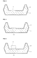
Fig. 2 , a trench "C" is formed in asubstrate 110. For example, afirst pattern 310 is formed on thesubstrate 110, and thesubstrate 110 is etched by using thefirst pattern 310 as a mask, so that the trench "C" is formed. If thesubstrate 110 is a silicon substrate, the trench is formed to have a predetermined angle in accordance with the crystal orientation of the silicon substrate. However, the trench is not limited to this shape. Thefirst pattern 310 may be formed not only on thesubstrate 110 but beneath thesubstrate 110. - A conductive substrate and a crystalline substrate and the like can be used as the
substrate 110. For example, thesubstrate 110 includes a silicon substrate, GaN substrate, GaO substrate, a SiC substrate, a ZnO substrate and a GaAs substrate and the like. Thesubstrate 110 is not limited to this kind of substrates. - Through the etching process, a
first chip area 100 and asecond chip area 200 may be formed. Hereinafter, thefirst chip area 100 will be mainly described. Here, thefirst chip area 100 and thesecond chip area 200 are not sawed from thesubstrate 100 until both of a chip process and a packaging process are completed. Thefirst chip area 100 and thesecond chip area 200 can be sawed from thesubstrate 100 after the packaging process is completed. -
Fig. 3 is a view showing an enlargedfirst chip area 100. Here, as described above, according to the embodiment,Fig. 3 does not mean that thefirst chip area 100 is separated from thesubstrate 110.Fig. 3 merely shows thefirst chip area 100 conceptually. - Of course, when a through hole (not shown) is formed and a cross sectional view is shown on the basis of the through hole, a shape shown in
Fig. 3 can be provided. Here, when a wet etching is performed depending on the crystal orientation of thesubstrate 110, the through hole is partially obliquely formed. However the shape of the through hole is not limited to this. The through hole can have a straight line shape in a vertical direction. - As shown in
Fig. 4 , aninsulation layer 120 is formed on the surface of thesubstrate 110 except a first area "A" in the trench. For example, theinsulation layer 120 may be formed by forming a second pattern (not shown) on the first area "A" and using SiO2 film through thermal oxidation and the like. The method for forming theinsulation layer 120 is not limited to this. - The
insulation layer 120 functions as a mask growing an LED chip at a desired part, for example, an area of thesubstrate 100 in which the trench is formed. - As shown in
Fig. 5 , the second pattern is removed and abuffer layer 130 is formed on the first area in the trench. - The
buffer layer 130 is formed of silicon carbide (SiC) such that a crystal lattice of thesubstrate 110 matches with a crystal lattice of the alight emitting structure 140 to be formed later in order to prevent a crystal lattice defect caused by a crystal lattice difference between thesubstrate 110 and alight emitting structure 140. However, the material of thebuffer layer 130 is not limited to this. For example, thebuffer layer 130 may include AlN and ALGaN. - For example, the
buffer layer 130 can be formed by using RF-CVD and the like at a high temperature. A method for forming thebuffer layer 130 is not limited to this. After photoresist is applied on theinsulation layer 120, the first area on which thebuffer layer 130 is to be formed may be removed by a masking process and a solvent. Then, thebuffer layer 130 is grown on the first area. - Meanwhile, when a SiC substrate is used as the
substrate 110, the crystal lattice of thelight emitting structure 140 may match with the crystal lattice of thesubstrate 110. Therefore, it is possible to produce thelight emitting structure 140 without forming the buffer layer 130.In the embodiment, a first reflector metal layer (not shown) may be formed before thebuffer layer 130 is formed. For example, in the embodiment, the first reflector metal layer may include Ti, Pa and the like. Whe the first reflector metal layer include such materials as Ti, Pa, and the like, the first reflector metal layer may not be oxidized during a subsequent process of forming thebuffer layer 130. - As shown in
Fig. 6 , alight emitting structure 140 is formed either on thesubstrate 110 of the first area or on thebuffer layer 130. According to the embodiment, a separate pattern is not necessarily required to form thelight emitting structure 140 because the Epi layer of thelight emitting structure 140 is not grown on theinsulation layer 120. - In a case where an existing LED chip is die-bonded to the package body, the embodiment of the present invention includes a method using a homogeneous compound semiconductor, while a conventional technology includes a method using Ag series material or epoxy series material. Therefore, it is possible to obtain high thermal conductivity and high electrical conductivity through the embodiment of the present invention.
- Additionally, it is possible to overcome the reliability problem caused by transformation or discoloration due to the thermal resistance of a die adhesive
-
Fig. 7 is a view showing an enlargedlight emitting structure 140. - In the embodiment, the light emitting structure is formed of GaN, GaAs, GaAsP, GaP and the like. For example, a green LED and a blue LED are formed of GaN of InGaN. A yellow LED and a red LED are formed of InGaAIP or AlGaAs. Based on a variety of material composition, full color can be also implemented.
- The
light emitting structure 140 includes a secondconductive semiconductor layer 142, anactive layer 144 and a firstconductive semiconductor layer 146. The order of forming thelight emitting structure 140 is not limited to the stacking order ofFig. 7 . - A p-type GaN layer is formed as the second
conductive semiconductor layer 142 by injecting (EtCp2Mg) {Mg(C2H5C5H4)2} including a p-type impurity such as TMGa gas, NH3 gas, N2 gas and Mg into a chamber. The secondconductive semiconductor layer 142 is not limited to this. - The
active layer 144 emits light having energy determined by a unique energy band of the active layer (i.e., a light emitting layer) when electrons injected through the firstconductive semiconductor layer 146 meet the holes injected through the secondconductive semiconductor layer 142.
Theactive layer 144 may include a quantum well structure formed by stacking once or several times nitride semiconductor thin films having different energy bands. For example, theactive layer 144 may include a multiple quantum well structure having a InGaN/GaN structure formed by injecting TMGa gas, NH3 gas, N2 gas and TMIn gas. The quantum well structure is not limited to this. - An n-type GaN layer may be formed as the first
conductive semiconductor layer 146 by using a chemical vapor deposition (CVD), molecular beam epitaxy (MBE), a sputtering method or hydroxide vapor phase epitaxy (HVPE) and the like. Also, the firstconductive semiconductor layer 146 may be formed by injecting SiH4 gas including a n-type impurity such as TMGa gas, NH3 gas, N2 gas and Si into a chamber. - Next, as shown in
Fig. 8 , anelectrode 150 may be formed on thesubstrate 110. For example, theelectrode 150 may be formed on some areas of theinsulation layer 120. Theelectrode 150 can be insulated from thesubstrate 110 due to theinsulation layer 120 interposed therebetween. - In the embodiment, since the lower part of the
light emitting structure 140 includes the electrically conductive buffer layer or the electrically conductive substrate which are made of an n-type or a p-type electrode, the upper part of the light emitting device may include a p-type or an n-type electrode having a polarity different from that of the lower of the light emitting device. - The
electrode 150 may be formed of a material having excellent reflexibility and also functions as a reflective layer. Meanwhile, a second reflective layer (not shown) may be formed on the lateral surface of a trench having noelectrode 150 formed thereon - Then, the
electrode 150 and thelight emitting structure 140 may be coupled by a wire-bonding 160. - As shown in
Fig. 9 , the packaging process is completed by performing a molding process of filling the trench withfiller 170. For example, thefiller 170 includes epoxy resin and silicon resin and the like and is not limited to this. - In the embodiment, a molding process may be performed by using a fluorescent substance (not shown) so as to create a white light. For example, a yellow fluorescent substance such as YAG, TAG and the like may be added to a blue LED. For another example, red, green and blue three fluorescent substances are applied to an UV LED.
- The LED package having LEDs formed therein may be sawed from the substrate based on each chip area and may be manufactured into a product through measurements and tests.
- In accordance with a LED package and a method for fabricating the same according to an embodiment, a separate chip process such as Fab process is not required because an LED Epi growth process, a chip process and a packaging process are performed on a substrate.
- In a case where an existing LED chip is die-bonded to the package body, the embodiment of the present invention includes a method using a homogeneous compound semiconductor, while a conventional technology includes a method using Ag series material or epoxy series material. Therefore, it is possible to obtain high thermal conductivity and high electrical conductivity through the embodiment of the present invention.
- In addition, the embodiment employs the current injection method applied to a vertical chip. Therefore, it is possible to obtain excellent current spreading effect and high package efficiency.
- The foregoing embodiments and advantages are merely exemplary and are not to be construed as limiting the present invention. The present teaching can be readily applied to other types of apparatuses. The description of the foregoing embodiments is intended to be illustrative, and not to limit the scope of the claims. Many alternatives, modifications, and variations will be apparent to those skilled in the art. In the claims, means-plus-function clauses are intended to cover the structures described herein as performing the recited function and not only structural equivalents but also equivalent structures. Moreover, unless the term "means" is explicitly recited in a limitation of the claims, such limitation is not intended to be interpreted under 35 USC 112(6).
Claims (15)
- A light emitting device package comprising:a cavity formed in a substrate;a light emitting structure directly grown on a portion of the substrate surface that is within cavity;an electrode on the substrate; anda wire bond connecting the electrode with the light emitting structure.
- The light emitting device of claim 1 further comprising:a resin filler in the cavity.
- The light emitting device of claim 2 further comprising:a fluorescent material in the cavity.
- The light emitting device of claim 1, comprising an insulation layer formed on the surface of the substrate excluding the portion of the substrate surface, that is within the cavity, on which the light emitting structure is grown.
- The light emitting device of claim 1, wherein the light emitting structure comprises a buffer layer, and wherein the buffer layer is directly on the portion of the substrate surface, that is within the cavity, on which the light emitting structure is grown.
- The light emitting device of claim 5, wherein the buffer layer comprises a silicon carbide layer.
- The light emitting device of claim 1, wherein the electrode comprises a reflective layer.
- A method for fabricating a light emitting device package, the method comprising:forming a cavity in a substrate;forming a light emitting structure directly on a portion of the substrate surface that is within the cavity;forming an electrode on the substrate; andwire-bonding the light emitting structure to the electrode.
- The method of claim 8 further comprising:placing a resin filler in the cavity.
- The method of claim 9 further comprising:placing a fluorescent material in the cavity.
- The method of claim 8 further comprising:after forming the cavity, forming an insulation layer on the substrate surface excluding that portion of the substrate surface, that is within the cavity, on which the light emitting structure is grown.
- The method of claim 8, wherein forming the light emitting structure directly on a portion of the substrate surface that is within the cavity further comprises:forming a buffer layer directly on that portion of the substrate surface, that is within the cavity, on which the light emitting structure is grown.
- The method of claim 12, wherein the buffer layer comprises a silicon carbide layer.
- The method of claim 8, wherein forming the electrode on the substrate comprises:forming the electrode at least partially on the insulation layer.
- The method of claim 8, wherein the electrode comprises a reflective layer.
Applications Claiming Priority (1)
| Application Number | Priority Date | Filing Date | Title |
|---|---|---|---|
| KR1020090067782A KR101081055B1 (en) | 2009-07-24 | 2009-07-24 | Light emitting device package and method for fabricating the same |
Publications (3)
| Publication Number | Publication Date |
|---|---|
| EP2278633A2 true EP2278633A2 (en) | 2011-01-26 |
| EP2278633A3 EP2278633A3 (en) | 2015-12-02 |
| EP2278633B1 EP2278633B1 (en) | 2019-05-08 |
Family
ID=42937201
Family Applications (1)
| Application Number | Title | Priority Date | Filing Date |
|---|---|---|---|
| EP10169315.8A Not-in-force EP2278633B1 (en) | 2009-07-24 | 2010-07-12 | Light emitting device package and method for fabricating the same |
Country Status (6)
| Country | Link |
|---|---|
| US (1) | US8659046B2 (en) |
| EP (1) | EP2278633B1 (en) |
| JP (1) | JP5739118B2 (en) |
| KR (1) | KR101081055B1 (en) |
| CN (1) | CN101964388B (en) |
| TW (1) | TWI513062B (en) |
Families Citing this family (4)
| Publication number | Priority date | Publication date | Assignee | Title |
|---|---|---|---|---|
| CN102969433A (en) * | 2012-12-06 | 2013-03-13 | 上海顿格电子贸易有限公司 | LED (Light-Emitting Diode) wafer modularized packaging process |
| KR102008315B1 (en) * | 2013-01-23 | 2019-10-21 | 삼성전자주식회사 | Light emitting device package |
| JP6294113B2 (en) * | 2014-03-17 | 2018-03-14 | 新光電気工業株式会社 | Cap and manufacturing method thereof, semiconductor device and manufacturing method thereof |
| CN114038967B (en) * | 2021-07-27 | 2023-05-16 | 重庆康佳光电技术研究院有限公司 | LED epitaxial structure, manufacturing method thereof and LED device |
Family Cites Families (27)
| Publication number | Priority date | Publication date | Assignee | Title |
|---|---|---|---|---|
| JPS5436473B2 (en) * | 1972-01-18 | 1979-11-09 | ||
| JP2898320B2 (en) * | 1989-11-30 | 1999-05-31 | 京セラ株式会社 | Method for manufacturing semiconductor device |
| JPH07106702A (en) * | 1993-10-05 | 1995-04-21 | Hitachi Ltd | Manufacturing method of light emitting and receiving device |
| JPH0983015A (en) * | 1995-09-20 | 1997-03-28 | Oki Electric Ind Co Ltd | Method for manufacturing monolithic light emitting diode array |
| JPH09249499A (en) * | 1996-03-15 | 1997-09-22 | Matsushita Electron Corp | Method for epitaxial growth of group III nitride semiconductor |
| JPH10173236A (en) * | 1996-12-13 | 1998-06-26 | Sharp Corp | Method of manufacturing gallium nitride based compound semiconductor light emitting device |
| JP3785820B2 (en) * | 1998-08-03 | 2006-06-14 | 豊田合成株式会社 | Light emitting device |
| JP4307113B2 (en) * | 2002-03-19 | 2009-08-05 | 宣彦 澤木 | Semiconductor light emitting device and manufacturing method thereof |
| JP4277583B2 (en) * | 2003-05-27 | 2009-06-10 | パナソニック電工株式会社 | Semiconductor light emitting device |
| JP3976723B2 (en) * | 2003-10-30 | 2007-09-19 | 三洋電機株式会社 | Semiconductor device and manufacturing method thereof |
| JP4572312B2 (en) * | 2004-02-23 | 2010-11-04 | スタンレー電気株式会社 | LED and manufacturing method thereof |
| KR20060037638A (en) | 2004-10-28 | 2006-05-03 | 엘지이노텍 주식회사 | Nitride semiconductor light emitting device using silicon substrate and its manufacturing method |
| JP2006237141A (en) * | 2005-02-23 | 2006-09-07 | Stanley Electric Co Ltd | Submount type LED |
| JP2006253288A (en) * | 2005-03-09 | 2006-09-21 | Fuji Photo Film Co Ltd | Light emitting device and manufacturing method thereof |
| KR100746783B1 (en) * | 2006-02-28 | 2007-08-06 | 엘지전자 주식회사 | Light emitting device package and its manufacturing method |
| JP4830768B2 (en) * | 2006-05-10 | 2011-12-07 | 日亜化学工業株式会社 | Semiconductor light emitting device and method for manufacturing semiconductor light emitting device |
| JP5148849B2 (en) * | 2006-07-27 | 2013-02-20 | スタンレー電気株式会社 | LED package, light emitting device using the same, and method of manufacturing LED package |
| TWI418054B (en) * | 2006-08-08 | 2013-12-01 | Lg電子股份有限公司 | Light emitting device package and method of manufacturing the same |
| KR100813070B1 (en) * | 2006-09-29 | 2008-03-14 | 엘지전자 주식회사 | Light emitting device package and its manufacturing method |
| KR100850945B1 (en) | 2006-11-08 | 2008-08-08 | 엘지전자 주식회사 | Light emitting device package and its manufacturing method |
| JP4836769B2 (en) * | 2006-12-18 | 2011-12-14 | スタンレー電気株式会社 | Semiconductor light emitting device and manufacturing method thereof |
| KR100851183B1 (en) * | 2006-12-27 | 2008-08-08 | 엘지이노텍 주식회사 | Semiconductor light emitting device package |
| JP4907476B2 (en) * | 2007-03-13 | 2012-03-28 | コバレントマテリアル株式会社 | Nitride semiconductor single crystal |
| KR100896282B1 (en) * | 2007-11-01 | 2009-05-08 | 엘지전자 주식회사 | Light emitting device package and its manufacturing method |
| KR100891800B1 (en) * | 2007-11-23 | 2009-04-07 | 삼성전기주식회사 | Light emitting device array manufacturing method and light emitting device array |
| JP5258285B2 (en) * | 2007-12-28 | 2013-08-07 | Dowaエレクトロニクス株式会社 | Semiconductor light emitting device |
| KR101114592B1 (en) * | 2009-02-17 | 2012-03-09 | 엘지이노텍 주식회사 | Lighting emitting device and fabrication method thereof |
-
2009
- 2009-07-24 KR KR1020090067782A patent/KR101081055B1/en not_active Expired - Fee Related
-
2010
- 2010-07-12 EP EP10169315.8A patent/EP2278633B1/en not_active Not-in-force
- 2010-07-15 JP JP2010160366A patent/JP5739118B2/en not_active Expired - Fee Related
- 2010-07-15 US US12/837,094 patent/US8659046B2/en not_active Expired - Fee Related
- 2010-07-16 TW TW099123496A patent/TWI513062B/en not_active IP Right Cessation
- 2010-07-19 CN CN201010233464.9A patent/CN101964388B/en not_active Expired - Fee Related
Non-Patent Citations (1)
| Title |
|---|
| None |
Also Published As
| Publication number | Publication date |
|---|---|
| TW201110428A (en) | 2011-03-16 |
| EP2278633A3 (en) | 2015-12-02 |
| KR101081055B1 (en) | 2011-11-07 |
| JP5739118B2 (en) | 2015-06-24 |
| KR20110010296A (en) | 2011-02-01 |
| TWI513062B (en) | 2015-12-11 |
| CN101964388A (en) | 2011-02-02 |
| CN101964388B (en) | 2016-05-04 |
| US8659046B2 (en) | 2014-02-25 |
| JP2011029640A (en) | 2011-02-10 |
| US20110018021A1 (en) | 2011-01-27 |
| EP2278633B1 (en) | 2019-05-08 |
Similar Documents
| Publication | Publication Date | Title |
|---|---|---|
| KR101144351B1 (en) | wafer level LED package and fabrication method thereof | |
| US8232566B2 (en) | Light emitting device, package, and system | |
| KR101891257B1 (en) | Light Emitting Device and Manufacturing Method thereof | |
| KR101194844B1 (en) | light emitting diode device and method of manufacturing the same | |
| KR101752663B1 (en) | Light emitting device and method for manufacturing light emitting device | |
| US8486730B2 (en) | Method of separating light-emitting diode from a growth substrate | |
| KR100999747B1 (en) | Light emitting device, light emitting device manufacturing method and light emitting device package | |
| KR20110128545A (en) | Light emitting device, manufacturing method and light emitting device package | |
| CN104781931A (en) | Wavelength converted light emitting device | |
| KR100969127B1 (en) | Light emitting device, method for fabricating the light emitting device and light emitting device package | |
| WO2007111432A1 (en) | Light emitting device having zener diode therein and method of fabricating the same | |
| US8659046B2 (en) | Light emitting device package and method for fabricating the same | |
| KR20120039587A (en) | Wafer level led package | |
| JP2010165983A (en) | Light-emitting chip integrated device and method for manufacturing the same | |
| KR101128261B1 (en) | Fully wafer level processed light emitting diode package and methods for manufacturing a light emitting diode package | |
| JP2004356213A (en) | Semiconductor light emitting device | |
| KR102237149B1 (en) | Light emitting device and lighting system | |
| US10971648B2 (en) | Ultraviolet light-emitting element and light-emitting element package | |
| KR20210023423A (en) | Light emitting device and method of fabricating the same | |
| KR20110101427A (en) | Light emitting device, light emitting device manufacturing method and light emitting device package | |
| KR101252558B1 (en) | Method for making LED having vertical topology | |
| KR101755670B1 (en) | Light emitting device and method for fabricating light emitting device | |
| KR100762093B1 (en) | Vertical light emitting device and package manufacturing method | |
| KR20130068701A (en) | Light emitting device and package including the same | |
| KR20140059522A (en) | Light emitting device comprising gallium-nitride substrate and light emitting diode package comprising the same |
Legal Events
| Date | Code | Title | Description |
|---|---|---|---|
| PUAI | Public reference made under article 153(3) epc to a published international application that has entered the european phase |
Free format text: ORIGINAL CODE: 0009012 |
|
| AK | Designated contracting states |
Kind code of ref document: A2 Designated state(s): AL AT BE BG CH CY CZ DE DK EE ES FI FR GB GR HR HU IE IS IT LI LT LU LV MC MK MT NL NO PL PT RO SE SI SK SM TR |
|
| AX | Request for extension of the european patent |
Extension state: BA ME RS |
|
| 17P | Request for examination filed |
Effective date: 20140331 |
|
| RAP1 | Party data changed (applicant data changed or rights of an application transferred) |
Owner name: LG INNOTEK CO., LTD. |
|
| PUAL | Search report despatched |
Free format text: ORIGINAL CODE: 0009013 |
|
| AK | Designated contracting states |
Kind code of ref document: A3 Designated state(s): AL AT BE BG CH CY CZ DE DK EE ES FI FR GB GR HR HU IE IS IT LI LT LU LV MC MK MT NL NO PL PT RO SE SI SK SM TR |
|
| AX | Request for extension of the european patent |
Extension state: BA ME RS |
|
| RIC1 | Information provided on ipc code assigned before grant |
Ipc: H01L 33/38 20100101ALI20151028BHEP Ipc: H01L 33/20 20100101AFI20151028BHEP Ipc: H01L 33/48 20100101ALN20151028BHEP |
|
| RBV | Designated contracting states (corrected) |
Designated state(s): AL AT BE BG CH CY CZ DE DK EE ES FI FR GB GR HR HU IE IS IT LI LT LU LV MC MK MT NL NO PL PT RO SE SI SK SM TR |
|
| RAP1 | Party data changed (applicant data changed or rights of an application transferred) |
Owner name: LG INNOTEK CO., LTD. |
|
| STAA | Information on the status of an ep patent application or granted ep patent |
Free format text: STATUS: EXAMINATION IS IN PROGRESS |
|
| 17Q | First examination report despatched |
Effective date: 20170623 |
|
| REG | Reference to a national code |
Ref country code: DE Ref legal event code: R079 Ref document number: 602010058695 Country of ref document: DE Free format text: PREVIOUS MAIN CLASS: H01L0033200000 Ipc: H01L0033000000 |
|
| GRAP | Despatch of communication of intention to grant a patent |
Free format text: ORIGINAL CODE: EPIDOSNIGR1 |
|
| STAA | Information on the status of an ep patent application or granted ep patent |
Free format text: STATUS: GRANT OF PATENT IS INTENDED |
|
| RIC1 | Information provided on ipc code assigned before grant |
Ipc: H01L 33/00 20100101AFI20181122BHEP Ipc: H01L 33/48 20100101ALI20181122BHEP |
|
| INTG | Intention to grant announced |
Effective date: 20181212 |
|
| GRAS | Grant fee paid |
Free format text: ORIGINAL CODE: EPIDOSNIGR3 |
|
| GRAA | (expected) grant |
Free format text: ORIGINAL CODE: 0009210 |
|
| STAA | Information on the status of an ep patent application or granted ep patent |
Free format text: STATUS: THE PATENT HAS BEEN GRANTED |
|
| AK | Designated contracting states |
Kind code of ref document: B1 Designated state(s): AL AT BE BG CH CY CZ DE DK EE ES FI FR GB GR HR HU IE IS IT LI LT LU LV MC MK MT NL NO PL PT RO SE SI SK SM TR |
|
| REG | Reference to a national code |
Ref country code: GB Ref legal event code: FG4D |
|
| REG | Reference to a national code |
Ref country code: CH Ref legal event code: EP Ref country code: AT Ref legal event code: REF Ref document number: 1131587 Country of ref document: AT Kind code of ref document: T Effective date: 20190515 |
|
| REG | Reference to a national code |
Ref country code: DE Ref legal event code: R096 Ref document number: 602010058695 Country of ref document: DE Ref country code: IE Ref legal event code: FG4D |
|
| REG | Reference to a national code |
Ref country code: NL Ref legal event code: MP Effective date: 20190508 |
|
| REG | Reference to a national code |
Ref country code: LT Ref legal event code: MG4D |
|
| PG25 | Lapsed in a contracting state [announced via postgrant information from national office to epo] |
Ref country code: ES Free format text: LAPSE BECAUSE OF FAILURE TO SUBMIT A TRANSLATION OF THE DESCRIPTION OR TO PAY THE FEE WITHIN THE PRESCRIBED TIME-LIMIT Effective date: 20190508 Ref country code: NO Free format text: LAPSE BECAUSE OF FAILURE TO SUBMIT A TRANSLATION OF THE DESCRIPTION OR TO PAY THE FEE WITHIN THE PRESCRIBED TIME-LIMIT Effective date: 20190808 Ref country code: AL Free format text: LAPSE BECAUSE OF FAILURE TO SUBMIT A TRANSLATION OF THE DESCRIPTION OR TO PAY THE FEE WITHIN THE PRESCRIBED TIME-LIMIT Effective date: 20190508 Ref country code: PT Free format text: LAPSE BECAUSE OF FAILURE TO SUBMIT A TRANSLATION OF THE DESCRIPTION OR TO PAY THE FEE WITHIN THE PRESCRIBED TIME-LIMIT Effective date: 20190908 Ref country code: SE Free format text: LAPSE BECAUSE OF FAILURE TO SUBMIT A TRANSLATION OF THE DESCRIPTION OR TO PAY THE FEE WITHIN THE PRESCRIBED TIME-LIMIT Effective date: 20190508 Ref country code: LT Free format text: LAPSE BECAUSE OF FAILURE TO SUBMIT A TRANSLATION OF THE DESCRIPTION OR TO PAY THE FEE WITHIN THE PRESCRIBED TIME-LIMIT Effective date: 20190508 Ref country code: FI Free format text: LAPSE BECAUSE OF FAILURE TO SUBMIT A TRANSLATION OF THE DESCRIPTION OR TO PAY THE FEE WITHIN THE PRESCRIBED TIME-LIMIT Effective date: 20190508 Ref country code: HR Free format text: LAPSE BECAUSE OF FAILURE TO SUBMIT A TRANSLATION OF THE DESCRIPTION OR TO PAY THE FEE WITHIN THE PRESCRIBED TIME-LIMIT Effective date: 20190508 Ref country code: NL Free format text: LAPSE BECAUSE OF FAILURE TO SUBMIT A TRANSLATION OF THE DESCRIPTION OR TO PAY THE FEE WITHIN THE PRESCRIBED TIME-LIMIT Effective date: 20190508 |
|
| PG25 | Lapsed in a contracting state [announced via postgrant information from national office to epo] |
Ref country code: LV Free format text: LAPSE BECAUSE OF FAILURE TO SUBMIT A TRANSLATION OF THE DESCRIPTION OR TO PAY THE FEE WITHIN THE PRESCRIBED TIME-LIMIT Effective date: 20190508 Ref country code: BG Free format text: LAPSE BECAUSE OF FAILURE TO SUBMIT A TRANSLATION OF THE DESCRIPTION OR TO PAY THE FEE WITHIN THE PRESCRIBED TIME-LIMIT Effective date: 20190808 Ref country code: GR Free format text: LAPSE BECAUSE OF FAILURE TO SUBMIT A TRANSLATION OF THE DESCRIPTION OR TO PAY THE FEE WITHIN THE PRESCRIBED TIME-LIMIT Effective date: 20190809 |
|
| REG | Reference to a national code |
Ref country code: AT Ref legal event code: MK05 Ref document number: 1131587 Country of ref document: AT Kind code of ref document: T Effective date: 20190508 |
|
| PG25 | Lapsed in a contracting state [announced via postgrant information from national office to epo] |
Ref country code: AT Free format text: LAPSE BECAUSE OF FAILURE TO SUBMIT A TRANSLATION OF THE DESCRIPTION OR TO PAY THE FEE WITHIN THE PRESCRIBED TIME-LIMIT Effective date: 20190508 Ref country code: DK Free format text: LAPSE BECAUSE OF FAILURE TO SUBMIT A TRANSLATION OF THE DESCRIPTION OR TO PAY THE FEE WITHIN THE PRESCRIBED TIME-LIMIT Effective date: 20190508 Ref country code: RO Free format text: LAPSE BECAUSE OF FAILURE TO SUBMIT A TRANSLATION OF THE DESCRIPTION OR TO PAY THE FEE WITHIN THE PRESCRIBED TIME-LIMIT Effective date: 20190508 Ref country code: EE Free format text: LAPSE BECAUSE OF FAILURE TO SUBMIT A TRANSLATION OF THE DESCRIPTION OR TO PAY THE FEE WITHIN THE PRESCRIBED TIME-LIMIT Effective date: 20190508 Ref country code: SK Free format text: LAPSE BECAUSE OF FAILURE TO SUBMIT A TRANSLATION OF THE DESCRIPTION OR TO PAY THE FEE WITHIN THE PRESCRIBED TIME-LIMIT Effective date: 20190508 Ref country code: CZ Free format text: LAPSE BECAUSE OF FAILURE TO SUBMIT A TRANSLATION OF THE DESCRIPTION OR TO PAY THE FEE WITHIN THE PRESCRIBED TIME-LIMIT Effective date: 20190508 |
|
| REG | Reference to a national code |
Ref country code: DE Ref legal event code: R097 Ref document number: 602010058695 Country of ref document: DE |
|
| PG25 | Lapsed in a contracting state [announced via postgrant information from national office to epo] |
Ref country code: MC Free format text: LAPSE BECAUSE OF FAILURE TO SUBMIT A TRANSLATION OF THE DESCRIPTION OR TO PAY THE FEE WITHIN THE PRESCRIBED TIME-LIMIT Effective date: 20190508 Ref country code: SM Free format text: LAPSE BECAUSE OF FAILURE TO SUBMIT A TRANSLATION OF THE DESCRIPTION OR TO PAY THE FEE WITHIN THE PRESCRIBED TIME-LIMIT Effective date: 20190508 Ref country code: IT Free format text: LAPSE BECAUSE OF FAILURE TO SUBMIT A TRANSLATION OF THE DESCRIPTION OR TO PAY THE FEE WITHIN THE PRESCRIBED TIME-LIMIT Effective date: 20190508 |
|
| REG | Reference to a national code |
Ref country code: CH Ref legal event code: PL |
|
| PLBE | No opposition filed within time limit |
Free format text: ORIGINAL CODE: 0009261 |
|
| STAA | Information on the status of an ep patent application or granted ep patent |
Free format text: STATUS: NO OPPOSITION FILED WITHIN TIME LIMIT |
|
| PG25 | Lapsed in a contracting state [announced via postgrant information from national office to epo] |
Ref country code: TR Free format text: LAPSE BECAUSE OF FAILURE TO SUBMIT A TRANSLATION OF THE DESCRIPTION OR TO PAY THE FEE WITHIN THE PRESCRIBED TIME-LIMIT Effective date: 20190508 |
|
| 26N | No opposition filed |
Effective date: 20200211 |
|
| REG | Reference to a national code |
Ref country code: BE Ref legal event code: MM Effective date: 20190731 |
|
| PG25 | Lapsed in a contracting state [announced via postgrant information from national office to epo] |
Ref country code: PL Free format text: LAPSE BECAUSE OF FAILURE TO SUBMIT A TRANSLATION OF THE DESCRIPTION OR TO PAY THE FEE WITHIN THE PRESCRIBED TIME-LIMIT Effective date: 20190508 |
|
| PG25 | Lapsed in a contracting state [announced via postgrant information from national office to epo] |
Ref country code: BE Free format text: LAPSE BECAUSE OF NON-PAYMENT OF DUE FEES Effective date: 20190731 Ref country code: SI Free format text: LAPSE BECAUSE OF FAILURE TO SUBMIT A TRANSLATION OF THE DESCRIPTION OR TO PAY THE FEE WITHIN THE PRESCRIBED TIME-LIMIT Effective date: 20190508 Ref country code: CH Free format text: LAPSE BECAUSE OF NON-PAYMENT OF DUE FEES Effective date: 20190731 Ref country code: LU Free format text: LAPSE BECAUSE OF NON-PAYMENT OF DUE FEES Effective date: 20190712 Ref country code: LI Free format text: LAPSE BECAUSE OF NON-PAYMENT OF DUE FEES Effective date: 20190731 |
|
| PG25 | Lapsed in a contracting state [announced via postgrant information from national office to epo] |
Ref country code: IE Free format text: LAPSE BECAUSE OF NON-PAYMENT OF DUE FEES Effective date: 20190712 |
|
| PG25 | Lapsed in a contracting state [announced via postgrant information from national office to epo] |
Ref country code: CY Free format text: LAPSE BECAUSE OF FAILURE TO SUBMIT A TRANSLATION OF THE DESCRIPTION OR TO PAY THE FEE WITHIN THE PRESCRIBED TIME-LIMIT Effective date: 20190508 |
|
| PG25 | Lapsed in a contracting state [announced via postgrant information from national office to epo] |
Ref country code: IS Free format text: LAPSE BECAUSE OF FAILURE TO SUBMIT A TRANSLATION OF THE DESCRIPTION OR TO PAY THE FEE WITHIN THE PRESCRIBED TIME-LIMIT Effective date: 20190908 |
|
| PG25 | Lapsed in a contracting state [announced via postgrant information from national office to epo] |
Ref country code: HU Free format text: LAPSE BECAUSE OF FAILURE TO SUBMIT A TRANSLATION OF THE DESCRIPTION OR TO PAY THE FEE WITHIN THE PRESCRIBED TIME-LIMIT; INVALID AB INITIO Effective date: 20100712 Ref country code: MT Free format text: LAPSE BECAUSE OF FAILURE TO SUBMIT A TRANSLATION OF THE DESCRIPTION OR TO PAY THE FEE WITHIN THE PRESCRIBED TIME-LIMIT Effective date: 20190508 |
|
| REG | Reference to a national code |
Ref country code: GB Ref legal event code: 732E Free format text: REGISTERED BETWEEN 20210722 AND 20210728 |
|
| REG | Reference to a national code |
Ref country code: DE Ref legal event code: R081 Ref document number: 602010058695 Country of ref document: DE Owner name: SUZHOU LEKIN SEMICONDUCTOR CO. LTD., TAICANG, CN Free format text: FORMER OWNER: LG INNOTEK CO., LTD, SEOUL, KR |
|
| PG25 | Lapsed in a contracting state [announced via postgrant information from national office to epo] |
Ref country code: MK Free format text: LAPSE BECAUSE OF FAILURE TO SUBMIT A TRANSLATION OF THE DESCRIPTION OR TO PAY THE FEE WITHIN THE PRESCRIBED TIME-LIMIT Effective date: 20190508 |
|
| PGFP | Annual fee paid to national office [announced via postgrant information from national office to epo] |
Ref country code: FR Payment date: 20220609 Year of fee payment: 13 |
|
| PGFP | Annual fee paid to national office [announced via postgrant information from national office to epo] |
Ref country code: GB Payment date: 20230608 Year of fee payment: 14 |
|
| PGFP | Annual fee paid to national office [announced via postgrant information from national office to epo] |
Ref country code: DE Payment date: 20230607 Year of fee payment: 14 |
|
| PG25 | Lapsed in a contracting state [announced via postgrant information from national office to epo] |
Ref country code: FR Free format text: LAPSE BECAUSE OF NON-PAYMENT OF DUE FEES Effective date: 20230731 |
|
| REG | Reference to a national code |
Ref country code: DE Ref legal event code: R079 Ref document number: 602010058695 Country of ref document: DE Free format text: PREVIOUS MAIN CLASS: H01L0033000000 Ipc: H10H0020000000 |
|
| REG | Reference to a national code |
Ref country code: DE Ref legal event code: R119 Ref document number: 602010058695 Country of ref document: DE |
|
| GBPC | Gb: european patent ceased through non-payment of renewal fee |
Effective date: 20240712 |
|
| PG25 | Lapsed in a contracting state [announced via postgrant information from national office to epo] |
Ref country code: DE Free format text: LAPSE BECAUSE OF NON-PAYMENT OF DUE FEES Effective date: 20250201 |
|
| PG25 | Lapsed in a contracting state [announced via postgrant information from national office to epo] |
Ref country code: GB Free format text: LAPSE BECAUSE OF NON-PAYMENT OF DUE FEES Effective date: 20240712 |