EP2277164B1 - Dispositif d'affichage amélioré à base de pixels à coordonnées chromatiques variables - Google Patents
Dispositif d'affichage amélioré à base de pixels à coordonnées chromatiques variables Download PDFInfo
- Publication number
- EP2277164B1 EP2277164B1 EP09750011.0A EP09750011A EP2277164B1 EP 2277164 B1 EP2277164 B1 EP 2277164B1 EP 09750011 A EP09750011 A EP 09750011A EP 2277164 B1 EP2277164 B1 EP 2277164B1
- Authority
- EP
- European Patent Office
- Prior art keywords
- sub
- pixel
- transistor
- color
- diode
- Prior art date
- Legal status (The legal status is an assumption and is not a legal conclusion. Google has not performed a legal analysis and makes no representation as to the accuracy of the status listed.)
- Active
Links
Images


Classifications
-
- G—PHYSICS
- G09—EDUCATION; CRYPTOGRAPHY; DISPLAY; ADVERTISING; SEALS
- G09G—ARRANGEMENTS OR CIRCUITS FOR CONTROL OF INDICATING DEVICES USING STATIC MEANS TO PRESENT VARIABLE INFORMATION
- G09G3/00—Control arrangements or circuits, of interest only in connection with visual indicators other than cathode-ray tubes
- G09G3/20—Control arrangements or circuits, of interest only in connection with visual indicators other than cathode-ray tubes for presentation of an assembly of a number of characters, e.g. a page, by composing the assembly by combination of individual elements arranged in a matrix no fixed position being assigned to or needed to be assigned to the individual characters or partial characters
- G09G3/22—Control arrangements or circuits, of interest only in connection with visual indicators other than cathode-ray tubes for presentation of an assembly of a number of characters, e.g. a page, by composing the assembly by combination of individual elements arranged in a matrix no fixed position being assigned to or needed to be assigned to the individual characters or partial characters using controlled light sources
- G09G3/30—Control arrangements or circuits, of interest only in connection with visual indicators other than cathode-ray tubes for presentation of an assembly of a number of characters, e.g. a page, by composing the assembly by combination of individual elements arranged in a matrix no fixed position being assigned to or needed to be assigned to the individual characters or partial characters using controlled light sources using electroluminescent panels
- G09G3/32—Control arrangements or circuits, of interest only in connection with visual indicators other than cathode-ray tubes for presentation of an assembly of a number of characters, e.g. a page, by composing the assembly by combination of individual elements arranged in a matrix no fixed position being assigned to or needed to be assigned to the individual characters or partial characters using controlled light sources using electroluminescent panels semiconductive, e.g. using light-emitting diodes [LED]
- G09G3/3208—Control arrangements or circuits, of interest only in connection with visual indicators other than cathode-ray tubes for presentation of an assembly of a number of characters, e.g. a page, by composing the assembly by combination of individual elements arranged in a matrix no fixed position being assigned to or needed to be assigned to the individual characters or partial characters using controlled light sources using electroluminescent panels semiconductive, e.g. using light-emitting diodes [LED] organic, e.g. using organic light-emitting diodes [OLED]
- G09G3/3225—Control arrangements or circuits, of interest only in connection with visual indicators other than cathode-ray tubes for presentation of an assembly of a number of characters, e.g. a page, by composing the assembly by combination of individual elements arranged in a matrix no fixed position being assigned to or needed to be assigned to the individual characters or partial characters using controlled light sources using electroluminescent panels semiconductive, e.g. using light-emitting diodes [LED] organic, e.g. using organic light-emitting diodes [OLED] using an active matrix
-
- G—PHYSICS
- G09—EDUCATION; CRYPTOGRAPHY; DISPLAY; ADVERTISING; SEALS
- G09G—ARRANGEMENTS OR CIRCUITS FOR CONTROL OF INDICATING DEVICES USING STATIC MEANS TO PRESENT VARIABLE INFORMATION
- G09G3/00—Control arrangements or circuits, of interest only in connection with visual indicators other than cathode-ray tubes
- G09G3/20—Control arrangements or circuits, of interest only in connection with visual indicators other than cathode-ray tubes for presentation of an assembly of a number of characters, e.g. a page, by composing the assembly by combination of individual elements arranged in a matrix no fixed position being assigned to or needed to be assigned to the individual characters or partial characters
- G09G3/2003—Display of colours
-
- G—PHYSICS
- G09—EDUCATION; CRYPTOGRAPHY; DISPLAY; ADVERTISING; SEALS
- G09G—ARRANGEMENTS OR CIRCUITS FOR CONTROL OF INDICATING DEVICES USING STATIC MEANS TO PRESENT VARIABLE INFORMATION
- G09G3/00—Control arrangements or circuits, of interest only in connection with visual indicators other than cathode-ray tubes
- G09G3/20—Control arrangements or circuits, of interest only in connection with visual indicators other than cathode-ray tubes for presentation of an assembly of a number of characters, e.g. a page, by composing the assembly by combination of individual elements arranged in a matrix no fixed position being assigned to or needed to be assigned to the individual characters or partial characters
- G09G3/22—Control arrangements or circuits, of interest only in connection with visual indicators other than cathode-ray tubes for presentation of an assembly of a number of characters, e.g. a page, by composing the assembly by combination of individual elements arranged in a matrix no fixed position being assigned to or needed to be assigned to the individual characters or partial characters using controlled light sources
- G09G3/30—Control arrangements or circuits, of interest only in connection with visual indicators other than cathode-ray tubes for presentation of an assembly of a number of characters, e.g. a page, by composing the assembly by combination of individual elements arranged in a matrix no fixed position being assigned to or needed to be assigned to the individual characters or partial characters using controlled light sources using electroluminescent panels
- G09G3/32—Control arrangements or circuits, of interest only in connection with visual indicators other than cathode-ray tubes for presentation of an assembly of a number of characters, e.g. a page, by composing the assembly by combination of individual elements arranged in a matrix no fixed position being assigned to or needed to be assigned to the individual characters or partial characters using controlled light sources using electroluminescent panels semiconductive, e.g. using light-emitting diodes [LED]
- G09G3/3208—Control arrangements or circuits, of interest only in connection with visual indicators other than cathode-ray tubes for presentation of an assembly of a number of characters, e.g. a page, by composing the assembly by combination of individual elements arranged in a matrix no fixed position being assigned to or needed to be assigned to the individual characters or partial characters using controlled light sources using electroluminescent panels semiconductive, e.g. using light-emitting diodes [LED] organic, e.g. using organic light-emitting diodes [OLED]
- G09G3/3225—Control arrangements or circuits, of interest only in connection with visual indicators other than cathode-ray tubes for presentation of an assembly of a number of characters, e.g. a page, by composing the assembly by combination of individual elements arranged in a matrix no fixed position being assigned to or needed to be assigned to the individual characters or partial characters using controlled light sources using electroluminescent panels semiconductive, e.g. using light-emitting diodes [LED] organic, e.g. using organic light-emitting diodes [OLED] using an active matrix
- G09G3/3233—Control arrangements or circuits, of interest only in connection with visual indicators other than cathode-ray tubes for presentation of an assembly of a number of characters, e.g. a page, by composing the assembly by combination of individual elements arranged in a matrix no fixed position being assigned to or needed to be assigned to the individual characters or partial characters using controlled light sources using electroluminescent panels semiconductive, e.g. using light-emitting diodes [LED] organic, e.g. using organic light-emitting diodes [OLED] using an active matrix with pixel circuitry controlling the current through the light-emitting element
- G09G3/3241—Control arrangements or circuits, of interest only in connection with visual indicators other than cathode-ray tubes for presentation of an assembly of a number of characters, e.g. a page, by composing the assembly by combination of individual elements arranged in a matrix no fixed position being assigned to or needed to be assigned to the individual characters or partial characters using controlled light sources using electroluminescent panels semiconductive, e.g. using light-emitting diodes [LED] organic, e.g. using organic light-emitting diodes [OLED] using an active matrix with pixel circuitry controlling the current through the light-emitting element the current through the light-emitting element being set using a data current provided by the data driver, e.g. by using a two-transistor current mirror
- G09G3/325—Control arrangements or circuits, of interest only in connection with visual indicators other than cathode-ray tubes for presentation of an assembly of a number of characters, e.g. a page, by composing the assembly by combination of individual elements arranged in a matrix no fixed position being assigned to or needed to be assigned to the individual characters or partial characters using controlled light sources using electroluminescent panels semiconductive, e.g. using light-emitting diodes [LED] organic, e.g. using organic light-emitting diodes [OLED] using an active matrix with pixel circuitry controlling the current through the light-emitting element the current through the light-emitting element being set using a data current provided by the data driver, e.g. by using a two-transistor current mirror the data current flowing through the driving transistor during a setting phase, e.g. by using a switch for connecting the driving transistor to the data driver
-
- G—PHYSICS
- G09—EDUCATION; CRYPTOGRAPHY; DISPLAY; ADVERTISING; SEALS
- G09G—ARRANGEMENTS OR CIRCUITS FOR CONTROL OF INDICATING DEVICES USING STATIC MEANS TO PRESENT VARIABLE INFORMATION
- G09G3/00—Control arrangements or circuits, of interest only in connection with visual indicators other than cathode-ray tubes
- G09G3/20—Control arrangements or circuits, of interest only in connection with visual indicators other than cathode-ray tubes for presentation of an assembly of a number of characters, e.g. a page, by composing the assembly by combination of individual elements arranged in a matrix no fixed position being assigned to or needed to be assigned to the individual characters or partial characters
- G09G3/22—Control arrangements or circuits, of interest only in connection with visual indicators other than cathode-ray tubes for presentation of an assembly of a number of characters, e.g. a page, by composing the assembly by combination of individual elements arranged in a matrix no fixed position being assigned to or needed to be assigned to the individual characters or partial characters using controlled light sources
- G09G3/30—Control arrangements or circuits, of interest only in connection with visual indicators other than cathode-ray tubes for presentation of an assembly of a number of characters, e.g. a page, by composing the assembly by combination of individual elements arranged in a matrix no fixed position being assigned to or needed to be assigned to the individual characters or partial characters using controlled light sources using electroluminescent panels
- G09G3/32—Control arrangements or circuits, of interest only in connection with visual indicators other than cathode-ray tubes for presentation of an assembly of a number of characters, e.g. a page, by composing the assembly by combination of individual elements arranged in a matrix no fixed position being assigned to or needed to be assigned to the individual characters or partial characters using controlled light sources using electroluminescent panels semiconductive, e.g. using light-emitting diodes [LED]
- G09G3/3208—Control arrangements or circuits, of interest only in connection with visual indicators other than cathode-ray tubes for presentation of an assembly of a number of characters, e.g. a page, by composing the assembly by combination of individual elements arranged in a matrix no fixed position being assigned to or needed to be assigned to the individual characters or partial characters using controlled light sources using electroluminescent panels semiconductive, e.g. using light-emitting diodes [LED] organic, e.g. using organic light-emitting diodes [OLED]
- G09G3/3225—Control arrangements or circuits, of interest only in connection with visual indicators other than cathode-ray tubes for presentation of an assembly of a number of characters, e.g. a page, by composing the assembly by combination of individual elements arranged in a matrix no fixed position being assigned to or needed to be assigned to the individual characters or partial characters using controlled light sources using electroluminescent panels semiconductive, e.g. using light-emitting diodes [LED] organic, e.g. using organic light-emitting diodes [OLED] using an active matrix
- G09G3/3258—Control arrangements or circuits, of interest only in connection with visual indicators other than cathode-ray tubes for presentation of an assembly of a number of characters, e.g. a page, by composing the assembly by combination of individual elements arranged in a matrix no fixed position being assigned to or needed to be assigned to the individual characters or partial characters using controlled light sources using electroluminescent panels semiconductive, e.g. using light-emitting diodes [LED] organic, e.g. using organic light-emitting diodes [OLED] using an active matrix with pixel circuitry controlling the voltage across the light-emitting element
-
- G—PHYSICS
- G09—EDUCATION; CRYPTOGRAPHY; DISPLAY; ADVERTISING; SEALS
- G09G—ARRANGEMENTS OR CIRCUITS FOR CONTROL OF INDICATING DEVICES USING STATIC MEANS TO PRESENT VARIABLE INFORMATION
- G09G2300/00—Aspects of the constitution of display devices
- G09G2300/04—Structural and physical details of display devices
- G09G2300/0439—Pixel structures
- G09G2300/0452—Details of colour pixel setup, e.g. pixel composed of a red, a blue and two green components
-
- G—PHYSICS
- G09—EDUCATION; CRYPTOGRAPHY; DISPLAY; ADVERTISING; SEALS
- G09G—ARRANGEMENTS OR CIRCUITS FOR CONTROL OF INDICATING DEVICES USING STATIC MEANS TO PRESENT VARIABLE INFORMATION
- G09G2300/00—Aspects of the constitution of display devices
- G09G2300/08—Active matrix structure, i.e. with use of active elements, inclusive of non-linear two terminal elements, in the pixels together with light emitting or modulating elements
- G09G2300/0809—Several active elements per pixel in active matrix panels
- G09G2300/0814—Several active elements per pixel in active matrix panels used for selection purposes, e.g. logical AND for partial update
-
- G—PHYSICS
- G09—EDUCATION; CRYPTOGRAPHY; DISPLAY; ADVERTISING; SEALS
- G09G—ARRANGEMENTS OR CIRCUITS FOR CONTROL OF INDICATING DEVICES USING STATIC MEANS TO PRESENT VARIABLE INFORMATION
- G09G2300/00—Aspects of the constitution of display devices
- G09G2300/08—Active matrix structure, i.e. with use of active elements, inclusive of non-linear two terminal elements, in the pixels together with light emitting or modulating elements
- G09G2300/0809—Several active elements per pixel in active matrix panels
- G09G2300/0842—Several active elements per pixel in active matrix panels forming a memory circuit, e.g. a dynamic memory with one capacitor
- G09G2300/0861—Several active elements per pixel in active matrix panels forming a memory circuit, e.g. a dynamic memory with one capacitor with additional control of the display period without amending the charge stored in a pixel memory, e.g. by means of additional select electrodes
- G09G2300/0866—Several active elements per pixel in active matrix panels forming a memory circuit, e.g. a dynamic memory with one capacitor with additional control of the display period without amending the charge stored in a pixel memory, e.g. by means of additional select electrodes by means of changes in the pixel supply voltage
-
- G—PHYSICS
- G09—EDUCATION; CRYPTOGRAPHY; DISPLAY; ADVERTISING; SEALS
- G09G—ARRANGEMENTS OR CIRCUITS FOR CONTROL OF INDICATING DEVICES USING STATIC MEANS TO PRESENT VARIABLE INFORMATION
- G09G2310/00—Command of the display device
- G09G2310/02—Addressing, scanning or driving the display screen or processing steps related thereto
- G09G2310/0235—Field-sequential colour display
-
- G—PHYSICS
- G09—EDUCATION; CRYPTOGRAPHY; DISPLAY; ADVERTISING; SEALS
- G09G—ARRANGEMENTS OR CIRCUITS FOR CONTROL OF INDICATING DEVICES USING STATIC MEANS TO PRESENT VARIABLE INFORMATION
- G09G2310/00—Command of the display device
- G09G2310/02—Addressing, scanning or driving the display screen or processing steps related thereto
- G09G2310/0243—Details of the generation of driving signals
- G09G2310/0251—Precharge or discharge of pixel before applying new pixel voltage
-
- G—PHYSICS
- G09—EDUCATION; CRYPTOGRAPHY; DISPLAY; ADVERTISING; SEALS
- G09G—ARRANGEMENTS OR CIRCUITS FOR CONTROL OF INDICATING DEVICES USING STATIC MEANS TO PRESENT VARIABLE INFORMATION
- G09G2310/00—Command of the display device
- G09G2310/02—Addressing, scanning or driving the display screen or processing steps related thereto
- G09G2310/0243—Details of the generation of driving signals
- G09G2310/0254—Control of polarity reversal in general, other than for liquid crystal displays
-
- G—PHYSICS
- G09—EDUCATION; CRYPTOGRAPHY; DISPLAY; ADVERTISING; SEALS
- G09G—ARRANGEMENTS OR CIRCUITS FOR CONTROL OF INDICATING DEVICES USING STATIC MEANS TO PRESENT VARIABLE INFORMATION
- G09G2320/00—Control of display operating conditions
- G09G2320/02—Improving the quality of display appearance
- G09G2320/0242—Compensation of deficiencies in the appearance of colours
-
- G—PHYSICS
- G09—EDUCATION; CRYPTOGRAPHY; DISPLAY; ADVERTISING; SEALS
- G09G—ARRANGEMENTS OR CIRCUITS FOR CONTROL OF INDICATING DEVICES USING STATIC MEANS TO PRESENT VARIABLE INFORMATION
- G09G2320/00—Control of display operating conditions
- G09G2320/06—Adjustment of display parameters
- G09G2320/0666—Adjustment of display parameters for control of colour parameters, e.g. colour temperature
Definitions
- the invention relates to a pixel-based variable color coordinate display device comprising a plurality of color sub-pixels, each comprising a light emitter, formed by an organic electroluminescent diode and a color filter, the color coordinates of the pixel being determined periodically and the light emitters being identical.
- the color of each pixel is made from three primary colors.
- the CIE 1931 standard can, for example, be used to define from three primary standard colors, consisting of a precise shade of blue (B), red (R) and green (G), any visible color. at the eye. With this standard, all the color shades accessible to the human eye are defined by precise chromatic coordinates, each of which corresponds to a particular distribution of the primary standard colors.
- a pixel is defined by its color and its luminance, that is to say by its visible light intensity.
- luminance and the chromatic coordinates of a pixel with variable chromaticity coordinates are redefined periodically according to the image to be displayed.
- a high definition display system is obtained by means of a very high density of sub-pixels, each pixel comprising a sub-pixel of each primary color.
- the transmitters are chosen to use a continuous white light emitting layer, ie an emitting layer which is common to all the sub-pixels.
- the continuous white light emitting layer is associated, for each sub-pixel, with a specific color filter, which is a function of the color that is desired for the sub-pixel considered.
- a pixel 1 with variable chromaticity coordinates consists of three color sub pixels 2, each of which emits a primary color.
- Each sub-pixel 2 comprises a light emitting diode 3 formed in the white light emitting layer and driven by two specific electrodes (not shown) which are arranged on either side of the emitter layer.
- Each subpixel is associated with a colored filter 4, which allows only the desired primary color to pass through.
- the white light emitting layer is formed continuously on a first set of electrodes. The second set of electrodes is then made on this emitting layer.
- the light-emitting diodes 3 of the different sub-pixels are identical.
- the variation of the chromatic coordinates of the pixel is carried out, periodically, by modulating its distribution in primary colors.
- This modulation of the distribution in primary colors is practically translated by a modulation of the light energy released, that is to say by a modulation of the luminance of each of the sub-pixels.
- This modulation of the luminance is conventionally performed by varying the intensity of the supply current of the sub-pixel concerned.
- the luminance of the pixel is determined by the sum of the currents flowing through the light emitters, while the color of the pixel is a function of the luminance of its sub-pixels and therefore of the distribution of the current between the different sub-pixels. It is therefore known to modulate the current between the sub-pixels to modulate the color and the luminance of the pixel.
- PWM Pulse Width Modulation
- the document WO 98169382 describes a device for controlling the color of an OLED.
- the device has OLEDs whose color of the light emitted varies according to the applied voltage (page 7, last paragraph).
- Document D1 specifies that voltage control allows the manufacture of a color screen from a single monochrome panel in which it is possible to choose the color and brightness of each pixel (page 8, paragraph 2).
- a color filter can be associated with each pixel to control the wavelength of the transmitted light (page 3, lines 4-5).
- This colored filter 14, preferably tri-band, can be applied to the upper part of the OLED (the second conductive layer 13) in order to let only a particular wavelength close to the emitted light (page 8, last paragraph, page 9 first paragraph).
- the gray level control for each color can be achieved by means of pulse width modulation (page 8, lines 9-12).
- the document WO 20051069266 discloses an active matrix of electroluminescent devices.
- the electroluminescent elements are associated with switching means located at the intersections of the column and line conductive lines of the matrix.
- the pixels are thus addressed by the associated column 4 and line 6 conductors by means of the control circuits 8 and 9.
- the pixels of the same column are subjected to the same supply conditions via the power line 26 (page 6, line 28).
- an isolation transistor 30 isolates the conduction transistor 22 from the light emitting element 2.
- the conduction signal applied to the isolation transistor 30 is imposed on all the pixels of the array in a sequence line by line (page 7, lines 11-18).
- the document WO 20051106835 describes a device that allows, for OLEDs, to define the emitted color while allowing the conservation of a constant luminance.
- the document describes a plurality of OLEDs that can emit a white color, but whose emitted color and brightness vary according to the power supply current, (0027, 0031).
- the brightness is then modulated by means of current pulses which adjust the duration to the high state for a predefined time unit.
- the subject of the invention is a control circuit of a pixel which is easy to implement, making it possible to limit the consumption of the pixel, to increase its lifetime and / or its luminance and to obtain a compact display system. .
- the pixel 1 with variable chromaticity coordinates comprises a plurality of sub-pixels 2 of color, for example three sub-pixels of color, made from a continuous layer in which is formed the diode 3 emitting white light.
- the light emitters of the sub-pixels, organic electroluminescent diodes, are identical.
- Each color sub-pixel 2 is associated with a color filter 4 which only allows one of the primary colors to pass outwards.
- the sub-pixels 2 of colors used are, for example, sub-pixels having specific shades of blue, green and red.
- the pixel 1 may comprise an additional sub-pixel, without a colored filter, which emits a white light to facilitate the production and luminance of the white.
- the pixel 1 is associated with a control circuit which notably makes it possible to fix the supply conditions (voltage, current and application time) of each of the sub-pixels independently via two sets of electrodes arranged on either side of the emitting layer.
- the control circuit thus makes it possible to periodically determine the luminance and the chromatic coordinate of the pixel 1.
- the emission spectrum of the emitting layer 3, that is to say the color emitted by this layer, may vary with the supply conditions (voltage, current) to a greater or lesser extent depending on the composition of the this layer. In general, this phenomenon must be limited. On the contrary, according to the invention, it is advantageous to choose a composition which generates a significant variation of the emission spectrum with the polarization.
- the color emitted by an organic light-emitting diode 3 varies from red (R) to blue (B) via green (G) and white (W), when the supply current increases.
- the diode 3 may conventionally comprise additional layers, in particular associated with the transport and / or confinement of the charge carriers in the structure, such as hole and / or electron blocking layers, buffer layers as well as transport layers. holes and / or electrons, necessary for its proper functioning. These layers are not explained for the sake of clarity.
- the additional sub-pixel is powered under so-called nominal operating conditions, to emit white light.
- Each organic light emitting diode 3 of the pixel 1 is supplied independently (current and / or voltage) of the others by the control circuit so that each emits in the color corresponding to its own color filter 4.
- the voltage and / or the current applied to each sub-pixel, therefore to each light emitter, is determined according to the color of the sub-pixel. It is, for example, to emit in the red the organic light emitting diode 3 associated with the red color filter, in blue the diode 3 associated with the blue filter and in the green diode 3 associated with the green filter.
- the emission spectrum of each light-emitting diode 3 is thus close to the transmission spectrum of its color filter.
- the control circuit thus separately controls the emitters 3 of light, which have a transmission spectrum that can be modulated according to their voltage and / or their supply current.
- the voltage and / or the supply current applied to each sub-pixel is then determined according to its color so that its emission spectrum is close to the transmission spectrum of the color filter 4 associated therewith.
- the organic light-emitting diodes described above are particularly suitable insofar as their color varies greatly with the voltage and / or the supply current.
- the luminance of each pixel is then modulated by varying the duration of application of this current and / or this voltage.
- the organic light-emitting diode 3 associated with the red color filter 4 is advantageously supplied by a current I R lower than the diodes associated with the blue and green filters, which allows to obtain a deep red.
- the organic light-emitting diode 3 associated with the blue color filter 4 is advantageously supplied by a higher current I B than the diodes associated with the red and green filters, which makes it possible to obtain a deep blue.
- an emitter layer made from the following blue / green / red emission sublayers: SEB010 doped SEB020 (about 10nm thick) / TMM004 doped TEG341 (about 7nm thick) / TMM004 doped TER040 (thickness about 20nm), all these materials being marketed at Merck.
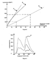
- the figure 3 details, for three sub-pixels of different colors, the luminance as a function of the current density.
- the curves G, R and B represent the evolution of the luminance as a function of the current density for a diode associated respectively with a green, red and blue filter.
- the luminance obtained for a frame time of 20 ms is 100 Cd / m 2 .
- the luminance being proportional to the duration of application of the current, it is sufficient to reduce the luminance to 100Cd / m 2 to apply the current only during a fraction of the frame time t namely: tx 100/250.
- the figure 4 represents the emission spectra of a diode which is fed at two current densities: 50 and 20 mA / cm 2 .
- the curves C and D represent the evolution of the luminance as a function of the wavelength of the emission spectrum respectively for current densities of 20 mA / cm 2 and 50 mA / cm 2 . If we compare the two emission spectra of the diode, we see that the proportion of energy emitted in the blue band, that is, between 450 and 495nm, relative to the total energy increases as the current density increases. The losses at the blue filter are therefore less important when the diode is polarized at 50 mA / cm 2 , curve D.
- the luminance of the blue sub-pixel is then greatly increased when its polarization density is increased.
- the selection criteria of the currents to be used are dictated by the chromatic coordinates that one wishes to obtain for the sub-pixel in question and by the luminance obtained after filtering.
- the following table gives, as a function of the polarization (the voltage / current pair), for the same diode, the luminance (in Cd / m 2 ) obtained after filtering as well as the chromatic coordinates (X, Y) in a diagram of CIE1931 chromacity, for a frame time t of 20ms.
- each diode is powered under conditions that favor obtaining a transmission spectrum that is close to the transmission spectrum of the associated color filter.
- the differences in light intensity of the diode that result from these polarization differences are modulated by the specific power times for each sub-pixel.
- each of the sub-pixels has the same luminance, here for example 100Cd / m 2 .
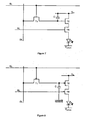
- the figure 5 illustrates an addressing circuit of a sub-pixel.
- a first transistor T1 operating as a switch, is connected by its control electrode (gate) to a selection line (SL), to select the diode, that is to say the sub-pixel, to activate.
- the first transistor T1 is connected between a data line (DL) and the control electrode of a second transistor T2.
- the transistor T1 When the transistor T1 is on (the subpixel is selected), the available voltage on the data line DL is available at the gate of the transistor T2.
- the transistor T2 and the diode 3 are connected in series and supplied between the supply voltage V dd and a predefined voltage V cathode .
- the transistor T2 is connected to the potential V dd while the diode is connected to the potential V cathode .
- the level of current flowing in the transistor and in the diode is set by the voltage level applied to the gate of transistor T2.
- this voltage is kept constant by a capacitor C which is arranged between the supply V dd and the gate of the transistor T2.
- the capacitor C is charged when the transistor T1 is in the on state.
- the pixel electrode that is to say the electrode which is controlled by the second transistor T2 corresponds to the anode of the light emitting diode.
- the cathode is in general common to all the pixels and the potential V cathode is fixed and constant.
- cathodes per color (a cathode for each color and for the entire display device). These cathodes are independent and it is possible to modulate the current or voltage across the various diodes driving these different cathodes.
- the anode of each sub-pixel then remains driven at a potential / current, for example constant, as in the prior art.
- This solution has the advantage of being able to maintain for the control circuit of the anode, at each sub-pixel, a circuit identical to the device of the prior art.
- control circuit sets, for each organic light emitting diode 3 of the pixel 1, the supply conditions (current and / or voltage) that allow optimal light output with the corresponding color filter 4.
- the fixed control circuit for example for each organic light emitting diode 3 of the pixel 1, a current which defines the color emitted by the diode and also its instantaneous luminance.
- the polarization of the diode Since the polarization of the diode has been chosen to optimize the emitted color, the luminance obtained is brought back to the required luminance by varying the application time of this polarization: the diode is no longer supplied during the entire frame time t.
- the addressing circuit of the diode 3 comprises means for controlling the duration of application of the supply voltage and / or the supply current depending on the color of the sub-pixel.
- the addressing circuit of the diode comprises a control transistor T3, operating as a switch, connected between the control electrode (gate) of the second transistor T2 and the terminal of the power source connected to the diode, preferably, the mass.
- the control electrode (gate) of the control transistor T3 is connected to a reset line (RL) which constitutes with the control transistor T2 means for controlling the duration of application of the current through the diode 3.
- the transistor T3 When the transistor T3 is off, the voltage on the gate of the transistor T2 is maintained thanks to the capacitor C and the desired current flows in the diode 3.
- the capacitor C discharges and the potential of the terminal the power source connected to the diode (preferably the ground) is returned to the gate of the transistor T2, blocking the transistor T2: no current then flows in the diode.
- the reset line (RL) and the control transistor T3 thus make it possible to set, during each frame period ⁇ t, a maximum duration during which the diode is energized.
- the control means of the duration of application of the supply conditions makes it possible to modulate, on the frame time, the average luminance of each sub-pixel, that is to say that they make it possible to obtain an average luminance predetermined for a predetermined period.
- the control circuit periodically sets, for a frame period ⁇ t, for example 20 ms, the chromatic coordinates of the pixel 1 and its luminance by modulating the luminances of the sub-pixels.
- ⁇ t for example 20 ms
- the control circuit selects the sub-pixels 2 necessary to obtain the chromatic coordinates of the pixel and controls the luminance of each of these sub-pixels 2.
- the control transistors T3 associated with sub-pixels of different colors are conductive for durations t on which depend on this color (t on ⁇ ⁇ t) during each period ⁇ t.
- the duration takes into account the differences in instantaneous luminance existing between the different sub-pixels of the same pixel because of the differences in their voltage and / or supply current.
- the control circuit controls the period t power on each of the sub-pixels 2.
- the application time t on of the supply voltage or the supply current can be adjusted by the anode or the cathode.
- the addressing circuit illustrated in FIG. figure 5 and which cooperates with the control circuit has been realized using n-type transistors, but similarly, a circuit could be made from a p-type transistor as shown in FIG. figure 6 .
- the transistor T3 may be arranged in series with the diode for, in the off state, to block the current flowing in the diode. It could also be mounted in parallel with the capacity.
- the diode 3 associated with the red filter is polarized with a lower current than the other sub-pixels to obtain the maximum emission efficiency in the red band.
- a luminance of the red sub-pixel which is comparable to that of the other sub-pixels, it is chosen to polarize the diode for a longer time, for example, during the entire frame period ⁇ t.
- the diode 3 associated with the blue filter is biased with a current stronger than the other sub-pixels to obtain the maximum emission efficiency in the blue band, it can be polarized for a shorter time.
- the product of the instantaneous luminance L of the diode by its duration of supply (Lxt on ) corresponds to the average luminance of the sub-pixel over the period ⁇ t.
- the overall luminance of pixel 1 then depends on the average luminance of the different selected subpixels.
- the voltage or the supply current of each of the organic electroluminescent diodes 3 being fixed as a function of the color of the corresponding sub-pixel (V R , V G , V B or I R , I B , I G ), the the color of the pixel 1 and its luminance are determined by the control circuit by selection of the appropriate sub-pixels (SL command of the figure 3 ) and modulation of the supply duration t on each of the sub-pixels 2 of color.
- each color sub-pixel 2 may be constituted by a single pulse whose duration (t on ) in the high state is set by the signals RL of the control circuit.
- the invention is not limited to the embodiments described above.
- the addressing circuit of the Figures 5 to 8 can be replaced by any circuit for adapting the voltage and / or the supply current of a color sub-pixel so that its emission spectrum is close to the transmission spectrum of the color filter of the sub-pixel, and to adapt the diode supply time t on the color of the sub-pixel, to obtain a predetermined average luminance for a predetermined period ⁇ t.
- the display device also comprises an addressing circuit specific to each sub-pixel 2 in order to select the desired sub-pixel 2 and to control its duration of supply and its supply conditions.
- This specific addressing circuit may be that represented, for example, Figures 5 to 8 .
- the display device comprises, as before, a control circuit which cooperates with the different addressing circuits of the pixel array 1 to obtain the desired image, both in terms of colors and gray levels.
- the control circuit manages all the sub-pixels 2 of the matrix in order to emit the desired image.
- Each sub-pixel addressing circuit 2 has a reset terminal which controls the sub-pixel 2 power-up time, i.e. the power-on time of the light-emitting element. 3.
- Each addressing circuit also includes a selection terminal which makes it possible to define whether the light emitter 3 of the sub-pixel 2 must be powered or not. current.
- Each addressing circuit further comprises a power control terminal which makes it possible to modulate the supply conditions of the sub-pixel 2.
- the cathode may be common to sub-pixels of a given color, therefore to a group of sub-pixels 2, or the cathode may be specific to each sub-pixel 2.
- the selection input of the sub-pixel 2 may be constituted by the control terminal of a first transistor T1.
- the first transistor T1 is in an on or off state which has the effect of allowing or not the passage of a current in the light emitter 3 of the sub-pixel 2 .
- the control input of the supply conditions of the sub-pixel 2 may be constituted by an input terminal of the first transistor T1 whose output terminal is connected to the control terminal of the second transistor T2.
- the second transistor T2 modulates the amount of current that can be applied to the light emitter 3.
- the modulation of the current in the transmitter of light 3 is effective only if the first transistor T1 is in an on state.
- the reset input of the sub-pixel 2 may be constituted by the control terminal of the third transistor T3 which is connected between the control terminal of the second transistor T2 and the ground or the supply voltage V dd . In this way, depending on the voltage applied to the control terminal of the third transistor T3, the second transistor T2 is in a blocked or on state.
- the different addressing circuits associated with a sub-pixel color 2, that is to say to a colored filter color 4 are connected to the same reset line RL.
- the control circuit is connected to all the sub-pixels 2 via their respective addressing circuit.
- the control circuit is connected independently to each sub-pixel 2 by a specific selection line SL and by a control line of the specific supply conditions DL.
- the control circuit is also connected to the different sub-pixels 2 by reset lines RL which set the duration of power supply t on the sub-pixel 2.
- reset lines are specific to a color of sub-pixel 2.
- the control circuit has as many RL reset lines as there are sub-pixels 2 of different colors in a pixel 1.
- the control circuit has as many selection lines SL and control lines of the power conditions DL as subpixels 2 in the matrix. In this way, it is possible to reduce the amount of independent lines in the display device, while ensuring independence of use of different sub-pixels 2 and an increase in energy performance.
- the reset line RL can be physically common to all sub pixels of the same color. This may be the case for example, when the reset line is connected to the anode or the cathode of a diode.
- the first transistor T1 is connected between the control line of the supply conditions DL and the control electrode of the second transistor T2.
- the diode 3 of the sub-pixel 2 in question is connected in series with the second transistor T2 between the supply voltage V dd and the predefined potential of the cathode V cathode .
- the capacitor C and the third transistor T3 are connected in series between the supply voltage V dd and the ground.
- the common terminal of the capacitor C and the third transistor T3 is connected to the control terminal of the second transistor T2 and to the first transistor T1.
- the reset line RL is connected to an electrode of control of the third transistor T3.
- the control terminal of the first transistor T1 is connected to the selection line SL.
- the first transistor T1 is connected between the control line of the supply conditions DL and the control electrode of the second transistor T2.
- the diode 3 of the sub-pixel 2 in question is connected in series with the second T2 and third T3 transistors between the supply voltage V dd and the predefined potential applied to the cathode V cathode .
- the capacitor C is connected between the supply voltage V dd and the control terminal of the second transistor T2 or between the ground and the control terminal of the second transistor T2.
- the reset line RL is connected to the control electrode of the third transistor T3.
- the control terminal of the first transistor T1 is connected to the selection line SL. In this case, the relative position of the second T2 and third T3 transistors between the diode and the supply voltage Vdd is not important.
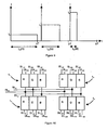
- the matrix of pixels 1 comprises four pixels 1 1 , 1 2 , 1 3 and 1 4 which each consist of three sub-pixels 2 called blue "B", green "G” and red “R".
- the control circuit comprises a single reset line RL R associated with the red subpixels, a single reset line RL G associated with the green subpixels and a single reset line RL B associated with the sub-pixels. blue pixels.
- the control circuit also has as many selection lines as subpixels (here twelve selection lines SL 1 -SL 12 ) and as many control lines as subpixels (here twelve control lines DL 1 -DL 12 )
- the reset line RL controlling the duration of supply of the sub-pixels 2 of the same color, all the red sub-pixels are fed during a first predetermined duration t on (R) , all the green sub-pixels are fed for a predetermined second time t on (G) and all Blue sub-pixels are fed for a third predetermined duration t on (B) .
- the different sub-pixels 2 are fed with the proviso that the first transistor T1 is in an on state, that is, they have been selected to emit light. In this way, a sub-pixel 2 is fed if the information on its selection line SL authorizes it and the sub-pixel 2 is then fed only for the duration which is defined by the reset line RL .
- the modulation of the luminance of each sub-pixel 2 and thus of the pixel 1 is carried out by modulating the supply voltage at the terminals of each sub-pixel 2. Indeed, as has been previously stated according to the supply conditions of each diode 3, there is modulation of the emitted color, but also of the instantaneous luminance. There is therefore for a given supply condition, a color and a luminance instant predefined. As a result, the modulation of the luminance for a given color is achieved by modulating for each of the sub-pixels 2 the supply conditions.
- Each sub-pixel 2 naturally remains fed in a range such that the emitted color is close to that of the associated colored filter 4 so as to maintain an energetic interest in this architecture.
- the color emitted by the sub-pixel 2 is defined by the intersection between the transmission spectrum of the color filter and the emission spectrum of the light-emitting element 3.
- a display device comprising this control circuit associated with a plurality of identical pixels 1 with variable chromaticity coordinates with sub-pixels 2 and their associated addressing circuit, the operating conditions are fixed in the following manner.
- each sub-pixel 2 (each light emitter 3) is supplied under different conditions in order to determine the most favorable energy supply conditions with the color filter 4 In this way, the light emitter 3 of each sub-pixel 2 has a transmission spectrum that is as close as possible to the transmission spectrum of the transmission spectrum of the associated color filter.
- each sub-pixel 2 According to the power conditions selected for each sub-pixel 2, the latter present between them different instantaneous luminances.
- Each sub-pixel 2 is then supplied with a specific predetermined duration so that the corresponding pixel 1 emits a predetermined color and luminance.
- the feed times of each of the sub-pixels are chosen so that the pixel emits a white color under the most favorable supply conditions between each light emitter 3 and the color filter 4 associated with it. .
- each sub-pixel is powered under different conditions (voltage and / or current).
- the modulation of the characteristics of the radiation emitted by the pixel is achieved by modulating the power conditions of the sub-pixels that compose it.
- the cathode is common to all the sub-pixels of the same color, it is then possible to realize control of the feeding time by means of the cathode.
- the reset line is made by the cathode common to all the sub-pixels of the same color. This discount zero results in the appearance of a potential difference lower than a threshold voltage at the terminals of the diode 3. Indeed, it must be considered that the control voltage of the anode can vary depending on the level displayed, it is not necessary to can not guarantee a constant voltage across the diode. The use of a threshold voltage is then very advantageous.
- the second transistor T2 it is possible to independently control the supply conditions of each of the diodes by means of the second transistor T2.
- the pixel electrode represents the cathode of the light-emitting diode
- the third transistor T3 can be eliminated.
Landscapes
- Engineering & Computer Science (AREA)
- Physics & Mathematics (AREA)
- Computer Hardware Design (AREA)
- General Physics & Mathematics (AREA)
- Theoretical Computer Science (AREA)
- Control Of Indicators Other Than Cathode Ray Tubes (AREA)
- Electroluminescent Light Sources (AREA)
- Control Of El Displays (AREA)
Applications Claiming Priority (2)
| Application Number | Priority Date | Filing Date | Title |
|---|---|---|---|
| FR0802584A FR2931296B1 (fr) | 2008-05-13 | 2008-05-13 | Circuit de controle d'un pixel a coordonnees chromatiques variables |
| PCT/FR2009/000533 WO2009141530A1 (fr) | 2008-05-13 | 2009-05-06 | Dispositif d'affichage amélioré à base de pixels à coordonnées chromatiques variables |
Publications (2)
| Publication Number | Publication Date |
|---|---|
| EP2277164A1 EP2277164A1 (fr) | 2011-01-26 |
| EP2277164B1 true EP2277164B1 (fr) | 2015-10-14 |
Family
ID=39921646
Family Applications (1)
| Application Number | Title | Priority Date | Filing Date |
|---|---|---|---|
| EP09750011.0A Active EP2277164B1 (fr) | 2008-05-13 | 2009-05-06 | Dispositif d'affichage amélioré à base de pixels à coordonnées chromatiques variables |
Country Status (6)
| Country | Link |
|---|---|
| US (1) | US8749596B2 (ko) |
| EP (1) | EP2277164B1 (ko) |
| JP (1) | JP5490784B2 (ko) |
| KR (1) | KR101614174B1 (ko) |
| FR (1) | FR2931296B1 (ko) |
| WO (1) | WO2009141530A1 (ko) |
Families Citing this family (9)
| Publication number | Priority date | Publication date | Assignee | Title |
|---|---|---|---|---|
| US8849345B2 (en) | 2011-09-29 | 2014-09-30 | Samsung Electro-Mechanics Co., Ltd. | Apparatus and method for super high-speed wireless communications |
| US9666119B2 (en) | 2012-08-30 | 2017-05-30 | Apple Inc. | Systems and methods for controlling current in display devices |
| JP6192431B2 (ja) * | 2013-08-21 | 2017-09-06 | 株式会社ジャパンディスプレイ | 有機el表示装置の駆動方法、及び有機el表示装置 |
| CN105679803B (zh) * | 2016-03-25 | 2018-01-05 | 北京京东方显示技术有限公司 | 显示面板及其控制方法、显示装置、显示系统 |
| KR20180038112A (ko) * | 2016-10-05 | 2018-04-16 | 삼성디스플레이 주식회사 | 헤드 마운티드 디스플레이 장치 |
| KR102527793B1 (ko) * | 2017-10-16 | 2023-05-04 | 삼성디스플레이 주식회사 | 표시 장치 및 그 구동 방법 |
| KR102523646B1 (ko) | 2017-11-01 | 2023-04-21 | 삼성디스플레이 주식회사 | 표시 장치 및 그 구동 방법 |
| US10950167B1 (en) * | 2019-10-17 | 2021-03-16 | Solomon Systech (Shenzhen) Limited | LED display with electroluminescent components |
| WO2023106049A1 (ja) * | 2021-12-10 | 2023-06-15 | ソニーグループ株式会社 | 表示装置および電子機器 |
Family Cites Families (24)
| Publication number | Priority date | Publication date | Assignee | Title |
|---|---|---|---|---|
| US3683365A (en) * | 1970-04-06 | 1972-08-08 | Robertshaw Controls Co | Alphanumeric message readout circuit |
| JPH08321380A (ja) * | 1995-05-25 | 1996-12-03 | Chisso Corp | 有機電界発光素子 |
| US5773130A (en) * | 1996-06-06 | 1998-06-30 | Motorola, Inc. | Multi-color organic electroluminescent device |
| WO1998059382A1 (en) * | 1997-06-23 | 1998-12-30 | Fed Corporation | Voltage controlled color organic light emitting device and method of producing the same |
| US20010030511A1 (en) * | 2000-04-18 | 2001-10-18 | Shunpei Yamazaki | Display device |
| JP2004145300A (ja) * | 2002-10-03 | 2004-05-20 | Seiko Epson Corp | 電子回路、電子回路の駆動方法、電子装置、電気光学装置、電気光学装置の駆動方法及び電子機器 |
| AU2003276706A1 (en) * | 2002-10-31 | 2004-05-25 | Casio Computer Co., Ltd. | Display device and method for driving display device |
| JP2005091420A (ja) * | 2003-09-12 | 2005-04-07 | Sony Corp | 表示装置およびその制御方法 |
| JP4731865B2 (ja) * | 2003-10-03 | 2011-07-27 | 株式会社半導体エネルギー研究所 | 発光装置 |
| GB0400209D0 (en) * | 2004-01-07 | 2004-02-11 | Koninkl Philips Electronics Nv | Light emitting display devices |
| US7595796B2 (en) | 2004-04-23 | 2009-09-29 | Hewlett-Packard Development Company, L.P. | Optimizing lifetime of a display |
| KR101121617B1 (ko) * | 2004-04-29 | 2012-02-28 | 엘지디스플레이 주식회사 | 일렉트로-루미네센스 표시장치 |
| TWI267822B (en) * | 2004-04-30 | 2006-12-01 | Fuji Photo Film Co Ltd | Organic electroluminescence device that can adjust chromaticity |
| JP4846999B2 (ja) * | 2004-10-20 | 2011-12-28 | 株式会社 日立ディスプレイズ | 画像表示装置 |
| KR100675939B1 (ko) * | 2005-09-14 | 2007-02-02 | 비오이 하이디스 테크놀로지 주식회사 | 유기 전계발광 표시장치 |
| EP1770676B1 (en) * | 2005-09-30 | 2017-05-03 | Semiconductor Energy Laboratory Co., Ltd. | Display device and electronic device |
| DE102005059765A1 (de) * | 2005-12-14 | 2007-06-21 | Patent-Treuhand-Gesellschaft für elektrische Glühlampen mbH | Anzeigevorrichtung mit einer Vielzahl von Bildpunkten und Verfahren zum Anzeigen von Bildern |
| US7332860B2 (en) * | 2006-03-30 | 2008-02-19 | Eastman Kodak Company | Efficient white-light OLED display with filters |
| TW200818979A (en) * | 2006-09-29 | 2008-04-16 | Osram Opto Semiconductors Gmbh | Organic light-emitting component, device with the same, lighting equipment and display device |
| KR101320021B1 (ko) * | 2006-10-17 | 2013-10-18 | 삼성디스플레이 주식회사 | 백라이트용 광원 및 백라이트 어셈블리 그리고 이를포함하는 액정 표시 장치 |
| KR101359632B1 (ko) * | 2007-01-19 | 2014-02-19 | 삼성디스플레이 주식회사 | 백색 유기 발광 소자 |
| KR20080101679A (ko) * | 2007-05-18 | 2008-11-21 | 소니 가부시끼 가이샤 | 표시 장치, 영상 신호 처리 방법, 및 프로그램 |
| US8063552B2 (en) * | 2007-10-22 | 2011-11-22 | Global Oled Technology Llc | LED device having improved light output |
| US8269212B2 (en) * | 2009-04-29 | 2012-09-18 | Honeywell International Inc. | OLED display with a common anode and method for forming the same |
-
2008
- 2008-05-13 FR FR0802584A patent/FR2931296B1/fr not_active Expired - Fee Related
-
2009
- 2009-05-06 WO PCT/FR2009/000533 patent/WO2009141530A1/fr active Application Filing
- 2009-05-06 US US12/988,657 patent/US8749596B2/en active Active
- 2009-05-06 JP JP2011508969A patent/JP5490784B2/ja active Active
- 2009-05-06 EP EP09750011.0A patent/EP2277164B1/fr active Active
- 2009-05-06 KR KR1020107025365A patent/KR101614174B1/ko active IP Right Grant
Also Published As
| Publication number | Publication date |
|---|---|
| WO2009141530A1 (fr) | 2009-11-26 |
| FR2931296A1 (fr) | 2009-11-20 |
| FR2931296B1 (fr) | 2013-04-26 |
| EP2277164A1 (fr) | 2011-01-26 |
| JP5490784B2 (ja) | 2014-05-14 |
| JP2011523467A (ja) | 2011-08-11 |
| US8749596B2 (en) | 2014-06-10 |
| US20110037791A1 (en) | 2011-02-17 |
| KR101614174B1 (ko) | 2016-04-20 |
| KR20110007182A (ko) | 2011-01-21 |
Similar Documents
| Publication | Publication Date | Title |
|---|---|---|
| EP2277164B1 (fr) | Dispositif d'affichage amélioré à base de pixels à coordonnées chromatiques variables | |
| EP1644913B1 (fr) | Dispositif d'affichage et circuit de commande d'un modulateur de lumiere | |
| JP4087844B2 (ja) | フォトルミネセンスを減少するためのエレクトロルミネセンス・ディスプレイ及びドライバ回路 | |
| EP3649672B1 (fr) | Dispositif d'affichage a leds | |
| US7053412B2 (en) | Grey scale bistable display | |
| US7456827B2 (en) | Active matrix display with variable duty cycle | |
| EP2628150A1 (fr) | Ecran d'affichage a diodes electroluminescentes a matrice active pourvu de moyens d'attenuation | |
| WO2005059883A2 (fr) | Cellule de commande electronique pour diode electroluminescente organique d'afficheur a matrice active, procedes de fonctionnement et afficheur | |
| KR20050083888A (ko) | 능동 매트릭스 전자발광 디스플레이를 위한 컬러 제어 | |
| EP1700290B1 (fr) | Ecran d'affichage d'images et procede d'adressage de cet ecran | |
| EP2997566B1 (fr) | Dispositif electrooptique a matrice de pixels de grande dimension | |
| EP1864275B1 (fr) | Dispositif d'affichage d'images et procede de pilotage de celui-ci. | |
| US7227304B2 (en) | Image display apparatus | |
| EP1771838B1 (fr) | Dispositif d'affichage d'images et procede de commande d'un dispositif d'affichage | |
| FR2766602A1 (fr) | Agencement de commande de cellule d'un affichage a emission de champs | |
| FR2846794A1 (fr) | Panneau organique electroluminescent bi-stable ou chaque cellule comprend une diode de shockley | |
| JP2007508594A (ja) | カラーディスプレイパネル | |
| WO2023110604A1 (fr) | Pixel d'affichage a diodes electroluminescentes pour ecran d'affichage | |
| Miller et al. | LED Display Technologies | |
| WO2023117605A1 (fr) | Ecran d'affichage comprenant des pixels d'affichage a diodes electroluminescentes | |
| JP2024513762A (ja) | マイクロ発光ダイオードディスプレイのためのベースラインおよび整形パルス駆動 |
Legal Events
| Date | Code | Title | Description |
|---|---|---|---|
| PUAI | Public reference made under article 153(3) epc to a published international application that has entered the european phase |
Free format text: ORIGINAL CODE: 0009012 |
|
| 17P | Request for examination filed |
Effective date: 20101108 |
|
| AK | Designated contracting states |
Kind code of ref document: A1 Designated state(s): AT BE BG CH CY CZ DE DK EE ES FI FR GB GR HR HU IE IS IT LI LT LU LV MC MK MT NL NO PL PT RO SE SI SK TR |
|
| AX | Request for extension of the european patent |
Extension state: AL BA RS |
|
| RIN1 | Information on inventor provided before grant (corrected) |
Inventor name: BILLOINT, OLIVIER Inventor name: VAUFREY, DAVID Inventor name: HAAS, GUNTHER |
|
| DAX | Request for extension of the european patent (deleted) | ||
| 17Q | First examination report despatched |
Effective date: 20110815 |
|
| REG | Reference to a national code |
Ref country code: DE Ref legal event code: R079 Ref document number: 602009034226 Country of ref document: DE Free format text: PREVIOUS MAIN CLASS: G09G0003320000 Ipc: G09G0003200000 |
|
| RIC1 | Information provided on ipc code assigned before grant |
Ipc: G09G 3/32 20060101ALI20111031BHEP Ipc: G09G 3/20 20060101AFI20111031BHEP |
|
| GRAP | Despatch of communication of intention to grant a patent |
Free format text: ORIGINAL CODE: EPIDOSNIGR1 |
|
| INTG | Intention to grant announced |
Effective date: 20150511 |
|
| GRAS | Grant fee paid |
Free format text: ORIGINAL CODE: EPIDOSNIGR3 |
|
| GRAA | (expected) grant |
Free format text: ORIGINAL CODE: 0009210 |
|
| AK | Designated contracting states |
Kind code of ref document: B1 Designated state(s): AT BE BG CH CY CZ DE DK EE ES FI FR GB GR HR HU IE IS IT LI LT LU LV MC MK MT NL NO PL PT RO SE SI SK TR |
|
| REG | Reference to a national code |
Ref country code: GB Ref legal event code: FG4D Free format text: NOT ENGLISH |
|
| REG | Reference to a national code |
Ref country code: AT Ref legal event code: REF Ref document number: 755647 Country of ref document: AT Kind code of ref document: T Effective date: 20151015 Ref country code: CH Ref legal event code: EP |
|
| REG | Reference to a national code |
Ref country code: IE Ref legal event code: FG4D Free format text: LANGUAGE OF EP DOCUMENT: FRENCH |
|
| REG | Reference to a national code |
Ref country code: DE Ref legal event code: R096 Ref document number: 602009034226 Country of ref document: DE |
|
| REG | Reference to a national code |
Ref country code: NL Ref legal event code: MP Effective date: 20151014 |
|
| REG | Reference to a national code |
Ref country code: LT Ref legal event code: MG4D |
|
| REG | Reference to a national code |
Ref country code: AT Ref legal event code: MK05 Ref document number: 755647 Country of ref document: AT Kind code of ref document: T Effective date: 20151014 |
|
| PG25 | Lapsed in a contracting state [announced via postgrant information from national office to epo] |
Ref country code: IS Free format text: LAPSE BECAUSE OF FAILURE TO SUBMIT A TRANSLATION OF THE DESCRIPTION OR TO PAY THE FEE WITHIN THE PRESCRIBED TIME-LIMIT Effective date: 20160214 Ref country code: HR Free format text: LAPSE BECAUSE OF FAILURE TO SUBMIT A TRANSLATION OF THE DESCRIPTION OR TO PAY THE FEE WITHIN THE PRESCRIBED TIME-LIMIT Effective date: 20151014 Ref country code: LT Free format text: LAPSE BECAUSE OF FAILURE TO SUBMIT A TRANSLATION OF THE DESCRIPTION OR TO PAY THE FEE WITHIN THE PRESCRIBED TIME-LIMIT Effective date: 20151014 Ref country code: ES Free format text: LAPSE BECAUSE OF FAILURE TO SUBMIT A TRANSLATION OF THE DESCRIPTION OR TO PAY THE FEE WITHIN THE PRESCRIBED TIME-LIMIT Effective date: 20151014 Ref country code: NL Free format text: LAPSE BECAUSE OF FAILURE TO SUBMIT A TRANSLATION OF THE DESCRIPTION OR TO PAY THE FEE WITHIN THE PRESCRIBED TIME-LIMIT Effective date: 20151014 Ref country code: NO Free format text: LAPSE BECAUSE OF FAILURE TO SUBMIT A TRANSLATION OF THE DESCRIPTION OR TO PAY THE FEE WITHIN THE PRESCRIBED TIME-LIMIT Effective date: 20160114 |
|
| REG | Reference to a national code |
Ref country code: FR Ref legal event code: PLFP Year of fee payment: 8 |
|
| PG25 | Lapsed in a contracting state [announced via postgrant information from national office to epo] |
Ref country code: PL Free format text: LAPSE BECAUSE OF FAILURE TO SUBMIT A TRANSLATION OF THE DESCRIPTION OR TO PAY THE FEE WITHIN THE PRESCRIBED TIME-LIMIT Effective date: 20151014 Ref country code: PT Free format text: LAPSE BECAUSE OF FAILURE TO SUBMIT A TRANSLATION OF THE DESCRIPTION OR TO PAY THE FEE WITHIN THE PRESCRIBED TIME-LIMIT Effective date: 20160215 Ref country code: SE Free format text: LAPSE BECAUSE OF FAILURE TO SUBMIT A TRANSLATION OF THE DESCRIPTION OR TO PAY THE FEE WITHIN THE PRESCRIBED TIME-LIMIT Effective date: 20151014 Ref country code: GR Free format text: LAPSE BECAUSE OF FAILURE TO SUBMIT A TRANSLATION OF THE DESCRIPTION OR TO PAY THE FEE WITHIN THE PRESCRIBED TIME-LIMIT Effective date: 20160115 Ref country code: LV Free format text: LAPSE BECAUSE OF FAILURE TO SUBMIT A TRANSLATION OF THE DESCRIPTION OR TO PAY THE FEE WITHIN THE PRESCRIBED TIME-LIMIT Effective date: 20151014 Ref country code: FI Free format text: LAPSE BECAUSE OF FAILURE TO SUBMIT A TRANSLATION OF THE DESCRIPTION OR TO PAY THE FEE WITHIN THE PRESCRIBED TIME-LIMIT Effective date: 20151014 Ref country code: AT Free format text: LAPSE BECAUSE OF FAILURE TO SUBMIT A TRANSLATION OF THE DESCRIPTION OR TO PAY THE FEE WITHIN THE PRESCRIBED TIME-LIMIT Effective date: 20151014 |
|
| REG | Reference to a national code |
Ref country code: DE Ref legal event code: R097 Ref document number: 602009034226 Country of ref document: DE |
|
| PG25 | Lapsed in a contracting state [announced via postgrant information from national office to epo] |
Ref country code: CZ Free format text: LAPSE BECAUSE OF FAILURE TO SUBMIT A TRANSLATION OF THE DESCRIPTION OR TO PAY THE FEE WITHIN THE PRESCRIBED TIME-LIMIT Effective date: 20151014 |
|
| PLBE | No opposition filed within time limit |
Free format text: ORIGINAL CODE: 0009261 |
|
| STAA | Information on the status of an ep patent application or granted ep patent |
Free format text: STATUS: NO OPPOSITION FILED WITHIN TIME LIMIT |
|
| PG25 | Lapsed in a contracting state [announced via postgrant information from national office to epo] |
Ref country code: EE Free format text: LAPSE BECAUSE OF FAILURE TO SUBMIT A TRANSLATION OF THE DESCRIPTION OR TO PAY THE FEE WITHIN THE PRESCRIBED TIME-LIMIT Effective date: 20151014 Ref country code: SK Free format text: LAPSE BECAUSE OF FAILURE TO SUBMIT A TRANSLATION OF THE DESCRIPTION OR TO PAY THE FEE WITHIN THE PRESCRIBED TIME-LIMIT Effective date: 20151014 Ref country code: DK Free format text: LAPSE BECAUSE OF FAILURE TO SUBMIT A TRANSLATION OF THE DESCRIPTION OR TO PAY THE FEE WITHIN THE PRESCRIBED TIME-LIMIT Effective date: 20151014 Ref country code: BE Free format text: LAPSE BECAUSE OF NON-PAYMENT OF DUE FEES Effective date: 20160531 Ref country code: RO Free format text: LAPSE BECAUSE OF FAILURE TO SUBMIT A TRANSLATION OF THE DESCRIPTION OR TO PAY THE FEE WITHIN THE PRESCRIBED TIME-LIMIT Effective date: 20151014 |
|
| 26N | No opposition filed |
Effective date: 20160715 |
|
| PG25 | Lapsed in a contracting state [announced via postgrant information from national office to epo] |
Ref country code: SI Free format text: LAPSE BECAUSE OF FAILURE TO SUBMIT A TRANSLATION OF THE DESCRIPTION OR TO PAY THE FEE WITHIN THE PRESCRIBED TIME-LIMIT Effective date: 20151014 |
|
| PG25 | Lapsed in a contracting state [announced via postgrant information from national office to epo] |
Ref country code: LU Free format text: LAPSE BECAUSE OF FAILURE TO SUBMIT A TRANSLATION OF THE DESCRIPTION OR TO PAY THE FEE WITHIN THE PRESCRIBED TIME-LIMIT Effective date: 20160506 |
|
| REG | Reference to a national code |
Ref country code: CH Ref legal event code: PL |
|
| PG25 | Lapsed in a contracting state [announced via postgrant information from national office to epo] |
Ref country code: LI Free format text: LAPSE BECAUSE OF NON-PAYMENT OF DUE FEES Effective date: 20160531 Ref country code: CH Free format text: LAPSE BECAUSE OF NON-PAYMENT OF DUE FEES Effective date: 20160531 |
|
| REG | Reference to a national code |
Ref country code: IE Ref legal event code: MM4A |
|
| REG | Reference to a national code |
Ref country code: FR Ref legal event code: PLFP Year of fee payment: 9 |
|
| PG25 | Lapsed in a contracting state [announced via postgrant information from national office to epo] |
Ref country code: IE Free format text: LAPSE BECAUSE OF NON-PAYMENT OF DUE FEES Effective date: 20160506 |
|
| REG | Reference to a national code |
Ref country code: FR Ref legal event code: PLFP Year of fee payment: 10 |
|
| PG25 | Lapsed in a contracting state [announced via postgrant information from national office to epo] |
Ref country code: CY Free format text: LAPSE BECAUSE OF FAILURE TO SUBMIT A TRANSLATION OF THE DESCRIPTION OR TO PAY THE FEE WITHIN THE PRESCRIBED TIME-LIMIT Effective date: 20151014 Ref country code: HU Free format text: LAPSE BECAUSE OF FAILURE TO SUBMIT A TRANSLATION OF THE DESCRIPTION OR TO PAY THE FEE WITHIN THE PRESCRIBED TIME-LIMIT; INVALID AB INITIO Effective date: 20090506 |
|
| PG25 | Lapsed in a contracting state [announced via postgrant information from national office to epo] |
Ref country code: MC Free format text: LAPSE BECAUSE OF FAILURE TO SUBMIT A TRANSLATION OF THE DESCRIPTION OR TO PAY THE FEE WITHIN THE PRESCRIBED TIME-LIMIT Effective date: 20151014 Ref country code: TR Free format text: LAPSE BECAUSE OF FAILURE TO SUBMIT A TRANSLATION OF THE DESCRIPTION OR TO PAY THE FEE WITHIN THE PRESCRIBED TIME-LIMIT Effective date: 20151014 Ref country code: MK Free format text: LAPSE BECAUSE OF FAILURE TO SUBMIT A TRANSLATION OF THE DESCRIPTION OR TO PAY THE FEE WITHIN THE PRESCRIBED TIME-LIMIT Effective date: 20151014 Ref country code: MT Free format text: LAPSE BECAUSE OF FAILURE TO SUBMIT A TRANSLATION OF THE DESCRIPTION OR TO PAY THE FEE WITHIN THE PRESCRIBED TIME-LIMIT Effective date: 20151014 |
|
| PG25 | Lapsed in a contracting state [announced via postgrant information from national office to epo] |
Ref country code: BG Free format text: LAPSE BECAUSE OF FAILURE TO SUBMIT A TRANSLATION OF THE DESCRIPTION OR TO PAY THE FEE WITHIN THE PRESCRIBED TIME-LIMIT Effective date: 20151014 |
|
| PGFP | Annual fee paid to national office [announced via postgrant information from national office to epo] |
Ref country code: IT Payment date: 20230531 Year of fee payment: 15 Ref country code: FR Payment date: 20230523 Year of fee payment: 15 Ref country code: DE Payment date: 20230519 Year of fee payment: 15 |
|
| PGFP | Annual fee paid to national office [announced via postgrant information from national office to epo] |
Ref country code: GB Payment date: 20230523 Year of fee payment: 15 |