EP2276110A1 - Radio device with a notch antenna - Google Patents
Radio device with a notch antenna Download PDFInfo
- Publication number
- EP2276110A1 EP2276110A1 EP10177550A EP10177550A EP2276110A1 EP 2276110 A1 EP2276110 A1 EP 2276110A1 EP 10177550 A EP10177550 A EP 10177550A EP 10177550 A EP10177550 A EP 10177550A EP 2276110 A1 EP2276110 A1 EP 2276110A1
- Authority
- EP
- European Patent Office
- Prior art keywords
- circuit substrate
- notch
- bent
- radio device
- antenna
- Prior art date
- Legal status (The legal status is an assumption and is not a legal conclusion. Google has not performed a legal analysis and makes no representation as to the accuracy of the status listed.)
- Withdrawn
Links
- 239000000758 substrate Substances 0.000 claims abstract description 76
- 230000001413 cellular effect Effects 0.000 claims description 23
- 238000005452 bending Methods 0.000 claims description 11
- 238000004891 communication Methods 0.000 claims description 11
- 230000000630 rising effect Effects 0.000 claims description 4
- 230000006866 deterioration Effects 0.000 abstract description 4
- 239000003989 dielectric material Substances 0.000 description 13
- 230000009467 reduction Effects 0.000 description 11
- 239000004020 conductor Substances 0.000 description 9
- 239000010410 layer Substances 0.000 description 9
- 238000005516 engineering process Methods 0.000 description 8
- 230000000694 effects Effects 0.000 description 6
- 230000015572 biosynthetic process Effects 0.000 description 4
- 238000004088 simulation Methods 0.000 description 4
- 239000003990 capacitor Substances 0.000 description 3
- 238000013461 design Methods 0.000 description 3
- RYGMFSIKBFXOCR-UHFFFAOYSA-N Copper Chemical compound [Cu] RYGMFSIKBFXOCR-UHFFFAOYSA-N 0.000 description 2
- 238000013459 approach Methods 0.000 description 2
- 229910052802 copper Inorganic materials 0.000 description 2
- 239000010949 copper Substances 0.000 description 2
- 230000006872 improvement Effects 0.000 description 2
- 238000003475 lamination Methods 0.000 description 2
- 230000005855 radiation Effects 0.000 description 2
- 238000005388 cross polarization Methods 0.000 description 1
- 238000010586 diagram Methods 0.000 description 1
- 239000003822 epoxy resin Substances 0.000 description 1
- 230000012447 hatching Effects 0.000 description 1
- 238000010348 incorporation Methods 0.000 description 1
- 239000004973 liquid crystal related substance Substances 0.000 description 1
- 238000005259 measurement Methods 0.000 description 1
- 238000012986 modification Methods 0.000 description 1
- 230000004048 modification Effects 0.000 description 1
- 230000005404 monopole Effects 0.000 description 1
- 229920000647 polyepoxide Polymers 0.000 description 1
- 229920005989 resin Polymers 0.000 description 1
- 239000011347 resin Substances 0.000 description 1
- 238000004904 shortening Methods 0.000 description 1
- 239000002356 single layer Substances 0.000 description 1
- 239000002344 surface layer Substances 0.000 description 1
Images


Classifications
-
- H—ELECTRICITY
- H01—ELECTRIC ELEMENTS
- H01Q—ANTENNAS, i.e. RADIO AERIALS
- H01Q1/00—Details of, or arrangements associated with, antennas
- H01Q1/36—Structural form of radiating elements, e.g. cone, spiral, umbrella; Particular materials used therewith
- H01Q1/38—Structural form of radiating elements, e.g. cone, spiral, umbrella; Particular materials used therewith formed by a conductive layer on an insulating support
-
- H—ELECTRICITY
- H01—ELECTRIC ELEMENTS
- H01Q—ANTENNAS, i.e. RADIO AERIALS
- H01Q1/00—Details of, or arrangements associated with, antennas
- H01Q1/12—Supports; Mounting means
- H01Q1/22—Supports; Mounting means by structural association with other equipment or articles
- H01Q1/24—Supports; Mounting means by structural association with other equipment or articles with receiving set
- H01Q1/241—Supports; Mounting means by structural association with other equipment or articles with receiving set used in mobile communications, e.g. GSM
- H01Q1/242—Supports; Mounting means by structural association with other equipment or articles with receiving set used in mobile communications, e.g. GSM specially adapted for hand-held use
- H01Q1/243—Supports; Mounting means by structural association with other equipment or articles with receiving set used in mobile communications, e.g. GSM specially adapted for hand-held use with built-in antennas
-
- H—ELECTRICITY
- H01—ELECTRIC ELEMENTS
- H01Q—ANTENNAS, i.e. RADIO AERIALS
- H01Q13/00—Waveguide horns or mouths; Slot antennas; Leaky-waveguide antennas; Equivalent structures causing radiation along the transmission path of a guided wave
- H01Q13/08—Radiating ends of two-conductor microwave transmission lines, e.g. of coaxial lines, of microstrip lines
- H01Q13/085—Slot-line radiating ends
-
- H—ELECTRICITY
- H01—ELECTRIC ELEMENTS
- H01Q—ANTENNAS, i.e. RADIO AERIALS
- H01Q13/00—Waveguide horns or mouths; Slot antennas; Leaky-waveguide antennas; Equivalent structures causing radiation along the transmission path of a guided wave
- H01Q13/10—Resonant slot antennas
- H01Q13/103—Resonant slot antennas with variable reactance for tuning the antenna
-
- H—ELECTRICITY
- H01—ELECTRIC ELEMENTS
- H01Q—ANTENNAS, i.e. RADIO AERIALS
- H01Q13/00—Waveguide horns or mouths; Slot antennas; Leaky-waveguide antennas; Equivalent structures causing radiation along the transmission path of a guided wave
- H01Q13/10—Resonant slot antennas
- H01Q13/106—Microstrip slot antennas
-
- H—ELECTRICITY
- H01—ELECTRIC ELEMENTS
- H01Q—ANTENNAS, i.e. RADIO AERIALS
- H01Q13/00—Waveguide horns or mouths; Slot antennas; Leaky-waveguide antennas; Equivalent structures causing radiation along the transmission path of a guided wave
- H01Q13/10—Resonant slot antennas
- H01Q13/16—Folded slot antennas
Definitions
- the present invention relates to a radio device and a cellular phone, and particularly to a radio device and a cellular phone with which it is possible to achieve a reduction in size and enhancement of antenna efficiency and gain.
- Patent Reference 1 As a technology for solving this problem, there have been made some proposals (see, for example, Patent References 1, 2, and 3 set forth below).
- the technology described in Patent Reference 1 is to physically prevent the hand of the user from covering the incorporated antenna portion by, for example, reducing the thickness of the casing surrounding the antenna.
- Patent Reference 2 ensures that the radiation direction of an incorporated antenna composed of any of a monopole antenna, an inverted F-type antenna, and a microstrip antenna avoids the side of the surface of the portable apparatus seated on a desk, thereby to render the antenna less susceptible to influences of the hands and metallic bodies and to improve the gain of the antenna.
- Patent Reference 3 in relation to an antenna composed of a radiating conductor and a ground conductor, is to dispose the ground conductor between the human head portion side and the radiating conductor, thereby reducing the radiation to the human head portion side and improving the gain of the antenna.
- Patent Reference 2 is effective in improvement of electric characteristics.
- the antenna characteristics may be deteriorated conspicuously, so that it is impossible to reduce the size of the area surrounding the antenna.
- Patent Reference 3 The technology of Patent Reference 3 is based on the assumption that the antenna portion is not covered by a hand, and the technology is an effective approach under the assumed condition. In practice, however, this approach restricts the way the terminal apparatus is held by the user's hand, which is inconvenient. Besides, when the antenna portion is covered with a hand, the radiating conductor is located between the hand and the ground conductor, possibly leading to a marked deterioration of gain.
- the present invention has been made in consideration of the above-mentioned problems involved in the prior art. Accordingly, it is an object of the present invention to provide a radio device with which it is possible to achieve a reduction in size and enhancement of antenna efficiency and gain.
- a radio device including a notch antenna, wherein the notch antenna comprises: a circuit substrate comprising a ground portion and a notch portion opened at one end thereof, and a radio circuit portion provided on the circuit substrate for supplying a high-frequency current to the notch portion.
- a conductive bent-back portion is formed so as to be connected to the ground portion and to extend the notch portion, on the one end side of the circuit substrate.
- the formation of the conductive bent-back portion which extends the notch portion leads to a reduction in the physical length of the notch portion functioning as a notch antenna, and also a reduction in the electrical length of the notch portion.
- the expression "a reduction in the electrical length of the notch portion” means that the formation of the bent-back portion provides the same effect as that obtained when a capacitor (capacitance) is interposed between the leading end of the bent-back portion and the circuit substrate, and, therefore, the substantial length of the notch portion is reduced. This makes it possible to reduce the size of the radio device and to enhance antenna efficiency.
- a cellular phone including: a casing; a circuit substrate incorporated in the casing and comprising a ground portion and a notch portion; a radio circuit portion provided on the circuit substrate for supplying a high-frequency current to the notch portion; and a conductive bent-back portion formed so as to be connected to the ground portion and to extend the notch portion, on one end side of the circuit substrate.
- the formation of the conductive bent-back portion which extends the notch portion leads to a reduction in the physical length of the notch portion functioning as a notch antenna, and also a reduction in the electrical length of the notch portion.
- the expression "a reduction in the electrical length of the notch portion” means that the formation of the notch portion produces the same effect as that obtained when a capacitor (capacitance) is interposed between the leading end of the bent-back portion and the circuit substrate, and, therefore, the substantial length of the notch portion is reduced. This makes it possible to reduce the size of the cellular phone and to enhance antenna efficiency.
- the "antenna efficiency" means the ratio of an RF signal radiated from the antenna to an RF signal radiated from the radio circuit portion. For example, the case where the RF signal radiated from the radio circuit portion is entirely radiated from the antenna corresponds to an antenna efficiency of 100%.
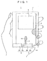
- a radio device 1 is a radio device in which a notch antenna is comprised of: a circuit substrate 4 comprising a ground portion 2 and a notch portion (slit) 3 opened at one end thereof; and a radio circuit portion 5 provided on the circuit substrate 4 for supplying a high-frequency current to the notch portion 3.
- the radio device 1 is incorporated in a casing 7 having such a size that it can be held on a hand 6, for example, and the radio device 1 is used as a radio device of a cellular phone.
- the circuit substrate 4 is provided with circuit portions (omitted in the figure) for respectively driving a liquid crystal display device, a speaker, a microphone and the like necessary for the cellular phone, and the ground portion 2.
- the ground portion 2 functions as a ground conductor (ground plate) of a notch antenna, is formed as one layer in the circuit substrate 4 having a multilayer circuit structure comprising a lamination of a plurality of layers, for example, and is formed on the whole substrate surface inclusive of bent-back portions 9 which will be described later.
- Figs. 1 and 2 are presented with a surface layer of the circuit substrate 4 being partly broken, and the ground portion 2 formed as a layer therebeneath is indicated by hatching. While the circuit substrate 4 in this embodiment has the multilayer circuit structure, a monolayer circuit substrate 4 may also be adopted, naturally.
- the circuit substrate 4 is provided with a notch portion 3 which operates as a notch antenna.
- the notch portion 3 is formed as an oblong rectangular slit formed to penetrate in the thickness direction of the circuit substrate 4.
- the notch portion 3 is formed to extend straight from an intermediate position of the circuit substrate 4 toward one end side, and to continue to the position of the bent-back portions 9 which are formed by bending back the one end side of the circuit substrate 4.
- the notch portion 3 has its notch opened at end portions of the bent-back portions 9.
- each of the bent-back portions 9 is formed by integrally bending a portion (one end side portion) of the circuit substrate 4.
- the bent-back portion 9 is bent back to the side opposite to the side of mounting on a hand (palm) 6.
- the bend-back portion 9 is comprised of: a perpendicular portion 9a rising to the side of one principal surface 4a of the circuit substrate 4 which is on the side opposite to the side of mounting on the hand 6 and on which a radio circuit portion 5 is formed; and a horizontal portion 9b extending from the leading end of the perpendicular portion 9a to the side of the radio circuit portion 5 (to the other end side of the circuit substrate 4).
- the perpendicular portion 9a rises substantially perpendicularly to the one principal surface 4a of the circuit substrate 4.
- the horizontal portion 9b extends substantially in parallel to the one principal surface 4a, from the leading end of the perpendicular portion 9a toward the side where the radio circuit portion 5 is provided.
- the bent-back portions 9 each comprised of the perpendicular portion 9a and the horizontal portion 9b are provided on one end side of the circuit substrate 4 in a roughly inverted L shape relative to the circuit substrate 4.
- the ground portion 2 is formed to continue to the positions of the leading ends of the bent-back portions 9.
- the radio circuit portion 5 is an RF circuit used in an ordinary cellular phone, and is a circuit for transmitting or receiving a high-frequency signal through the antenna.
- An RF signal from the radio circuit portion 5 is radiated from the notch portion 3, by supplying a current with a desired position of the notch portion 3 as a feeder portion 10 trough a feeder line which is omitted in the figures.
- the open end portion of the notch portion 3 which functions as a notch antenna is bent back, so that the antenna is less susceptible to the influence of the hand 6, resulting in that gain is enhanced.
- the whole length of the notch portion 3 inclusive of the bent-back portions 9 can be reduced both on a physical basis and on an electrical basis.
- 1/4 wavelength ( ⁇ ) of the wavelength ⁇ of a frequency used for the cellular phone is made to be the length of the notch portion 3, and the circuit substrate 4 is provided with a straight groove in a flat surface.
- the open end portion of the notch portion 3 is bent back, the length of the notch portion 3 is substantially reduced by an amount corresponding to the bent-back portion.
- the length of the notch portion 3 can be made substantially smaller than the length corresponding to 1/4 wavelength of the wavelength ⁇ of the frequency used for the cellular phone. Therefore, according to the radio device 1 in the first embodiment, it is possible to render the antenna smaller in size.
- a dielectric material in the notch portion 3 it may be contemplated to charge a dielectric material in the notch portion 3.
- the physical length of the notch portion 3 can be reduced owing to a wavelength-shortening effect of the dielectric material.
- the dielectric material is charged in the notch portion 3, however, there arises the problem that antenna efficiency is deteriorated.
- a simulation example of this problem is shown in Fig. 5 .
- Fig. 5 shows a radio device 15 in which a notch antenna is constituted by providing a circuit substrate 12 with crank-shaped notch portions 13 and filling the notch portions 13 with a dielectric material 14; in the figure, the portions where a loss is generated are indicated by contour lines 16. As seen from Fig. 5 , it is confirmed that the loss is generated at portions near the open ends in the dielectric material 14 charged in the notch portions 13 (the contour lines 16 are concentrated at the portions).
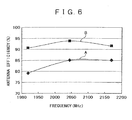
- FIG. 6 An example of simulation results relating to variations in antenna efficiency, in the case where the dielectric material 14 is charged in the notch portions 13 and in the case where the dielectric material 14 is not charged, is shown in Fig. 6 .
- line A corresponds to a radio device 15 in which a glass-epoxy resin as the dielectric material 14 is charged in the notch portions 13
- line B corresponds to the radio device 1 according to the first embodiment in which nothing is charged in the notch portion 13.
- the radio device 1 with nothing charged in the notch portion 3 shows an about 8% improvement in antenna efficiency, as compared to the radio device 15 with the dielectric material 14 charged in the notch portions 13.
- the radio device 1 according to the first embodiment was produced with a 2 GHz band, and gain measurement results at the time of talking in the case where the radio device 1 is incorporated in a casing on the side of key buttons of a cellular phone capable of being folded in two were examined.
- the object of comparison was a notch antenna in which the open end portion was not bent, and the differences in antenna efficiency were compensated, to compare only the amount of deterioration of gain due to the human body.
- the positional relationship between the bent antenna and the hand 6 of the testee is shown in Fig. 1 .
- the radio device 1 in the first embodiment by bending back the open end portion of the notch antenna it is possible to reduce the size of the antenna, and it is possible to enhance antenna efficiency with a simple structure. Furthermore, it is possible to reduce deterioration of gain due to the human hand holding the cellular phone or the like.
- a radio device 1 according to the second embodiment has a structure wherein a circuit substrate 4 has a multilayer structure, in which one layer is a flexible printed cable 17, and the flexible printed cable 17 is bent to form bent-back portions 9.
- the other points of constitution are the same as in the radio device 1 according to the first embodiment, so that the same components as those in the first embodiment are denoted by the same symbols as above, and description thereof is omitted.
- the circuit substrate 4 of the radio device 1 is a so-called multilayer substrate in which a plurality of wiring circuits 18a and 18b are formed in a lamination direction.
- one layer is the flexible printed cable 17.
- the flexible printed cable 17 is composed of a flexible cable, and, for example, has a conductive pattern of copper on the whole cable surface. On the conductive pattern, an insulating layer may be provided.
- the flexible printed cable 17 is bent to form the bent-back portions 9 at one end portion thereof.
- the flexible printed cable 17 is connected, on a high-frequency basis, to a ground portion 2 formed in the circuit substrate 4.
- the expression "connected, in a high-frequency basis” means that a high-frequency current is supplied from a radio circuit portion 5 to the flexible printed cable 17 through the ground portion 2.
- the flexible printed cable 17 is flexible, it is difficult for the bent-back portions 9 to maintain their shape by themselves; therefore, a form maintaining member (omitted in the figures) for forcibly maintaining the shape of the bent-back portions 9 is utilized.
- the form maintaining member is preferably formed of an insulating resin so that a short-circuit is not generated between the form maintaining member and a conductor formed on the flexible printed cable 17 or the like.
- the bent-back portions at the open end portion of the notch antenna are composed of the flexible printed cable 17, so that it is possible to realize a lighter weight and a lower cost, and to enhance the degree of freedom in design of the cellular phone.
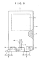
- a radio device 1 according to a third embodiment has a structure in which a metallic plate is bent to form bent-back portions 9, as shown in Fig. 9 .
- the other points of constitution are the same as in the radio device 1 according to the first embodiment, so that the same components as those in the first embodiment are denoted' by the same symbols as above, and description thereof is omitted.
- a metallic plate formed of a conductive material for example a copper plate, is bent to form the bent-back portions 9, in the same manner as in the radio device 1 according to the first embodiment.
- Each of the bent-back portions 9 comprises a perpendicular portion 9a and a horizontal portion 9b, in the same manner as in the radio device 1 according to the first embodiment, and additionally comprises a contact portion 9c for contact with a ground portion 2.
- the contact portion 9c is brought into close contact with the ground portion 2, and thereafter the bent-back portions 9 are fixed to a circuit substrate 4 by screws 19 for fixing both a casing 7 for containing the radio device 1 therein (the casing 7 is omitted in Fig. 9 ) and the circuit substrate 4. Since the bent-back portions 9 are fixed to the circuit substrate 4 by utilizing the screws 19 for fixing the casing 7 and the circuit substrate 4, the contact portions 9c can be fixed in close contact with the ground portion 2, to achieve grounding assuredly. Besides, since the bent-back portions 9 are fixed to the circuit substrate 4 by use of the screws 19 for fixing the casing 7 and the circuit substrate 4, it is possible to achieve a reduction in size of the mounting area.
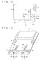
- a radio device 1 according to a fourth embodiment has a structure in which a metallic plate is bent to form a bent-back portion 9, the shape of the bent-back portion 9 being different from that in the radio device 1 according to the third embodiment.
- the other points of constitution are the same as in the radio device 1 according to the third embodiment, so that the same components as those in the third embodiment are denoted by the same symbols as above, and description thereof is omitted.
- the bent-back portion in the radio device 1 is comprised of: a perpendicular portion 9a rising substantially perpendicularly on the side of one principal surface 4a of a circuit substrate 4; a parallel portion 9b substantially parallel to the circuit substrate 4 and extending from the leading end of the perpendicular portion 9a in a direction substantially orthogonal to the notch direction of a notch portion 3 (the longitudinal direction of the slit); and a contact portion 9c for contact with a ground portion 2.
- the parallel portion 9b is formed as a flat plate having an oblong rectangular shape, and is formed to cross the notch portion 3.
- Fig. 12 is a plan view showing the bent-back portion 9 in a developed state.
- the notch portion 3 is formed in a roughly L shape in plan view, composed of a straight-shaped groove portion 3a formed in the circuit substrate 4, and a parallel groove portion 3b formed between one end 4a of the circuit substrate 4 and the parallel portion 9b.
- a notch antenna can be constituted by forming the bent-back portion 9 in this manner.
- a radio device 1 according to a fifth embodiment has a structure in which another bent-back portion 9 being the same as the bent-back portion 9 in the radio device 1 according to the fourth embodiment is additionally provided on the same circuit substrate 4, as shown in Fig. 13 .
- the radio device 1 according to the fifth embodiment is a radio device comprising two notch antennas on the circuit substrate 4.
- the present invention is not limited to the cellular phone, and the same functions or effects can be obtained when the invention is applied to, for example, a cordless phone, a hand-held PC, or a portable communication terminal device such as a PDA (Personal Digital Assistant) having a communication function.
- a cordless phone a hand-held PC
- a portable communication terminal device such as a PDA (Personal Digital Assistant) having a communication function.
- PDA Personal Digital Assistant
Landscapes
- Engineering & Computer Science (AREA)
- Computer Networks & Wireless Communication (AREA)
- Support Of Aerials (AREA)
- Telephone Set Structure (AREA)
- Details Of Aerials (AREA)
- Waveguide Aerials (AREA)
- Transceivers (AREA)
Applications Claiming Priority (2)
| Application Number | Priority Date | Filing Date | Title |
|---|---|---|---|
| JP2003001756A JP3912754B2 (ja) | 2003-01-08 | 2003-01-08 | 無線装置 |
| EP04000235A EP1437794A1 (en) | 2003-01-08 | 2004-01-08 | Radio device with a notch antenna |
Related Parent Applications (1)
| Application Number | Title | Priority Date | Filing Date |
|---|---|---|---|
| EP04000235.4 Division | 2004-01-08 |
Publications (1)
| Publication Number | Publication Date |
|---|---|
| EP2276110A1 true EP2276110A1 (en) | 2011-01-19 |
Family
ID=32501201
Family Applications (2)
| Application Number | Title | Priority Date | Filing Date |
|---|---|---|---|
| EP10177550A Withdrawn EP2276110A1 (en) | 2003-01-08 | 2004-01-08 | Radio device with a notch antenna |
| EP04000235A Withdrawn EP1437794A1 (en) | 2003-01-08 | 2004-01-08 | Radio device with a notch antenna |
Family Applications After (1)
| Application Number | Title | Priority Date | Filing Date |
|---|---|---|---|
| EP04000235A Withdrawn EP1437794A1 (en) | 2003-01-08 | 2004-01-08 | Radio device with a notch antenna |
Country Status (4)
| Country | Link |
|---|---|
| US (1) | US7369885B2 (enExample) |
| EP (2) | EP2276110A1 (enExample) |
| JP (1) | JP3912754B2 (enExample) |
| CN (1) | CN1518316B (enExample) |
Families Citing this family (16)
| Publication number | Priority date | Publication date | Assignee | Title |
|---|---|---|---|---|
| KR100649495B1 (ko) * | 2004-09-06 | 2006-11-24 | 삼성전기주식회사 | 안테나 모듈 및 이를 구비한 전자 장치 |
| TWI281764B (en) * | 2005-10-04 | 2007-05-21 | Quanta Comp Inc | Hidden multi-band antenna used for portable devices |
| JP4328783B2 (ja) | 2006-05-17 | 2009-09-09 | 日本電気株式会社 | 折り曲げ広帯域アンテナ及びその使用方法 |
| US8432321B2 (en) * | 2007-04-10 | 2013-04-30 | Nokia Corporation | Antenna arrangement and antenna housing |
| US9774072B2 (en) | 2009-10-09 | 2017-09-26 | Htc Corporation | Housing, handheld device, and manufacturing method of housing |
| JP5699820B2 (ja) * | 2010-09-16 | 2015-04-15 | 日本電気株式会社 | アンテナ装置 |
| WO2013124897A1 (ja) | 2012-02-23 | 2013-08-29 | 日本電気株式会社 | アンテナ装置 |
| TWI539673B (zh) | 2012-03-08 | 2016-06-21 | 宏碁股份有限公司 | 可調式槽孔天線 |
| JPWO2013145623A1 (ja) * | 2012-03-28 | 2015-12-10 | 日本電気株式会社 | アンテナ装置およびそれを搭載した携帯無線機器 |
| US9716307B2 (en) | 2012-11-08 | 2017-07-25 | Htc Corporation | Mobile device and antenna structure |
| US9655261B2 (en) | 2013-03-21 | 2017-05-16 | Htc Corporation | Casing of electronic device and method of manufacturing the same |
| WO2015077956A1 (zh) | 2013-11-28 | 2015-06-04 | 华为终端有限公司 | 具有新型天线结构的移动终端 |
| KR102129799B1 (ko) * | 2014-09-19 | 2020-07-03 | 엘지전자 주식회사 | 이동 단말기 |
| CN105530342B (zh) * | 2016-01-29 | 2018-05-29 | 上海华章信息科技有限公司 | 天线系统及其移动终端 |
| CN106921025A (zh) * | 2017-04-07 | 2017-07-04 | 奇酷互联网络科技(深圳)有限公司 | 移动终端及其天线系统 |
| WO2024135892A1 (ko) * | 2022-12-22 | 2024-06-27 | 엘지전자 주식회사 | 안테나 모듈을 구비하는 전자 기기 |
Citations (8)
| Publication number | Priority date | Publication date | Assignee | Title |
|---|---|---|---|---|
| EP0343322A2 (en) * | 1988-05-23 | 1989-11-29 | Ball Corporation | Notch antenna with microstrip feed |
| JPH05110332A (ja) * | 1991-04-12 | 1993-04-30 | Alps Electric Co Ltd | スロツトアンテナ |
| JPH0779110A (ja) | 1993-09-06 | 1995-03-20 | Sony Corp | 無線電話装置 |
| EP1069640A2 (en) * | 1995-09-22 | 2001-01-17 | Mitsubishi Denki Kabushiki Kaisha | Antenna device |
| JP2002051125A (ja) | 2000-08-02 | 2002-02-15 | Nec Corp | 携帯無線機器 |
| JP2002237762A (ja) | 2001-02-07 | 2002-08-23 | Matsushita Electric Ind Co Ltd | 無線機 |
| US20020135525A1 (en) * | 2001-03-23 | 2002-09-26 | Morihiko Ikegaya | Flat-plate antenna and electric apparatus with the same |
| US20020177416A1 (en) * | 2001-05-25 | 2002-11-28 | Koninklijke Philips Electronics N.V. | Radio communications device |
Family Cites Families (17)
| Publication number | Priority date | Publication date | Assignee | Title |
|---|---|---|---|---|
| JP2793413B2 (ja) | 1992-02-26 | 1998-09-03 | アルプス電気株式会社 | スロットアンテナ |
| US5281765A (en) * | 1992-05-27 | 1994-01-25 | Sumitomo Wiring Systems, Ltd. | Wiring assembly for equipment and a method for producing the same |
| CA2162939C (en) * | 1994-12-30 | 2001-12-18 | Thomas Jay Cloonan | Terabit per second packet switch |
| JP3216485B2 (ja) | 1995-08-04 | 2001-10-09 | 三菱電機株式会社 | 広帯域ノッチアンテナ |
| US6052093A (en) * | 1996-12-18 | 2000-04-18 | Savi Technology, Inc. | Small omni-directional, slot antenna |
| JP3570894B2 (ja) * | 1998-06-23 | 2004-09-29 | アルプス電気株式会社 | 携帯電話機用送受信ユニット |
| US6272438B1 (en) * | 1998-08-05 | 2001-08-07 | Micro Motion, Inc. | Vibrating conduit parameter sensors, methods and computer program products for generating residual-flexibility-compensated mass flow estimates |
| SE517564C2 (sv) * | 1999-11-17 | 2002-06-18 | Allgon Ab | Antennanordning för en bärbar radiokommunikationsanordning, bärbar radiokommunikationsanordning med sådan antennanordning och metod för att driva nämnda radiokommunikationsanordning |
| SE518813C2 (sv) * | 2000-04-18 | 2002-11-26 | Ericsson Telefon Ab L M | Flerbandsantenn och portabel telekommunikationsapparat innefattande en sådan antenn |
| EP1280226A4 (en) | 2000-04-20 | 2004-10-06 | Mitsubishi Electric Corp | PORTABLE RADIO |
| FI112724B (fi) * | 2000-05-12 | 2003-12-31 | Nokia Corp | Symmetrinen antennirakenne ja menetelmä sen valmistamiseksi sekä antennirakennetta soveltava laajennuskortti |
| JP2002314330A (ja) | 2001-04-10 | 2002-10-25 | Murata Mfg Co Ltd | アンテナ装置 |
| JP3678167B2 (ja) | 2001-05-02 | 2005-08-03 | 株式会社村田製作所 | アンテナ装置及びこのアンテナ装置を備えた無線通信機 |
| JP2002353731A (ja) * | 2001-05-15 | 2002-12-06 | Z-Com Inc | 逆fアンテナとその製造方法 |
| JP2003060422A (ja) * | 2001-08-09 | 2003-02-28 | Matsushita Electric Ind Co Ltd | ディスプレイ−アンテナ一体型構造体、通信装置 |
| JP3763764B2 (ja) * | 2001-09-18 | 2006-04-05 | シャープ株式会社 | 板状逆fアンテナ及び無線通信装置 |
| US20030103014A1 (en) * | 2001-12-04 | 2003-06-05 | Thomas Birnbaum | Antenna and shield |
-
2003
- 2003-01-08 JP JP2003001756A patent/JP3912754B2/ja not_active Expired - Fee Related
-
2004
- 2004-01-02 US US10/749,402 patent/US7369885B2/en not_active Expired - Fee Related
- 2004-01-08 EP EP10177550A patent/EP2276110A1/en not_active Withdrawn
- 2004-01-08 EP EP04000235A patent/EP1437794A1/en not_active Withdrawn
- 2004-01-08 CN CN2004100014602A patent/CN1518316B/zh not_active Expired - Fee Related
Patent Citations (8)
| Publication number | Priority date | Publication date | Assignee | Title |
|---|---|---|---|---|
| EP0343322A2 (en) * | 1988-05-23 | 1989-11-29 | Ball Corporation | Notch antenna with microstrip feed |
| JPH05110332A (ja) * | 1991-04-12 | 1993-04-30 | Alps Electric Co Ltd | スロツトアンテナ |
| JPH0779110A (ja) | 1993-09-06 | 1995-03-20 | Sony Corp | 無線電話装置 |
| EP1069640A2 (en) * | 1995-09-22 | 2001-01-17 | Mitsubishi Denki Kabushiki Kaisha | Antenna device |
| JP2002051125A (ja) | 2000-08-02 | 2002-02-15 | Nec Corp | 携帯無線機器 |
| JP2002237762A (ja) | 2001-02-07 | 2002-08-23 | Matsushita Electric Ind Co Ltd | 無線機 |
| US20020135525A1 (en) * | 2001-03-23 | 2002-09-26 | Morihiko Ikegaya | Flat-plate antenna and electric apparatus with the same |
| US20020177416A1 (en) * | 2001-05-25 | 2002-11-28 | Koninklijke Philips Electronics N.V. | Radio communications device |
Also Published As
| Publication number | Publication date |
|---|---|
| JP3912754B2 (ja) | 2007-05-09 |
| CN1518316B (zh) | 2013-04-24 |
| EP1437794A1 (en) | 2004-07-14 |
| CN1518316A (zh) | 2004-08-04 |
| US20040229643A1 (en) | 2004-11-18 |
| JP2004215132A (ja) | 2004-07-29 |
| US7369885B2 (en) | 2008-05-06 |
Similar Documents
| Publication | Publication Date | Title |
|---|---|---|
| US7369885B2 (en) | Radio device and cellular phone having a notch with a bent-back portion | |
| US5945954A (en) | Antenna assembly for telecommunication devices | |
| US6670925B2 (en) | Inverted F-type antenna apparatus and portable radio communication apparatus provided with the inverted F-type antenna apparatus | |
| KR100846343B1 (ko) | 휴대용 무선단말기의 내장형 안테나 장치 | |
| US20020054495A1 (en) | Vehicle lamp | |
| EP1328069B1 (en) | EMC-arrangement for a device employing wireless data transfer | |
| US20090231199A1 (en) | Carrier and device | |
| US20080074335A1 (en) | Built-in antenna for portable terminal | |
| JP2003188637A (ja) | 平板多重アンテナおよび携帯端末 | |
| KR100649791B1 (ko) | 안테나와 컨덕터들 사이의 에너지 커플링을 방지하는 요소를 편입한 기판 안테나 | |
| US20080261667A1 (en) | Mobile terminal having an improved internal antenna | |
| US7564410B2 (en) | Dual radiating type inner antenna for mobile communication terminal | |
| US8295899B2 (en) | Mobile wireless device with an inductive coupler | |
| KR20070098020A (ko) | 안테나 및 이를 구비한 전자기기 | |
| US7398113B2 (en) | Portable wireless apparatus | |
| EP1662607A1 (en) | Portable wireless terminal having conductor for improving antenna property | |
| US20130021210A1 (en) | Wireless communication apparatus | |
| US20040097270A1 (en) | Planar antenna for wireless communication device and portable computer using the same | |
| US20050088351A1 (en) | Antenna having a protection film and method of protecting the antenna | |
| JP2006093998A (ja) | 携帯通信機 | |
| US6480156B2 (en) | Inverted-F dipole antenna | |
| KR100681759B1 (ko) | 안테나 성능 개선을 위한 도전체를 갖는 휴대용 무선단말기 | |
| JP2001160706A (ja) | 移動体通信機 | |
| JP2005534242A (ja) | 薄型パッチアンテナ | |
| US7064715B2 (en) | Antenna module for an electronic apparatus |
Legal Events
| Date | Code | Title | Description |
|---|---|---|---|
| PUAI | Public reference made under article 153(3) epc to a published international application that has entered the european phase |
Free format text: ORIGINAL CODE: 0009012 |
|
| 17P | Request for examination filed |
Effective date: 20100922 |
|
| AC | Divisional application: reference to earlier application |
Ref document number: 1437794 Country of ref document: EP Kind code of ref document: P |
|
| AK | Designated contracting states |
Kind code of ref document: A1 Designated state(s): DE FR GB |
|
| RAP1 | Party data changed (applicant data changed or rights of an application transferred) |
Owner name: SONY MOBILE COMMUNICATIONS JAPAN, INC. |
|
| GRAJ | Information related to disapproval of communication of intention to grant by the applicant or resumption of examination proceedings by the epo deleted |
Free format text: ORIGINAL CODE: EPIDOSDIGR1 |
|
| STAA | Information on the status of an ep patent application or granted ep patent |
Free format text: STATUS: GRANT OF PATENT IS INTENDED |
|
| GRAP | Despatch of communication of intention to grant a patent |
Free format text: ORIGINAL CODE: EPIDOSNIGR1 |
|
| INTG | Intention to grant announced |
Effective date: 20170331 |
|
| STAA | Information on the status of an ep patent application or granted ep patent |
Free format text: STATUS: THE APPLICATION IS DEEMED TO BE WITHDRAWN |
|
| 18D | Application deemed to be withdrawn |
Effective date: 20170811 |