EP2273548A2 - Plaquette poignée presentant des fenêtres de visualisation - Google Patents
Plaquette poignée presentant des fenêtres de visualisation Download PDFInfo
- Publication number
- EP2273548A2 EP2273548A2 EP10168442A EP10168442A EP2273548A2 EP 2273548 A2 EP2273548 A2 EP 2273548A2 EP 10168442 A EP10168442 A EP 10168442A EP 10168442 A EP10168442 A EP 10168442A EP 2273548 A2 EP2273548 A2 EP 2273548A2
- Authority
- EP
- European Patent Office
- Prior art keywords
- wafer
- cavity
- handle
- alignment
- plate
- Prior art date
- Legal status (The legal status is an assumption and is not a legal conclusion. Google has not performed a legal analysis and makes no representation as to the accuracy of the status listed.)
- Granted
Links
Images


Classifications
-
- H—ELECTRICITY
- H01—ELECTRIC ELEMENTS
- H01L—SEMICONDUCTOR DEVICES NOT COVERED BY CLASS H10
- H01L23/00—Details of semiconductor or other solid state devices
- H01L23/544—Marks applied to semiconductor devices or parts, e.g. registration marks, alignment structures, wafer maps
-
- H—ELECTRICITY
- H01—ELECTRIC ELEMENTS
- H01L—SEMICONDUCTOR DEVICES NOT COVERED BY CLASS H10
- H01L21/00—Processes or apparatus adapted for the manufacture or treatment of semiconductor or solid state devices or of parts thereof
- H01L21/67—Apparatus specially adapted for handling semiconductor or electric solid state devices during manufacture or treatment thereof; Apparatus specially adapted for handling wafers during manufacture or treatment of semiconductor or electric solid state devices or components ; Apparatus not specifically provided for elsewhere
- H01L21/683—Apparatus specially adapted for handling semiconductor or electric solid state devices during manufacture or treatment thereof; Apparatus specially adapted for handling wafers during manufacture or treatment of semiconductor or electric solid state devices or components ; Apparatus not specifically provided for elsewhere for supporting or gripping
- H01L21/6835—Apparatus specially adapted for handling semiconductor or electric solid state devices during manufacture or treatment thereof; Apparatus specially adapted for handling wafers during manufacture or treatment of semiconductor or electric solid state devices or components ; Apparatus not specifically provided for elsewhere for supporting or gripping using temporarily an auxiliary support
- H01L21/6836—Wafer tapes, e.g. grinding or dicing support tapes
-
- H—ELECTRICITY
- H01—ELECTRIC ELEMENTS
- H01L—SEMICONDUCTOR DEVICES NOT COVERED BY CLASS H10
- H01L2221/00—Processes or apparatus adapted for the manufacture or treatment of semiconductor or solid state devices or of parts thereof covered by H01L21/00
- H01L2221/67—Apparatus for handling semiconductor or electric solid state devices during manufacture or treatment thereof; Apparatus for handling wafers during manufacture or treatment of semiconductor or electric solid state devices or components; Apparatus not specifically provided for elsewhere
- H01L2221/683—Apparatus for handling semiconductor or electric solid state devices during manufacture or treatment thereof; Apparatus for handling wafers during manufacture or treatment of semiconductor or electric solid state devices or components; Apparatus not specifically provided for elsewhere for supporting or gripping
- H01L2221/68304—Apparatus for handling semiconductor or electric solid state devices during manufacture or treatment thereof; Apparatus for handling wafers during manufacture or treatment of semiconductor or electric solid state devices or components; Apparatus not specifically provided for elsewhere for supporting or gripping using temporarily an auxiliary support
- H01L2221/68309—Auxiliary support including alignment aids
-
- H—ELECTRICITY
- H01—ELECTRIC ELEMENTS
- H01L—SEMICONDUCTOR DEVICES NOT COVERED BY CLASS H10
- H01L2221/00—Processes or apparatus adapted for the manufacture or treatment of semiconductor or solid state devices or of parts thereof covered by H01L21/00
- H01L2221/67—Apparatus for handling semiconductor or electric solid state devices during manufacture or treatment thereof; Apparatus for handling wafers during manufacture or treatment of semiconductor or electric solid state devices or components; Apparatus not specifically provided for elsewhere
- H01L2221/683—Apparatus for handling semiconductor or electric solid state devices during manufacture or treatment thereof; Apparatus for handling wafers during manufacture or treatment of semiconductor or electric solid state devices or components; Apparatus not specifically provided for elsewhere for supporting or gripping
- H01L2221/68304—Apparatus for handling semiconductor or electric solid state devices during manufacture or treatment thereof; Apparatus for handling wafers during manufacture or treatment of semiconductor or electric solid state devices or components; Apparatus not specifically provided for elsewhere for supporting or gripping using temporarily an auxiliary support
- H01L2221/68327—Apparatus for handling semiconductor or electric solid state devices during manufacture or treatment thereof; Apparatus for handling wafers during manufacture or treatment of semiconductor or electric solid state devices or components; Apparatus not specifically provided for elsewhere for supporting or gripping using temporarily an auxiliary support used during dicing or grinding
-
- H—ELECTRICITY
- H01—ELECTRIC ELEMENTS
- H01L—SEMICONDUCTOR DEVICES NOT COVERED BY CLASS H10
- H01L2221/00—Processes or apparatus adapted for the manufacture or treatment of semiconductor or solid state devices or of parts thereof covered by H01L21/00
- H01L2221/67—Apparatus for handling semiconductor or electric solid state devices during manufacture or treatment thereof; Apparatus for handling wafers during manufacture or treatment of semiconductor or electric solid state devices or components; Apparatus not specifically provided for elsewhere
- H01L2221/683—Apparatus for handling semiconductor or electric solid state devices during manufacture or treatment thereof; Apparatus for handling wafers during manufacture or treatment of semiconductor or electric solid state devices or components; Apparatus not specifically provided for elsewhere for supporting or gripping
- H01L2221/68304—Apparatus for handling semiconductor or electric solid state devices during manufacture or treatment thereof; Apparatus for handling wafers during manufacture or treatment of semiconductor or electric solid state devices or components; Apparatus not specifically provided for elsewhere for supporting or gripping using temporarily an auxiliary support
- H01L2221/6834—Apparatus for handling semiconductor or electric solid state devices during manufacture or treatment thereof; Apparatus for handling wafers during manufacture or treatment of semiconductor or electric solid state devices or components; Apparatus not specifically provided for elsewhere for supporting or gripping using temporarily an auxiliary support used to protect an active side of a device or wafer
-
- H—ELECTRICITY
- H01—ELECTRIC ELEMENTS
- H01L—SEMICONDUCTOR DEVICES NOT COVERED BY CLASS H10
- H01L2221/00—Processes or apparatus adapted for the manufacture or treatment of semiconductor or solid state devices or of parts thereof covered by H01L21/00
- H01L2221/67—Apparatus for handling semiconductor or electric solid state devices during manufacture or treatment thereof; Apparatus for handling wafers during manufacture or treatment of semiconductor or electric solid state devices or components; Apparatus not specifically provided for elsewhere
- H01L2221/683—Apparatus for handling semiconductor or electric solid state devices during manufacture or treatment thereof; Apparatus for handling wafers during manufacture or treatment of semiconductor or electric solid state devices or components; Apparatus not specifically provided for elsewhere for supporting or gripping
- H01L2221/68304—Apparatus for handling semiconductor or electric solid state devices during manufacture or treatment thereof; Apparatus for handling wafers during manufacture or treatment of semiconductor or electric solid state devices or components; Apparatus not specifically provided for elsewhere for supporting or gripping using temporarily an auxiliary support
- H01L2221/68381—Details of chemical or physical process used for separating the auxiliary support from a device or wafer
-
- H—ELECTRICITY
- H01—ELECTRIC ELEMENTS
- H01L—SEMICONDUCTOR DEVICES NOT COVERED BY CLASS H10
- H01L2223/00—Details relating to semiconductor or other solid state devices covered by the group H01L23/00
- H01L2223/544—Marks applied to semiconductor devices or parts
- H01L2223/5442—Marks applied to semiconductor devices or parts comprising non digital, non alphanumeric information, e.g. symbols
-
- H—ELECTRICITY
- H01—ELECTRIC ELEMENTS
- H01L—SEMICONDUCTOR DEVICES NOT COVERED BY CLASS H10
- H01L2223/00—Details relating to semiconductor or other solid state devices covered by the group H01L23/00
- H01L2223/544—Marks applied to semiconductor devices or parts
- H01L2223/54426—Marks applied to semiconductor devices or parts for alignment
-
- H—ELECTRICITY
- H01—ELECTRIC ELEMENTS
- H01L—SEMICONDUCTOR DEVICES NOT COVERED BY CLASS H10
- H01L2223/00—Details relating to semiconductor or other solid state devices covered by the group H01L23/00
- H01L2223/544—Marks applied to semiconductor devices or parts
- H01L2223/54453—Marks applied to semiconductor devices or parts for use prior to dicing
-
- H—ELECTRICITY
- H01—ELECTRIC ELEMENTS
- H01L—SEMICONDUCTOR DEVICES NOT COVERED BY CLASS H10
- H01L2924/00—Indexing scheme for arrangements or methods for connecting or disconnecting semiconductor or solid-state bodies as covered by H01L24/00
- H01L2924/0001—Technical content checked by a classifier
- H01L2924/0002—Not covered by any one of groups H01L24/00, H01L24/00 and H01L2224/00
-
- H—ELECTRICITY
- H01—ELECTRIC ELEMENTS
- H01L—SEMICONDUCTOR DEVICES NOT COVERED BY CLASS H10
- H01L2924/00—Indexing scheme for arrangements or methods for connecting or disconnecting semiconductor or solid-state bodies as covered by H01L24/00
- H01L2924/30—Technical effects
- H01L2924/301—Electrical effects
- H01L2924/3025—Electromagnetic shielding
Definitions
- the invention relates to microelectronic processes or implementing microsystems.
- a typical example of a process requiring alignment is photolithography.
- the alignment with the photolithography mask is performed with patterns etched on the semiconductor wafer. Again, a temporary support (or handle) masks these alignment marks.
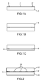
- the Figure 1A represents a plate 2 which comprises, on its front face 4, alignment areas 6, 6 '. These zones, including marks or alignment marks, will make it possible to dispose of the components and / or any other semiconductor element, for example another wafer, in a certain position by relative to the surface 4 of the substrate 2.
- This plate 2 is carried by its front face on a plate 8 handle ( Figure 1B ). But the latter then masks the alignment marks or marks 6, 6 'and prevents the desired alignment from being achieved.
- the figure 1C represents the same wafer 2, after a thinning operation, the marks are still not visible.
- FIG. 2 Another case that may arise is that illustrated in figure 2 where a cover 12 is carried on the front face of a wafer 10 having sensitive areas 14 to protect (for example having a MEMS, or NEMS, or MOEMS etc ).
- the figure 3A is precisely the assembly of a transparent handle 16 with a plate 18, at high temperature.
- the term "functional plate” means any microelectronic structure, for example a “wafer”, comprising components of michronic dimensions.
- the term "viewing window” is understood to mean any element made of a material transparent to the wavelength used, most often in the visible range, for visualizing the marks in the alignment areas. This material may be, for example, air, or a liquid, or a solid.
- the alignment areas may include one or more alignment marks.
- the section of the cavities, in a plane of the wafer, may be arbitrary: a cavity may have a circular or polygonal section.
- This section may have a surface that may be between, for example, a few square millimeters and a few square centimeters, for example between 5 mm 2 and 10 cm 2 .
- Each cavity has an opening, in a first face of the handle plate, through which the material of the transparent window is introduced, while the bottom of the cavity is either closed, and preferably plane, or rests on a surface, preferably plane, aligned with a second face of the handle plate, substantially parallel to the first face. There is therefore an alignment surface that positions the window or its material in each cavity.
- a through cavity is formed, and, before step b), said handle plate is assembled with a support substrate, which can be removed after the step b).
- This support then provides the alignment or reception surface or a surface parallel to this alignment or reception surface.
- the wafer and the support substrate can be assembled using a reversible adhesive bond, in which case it is the bonding layer adhesive that forms the alignment or reception surface.
- the support substrate can be removed after step b) by shearing the handle plate and the support substrate.
- an adhesive bond of the thermofusible polymer type is advantageously used.
- step a it is possible, during step a), a non-through cavity. It is the bottom of the cavity that then forms the alignment or reception surface. In this case, it is possible, after step b), to eliminate a part of the thickness of the wafer so that the at least one cavity passes through the thinned wafer.
- step b) it is possible to insert in said cavity a transparent or visual liquid material, which is then solidified.
- step b) at least one transparent or viewing window made of a solid material is inserted into said cavity, over all or part of its depth.
- the invention also relates to a handle plate for a microelectronic substrate or a microelectronic functional wafer, comprising at least one cavity and / or a transparent or viewing window through the thickness of the wafer handle.
- the invention also relates to a method for treating or handling a wafer, or functional wafer, comprising at least one marking or alignment zone, comprising an assembly of this wafer with a wafer handle according to the invention or obtained by a method according to the invention, so that a window of the handle makes it possible to display all or part of at least one alignment mark through the handle, and possibly the treatment of said functional wafer or wafer.
- This treatment may comprise, for example, at least one thinning and / or in an assembly with another substrate.
- the wafer handle can be removed or preserved. If it is maintained, then it plays the role of a hood.
- the wafer may further comprise at least one component, for example of MEMS or NEMS or MOEMS type.
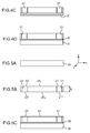
- FIG. 4A-4D A first example of the use of a handle 20 'according to the invention is represented in Figures 4A-4D .
- a plate 2 comprises, on its front face 4, alignment marks 6, 6 ', such as that of the Figure 1A .
- This plate is linked by its front face with a plate 20, also called plate handle ( Figure 4A ), but the latter is provided with windows 22, 24, which allow access to a vision of the alignment sights 6, 6 '.
- the Figure 4B represents a variant in which the substrate is of the type presented above with the figure 2 and whose surface incorporates not only alignment marks 6, 6 ', but also components 14, for example MEMS, NEMS, MOEMS etc ).
- This plate is bound by its front face with a plate 20 'handle, also provided with windows 22, 24, which provide access to a vision of the alignment patterns 6, 6'.
- the wafer 2 can then be thinned, then treated on the rear face 2 ', to form the structure of the figure 4C .
- the same result can be obtained with the plate 10 of the Figure 4B .
- Other treatments of the wafer 2 may be carried out, alternatively or in combination with a thinning, for example an assembly with another substrate such as the substrate 100 of the Figure 4B .
- a handle device for example of silicon or of another semiconductor material such as AsGa, or a ceramic or a polymer ( Figures 5A , 6A , 7A ).
- the wafer in which the windows will be integrated has a coefficient of thermal expansion (CTE) equivalent to, or close to, that of the wafer to be treated (or functional wafer), which will then be reported on the wafer provided with the windows.
- CTE coefficient of thermal expansion
- the wafer to be treated is of semiconductor material, for example silicon.
- the wafer which will make it possible to form the wafer handle has an extension in an xy plane.
- Its thickness E, measured in a direction z perpendicular to the xy plane, is small, for example between a few hundred micrometers and a few millimeters, for example still between 100 microns and 1 mm or 5 mm.
- Cavities 21, 23, 41, 43, 61, 63 are etched in this plate 20 (FIG. Figures 5B , 6B, 7B ).
- these etching mention may be made of techniques by laser, or by ultrasonic machining, or by sandblasting, or by plasma, or a chemical technique (in particular: etching with KOH, with TMAH, or with Xenon fluoride).
- the windows may be for example of a solid or solidified material, for example borosilicate glass or soda-lime glass or fusible glass or fused silica or silicone or epoxy.
- cavities 21, 23 are etched into the handle plate 20 (FIG. Figure 5B ).
- the resulting cavities 21, 23 obtained here are through, they therefore have a thickness identical to that E of the wafer itself.
- This plate with its cavities, is transferred temporarily to a flat-surface support 30 provided with a layer of adhesive 32 ( Figure 5C ).
- a layer of adhesive 32 ( Figure 5C ).
- This the latter is for example of the hot melt type, the adhesion can be removed by heating.
- Each cavity initially comprises an opening 21 ', 23', in a first main face 20 1 of the handle plate 20, through which the material of the transparent window will then be introduced.
- the second opening 21 ", 23" of each cavity is closed.
- the bottom of the cavity rests on a plane surface aligned with a second face 2 of the handle plate 20, substantially parallel to the first face 20 1 .
- a transparent window 31, 33 for example glass, quartz or polymer
- the sealing material is designated on the figure 5E by the references 31 ', 33'.
- the plate 20 'with its windows 31, 33 can then be transferred to another plate 40 by known technologies, for example of the "wafer bonding" type, using a resin 35, a type of fuse material eutectic or by anodic sealing ( figure 5G ).
- This wafer 40 may be of the type of the wafer 2 or the wafer 10 described above, respectively in connection with the Figures 1A and 2 , and have patterns or alignment marks as already explained. These marks or marks, positioned on the front face, can be seen through the windows of the handle and thus be used to allow alignment of the rear face.
- FIG. 6A-6D Another embodiment is shown in Figures 6A-6D .
- cavities 41, 43 are made in this plate by etching. Unlike the embodiment described above, the cavities 41, 43 obtained here are not through, they have a depth e less than the thickness E of the wafer itself.
- cavities are then filled with a transparent material 51, 53, but this time in a liquid or pasty state, while the windows 31, 33 of the previous example were introduced into the cavities 21, 23 while being in the solid state.
- a transparent material 51, 53 for example, fusible glass or fused silica or a polymerizable polymer, for example UV or thermal, may be chosen. This material is then solidified under temperature conditions permitting it.
- Each cavity has an opening 41 ', 43' in the first main face 20 1 of the handle plate 20, through which the material of the transparent window is introduced.
- the non-etched bottom 41 ", 43" of each cavity 41, 43 defines a planar surface for correctly positioning the material of each window in the corresponding cavity, in a plane parallel to the xy plane of the wafer 20 and in the vertical direction z, perpendicular to the xy plane of the wafer 20.
- the wafer can then be thinned, at least at the bottom 41 ", 42" of each cavity, in order to show, on each of the two main faces 20 1 , 20 2 of the wafer, the transparent window thus produced, the transparent material is now solid. This eliminates the difference in thickness between the wafer 20 and the cavities 41, 43. In addition, polishing of the front and rear faces of the thinned wafer is also performed, in order to obtain an optical quality.
- This embodiment does not require the implementation of a booster pad (or support), as the wafer 30 of the previous embodiment.
- the alignment of the windows in the second plane of the handle is advantageously achieved through the bottom 41 ", 43" of each cavity. This embodiment makes it possible in particular to use an initially liquid material.
- cavities 61, 63 are etched in this plate ( Figure 7B ). Unlike the embodiment described above, the cavities obtained 61, 63 are here again through, they have a depth e equal to the thickness E of the wafer itself.
- This plate is transferred, provided with its cavities, temporarily on a support 30 with an adhesive 32 '( Figure 7C ) to form a flat alignment or reception surface.
- the adhesive is for example of the hot melt type, the adhesion can be removed by heating, for example of the type developed by Breewer Science for temporary wafer bonding.
- this support 30 and / or its adhesive 32 ' for the alignment or the positioning of the windows, along the axis z perpendicular to the substrate, is the same as in the case of the embodiment explained above in connection with with the Figures 5A - 5G .
- a transparent material 71, 73 in the liquid state for example a transparent polymer of the epoxy or silicone type. This material is then solidified, under temperature conditions permitting.
- the windows may be large enough to be visible by any type of alignment equipment or dedicated to a particular application or equipment.
- a window has a width, or maximum dimension, measured along a direction parallel to the surface of the substrate 20, of the order of a few tens of ⁇ m to a few hundred ⁇ m or a few mm, for example between 100 ⁇ m and 3 ⁇ m. mm or 5 mm.
- the windows of a handle substrate according to the invention have polished faces so as not to lose in resolution.
- a window for viewing a handle substrate according to the invention preferably has a transparency to a radiation in an observation spectral range, which comprises at least part of the visible spectrum (most photolithography equipment includes sensitive cameras in the visible range) or for example between 400 nm or 450 nm or 500 nm on the one hand and 600 nm or 700 nm or 750 nm on the other hand.
- the transparent material of the window may be for example a glass or a polymer.
- the invention furthermore relates to equipment, in particular for photolithography, comprising at least one substrate as described above, with a sensitive camera in at least one spectral range, for example at least one one of those just mentioned, wherein at least one window of the substrate is at least partly transparent.
Landscapes
- Engineering & Computer Science (AREA)
- Physics & Mathematics (AREA)
- Condensed Matter Physics & Semiconductors (AREA)
- General Physics & Mathematics (AREA)
- Computer Hardware Design (AREA)
- Microelectronics & Electronic Packaging (AREA)
- Power Engineering (AREA)
- Manufacturing & Machinery (AREA)
- Micromachines (AREA)
- Container, Conveyance, Adherence, Positioning, Of Wafer (AREA)
- Surface Acoustic Wave Elements And Circuit Networks Thereof (AREA)
Abstract
Description
- L'invention se rapporte aux procédés microélectroniques ou mettant en oeuvre des microsystèmes.
- Dans de tels procédés on peut avoir à réaliser un alignement sur des motifs qui sont eux-mêmes masqués par exemple par un support temporaire (dit poignée) ou par un capot.
- Ce cas se présente par exemple lorsqu'on utilise une plaquette de matériau semi-conducteur amincie, d'épaisseur inférieure à 300µm. Une telle plaquette est alors très fragiles et il n'est pas possible de la manipuler dans des équipements conventionnels de microélectronique.
- Un exemple typique de procédé nécessitant un alignement est la photolithographie. L'alignement avec le masque de photolithographie est réalisé avec des motifs gravés sur la plaquette semi-conductrice. Là encore, un support temporaire (ou poignée) masque ces marques d'alignement.
- La
figure 1A représente une plaquette 2 qui comporte, sur sa face avant 4, des zones d'alignement 6, 6'. Ces zones, comportant des marques ou mires d'alignement, vont permettre de disposer des composants et/ou tout autre élément semi-conducteur, par exemple une autre plaquette, dans une certaine position par rapport à la surface 4 du substrat 2. Cette plaquette 2 est reportée par sa face avant sur une plaquette 8 poignée (figure 1B ). Mais cette dernière masque alors les marques ou mires d'alignement 6, 6' et empêche de réaliser l'alignement souhaité. Lafigure 1C représente la même plaquette 2, après une opération d'amincissement, les marques ne sont toujours pas visibles. - Un autre cas qui peut se présenter est celui illustré en
figure 2 où un capot 12 est reporté sur la face avant d'une plaquette 10 comportant des zones sensibles 14 à protéger (par exemple comportant un MEMS, ou un NEMS, ou un MOEMS etc...) . - Dans ce cas, comme dans le précédent, les zones d'alignement 6, 6' se retrouvent masquées par le capot 12 et ne sont plus visibles.
- A ce jour, les solutions apportées proposent d'utiliser une plaquette poignée 8 transparente ou un capot 12 transparent.
- Cependant lorsque des plaquettes de natures différentes sont assemblées à des températures élevées, la différence d'expansion thermique les deux plaquettes conduit à une déformation de l'ensemble lors d'un retour à la température ambiante. C'est le cas avec des plaquettes en matériau transparent.
- La
figure 3A représente justement l'assemblage d'une poignée transparente 16 avec une plaquette 18, à température élevée. - La situation, après retour à température ambiante, est représentée en
figure 3B , sur laquelle une déformation apparaît. - Cette déformation induit des problèmes de manipulation dans des équipements de microélectronique. Par ailleurs elle dégrade la résolution des motifs obtenus par photolithographie.
- Il se pose donc le problème de trouver une autre technique, qui permet d'éviter l'utilisation d'une poignée en un matériau présentant un coefficient de dilatation thermique trop différent de celui du substrat auquel il est appliqué.
- L'invention concerne d'abord un procédé de réalisation d'une plaquette poignée pour un substrat ou composant microélectronique, ou une plaquette fonctionnelle microélectronique, comportant au moins une fenêtre de visualisation à travers l'épaisseur de la plaquette poignée, ce procédé comportant .
- a) la réalisation d'au moins une cavité dans ladite plaquette poignée,
- b) la formation d'au moins une fenêtre de visualisation dans ladite cavité, sur une surface d'alignement ou d'accueil ou en regard d'une telle surface.
- On entend par « plaquette fonctionnelle » toute structure de micro-électronique, par exemple un «wafer», comportant des composants de dimensions michroniques.
- En outre, on comprend par « fenêtre de visualisation », tout élément en un matériau transparent à la longueur d'onde utilisée, le plus souvent dans le domaine visible, pour visualiser les marques dans les zones d'alignement. Ce matériau peut être par exemple de l'air, ou un liquide, ou encore un solide. Enfin, les zones d'alignement peuvent comporter une ou plusieurs marques d'alignement.
- La section des cavités, dans un plan de la plaquette, peut-être quelconque : une cavité peut avoir une section circulaire ou polygonale.
- Cette section peut avoir une surface qui peut être comprise entre par exemple quelques millimètres carrés et quelques centimètres carrés, par exemple comprise entre 5 mm2 et 10 cm2.
- Chaque cavité comporte une ouverture, dans une première face de la plaquette poignée, par laquelle le matériau de la fenêtre transparente est introduit, tandis que le fond de la cavité est soit fermé, et de préférence plan, soit repose sur une surface, de préférence plane, alignée avec une deuxième face de la plaquette poignée, sensiblement parallèle à la première face. Il y a donc une surface d'alignement qui permet de positionner la fenêtre ou son matériau dans chaque cavité.
- Selon un mode de réalisation, on forme, lors de l'étape a), une cavité traversante, et, avant l'étape b), on assemble ladite plaquette poignée avec un substrat support, que l'on peut retirer après l'étape b). Ce support fournit alors la surface d'alignement ou d'accueil ou une surface parallèle à cette surface d'alignement ou d'accueil.
- La plaquette et le substrat support peuvent être assemblés à l'aide d'une liaison adhésive réversible, auquel cas c'est la couche de liaison adhésive qui forme la surface d'alignement ou d'accueil.
- On peut retirer le substrat support après l'étape b), par un mouvement de cisaillement de la plaquette poignée et du substrat support. A cette fin, on utilise avantageusement une liaison adhésive de type polymère thermofusible.
- En variante, on peut réaliser, lors de l'étape a), une cavité non traversante. C'est le fond de la cavité qui forme alors la surface d'alignement ou d'accueil. Dans ce cas, on peut, après l'étape b), éliminer une partie de l'épaisseur de la plaquette afin que ladite au moins une cavité soit traversante dans la plaquette amincie.
- Lors de l'étape b), on peut insérer dans ladite cavité un matériau liquide transparent ou de visualisation, qui est ensuite solidifié.
- En variante, lors de l'étape b), on insère dans ladite cavité, sur tout ou partie de sa profondeur, au moins une fenêtre transparente ou de visualisation en un matériau solide.
- L'invention concerne également une plaquette poignée pour un substrat microélectronique ou une plaquette fonctionnelle microélectronique, comportant au moins une cavité et/ou une fenêtre transparente ou de visualisation à travers l'épaisseur de la plaquette poignée.
- Dans un procédé ou un dispositif selon l'invention :
- la ou les fenêtre(s) peuvent être en verre borosilicaté ou en verre sodocalcique ou en verre fusible ou en silice fondue ou en silicone ou en polymère,
- et/ou la plaquette peut être en matériau semi-conducteur, ou en matériau céramique ou polymère.
- L'invention concerne également un procédé de traitement ou de manipulation d'une plaquette, ou plaquette fonctionnelle, comportant au moins une marque ou zone d'alignement, comportant un assemblage de cette plaquette avec une plaquette poignée selon l'invention ou obtenue par un procédé selon l'invention, de sorte qu'une fenêtre de la poignée permet de visualiser tout ou partie d'au moins une marque d'alignement à travers la poignée, puis éventuellement le traitement de ladite plaquette ou plaquette fonctionnelle. Ce traitement peut comporter par exemple au moins un amincissement et/ou en un assemblage avec un autre substrat. Après traitement de la plaquette fonctionnelle, la plaquette poignée peut être retirée ou conservée. Si elle est maintenue, elle joue alors le rôle d'un capot.
- La plaquette peut comporter en outre au moins un composant, par exemple de type MEMS ou NEMS ou MOEMS.
-
- Les
figures 1A-1C représentent un procédé selon l'art antérieur, - la
figure 2 représente un assemblage d'un capot avec un substrat supportant des MEMS, - les
figures 3A-3B illustrent les problèmes de différences de CTE, - les
figures 4A-4D représentent des assemblages d'un substrat et d'une poignée selon l'invention, - les
figures 5A-5G représentent un premier procédé de réalisation d'une poignée selon l'invention, - les
figures 6A-6D représentent un deuxième procédé de réalisation d'une poignée selon l'invention, - les
figures 7A-7F représentent un troisième procédé de réalisation d'une poignée selon l'invention, - la
figure 8 représente un dispositif poignée selon l'invention, en vue de dessus. - Un premier exemple de l'utilisation d'une poignée 20' selon l'invention est représenté en
figures 4A-4D . - Une plaquette 2 comporte, sur sa face avant 4, des marques d'alignement 6, 6', comme celle de la
figure 1A . Cette plaquette est liée par sa face avant avec une plaquette 20, dite aussi plaquette poignée (figure 4A ), mais cette dernière est munie de fenêtres 22, 24, qui permettent d'avoir accès à une vision des mires d'alignement 6, 6'. - La
figure 4B représente une variante dans laquelle le substrat est du type présenté ci-dessus avec lafigure 2 et dont la surface incorpore non seulement des marques d'alignement 6, 6', mais également des composants 14, par exemple un MEMS, un NEMS, un MOEMS etc...). Cette plaquette est liée par sa face avant avec une plaquette 20' poignée, elle aussi munie de fenêtres 22, 24, qui permettent d'avoir accès à une vision des mires d'alignement 6, 6'. - Dans le cas de la
figure 4A , la plaquette 2 peut alors être amincie, puis traitée en face arrière 2', pour former la structure de lafigure 4C . Le même résultat peut être obtenu avec la plaquette 10 de lafigure 4B . D'autres traitements de la plaquette 2 peuvent être réalisés, en variante ou en combinaison avec un amincissement, par exemple un assemblage avec un autre substrat tel que le substrat 100 de lafigure 4B . - Sur les
figures 4A - 4C , l'espace, entre les fenêtres et les bords des trous 21, 23 réalisés dans la plaquette et dans lesquels des fenêtres, est comblé avec un revêtement 22', 24'. - Dans une variante, exposée en
figure 4D , on s'affranchit d'introduire ou de former une fenêtre, en particulier une fenêtre solide, dans ces trous. - Plusieurs exemples de réalisation d'un dispositif poignée, selon l'invention, vont être décrits. On considère au départ de tous ces exemples une plaquette de départ 20 par exemple en silicium ou en un autre matériau semi-conducteur tel que l'AsGa, ou une céramique ou un polymère (
figures 5A ,6A ,7A ). Ainsi la plaquette dans laquelle seront intégrées les fenêtres a un coefficient de dilatation thermique (CTE) équivalent à, ou proche de, celui de la plaquette à traiter (ou encore plaquette fonctionnelle), qui sera reportée ensuite sur la plaquette munie des fenêtres. En général la plaquette à traiter est en matériau semi-conducteur, par exemple en silicium. - La plaquette qui va permettre de former la plaquette poignée a une extension dans un plan xy. Son épaisseur E, mesurée suivant une direction z perpendiculaire au plan xy, est faible, par exemple comprise entre quelques centaines de micromètres et quelques millimètres, par exemple encore comprise entre 100 µm et 1 mm ou 5 mm.
- On réalise, par gravure, des cavités 21, 23 41, 43, 61, 63 dans cette plaquette 20 (
figures 5B ,6B, 7B ). Parmi les techniques que l'on peut utiliser pour cette gravure, on peut citer les techniques par laser, ou par usinage ultrasonique, ou par sablage, ou par plasma, ou une technique chimique (notamment : gravure au KOH, au TMAH, ou au fluorure de Xénon). - Dans les divers exemples donnés, les fenêtres peuvent être par exemple en un matériau solide ou solidifié, par exemple en verre borosilicaté ou en verre sodocalcique ou en verre fusible ou en silice fondue ou en silicone ou en époxy.
- Le premier exemple va être décrit en liaison avec les
figures 5A-5F . - Comme expliqué ci-dessus, on réalise, par gravure, des cavités 21, 23 dans la plaquette poignée 20 (
figure 5B ). Les cavités obtenues 21, 23 obtenues sont ici traversantes, elles ont donc une épaisseur identique à celle E de la plaquette elle-même. - On reporte cette plaquette, munie de ses cavités, temporairement sur un support 30 à surface plane, munie d'une couche d'adhésif 32 (
figure 5C ). Ce dernier est par exemple de type thermofusible, dont l'adhésion peut être éliminée par chauffage. - Chaque cavité comporte initialement une ouverture 21', 23', dans une première face principale 201 de la plaquette poignée 20, par laquelle le matériau de la fenêtre transparente sera ensuite introduit. Par report sur la plaquette support 30, on ferme la deuxième ouverture 21", 23" de chaque cavité. Ainsi le fond de la cavité repose sur une surface plane alignée avec une deuxième face 202 de la plaquette poignée 20, sensiblement parallèle à la première face 201.
- On peut ensuite positionner ou introduire une fenêtre transparente 31, 33, par exemple en verre, en quartz ou en polymère, dans chaque cavité 21, 23 (
figure 5D ). Le support 30, ou la surface de sa couche d'adhésif opposée à la surface du support 30 sur laquelle cette couche repose, fournit une surface plane d'accueil ou d'alignement pour positionner correctement la fenêtre dans la cavité, dans la direction verticale z, perpendiculaire au plan xy de la plaquette 20. Mais la fenêtre peut ne pas remplir la cavité et en particulier être en retrait par rapport à cette surface d'accueil. - On procède alors à un scellement de ces fenêtres dans ces cavités. Le matériau de scellement est désigné sur la
figure 5E par les références 31',33'. - Il est ensuite possible de retirer le support 30 (
figure 5F ) par élimination de l'adhésif, ce qui libère la deuxième face 202 de la plaquette. Les fenêtres 31, 33 sont alors exposées au niveau de chacune des deux faces 201, 202. - On peut également procéder à un polissage des faces avant et arrière de la plaquette 20' ainsi obtenue pour disposer d'une qualité optique.
- La plaquette 20' avec ses fenêtres 31, 33 peut être ensuite reportée sur une autre plaquette 40 par des technologies connues, par exemple de type "wafer bonding", à l'aide d'une résine 35, d'un matériau fusible de type eutectique ou par scellement anodique (
figure 5G ). Cette plaquette 40 peut être du type de la plaquette 2 ou de la plaquette 10 décrites ci-dessus, respectivement en liaison avec lesfigures 1A et 2 , et comporter des mires ou des marques d'alignement comme déjà expliqué. Ces mires ou marques, positionnées en face avant, pourront être vues à travers les fenêtres de la poignée et ainsi être utilisées pour permettre un alignement de la face arrière. - Un autre exemple de réalisation est représenté en
figures 6A-6D . - Dans la plaquette 20 de départ (
figure 6A ), on réalise, ici encore par gravure, des cavités 41, 43 dans cette plaquette. A la différence du mode de réalisation exposé précédemment, les cavités obtenues 41, 43 ne sont ici pas traversantes, elles ont donc une profondeur e inférieure à l'épaisseur E de la plaquette elle-même. - On procède ensuite au remplissage de ces cavités avec un matériau 51, 53 transparent, mais cette fois à l'état liquide, ou pâteux, alors que les fenêtres 31, 33 de l'exemple précédent étaient introduites dans les cavités 21, 23 en étant à l'état solide. On peut choisir ici, par exemple, le verre fusible ou la silice fondue ou un polymère polymérisable, UV ou thermique par exemple. Ce matériau est ensuite solidifié, dans des conditions de température le permettant.
- Chaque cavité comporte une ouverture 41', 43', dans la première face principale 201 de la plaquette poignée 20, par laquelle le matériau de la fenêtre transparente est introduit. Le fond non gravé 41" , 43" de chaque cavité 41, 43 définit une surface plane pour positionner correctement le matériau de chaque fenêtre dans la cavité correspondante, dans un plan parallèle au plan xy de la plaquette 20 et suivant la direction verticale z, perpendiculaire au plan xy de la plaquette 20.
- On peut procéder ensuite à un amincissement de la plaquette, jusque, au moins, au niveau du fond 41", 42" de chaque cavité, afin de faire apparaître, sur chacune des deux faces principales 201, 202 de la plaquette, la fenêtre transparente ainsi réalisée, le matériau transparent étant maintenant solide. On élimine ainsi la différence d'épaisseur entre la plaquette 20 et les cavités 41, 43. On réalise en outre, éventuellement, un polissage des faces avant et arrière de la plaquette amincie, afin d'obtenir une qualité optique.
- Ce mode de réalisation ne nécessite pas la mise en oeuvre d'une plaquette d'appoint (ou support), comme la plaquette 30 du mode de réalisation précédent. L'alignement des fenêtres dans le deuxième plan de la poignée est avantageusement réalisé grâce au fond 41" , 43" de chaque cavité. Ce mode de réalisation permet en particulier d'utiliser un matériau initialement liquide.
- Un autre exemple de réalisation est représenté en
figures 7A - 7F . - Là encore, partant d'une plaquette de départ 20 on réalise, par gravure, des cavités 61, 63 dans cette plaquette (
figure 7B ). A la différence du mode de réalisation exposé précédemment, les cavités obtenues 61, 63 sont ici de nouveau traversantes, elles ont donc une profondeur e égale à l'épaisseur E de la plaquette elle-même. - On reporte cette plaquette, munie de ses cavités, temporairement sur un support 30 avec un adhésif 32' (
figure 7C ) pour former une surface plane d'alignement ou d'accueil. L'adhésif est par exemple de type thermofusible, dont l'adhésion peut être éliminée par chauffage, par exemple du type de celle développée par Breewer Science pour le collage de plaquette temporaire. - Le rôle de ce support 30 et/ou de son adhésif 32', pour l'alignement ou le positionnement des fenêtres, suivant l'axe z perpendiculaire au substrat, est le même que dans le cas du mode de réalisation expliqué ci dessus en liaison avec les
figures 5A - 5G . - On procède ensuite au remplissage de ces cavités avec un matériau 71, 73 transparent, à l'état liquide (
figure 7D ), par exemple un polymère transparent de type époxy ou silicone. Ce matériau est ensuite solidifié, dans des conditions de température le permettant. - Il est ensuite possible de retirer le support 30 (
figure 7E ), par cisaillement à haute température de la couche 32. - On peut également procéder à un nettoyage et/ou un polissage des faces avant et arrière de la plaquette 20' ainsi obtenue pour disposer d'une qualité optique.
- Quel que soit le mode de réalisation choisi, les fenêtres peuvent être suffisamment larges pour être visibles par tout type d'équipement d'alignement ou bien dédiée à une application ou un équipement particulier. Par exemple une fenêtre a une largeur, ou dimension maximale, mesurée suivant une direction parallèle à la surface du substrat 20, de l'ordre de quelques dizaines de µm à quelques centaines de µm ou quelques mm, par exemple comprise entre 100 µm et 3 mm ou 5 mm.
- Avantageusement les fenêtres d'un substrat poignée selon l'invention ont des faces polies de façon à ne pas perdre en résolution.
- Une fenêtre de visualisation d'un substrat poignée selon l'invention a de préférence une transparence à un rayonnement dans un domaine spectral d'observation, qui comporte au moins une partie du spectre visible (la plupart des équipements de photolithographie comportent des cameras sensibles dans le domaine du visible) ou par exemple entre, d'une part, 400 nm ou 450 nm ou 500 nm et, d'autre part, 600 nm ou 700 nm ou 750 nm. Le matériau transparent de la fenêtre pourra être par exemple un verre ou un polymère. L'invention concerne d'ailleurs en outre un équipement, en particulier pour la photolithographie, comportant au moins un substrat tel qu'il a été décrit ci-dessus, avec une caméra sensible dans au moins un domaine spectral, par exemple au moins l'un de ceux qui viennent d'être énoncés, dans lequel au moins une fenêtre du substrat est au moins en partie transparente.
Claims (15)
- Procédé de réalisation d'une plaquette (20') poignée pour des plaquettes fonctionnelles microélectroniques, comportant au moins une fenêtre (31, 33, 51, 53, 61, 63), en un matériau solide ou solidifié, de visualisation à travers l'épaisseur de la plaquette poignée, ce procédé comportant :a) la réalisation d'au moins une cavité (21, 23, 41, 43, 61, 63) dans ladite plaquette poignée,b) la formation d'au moins une fenêtre de visualisation (31, 33, 51, 53, 71, 73) dans ladite cavité, sur une surface d'alignement ou d'accueil (32, 41" , 43" , 32').
- Procédé selon la revendication 1, dans lequel on réalise, lors de l'étape a), une cavité traversante (21, 23, 63), et, avant l'étape b), on assemble ladite plaquette poignée avec un substrat support (30), définissant ladite surface d'alignement ou d'accueil ou une surface parallèle à ladite surface d'alignement ou d'accueil.
- Procédé selon la revendication 2, dans lequel on retire le substrat support (30) après l'étape b) .
- Procédé selon la revendication 2 ou 3, dans lequel ladite plaquette poignée et le substrat support (30) sont assemblés à l'aide d'une liaison adhésive réversible (32, 32') définissant ladite surface d'alignement ou d'accueil.
- Procédé selon la revendication 4, dans lequel on retire le substrat support (30) après l'étape b), par un mouvement de cisaillement de la plaquette poignée et du substrat support.
- Procédé selon la revendication 1, dans lequel on réalise, lors de l'étape a), une cavité non traversante (41, 43), dont le fond (41", 43") plan définit ladite surface d'accueil, et, après l'étape b), on élimine une partie de l'épaisseur de la plaquette afin que ladite au moins cavité soit traversante dans la plaquette amincie (20').
- Procédé selon l'une des revendications 1 à 6, dans lequel, lors de l'étape b), on insère dans ladite cavité un matériau liquide de visualisation (51, 53, 71, 73), qui est ensuite solidifié.
- Procédé selon l'une des revendications 1 à 7, dans lequel, lors de l'étape b), on insère dans tout ou partie de ladite cavité au moins une fenêtre de visualisation (31, 33) en un matériau solide.
- Plaquette (20') poignée pour des plaquettes fonctionnelles microélectroniques, comportant au moins cavité à travers l'épaisseur de la plaquette, cette cavité comportant une fenêtre de visualisation, en un matériau solide ou solidifié.
- Plaquette selon la revendication 9, dans laquelle la ou les fenêtre(s) est, ou sont, en en verre borosilicaté ou en verre sodocalcique ou en verre fusible ou en silice fondue ou en silicone ou en polymère.
- Plaquette selon la revendication 9 ou 10, la plaquette étant en matériau semi-conducteur, ou en matériau céramique ou polymère.
- Procédé de traitement d'une plaquette (2) fonctionnelle comportant au moins une zone d'alignement (6, 6'), comportant un assemblage de cette plaquette avec une plaquette poignée (20') selon l'une des revendications 9 à 11, de sorte qu'une fenêtre permet de visualiser tout ou partie d'au moins une zone d'alignement à travers ladite poignée, puis le traitement de ladite plaquette fonctionnelle.
- Procédé selon la revendication 12, la plaquette fonctionnelle (2) comportant en outre au moins un composant (14).
- Procédé selon la revendication 13, ledit composant (14) étant un MEMS ou un NEMS ou un MOEMS.
- Procédé selon l'une des revendications 12 à 14, ladite plaquette poignée étant éliminée après traitement de ladite plaquette fonctionnelle.
Applications Claiming Priority (1)
| Application Number | Priority Date | Filing Date | Title |
|---|---|---|---|
| FR0954779A FR2947948B1 (fr) | 2009-07-09 | 2009-07-09 | Plaquette poignee presentant des fenetres de visualisation |
Publications (3)
| Publication Number | Publication Date |
|---|---|
| EP2273548A2 true EP2273548A2 (fr) | 2011-01-12 |
| EP2273548A3 EP2273548A3 (fr) | 2014-04-30 |
| EP2273548B1 EP2273548B1 (fr) | 2018-10-17 |
Family
ID=41395925
Family Applications (1)
| Application Number | Title | Priority Date | Filing Date |
|---|---|---|---|
| EP10168442.1A Not-in-force EP2273548B1 (fr) | 2009-07-09 | 2010-07-05 | Procédé de réalisation d'une plaquette poignée presentant des fenêtres de visualisation |
Country Status (4)
| Country | Link |
|---|---|
| US (1) | US8288841B2 (fr) |
| EP (1) | EP2273548B1 (fr) |
| JP (1) | JP2011018907A (fr) |
| FR (1) | FR2947948B1 (fr) |
Families Citing this family (5)
| Publication number | Priority date | Publication date | Assignee | Title |
|---|---|---|---|---|
| CN103824787B (zh) * | 2012-11-16 | 2016-09-07 | 中国科学院上海微系统与信息技术研究所 | 基于粘接剂的晶圆键合方法 |
| US9385089B2 (en) * | 2013-01-30 | 2016-07-05 | Seagate Technology Llc | Alignment mark recovery with reduced topography |
| US9343089B2 (en) | 2013-03-08 | 2016-05-17 | Seagate Technology Llc | Nanoimprint lithography for thin film heads |
| FR3030880B1 (fr) * | 2014-12-19 | 2018-05-11 | Commissariat Energie Atomique | Procede de transformation d'un dispositif electronique |
| CN111081629B (zh) * | 2019-11-04 | 2022-08-16 | 宁波华彰企业管理合伙企业(有限合伙) | 带空腔soi晶圆的对准标记制作方法和空腔位置确定方法 |
Family Cites Families (38)
| Publication number | Priority date | Publication date | Assignee | Title |
|---|---|---|---|---|
| US4322980A (en) * | 1979-11-08 | 1982-04-06 | Hitachi, Ltd. | Semiconductor pressure sensor having plural pressure sensitive diaphragms and method |
| ES8700500A1 (es) | 1984-02-17 | 1986-11-16 | American Telephone & Telegraph | Perfeccionamientos en dispositivos de circuitos integrados |
| US6379998B1 (en) * | 1986-03-12 | 2002-04-30 | Hitachi, Ltd. | Semiconductor device and method for fabricating the same |
| US4958216A (en) * | 1987-03-23 | 1990-09-18 | Kyocera Corporation | Package for housing semiconductor elements |
| GB2202673B (en) | 1987-03-26 | 1990-11-14 | Haroon Ahmed | The semi-conductor fabrication |
| GB2224600B (en) | 1988-10-29 | 1992-03-18 | Stc Plc | Circuit assembly |
| US5353498A (en) * | 1993-02-08 | 1994-10-11 | General Electric Company | Method for fabricating an integrated circuit module |
| US5353195A (en) * | 1993-07-09 | 1994-10-04 | General Electric Company | Integral power and ground structure for multi-chip modules |
| US5904502A (en) * | 1997-09-04 | 1999-05-18 | International Business Machines Corporation | Multiple 3-dimensional semiconductor device processing method and apparatus |
| SE515032C2 (sv) | 1998-09-09 | 2001-06-05 | Ericsson Telefon Ab L M | Elektronikanordning innefattande en komponentbärare samt dylik komponentbärare och en metod för framställning av anordningen |
| DE19907295C1 (de) | 1999-02-22 | 2001-02-08 | Univ Dresden Tech | Verfahren zur Montage elektronischer und/oder optischer Bauelemente und Baugruppen auf der Rückseite einseitig bestückter flexibler Leiterplatten |
| US6982478B2 (en) * | 1999-03-26 | 2006-01-03 | Oki Electric Industry Co., Ltd. | Semiconductor device and method of fabricating the same |
| US6154366A (en) * | 1999-11-23 | 2000-11-28 | Intel Corporation | Structures and processes for fabricating moisture resistant chip-on-flex packages |
| US6875671B2 (en) * | 2001-09-12 | 2005-04-05 | Reveo, Inc. | Method of fabricating vertical integrated circuits |
| EP1500141A1 (fr) * | 2002-04-11 | 2005-01-26 | Koninklijke Philips Electronics N.V. | Dispositif electronique et procede de fabrication correspondant |
| US6998328B2 (en) | 2002-11-06 | 2006-02-14 | Irvine Sensors Corp. | Method for creating neo-wafers from singulated integrated circuit die and a device made according to the method |
| AU2003221149A1 (en) * | 2003-03-25 | 2004-10-18 | Fujitsu Limited | Method for manufacturing electronic component-mounted board |
| WO2004112136A1 (fr) | 2003-06-12 | 2004-12-23 | Koninklijke Philips Electronics N.V. | Dispositif electronique |
| FR2857157B1 (fr) * | 2003-07-01 | 2005-09-23 | 3D Plus Sa | Procede d'interconnexion de composants actif et passif et composant heterogene a faible epaisseur en resultant |
| TWI272654B (en) * | 2003-07-18 | 2007-02-01 | Asia Pacific Microsystems Inc | Method for keeping the precision of photolithography alignment after wafer bonding |
| DE10334576B4 (de) * | 2003-07-28 | 2007-04-05 | Infineon Technologies Ag | Verfahren zum Herstellen eines Halbleiterbauelements mit einem Kunststoffgehäuse |
| FR2864342B1 (fr) | 2003-12-19 | 2006-03-03 | 3D Plus Sa | Procede d'interconnexion de composants electroniques sans apport de brasure et dispositif electronique obtenu par un tel procede |
| DE102004010956B9 (de) * | 2004-03-03 | 2010-08-05 | Infineon Technologies Ag | Halbleiterbauteil mit einem dünnen Halbleiterchip und einem steifen Verdrahtungssubstrat sowie Verfahren zur Herstellung und Weiterverarbeitung von dünnen Halbleiterchips |
| JP4381860B2 (ja) * | 2004-03-24 | 2009-12-09 | 日東電工株式会社 | 補強半導体ウエハに固定された補強板の分離方法およびその装置 |
| US7406761B2 (en) * | 2005-03-21 | 2008-08-05 | Honeywell International Inc. | Method of manufacturing vibrating micromechanical structures |
| TWI271807B (en) * | 2005-03-29 | 2007-01-21 | Phoenix Prec Technology Corp | Chip embedded package structure and fabrication method thereof |
| JP4577688B2 (ja) * | 2005-05-09 | 2010-11-10 | エルピーダメモリ株式会社 | 半導体チップ選択方法、半導体チップ及び半導体集積回路装置 |
| DE102005024431B4 (de) * | 2005-05-24 | 2009-08-06 | Infineon Technologies Ag | Verfahren zur Herstellung von Halbleiterbauteilen unter Verwendung einer Trägerplatte mit doppelseitig klebender Klebstofffolie |
| US7768113B2 (en) * | 2005-05-26 | 2010-08-03 | Volkan Ozguz | Stackable tier structure comprising prefabricated high density feedthrough |
| US20070004171A1 (en) * | 2005-06-30 | 2007-01-04 | Arana Leonel R | Method of supporting microelectronic wafer during backside processing using carrier having radiation absorbing film thereon |
| US20070080458A1 (en) * | 2005-10-11 | 2007-04-12 | Tsuyoshi Ogawa | Hybrid module and method of manufacturing the same |
| JP5164362B2 (ja) * | 2005-11-02 | 2013-03-21 | キヤノン株式会社 | 半導体内臓基板およびその製造方法 |
| JP2007206399A (ja) * | 2006-02-02 | 2007-08-16 | Tokai Rika Co Ltd | 照光表示体及び照光表示体の製造方法 |
| US20080142946A1 (en) * | 2006-12-13 | 2008-06-19 | Advanced Chip Engineering Technology Inc. | Wafer level package with good cte performance |
| FR2917234B1 (fr) * | 2007-06-07 | 2009-11-06 | Commissariat Energie Atomique | Dispositif multi composants integres dans une matrice semi-conductrice. |
| US8338267B2 (en) * | 2007-07-11 | 2012-12-25 | Sematech, Inc. | Systems and methods for vertically integrating semiconductor devices |
| KR100926652B1 (ko) * | 2007-11-08 | 2009-11-16 | 세크론 주식회사 | 웨이퍼 정렬 방법 및 플립칩 제조 방법 |
| FR2934082B1 (fr) * | 2008-07-21 | 2011-05-27 | Commissariat Energie Atomique | Dispositif multi composants integres dans une matrice |
-
2009
- 2009-07-09 FR FR0954779A patent/FR2947948B1/fr not_active Expired - Fee Related
-
2010
- 2010-06-30 US US12/827,171 patent/US8288841B2/en active Active
- 2010-07-05 EP EP10168442.1A patent/EP2273548B1/fr not_active Not-in-force
- 2010-07-08 JP JP2010155684A patent/JP2011018907A/ja active Pending
Non-Patent Citations (1)
| Title |
|---|
| None |
Also Published As
| Publication number | Publication date |
|---|---|
| EP2273548A3 (fr) | 2014-04-30 |
| FR2947948A1 (fr) | 2011-01-14 |
| FR2947948B1 (fr) | 2012-03-09 |
| EP2273548B1 (fr) | 2018-10-17 |
| US8288841B2 (en) | 2012-10-16 |
| US20110006400A1 (en) | 2011-01-13 |
| JP2011018907A (ja) | 2011-01-27 |
Similar Documents
| Publication | Publication Date | Title |
|---|---|---|
| EP2273548B1 (fr) | Procédé de réalisation d'une plaquette poignée presentant des fenêtres de visualisation | |
| EP2162907B1 (fr) | Dispositif comportant des composants encastrés dans des cavités d'une plaquette d'accueil et procédé correspondant | |
| EP1634685A2 (fr) | Puce mince en verre pour composant électronique et procédé de fabrication | |
| FR2797347A1 (fr) | Procede de transfert d'une couche mince comportant une etape de surfragililisation | |
| EP1815509A2 (fr) | Amincissement d'une plaquette semiconductrice | |
| US8981500B2 (en) | Method for producing an optical window device for a MEMS device | |
| CA2587431C (fr) | Procede de fabrication collective de microstructures a elements superposes | |
| JP2005528782A (ja) | 基板およびコンポジット要素の接続方法 | |
| US10752500B2 (en) | Method for producing optical components using functional elements | |
| Stanković et al. | Die-to-die adhesive bonding procedure for evanescently-coupled photonic devices | |
| EP1364400B9 (fr) | Procede de fabrication de couches minces sur un support specifique et une application | |
| WO2006043000A2 (fr) | Procede de transfert d'au moins un objet de taille micrometrique ou millimetrique au moyen d'une poignee en polymere | |
| TW200910435A (en) | Method of wafer-level segmenting capable of protecting contact pad | |
| EP2829511A2 (fr) | Dispositif comportant un canal fluidique muni d'au moins un systeme micro ou nanoélectronique et procédé de réalisation d'un tel dispositif | |
| FR2944646A1 (fr) | Procede de realisation d'une cavite dans l'epaisseur d'un substrat pouvant former un site d'accueil de composant | |
| EP3497711B1 (fr) | Procédé de fabrication d'une couche épitaxiée sur une plaque de croissance | |
| EP2798667B1 (fr) | Procede de fabrication d'une structure multicouche sur un support | |
| EP3035378B1 (fr) | Procédé de transformation d'un dispositif électronique utilisable dans un procédé de collage temporaire d'une plaque sur une poignée et dispositif électronique fabriqué par le procédé | |
| EP2456625B1 (fr) | Procede de realisation d'un dispositif a element graphique | |
| US20230377935A1 (en) | Temporary bonding method | |
| FR3105570A1 (fr) | Poignee pour puces destinees a etre collees par collage direct a un substrat recepteur | |
| JP2018526232A (ja) | マイクロメカニカル窓構造の製造方法およびそれに対応するマイクロメカニカル窓構造 | |
| FR2966452A1 (fr) | Procédé de réalisation d'une structure a canal microfluidique, composants et structure a canal microfluidique |
Legal Events
| Date | Code | Title | Description |
|---|---|---|---|
| PUAI | Public reference made under article 153(3) epc to a published international application that has entered the european phase |
Free format text: ORIGINAL CODE: 0009012 |
|
| AK | Designated contracting states |
Kind code of ref document: A2 Designated state(s): AL AT BE BG CH CY CZ DE DK EE ES FI FR GB GR HR HU IE IS IT LI LT LU LV MC MK MT NL NO PL PT RO SE SI SK SM TR |
|
| AX | Request for extension of the european patent |
Extension state: BA ME RS |
|
| PUAL | Search report despatched |
Free format text: ORIGINAL CODE: 0009013 |
|
| AK | Designated contracting states |
Kind code of ref document: A3 Designated state(s): AL AT BE BG CH CY CZ DE DK EE ES FI FR GB GR HR HU IE IS IT LI LT LU LV MC MK MT NL NO PL PT RO SE SI SK SM TR |
|
| AX | Request for extension of the european patent |
Extension state: BA ME RS |
|
| RIC1 | Information provided on ipc code assigned before grant |
Ipc: H01L 23/544 20060101AFI20140321BHEP Ipc: H01L 21/68 20060101ALI20140321BHEP Ipc: B81C 3/00 20060101ALI20140321BHEP Ipc: H01L 21/683 20060101ALI20140321BHEP |
|
| 17P | Request for examination filed |
Effective date: 20141029 |
|
| RBV | Designated contracting states (corrected) |
Designated state(s): AL AT BE BG CH CY CZ DE DK EE ES FI FR GB GR HR HU IE IS IT LI LT LU LV MC MK MT NL NO PL PT RO SE SI SK SM TR |
|
| STAA | Information on the status of an ep patent application or granted ep patent |
Free format text: STATUS: EXAMINATION IS IN PROGRESS |
|
| 17Q | First examination report despatched |
Effective date: 20170518 |
|
| GRAP | Despatch of communication of intention to grant a patent |
Free format text: ORIGINAL CODE: EPIDOSNIGR1 |
|
| STAA | Information on the status of an ep patent application or granted ep patent |
Free format text: STATUS: GRANT OF PATENT IS INTENDED |
|
| INTG | Intention to grant announced |
Effective date: 20180511 |
|
| RIN1 | Information on inventor provided before grant (corrected) |
Inventor name: SOURIAU, JEAN-CHARLES Inventor name: CAPLET, STEPHANE |
|
| GRAS | Grant fee paid |
Free format text: ORIGINAL CODE: EPIDOSNIGR3 |
|
| GRAA | (expected) grant |
Free format text: ORIGINAL CODE: 0009210 |
|
| STAA | Information on the status of an ep patent application or granted ep patent |
Free format text: STATUS: THE PATENT HAS BEEN GRANTED |
|
| AK | Designated contracting states |
Kind code of ref document: B1 Designated state(s): AL AT BE BG CH CY CZ DE DK EE ES FI FR GB GR HR HU IE IS IT LI LT LU LV MC MK MT NL NO PL PT RO SE SI SK SM TR |
|
| REG | Reference to a national code |
Ref country code: GB Ref legal event code: FG4D Free format text: NOT ENGLISH |
|
| REG | Reference to a national code |
Ref country code: CH Ref legal event code: EP |
|
| REG | Reference to a national code |
Ref country code: IE Ref legal event code: FG4D Free format text: LANGUAGE OF EP DOCUMENT: FRENCH |
|
| REG | Reference to a national code |
Ref country code: DE Ref legal event code: R096 Ref document number: 602010054354 Country of ref document: DE Ref country code: AT Ref legal event code: REF Ref document number: 1054979 Country of ref document: AT Kind code of ref document: T Effective date: 20181115 |
|
| REG | Reference to a national code |
Ref country code: NL Ref legal event code: MP Effective date: 20181017 |
|
| REG | Reference to a national code |
Ref country code: LT Ref legal event code: MG4D |
|
| REG | Reference to a national code |
Ref country code: AT Ref legal event code: MK05 Ref document number: 1054979 Country of ref document: AT Kind code of ref document: T Effective date: 20181017 |
|
| PG25 | Lapsed in a contracting state [announced via postgrant information from national office to epo] |
Ref country code: NL Free format text: LAPSE BECAUSE OF FAILURE TO SUBMIT A TRANSLATION OF THE DESCRIPTION OR TO PAY THE FEE WITHIN THE PRESCRIBED TIME-LIMIT Effective date: 20181017 |
|
| PG25 | Lapsed in a contracting state [announced via postgrant information from national office to epo] |
Ref country code: IS Free format text: LAPSE BECAUSE OF FAILURE TO SUBMIT A TRANSLATION OF THE DESCRIPTION OR TO PAY THE FEE WITHIN THE PRESCRIBED TIME-LIMIT Effective date: 20190217 Ref country code: FI Free format text: LAPSE BECAUSE OF FAILURE TO SUBMIT A TRANSLATION OF THE DESCRIPTION OR TO PAY THE FEE WITHIN THE PRESCRIBED TIME-LIMIT Effective date: 20181017 Ref country code: AT Free format text: LAPSE BECAUSE OF FAILURE TO SUBMIT A TRANSLATION OF THE DESCRIPTION OR TO PAY THE FEE WITHIN THE PRESCRIBED TIME-LIMIT Effective date: 20181017 Ref country code: LV Free format text: LAPSE BECAUSE OF FAILURE TO SUBMIT A TRANSLATION OF THE DESCRIPTION OR TO PAY THE FEE WITHIN THE PRESCRIBED TIME-LIMIT Effective date: 20181017 Ref country code: LT Free format text: LAPSE BECAUSE OF FAILURE TO SUBMIT A TRANSLATION OF THE DESCRIPTION OR TO PAY THE FEE WITHIN THE PRESCRIBED TIME-LIMIT Effective date: 20181017 Ref country code: NO Free format text: LAPSE BECAUSE OF FAILURE TO SUBMIT A TRANSLATION OF THE DESCRIPTION OR TO PAY THE FEE WITHIN THE PRESCRIBED TIME-LIMIT Effective date: 20190117 Ref country code: HR Free format text: LAPSE BECAUSE OF FAILURE TO SUBMIT A TRANSLATION OF THE DESCRIPTION OR TO PAY THE FEE WITHIN THE PRESCRIBED TIME-LIMIT Effective date: 20181017 Ref country code: PL Free format text: LAPSE BECAUSE OF FAILURE TO SUBMIT A TRANSLATION OF THE DESCRIPTION OR TO PAY THE FEE WITHIN THE PRESCRIBED TIME-LIMIT Effective date: 20181017 Ref country code: BG Free format text: LAPSE BECAUSE OF FAILURE TO SUBMIT A TRANSLATION OF THE DESCRIPTION OR TO PAY THE FEE WITHIN THE PRESCRIBED TIME-LIMIT Effective date: 20190117 Ref country code: ES Free format text: LAPSE BECAUSE OF FAILURE TO SUBMIT A TRANSLATION OF THE DESCRIPTION OR TO PAY THE FEE WITHIN THE PRESCRIBED TIME-LIMIT Effective date: 20181017 |
|
| PG25 | Lapsed in a contracting state [announced via postgrant information from national office to epo] |
Ref country code: PT Free format text: LAPSE BECAUSE OF FAILURE TO SUBMIT A TRANSLATION OF THE DESCRIPTION OR TO PAY THE FEE WITHIN THE PRESCRIBED TIME-LIMIT Effective date: 20190217 Ref country code: SE Free format text: LAPSE BECAUSE OF FAILURE TO SUBMIT A TRANSLATION OF THE DESCRIPTION OR TO PAY THE FEE WITHIN THE PRESCRIBED TIME-LIMIT Effective date: 20181017 Ref country code: GR Free format text: LAPSE BECAUSE OF FAILURE TO SUBMIT A TRANSLATION OF THE DESCRIPTION OR TO PAY THE FEE WITHIN THE PRESCRIBED TIME-LIMIT Effective date: 20190118 Ref country code: AL Free format text: LAPSE BECAUSE OF FAILURE TO SUBMIT A TRANSLATION OF THE DESCRIPTION OR TO PAY THE FEE WITHIN THE PRESCRIBED TIME-LIMIT Effective date: 20181017 |
|
| REG | Reference to a national code |
Ref country code: DE Ref legal event code: R097 Ref document number: 602010054354 Country of ref document: DE |
|
| PG25 | Lapsed in a contracting state [announced via postgrant information from national office to epo] |
Ref country code: IT Free format text: LAPSE BECAUSE OF FAILURE TO SUBMIT A TRANSLATION OF THE DESCRIPTION OR TO PAY THE FEE WITHIN THE PRESCRIBED TIME-LIMIT Effective date: 20181017 Ref country code: CZ Free format text: LAPSE BECAUSE OF FAILURE TO SUBMIT A TRANSLATION OF THE DESCRIPTION OR TO PAY THE FEE WITHIN THE PRESCRIBED TIME-LIMIT Effective date: 20181017 Ref country code: DK Free format text: LAPSE BECAUSE OF FAILURE TO SUBMIT A TRANSLATION OF THE DESCRIPTION OR TO PAY THE FEE WITHIN THE PRESCRIBED TIME-LIMIT Effective date: 20181017 |
|
| PLBE | No opposition filed within time limit |
Free format text: ORIGINAL CODE: 0009261 |
|
| STAA | Information on the status of an ep patent application or granted ep patent |
Free format text: STATUS: NO OPPOSITION FILED WITHIN TIME LIMIT |
|
| PG25 | Lapsed in a contracting state [announced via postgrant information from national office to epo] |
Ref country code: SM Free format text: LAPSE BECAUSE OF FAILURE TO SUBMIT A TRANSLATION OF THE DESCRIPTION OR TO PAY THE FEE WITHIN THE PRESCRIBED TIME-LIMIT Effective date: 20181017 Ref country code: EE Free format text: LAPSE BECAUSE OF FAILURE TO SUBMIT A TRANSLATION OF THE DESCRIPTION OR TO PAY THE FEE WITHIN THE PRESCRIBED TIME-LIMIT Effective date: 20181017 Ref country code: RO Free format text: LAPSE BECAUSE OF FAILURE TO SUBMIT A TRANSLATION OF THE DESCRIPTION OR TO PAY THE FEE WITHIN THE PRESCRIBED TIME-LIMIT Effective date: 20181017 Ref country code: SK Free format text: LAPSE BECAUSE OF FAILURE TO SUBMIT A TRANSLATION OF THE DESCRIPTION OR TO PAY THE FEE WITHIN THE PRESCRIBED TIME-LIMIT Effective date: 20181017 |
|
| 26N | No opposition filed |
Effective date: 20190718 |
|
| PG25 | Lapsed in a contracting state [announced via postgrant information from national office to epo] |
Ref country code: SI Free format text: LAPSE BECAUSE OF FAILURE TO SUBMIT A TRANSLATION OF THE DESCRIPTION OR TO PAY THE FEE WITHIN THE PRESCRIBED TIME-LIMIT Effective date: 20181017 |
|
| PG25 | Lapsed in a contracting state [announced via postgrant information from national office to epo] |
Ref country code: MC Free format text: LAPSE BECAUSE OF FAILURE TO SUBMIT A TRANSLATION OF THE DESCRIPTION OR TO PAY THE FEE WITHIN THE PRESCRIBED TIME-LIMIT Effective date: 20181017 |
|
| REG | Reference to a national code |
Ref country code: CH Ref legal event code: PL |
|
| PG25 | Lapsed in a contracting state [announced via postgrant information from national office to epo] |
Ref country code: TR Free format text: LAPSE BECAUSE OF FAILURE TO SUBMIT A TRANSLATION OF THE DESCRIPTION OR TO PAY THE FEE WITHIN THE PRESCRIBED TIME-LIMIT Effective date: 20181017 |
|
| REG | Reference to a national code |
Ref country code: BE Ref legal event code: MM Effective date: 20190731 |
|
| PG25 | Lapsed in a contracting state [announced via postgrant information from national office to epo] |
Ref country code: BE Free format text: LAPSE BECAUSE OF NON-PAYMENT OF DUE FEES Effective date: 20190731 Ref country code: CH Free format text: LAPSE BECAUSE OF NON-PAYMENT OF DUE FEES Effective date: 20190731 Ref country code: LI Free format text: LAPSE BECAUSE OF NON-PAYMENT OF DUE FEES Effective date: 20190731 Ref country code: LU Free format text: LAPSE BECAUSE OF NON-PAYMENT OF DUE FEES Effective date: 20190705 |
|
| PG25 | Lapsed in a contracting state [announced via postgrant information from national office to epo] |
Ref country code: IE Free format text: LAPSE BECAUSE OF NON-PAYMENT OF DUE FEES Effective date: 20190705 |
|
| PG25 | Lapsed in a contracting state [announced via postgrant information from national office to epo] |
Ref country code: CY Free format text: LAPSE BECAUSE OF FAILURE TO SUBMIT A TRANSLATION OF THE DESCRIPTION OR TO PAY THE FEE WITHIN THE PRESCRIBED TIME-LIMIT Effective date: 20181017 |
|
| PG25 | Lapsed in a contracting state [announced via postgrant information from national office to epo] |
Ref country code: MT Free format text: LAPSE BECAUSE OF FAILURE TO SUBMIT A TRANSLATION OF THE DESCRIPTION OR TO PAY THE FEE WITHIN THE PRESCRIBED TIME-LIMIT Effective date: 20181017 Ref country code: HU Free format text: LAPSE BECAUSE OF FAILURE TO SUBMIT A TRANSLATION OF THE DESCRIPTION OR TO PAY THE FEE WITHIN THE PRESCRIBED TIME-LIMIT; INVALID AB INITIO Effective date: 20100705 |
|
| PGFP | Annual fee paid to national office [announced via postgrant information from national office to epo] |
Ref country code: FR Payment date: 20210729 Year of fee payment: 12 |
|
| PGFP | Annual fee paid to national office [announced via postgrant information from national office to epo] |
Ref country code: DE Payment date: 20210712 Year of fee payment: 12 Ref country code: GB Payment date: 20210720 Year of fee payment: 12 |
|
| PG25 | Lapsed in a contracting state [announced via postgrant information from national office to epo] |
Ref country code: MK Free format text: LAPSE BECAUSE OF FAILURE TO SUBMIT A TRANSLATION OF THE DESCRIPTION OR TO PAY THE FEE WITHIN THE PRESCRIBED TIME-LIMIT Effective date: 20181017 |
|
| REG | Reference to a national code |
Ref country code: DE Ref legal event code: R119 Ref document number: 602010054354 Country of ref document: DE |
|
| GBPC | Gb: european patent ceased through non-payment of renewal fee |
Effective date: 20220705 |
|
| PG25 | Lapsed in a contracting state [announced via postgrant information from national office to epo] |
Ref country code: FR Free format text: LAPSE BECAUSE OF NON-PAYMENT OF DUE FEES Effective date: 20220731 |
|
| PG25 | Lapsed in a contracting state [announced via postgrant information from national office to epo] |
Ref country code: GB Free format text: LAPSE BECAUSE OF NON-PAYMENT OF DUE FEES Effective date: 20220705 Ref country code: DE Free format text: LAPSE BECAUSE OF NON-PAYMENT OF DUE FEES Effective date: 20230201 |