EP2273263A2 - Procédé de détection électrique de matériaux physiologiquement actifs, et biopuce pour ce procédé - Google Patents
Procédé de détection électrique de matériaux physiologiquement actifs, et biopuce pour ce procédé Download PDFInfo
- Publication number
- EP2273263A2 EP2273263A2 EP09724909A EP09724909A EP2273263A2 EP 2273263 A2 EP2273263 A2 EP 2273263A2 EP 09724909 A EP09724909 A EP 09724909A EP 09724909 A EP09724909 A EP 09724909A EP 2273263 A2 EP2273263 A2 EP 2273263A2
- Authority
- EP
- European Patent Office
- Prior art keywords
- reaction chamber
- reaction
- fluid
- plate
- biomolecule
- Prior art date
- Legal status (The legal status is an assumption and is not a legal conclusion. Google has not performed a legal analysis and makes no representation as to the accuracy of the status listed.)
- Granted
Links
- 238000000034 method Methods 0.000 title claims abstract description 74
- 238000000018 DNA microarray Methods 0.000 title claims abstract description 70
- 239000011149 active material Substances 0.000 title 1
- 238000006243 chemical reaction Methods 0.000 claims abstract description 238
- 239000012530 fluid Substances 0.000 claims abstract description 78
- XLYOFNOQVPJJNP-UHFFFAOYSA-N water Substances O XLYOFNOQVPJJNP-UHFFFAOYSA-N 0.000 claims abstract description 20
- 239000000523 sample Substances 0.000 claims description 66
- 239000000243 solution Substances 0.000 claims description 38
- 238000002347 injection Methods 0.000 claims description 15
- 239000007924 injection Substances 0.000 claims description 15
- 239000004205 dimethyl polysiloxane Substances 0.000 claims description 13
- 229920000435 poly(dimethylsiloxane) Polymers 0.000 claims description 13
- 239000008367 deionised water Substances 0.000 claims description 12
- 229910021641 deionized water Inorganic materials 0.000 claims description 12
- -1 polydimethylsiloxane Polymers 0.000 claims description 7
- 238000001514 detection method Methods 0.000 claims description 5
- 239000012153 distilled water Substances 0.000 claims description 3
- 238000005842 biochemical reaction Methods 0.000 abstract description 10
- 238000012544 monitoring process Methods 0.000 abstract description 8
- 108020004414 DNA Proteins 0.000 description 64
- 238000009396 hybridization Methods 0.000 description 38
- 230000008859 change Effects 0.000 description 34
- 239000011521 glass Substances 0.000 description 30
- 239000002184 metal Substances 0.000 description 29
- 229910052751 metal Inorganic materials 0.000 description 29
- 239000010703 silicon Substances 0.000 description 26
- 229910052710 silicon Inorganic materials 0.000 description 26
- XUIMIQQOPSSXEZ-UHFFFAOYSA-N Silicon Chemical compound [Si] XUIMIQQOPSSXEZ-UHFFFAOYSA-N 0.000 description 25
- 239000013615 primer Substances 0.000 description 25
- VYPSYNLAJGMNEJ-UHFFFAOYSA-N Silicium dioxide Chemical compound O=[Si]=O VYPSYNLAJGMNEJ-UHFFFAOYSA-N 0.000 description 16
- 108090000623 proteins and genes Proteins 0.000 description 15
- 239000010410 layer Substances 0.000 description 13
- 239000000463 material Substances 0.000 description 13
- 239000007853 buffer solution Substances 0.000 description 12
- 239000003153 chemical reaction reagent Substances 0.000 description 11
- 230000008569 process Effects 0.000 description 10
- 239000002773 nucleotide Substances 0.000 description 9
- 125000003729 nucleotide group Chemical group 0.000 description 9
- 239000012088 reference solution Substances 0.000 description 9
- 239000010931 gold Substances 0.000 description 8
- 239000000126 substance Substances 0.000 description 8
- 108091034117 Oligonucleotide Proteins 0.000 description 7
- 238000009413 insulation Methods 0.000 description 7
- 238000004519 manufacturing process Methods 0.000 description 7
- 102000004169 proteins and genes Human genes 0.000 description 7
- 239000000377 silicon dioxide Substances 0.000 description 7
- 238000005229 chemical vapour deposition Methods 0.000 description 6
- 201000010099 disease Diseases 0.000 description 6
- 208000037265 diseases, disorders, signs and symptoms Diseases 0.000 description 6
- 229920002120 photoresistant polymer Polymers 0.000 description 6
- 102000053602 DNA Human genes 0.000 description 5
- 108020005187 Oligonucleotide Probes Proteins 0.000 description 5
- 230000015572 biosynthetic process Effects 0.000 description 5
- 239000000872 buffer Substances 0.000 description 5
- 229910052681 coesite Inorganic materials 0.000 description 5
- 229920001940 conductive polymer Polymers 0.000 description 5
- 238000010276 construction Methods 0.000 description 5
- 229910052906 cristobalite Inorganic materials 0.000 description 5
- 238000003745 diagnosis Methods 0.000 description 5
- 238000003205 genotyping method Methods 0.000 description 5
- 239000003921 oil Substances 0.000 description 5
- 239000002751 oligonucleotide probe Substances 0.000 description 5
- 238000000206 photolithography Methods 0.000 description 5
- 238000011160 research Methods 0.000 description 5
- 229910052682 stishovite Inorganic materials 0.000 description 5
- 239000010409 thin film Substances 0.000 description 5
- 229910052905 tridymite Inorganic materials 0.000 description 5
- 238000007796 conventional method Methods 0.000 description 4
- 238000001312 dry etching Methods 0.000 description 4
- PCHJSUWPFVWCPO-UHFFFAOYSA-N gold Chemical compound [Au] PCHJSUWPFVWCPO-UHFFFAOYSA-N 0.000 description 4
- 229910052737 gold Inorganic materials 0.000 description 4
- 150000002500 ions Chemical class 0.000 description 4
- 238000002493 microarray Methods 0.000 description 4
- 108020004707 nucleic acids Proteins 0.000 description 4
- 102000039446 nucleic acids Human genes 0.000 description 4
- 150000007523 nucleic acids Chemical class 0.000 description 4
- 238000000059 patterning Methods 0.000 description 4
- 230000035945 sensitivity Effects 0.000 description 4
- 238000011144 upstream manufacturing Methods 0.000 description 4
- 238000001039 wet etching Methods 0.000 description 4
- VYZAMTAEIAYCRO-UHFFFAOYSA-N Chromium Chemical compound [Cr] VYZAMTAEIAYCRO-UHFFFAOYSA-N 0.000 description 3
- AFCARXCZXQIEQB-UHFFFAOYSA-N N-[3-oxo-3-(2,4,6,7-tetrahydrotriazolo[4,5-c]pyridin-5-yl)propyl]-2-[[3-(trifluoromethoxy)phenyl]methylamino]pyrimidine-5-carboxamide Chemical compound O=C(CCNC(=O)C=1C=NC(=NC=1)NCC1=CC(=CC=C1)OC(F)(F)F)N1CC2=C(CC1)NN=N2 AFCARXCZXQIEQB-UHFFFAOYSA-N 0.000 description 3
- JLCPHMBAVCMARE-UHFFFAOYSA-N [3-[[3-[[3-[[3-[[3-[[3-[[3-[[3-[[3-[[3-[[3-[[5-(2-amino-6-oxo-1H-purin-9-yl)-3-[[3-[[3-[[3-[[3-[[3-[[5-(2-amino-6-oxo-1H-purin-9-yl)-3-[[5-(2-amino-6-oxo-1H-purin-9-yl)-3-hydroxyoxolan-2-yl]methoxy-hydroxyphosphoryl]oxyoxolan-2-yl]methoxy-hydroxyphosphoryl]oxy-5-(5-methyl-2,4-dioxopyrimidin-1-yl)oxolan-2-yl]methoxy-hydroxyphosphoryl]oxy-5-(6-aminopurin-9-yl)oxolan-2-yl]methoxy-hydroxyphosphoryl]oxy-5-(6-aminopurin-9-yl)oxolan-2-yl]methoxy-hydroxyphosphoryl]oxy-5-(6-aminopurin-9-yl)oxolan-2-yl]methoxy-hydroxyphosphoryl]oxy-5-(6-aminopurin-9-yl)oxolan-2-yl]methoxy-hydroxyphosphoryl]oxyoxolan-2-yl]methoxy-hydroxyphosphoryl]oxy-5-(5-methyl-2,4-dioxopyrimidin-1-yl)oxolan-2-yl]methoxy-hydroxyphosphoryl]oxy-5-(4-amino-2-oxopyrimidin-1-yl)oxolan-2-yl]methoxy-hydroxyphosphoryl]oxy-5-(5-methyl-2,4-dioxopyrimidin-1-yl)oxolan-2-yl]methoxy-hydroxyphosphoryl]oxy-5-(5-methyl-2,4-dioxopyrimidin-1-yl)oxolan-2-yl]methoxy-hydroxyphosphoryl]oxy-5-(6-aminopurin-9-yl)oxolan-2-yl]methoxy-hydroxyphosphoryl]oxy-5-(6-aminopurin-9-yl)oxolan-2-yl]methoxy-hydroxyphosphoryl]oxy-5-(4-amino-2-oxopyrimidin-1-yl)oxolan-2-yl]methoxy-hydroxyphosphoryl]oxy-5-(4-amino-2-oxopyrimidin-1-yl)oxolan-2-yl]methoxy-hydroxyphosphoryl]oxy-5-(4-amino-2-oxopyrimidin-1-yl)oxolan-2-yl]methoxy-hydroxyphosphoryl]oxy-5-(6-aminopurin-9-yl)oxolan-2-yl]methoxy-hydroxyphosphoryl]oxy-5-(4-amino-2-oxopyrimidin-1-yl)oxolan-2-yl]methyl [5-(6-aminopurin-9-yl)-2-(hydroxymethyl)oxolan-3-yl] hydrogen phosphate Polymers Cc1cn(C2CC(OP(O)(=O)OCC3OC(CC3OP(O)(=O)OCC3OC(CC3O)n3cnc4c3nc(N)[nH]c4=O)n3cnc4c3nc(N)[nH]c4=O)C(COP(O)(=O)OC3CC(OC3COP(O)(=O)OC3CC(OC3COP(O)(=O)OC3CC(OC3COP(O)(=O)OC3CC(OC3COP(O)(=O)OC3CC(OC3COP(O)(=O)OC3CC(OC3COP(O)(=O)OC3CC(OC3COP(O)(=O)OC3CC(OC3COP(O)(=O)OC3CC(OC3COP(O)(=O)OC3CC(OC3COP(O)(=O)OC3CC(OC3COP(O)(=O)OC3CC(OC3COP(O)(=O)OC3CC(OC3COP(O)(=O)OC3CC(OC3COP(O)(=O)OC3CC(OC3COP(O)(=O)OC3CC(OC3COP(O)(=O)OC3CC(OC3CO)n3cnc4c(N)ncnc34)n3ccc(N)nc3=O)n3cnc4c(N)ncnc34)n3ccc(N)nc3=O)n3ccc(N)nc3=O)n3ccc(N)nc3=O)n3cnc4c(N)ncnc34)n3cnc4c(N)ncnc34)n3cc(C)c(=O)[nH]c3=O)n3cc(C)c(=O)[nH]c3=O)n3ccc(N)nc3=O)n3cc(C)c(=O)[nH]c3=O)n3cnc4c3nc(N)[nH]c4=O)n3cnc4c(N)ncnc34)n3cnc4c(N)ncnc34)n3cnc4c(N)ncnc34)n3cnc4c(N)ncnc34)O2)c(=O)[nH]c1=O JLCPHMBAVCMARE-UHFFFAOYSA-N 0.000 description 3
- 230000000694 effects Effects 0.000 description 3
- 238000011049 filling Methods 0.000 description 3
- 239000010408 film Substances 0.000 description 3
- 230000002068 genetic effect Effects 0.000 description 3
- 239000012535 impurity Substances 0.000 description 3
- 108090000765 processed proteins & peptides Proteins 0.000 description 3
- 238000004544 sputter deposition Methods 0.000 description 3
- 125000003396 thiol group Chemical group [H]S* 0.000 description 3
- 238000007738 vacuum evaporation Methods 0.000 description 3
- 108091032973 (ribonucleotides)n+m Proteins 0.000 description 2
- HMUNWXXNJPVALC-UHFFFAOYSA-N 1-[4-[2-(2,3-dihydro-1H-inden-2-ylamino)pyrimidin-5-yl]piperazin-1-yl]-2-(2,4,6,7-tetrahydrotriazolo[4,5-c]pyridin-5-yl)ethanone Chemical compound C1C(CC2=CC=CC=C12)NC1=NC=C(C=N1)N1CCN(CC1)C(CN1CC2=C(CC1)NN=N2)=O HMUNWXXNJPVALC-UHFFFAOYSA-N 0.000 description 2
- VZSRBBMJRBPUNF-UHFFFAOYSA-N 2-(2,3-dihydro-1H-inden-2-ylamino)-N-[3-oxo-3-(2,4,6,7-tetrahydrotriazolo[4,5-c]pyridin-5-yl)propyl]pyrimidine-5-carboxamide Chemical compound C1C(CC2=CC=CC=C12)NC1=NC=C(C=N1)C(=O)NCCC(N1CC2=C(CC1)NN=N2)=O VZSRBBMJRBPUNF-UHFFFAOYSA-N 0.000 description 2
- LDXJRKWFNNFDSA-UHFFFAOYSA-N 2-(2,4,6,7-tetrahydrotriazolo[4,5-c]pyridin-5-yl)-1-[4-[2-[[3-(trifluoromethoxy)phenyl]methylamino]pyrimidin-5-yl]piperazin-1-yl]ethanone Chemical compound C1CN(CC2=NNN=C21)CC(=O)N3CCN(CC3)C4=CN=C(N=C4)NCC5=CC(=CC=C5)OC(F)(F)F LDXJRKWFNNFDSA-UHFFFAOYSA-N 0.000 description 2
- IJGRMHOSHXDMSA-UHFFFAOYSA-N Atomic nitrogen Chemical compound N#N IJGRMHOSHXDMSA-UHFFFAOYSA-N 0.000 description 2
- 108091003079 Bovine Serum Albumin Proteins 0.000 description 2
- OKTJSMMVPCPJKN-UHFFFAOYSA-N Carbon Chemical group [C] OKTJSMMVPCPJKN-UHFFFAOYSA-N 0.000 description 2
- RYGMFSIKBFXOCR-UHFFFAOYSA-N Copper Chemical compound [Cu] RYGMFSIKBFXOCR-UHFFFAOYSA-N 0.000 description 2
- 239000003155 DNA primer Substances 0.000 description 2
- 229930186217 Glycolipid Natural products 0.000 description 2
- TWRXJAOTZQYOKJ-UHFFFAOYSA-L Magnesium chloride Chemical compound [Mg+2].[Cl-].[Cl-] TWRXJAOTZQYOKJ-UHFFFAOYSA-L 0.000 description 2
- 206010028980 Neoplasm Diseases 0.000 description 2
- 239000012807 PCR reagent Substances 0.000 description 2
- 108091093037 Peptide nucleic acid Proteins 0.000 description 2
- 229920000265 Polyparaphenylene Polymers 0.000 description 2
- 239000007984 Tris EDTA buffer Substances 0.000 description 2
- 241000700605 Viruses Species 0.000 description 2
- 150000001413 amino acids Chemical class 0.000 description 2
- 239000000427 antigen Substances 0.000 description 2
- 108091007433 antigens Proteins 0.000 description 2
- 102000036639 antigens Human genes 0.000 description 2
- 229940098773 bovine serum albumin Drugs 0.000 description 2
- 201000011510 cancer Diseases 0.000 description 2
- 238000011960 computer-aided design Methods 0.000 description 2
- 229910052802 copper Inorganic materials 0.000 description 2
- 239000010949 copper Substances 0.000 description 2
- 238000013461 design Methods 0.000 description 2
- 229910001873 dinitrogen Inorganic materials 0.000 description 2
- 239000003814 drug Substances 0.000 description 2
- 229940079593 drug Drugs 0.000 description 2
- 239000003792 electrolyte Substances 0.000 description 2
- 238000002474 experimental method Methods 0.000 description 2
- 230000014509 gene expression Effects 0.000 description 2
- 238000011223 gene expression profiling Methods 0.000 description 2
- 230000002209 hydrophobic effect Effects 0.000 description 2
- 230000001717 pathogenic effect Effects 0.000 description 2
- BASFCYQUMIYNBI-UHFFFAOYSA-N platinum Chemical compound [Pt] BASFCYQUMIYNBI-UHFFFAOYSA-N 0.000 description 2
- 229920000642 polymer Polymers 0.000 description 2
- 229920000128 polypyrrole Polymers 0.000 description 2
- 238000002360 preparation method Methods 0.000 description 2
- 239000002987 primer (paints) Substances 0.000 description 2
- 102000004196 processed proteins & peptides Human genes 0.000 description 2
- 239000011241 protective layer Substances 0.000 description 2
- 235000012239 silicon dioxide Nutrition 0.000 description 2
- 229920002545 silicone oil Polymers 0.000 description 2
- 238000001179 sorption measurement Methods 0.000 description 2
- 239000013077 target material Substances 0.000 description 2
- RZVAJINKPMORJF-UHFFFAOYSA-N Acetaminophen Chemical compound CC(=O)NC1=CC=C(O)C=C1 RZVAJINKPMORJF-UHFFFAOYSA-N 0.000 description 1
- 201000001320 Atherosclerosis Diseases 0.000 description 1
- 208000023275 Autoimmune disease Diseases 0.000 description 1
- 206010008342 Cervix carcinoma Diseases 0.000 description 1
- 208000017667 Chronic Disease Diseases 0.000 description 1
- 230000004544 DNA amplification Effects 0.000 description 1
- 239000003298 DNA probe Substances 0.000 description 1
- 206010012438 Dermatitis atopic Diseases 0.000 description 1
- 206010018367 Glomerulonephritis chronic Diseases 0.000 description 1
- 206010020751 Hypersensitivity Diseases 0.000 description 1
- 108091028043 Nucleic acid sequence Proteins 0.000 description 1
- 238000009004 PCR Kit Methods 0.000 description 1
- 238000012408 PCR amplification Methods 0.000 description 1
- 229920002319 Poly(methyl acrylate) Polymers 0.000 description 1
- BQCADISMDOOEFD-UHFFFAOYSA-N Silver Chemical compound [Ag] BQCADISMDOOEFD-UHFFFAOYSA-N 0.000 description 1
- QAOWNCQODCNURD-UHFFFAOYSA-N Sulfuric acid Chemical compound OS(O)(=O)=O QAOWNCQODCNURD-UHFFFAOYSA-N 0.000 description 1
- 208000006105 Uterine Cervical Neoplasms Diseases 0.000 description 1
- 108700005077 Viral Genes Proteins 0.000 description 1
- 230000009471 action Effects 0.000 description 1
- 208000026935 allergic disease Diseases 0.000 description 1
- 230000007815 allergy Effects 0.000 description 1
- HSFWRNGVRCDJHI-UHFFFAOYSA-N alpha-acetylene Natural products C#C HSFWRNGVRCDJHI-UHFFFAOYSA-N 0.000 description 1
- 229910052782 aluminium Inorganic materials 0.000 description 1
- XAGFODPZIPBFFR-UHFFFAOYSA-N aluminium Chemical compound [Al] XAGFODPZIPBFFR-UHFFFAOYSA-N 0.000 description 1
- 238000004458 analytical method Methods 0.000 description 1
- 238000013459 approach Methods 0.000 description 1
- 238000003491 array Methods 0.000 description 1
- QVGXLLKOCUKJST-UHFFFAOYSA-N atomic oxygen Chemical compound [O] QVGXLLKOCUKJST-UHFFFAOYSA-N 0.000 description 1
- 201000008937 atopic dermatitis Diseases 0.000 description 1
- 239000008280 blood Substances 0.000 description 1
- 210000004369 blood Anatomy 0.000 description 1
- 230000019522 cellular metabolic process Effects 0.000 description 1
- 201000010881 cervical cancer Diseases 0.000 description 1
- 239000011248 coating agent Substances 0.000 description 1
- 238000000576 coating method Methods 0.000 description 1
- 230000000295 complement effect Effects 0.000 description 1
- 238000007334 copolymerization reaction Methods 0.000 description 1
- 230000003247 decreasing effect Effects 0.000 description 1
- 238000000151 deposition Methods 0.000 description 1
- 230000008021 deposition Effects 0.000 description 1
- 238000011161 development Methods 0.000 description 1
- 239000001177 diphosphate Substances 0.000 description 1
- XPPKVPWEQAFLFU-UHFFFAOYSA-J diphosphate(4-) Chemical compound [O-]P([O-])(=O)OP([O-])([O-])=O XPPKVPWEQAFLFU-UHFFFAOYSA-J 0.000 description 1
- 235000011180 diphosphates Nutrition 0.000 description 1
- 230000005684 electric field Effects 0.000 description 1
- 238000005516 engineering process Methods 0.000 description 1
- 230000007613 environmental effect Effects 0.000 description 1
- 238000010195 expression analysis Methods 0.000 description 1
- 239000005350 fused silica glass Substances 0.000 description 1
- 238000010438 heat treatment Methods 0.000 description 1
- 239000001257 hydrogen Substances 0.000 description 1
- 229910052739 hydrogen Inorganic materials 0.000 description 1
- 238000002032 lab-on-a-chip Methods 0.000 description 1
- 238000002372 labelling Methods 0.000 description 1
- 238000001499 laser induced fluorescence spectroscopy Methods 0.000 description 1
- 208000032839 leukemia Diseases 0.000 description 1
- 239000007788 liquid Substances 0.000 description 1
- 239000007791 liquid phase Substances 0.000 description 1
- 229910001629 magnesium chloride Inorganic materials 0.000 description 1
- 238000005259 measurement Methods 0.000 description 1
- 230000007246 mechanism Effects 0.000 description 1
- 239000000203 mixture Substances 0.000 description 1
- 238000012986 modification Methods 0.000 description 1
- 230000004048 modification Effects 0.000 description 1
- 230000035772 mutation Effects 0.000 description 1
- 238000007899 nucleic acid hybridization Methods 0.000 description 1
- 239000001301 oxygen Substances 0.000 description 1
- 229910052760 oxygen Inorganic materials 0.000 description 1
- 244000052769 pathogen Species 0.000 description 1
- 230000035515 penetration Effects 0.000 description 1
- 229910052697 platinum Inorganic materials 0.000 description 1
- 238000005498 polishing Methods 0.000 description 1
- 229920001197 polyacetylene Polymers 0.000 description 1
- 229920000767 polyaniline Polymers 0.000 description 1
- 229920000515 polycarbonate Polymers 0.000 description 1
- 239000004417 polycarbonate Substances 0.000 description 1
- 229920001296 polysiloxane Polymers 0.000 description 1
- 229920000123 polythiophene Polymers 0.000 description 1
- 239000005297 pyrex Substances 0.000 description 1
- 239000004576 sand Substances 0.000 description 1
- 238000005488 sandblasting Methods 0.000 description 1
- 239000004065 semiconductor Substances 0.000 description 1
- 150000003376 silicon Chemical class 0.000 description 1
- 229910052709 silver Inorganic materials 0.000 description 1
- 239000004332 silver Substances 0.000 description 1
- 229910001415 sodium ion Inorganic materials 0.000 description 1
- 238000000992 sputter etching Methods 0.000 description 1
- 230000008685 targeting Effects 0.000 description 1
- 238000012360 testing method Methods 0.000 description 1
- 210000002700 urine Anatomy 0.000 description 1
Images


Classifications
-
- G—PHYSICS
- G01—MEASURING; TESTING
- G01N—INVESTIGATING OR ANALYSING MATERIALS BY DETERMINING THEIR CHEMICAL OR PHYSICAL PROPERTIES
- G01N27/00—Investigating or analysing materials by the use of electric, electrochemical, or magnetic means
- G01N27/26—Investigating or analysing materials by the use of electric, electrochemical, or magnetic means by investigating electrochemical variables; by using electrolysis or electrophoresis
- G01N27/28—Electrolytic cell components
- G01N27/30—Electrodes, e.g. test electrodes; Half-cells
- G01N27/327—Biochemical electrodes, e.g. electrical or mechanical details for in vitro measurements
- G01N27/3275—Sensing specific biomolecules, e.g. nucleic acid strands, based on an electrode surface reaction
- G01N27/3276—Sensing specific biomolecules, e.g. nucleic acid strands, based on an electrode surface reaction being a hybridisation with immobilised receptors
-
- G—PHYSICS
- G01—MEASURING; TESTING
- G01N—INVESTIGATING OR ANALYSING MATERIALS BY DETERMINING THEIR CHEMICAL OR PHYSICAL PROPERTIES
- G01N33/00—Investigating or analysing materials by specific methods not covered by groups G01N1/00 - G01N31/00
- G01N33/48—Biological material, e.g. blood, urine; Haemocytometers
-
- G—PHYSICS
- G01—MEASURING; TESTING
- G01N—INVESTIGATING OR ANALYSING MATERIALS BY DETERMINING THEIR CHEMICAL OR PHYSICAL PROPERTIES
- G01N27/00—Investigating or analysing materials by the use of electric, electrochemical, or magnetic means
- G01N27/26—Investigating or analysing materials by the use of electric, electrochemical, or magnetic means by investigating electrochemical variables; by using electrolysis or electrophoresis
-
- G—PHYSICS
- G01—MEASURING; TESTING
- G01N—INVESTIGATING OR ANALYSING MATERIALS BY DETERMINING THEIR CHEMICAL OR PHYSICAL PROPERTIES
- G01N33/00—Investigating or analysing materials by specific methods not covered by groups G01N1/00 - G01N31/00
- G01N33/48—Biological material, e.g. blood, urine; Haemocytometers
- G01N33/50—Chemical analysis of biological material, e.g. blood, urine; Testing involving biospecific ligand binding methods; Immunological testing
- G01N33/53—Immunoassay; Biospecific binding assay; Materials therefor
- G01N33/543—Immunoassay; Biospecific binding assay; Materials therefor with an insoluble carrier for immobilising immunochemicals
- G01N33/54366—Apparatus specially adapted for solid-phase testing
- G01N33/54373—Apparatus specially adapted for solid-phase testing involving physiochemical end-point determination, e.g. wave-guides, FETS, gratings
-
- Y—GENERAL TAGGING OF NEW TECHNOLOGICAL DEVELOPMENTS; GENERAL TAGGING OF CROSS-SECTIONAL TECHNOLOGIES SPANNING OVER SEVERAL SECTIONS OF THE IPC; TECHNICAL SUBJECTS COVERED BY FORMER USPC CROSS-REFERENCE ART COLLECTIONS [XRACs] AND DIGESTS
- Y10—TECHNICAL SUBJECTS COVERED BY FORMER USPC
- Y10T—TECHNICAL SUBJECTS COVERED BY FORMER US CLASSIFICATION
- Y10T436/00—Chemistry: analytical and immunological testing
- Y10T436/11—Automated chemical analysis
-
- Y—GENERAL TAGGING OF NEW TECHNOLOGICAL DEVELOPMENTS; GENERAL TAGGING OF CROSS-SECTIONAL TECHNOLOGIES SPANNING OVER SEVERAL SECTIONS OF THE IPC; TECHNICAL SUBJECTS COVERED BY FORMER USPC CROSS-REFERENCE ART COLLECTIONS [XRACs] AND DIGESTS
- Y10—TECHNICAL SUBJECTS COVERED BY FORMER USPC
- Y10T—TECHNICAL SUBJECTS COVERED BY FORMER US CLASSIFICATION
- Y10T436/00—Chemistry: analytical and immunological testing
- Y10T436/25—Chemistry: analytical and immunological testing including sample preparation
- Y10T436/2575—Volumetric liquid transfer
Definitions
- the present invention relates to a method for detecting the presence and/or the reaction of a biomolecule by monitoring changes of electrical property accurately, after the biological, biochemical or chemical reaction of the biomolecule and a biochip provided therefor.
- the present invention relates to a method for detecting changes of electrical property, especially the changes of an impedance or capacitance value in a reaction chamber sensitively after the biological, biochemical or chemical reaction of the biomolecule, by using a sensing electrode installed in the reaction chamber and a biochip provided for this purpose.
- the present invention relates to a method for detecting changes of electrical property such as changes of an impedance or capacitance value sensitively, after a receptor immobilized onto a sensing electrode of a reaction chamber reacts with a biomolecule as a targeting molecule and a biochip used for this purpose.
- Biochip is a device that can analyze genetic information and protein information automatically in a large scale, or detect the presence and the function of a biomolecule easily and rapidly. This biochip is being actively applied for various fields including gene and protein researches, medicines, and agricultural, environmental and chemical industries, etc.
- the biochip is classified broadly to genotyping chip, expression chip and microfluidics chip: the genotyping DNA chip is to detect the presence of a particular gene by using a probe; the expression DNA chip is to monitor the expression profiling of gene associated with a particular disease; and the microfluidics chip is to detect the presence and/or the reaction of a biomolecule within a sample including blood and urine.
- the genotyping DNA chip is commercialized and used widely in research areas and medical diagnosis areas.
- microarray chip defines a chip that arrays hundreds to ten thousands kinds of genes or proteins mounting on a glass plate by using a microarray apparatus.
- DNA chip is to microarray oligonucleotides as probes on a glass plate in order to identify the presence of a particular gene with a fluorescence scanner.
- the DNA chip is being utilized practically for research and diagnosis fields. Particularly, this chip is applied to elucidate the gene function including cellular metabolism, physiological phenomena and mutual relation between genes by using gene expression profiling and genotyping techniques, etc.
- the DNA chip is also used widely in diagnosis to examine a mechanism causing a particular disease such as cancer, prognostic diagnosis and action of drugs, to identify genetic information of microbes causing diseases, and to screen mutations, etc.
- Diagnostic DNA chip has been developed in 1994 by Dr. Steve Fodor in Affymetrix Co. Ltd. , and the first HIV gene chip started to be commercialized in a market.
- diagnostic DNA chip is attempted actively in order to diagnose chronic diseases including HIV, rheumatism, autoimmune disease, chronic nephritis, atherosclerosis, atopic dermatitis and allergy, etc.
- recent studies upon DNA chips tend to develop chips for diagnostic use rather than chips for research use.
- an approach on gene expression profiling capable of diagnosing various diseases including cancer and leukemia is being accomplished.
- microfluidics chip (Lab-on-a chip) that can detect a lot of diseases coincidently from one trial and predict outbreak of diseases from genetic information of an individual by introducing IT and nano technologies, attracts attention.
- the microfluidics chip is also referred to as biochip.
- This chip is used to analyze a reaction profiling of various biomolecules within a chip, after a minute amount of an analytic target material (DNA, RNA, peptide, protein, etc.) is introduced into a chip chamber.
- This biochip is to detect the presence and/or the reaction of a biomolecule by monitoring changes of electrical property from an electrode installed in a chip, after being reacted with the biomolecule in a reaction chamber.
- Such a biochip is highly applicable for medical diagnosis, because it can identify the presence and/or the reaction of a biomolecule more easily and rapidly by detecting electrical signals than any other DNA chips mentioned above.
- HPV DNA chip is a device that prepares HPV oligonucleotide probes and microarrays these probes on a glass plate in order to diagnose whether HPV, a pathogenic virus causing cervical cancer is positive or not. Nevertheless, it is impossible to directly diagnose the positive status of HPV, right after suspected sample is collected. That is to say, primers for amplifying HPV viral gene, labeled with fluorescence should be prepared in advance. Then, the collected sample should be amplified by performing a PCR, mounted onto an HPV DNA chip and monitored to examine a fluorescent signal with a fluorescence scanner.
- the biochip can identify the presence and/or the reaction of a biomolecule relatively easily and rapidly by detecting electrical signals.
- the biochip can detect the presence and/or the reaction of a biomolecule (for example, DNA) by using electrical signals rather than fluorescent signals.
- the biochip adopts a system for detecting changes electrically, in which the change of an impedance value (or a capacitance value) is monitored after reacting a receptor immobilized onto an electrode with a biomolecule, or the change of an impedance value (or a capacitance value) is monitored after reacting between biomolecules in a chip chamber.
- oligonucleotides such as primers or probes are immobilized on a biochip electrode
- a PCR reaction or a hybridization reaction is conducted and then, the changes of a capacitance or impedance value are measured with the electrode on which the oligonucleotides are immobilized.
- the biochip adopts a system for determining the reaction and the presence of a particular biomolecule by monitoring the impedance change with an electrode equipped in the biochip after reacting the biomolecule and other reagents (for example, the receptor immobilized onto an electrode). Accordingly in order to guarantee the reliability of a biochip, it is important to measure the change of the impedance value accurately.
- impedance (Z) indicates the sum of resistance (R) as a real number portion and reactance (X) as an imaginary number portion (See following Mathematical formula 1), and the magnitude of impedance corresponds to a square root of resistance score (R) and reactance score (X) (See following Mathematical formula 2).
- the impedance (Z) value is made to have a correlation with reactance (X).
- the reactance (X) has a correlation with the capacitance (C) value because it is ⁇ L-1/ ⁇ C. Therefore, the change of the capacitance (C) value varying according to biological, biochemical or chemical reactions, is reflected by the change of the impedance value, which enables to check the reaction and/or the presence of a biomolecule after its measurement. Finally, it is verified that the change of the capacitance value should change the impedance value in a biochip and influence upon the sensitivity of the biochip.
- the change of the impedance value can be affected by two kinds of capacitance values after reacting the biomolecule and other reagents (for example, the receptor immobilized onto an electrode).
- total change of capacitance value (C T ) in a biochip can include change of a capacitance value (C d ) on the surface of a sensing electrode after reacting a receptor immobilized onto an electrode with a biomolecule, and a capacitance value (C t ) between an imaginary electrode plate and another sensing electrode, which is different from the change of the capacitance value (C d ) (See following Mathematical formula 3).
- C T 1 1 C t + 1 C d
- the biomolecule is reacted under a reagent filling a reaction chamber and the reagent generally contains a buffer solution or electrolytes.
- the buffer solution and electrolytes contain ions to influence conductance between sensing electrodes of a biochip.
- This buffer effect upon the conductance between sensing electrodes further affects the capacitance value (C t ) between the imaginary electrode plate and another sensing electrode, which are contained in the buffer functioning as a dielectric substance. Finally, this influences total change of the capacitance value (C T ).
- the capacitance value depends on the dielectric constant of a material between electrodes as defined in following Mathematical formula 4. It is verified that when the dielectric constant of a material between electrodes is small, the capacitance value becomes small.
- the reagent such as the above-mentioned buffer has a small dielectric constant due to the ion conductivity and thus, 1/C t , an element comprising total change of the capacitance value (C T ) becomes large in Mathematical formula 3. Accordingly, when the biomolecule is reacted under a buffer solution filled in the reaction chamber of a biochip, the capacitance value (C d ) changed by the reaction between the sensing electrode and the biomolecule can be absorbed into the capacitance value (C t ) between the imaginary electrode plate and the another sensing electrode contained in the buffer functioning as a dielectric substance.
- the capacitance value (C d ) changed on the surface of the sensing electrode by reacting the receptor immobilized onto the electrode with the biomolecule does not influence the total change of the capacitance value (C T ), because the reciprocal number (1/C t ) of the capacitance value (C t ) between the imaginary electrode plate and the another sensing electrode filled with the reagent containing buffer ions as a dielectric substance is large. Therefore, it is difficult problematically to determine the presence and/or the reaction of a biomolecule by the electrical detection using the sensing electrode of a biochip.
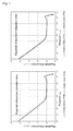
- FIG. 1 illustrates that the curve of the impedance value varied according to frequency is observed to have the same trend before and after PCR reaction, even though a particular target DNA template as a diagnostic sample exists.
- the change of the capacitance value (C d ) on the surface of a sensing electrode could be detected electrically after the PCR reaction between a primer fixed onto the sensing electrode and a template ssDNA.
- the change pattern of impedance curves might also be observed before and after the PCR reaction, because the change of the capacitance value (C d ) on the surface of the sensing electrode should be reflected after DNA amplification by the PCR reaction.
- the capacitance value (C d ) changed after reacting a sensing electrode and a biomolecule may be passed over by the capacitance value (C t ) between an imaginary electrode plate and another sensing electrode as described above, the impedance curve is not changed and just observed as a single curve before and after the PCR reaction, when being measured with an biochip-connected apparatus monitoring an impedance value (See FIG. 1 ).
- the capacitance value (C d ) changed by reacting a receptor immobilized onto an electrode and a biomolecule is passed over by the capacitance value (C t ) between an imaginary electrode plate and another sensing electrode containing a buffer solution as a dielectric substance, and thus, two curves of the changes of the impedance value which mean total change of the capacitance value (C T ) are not measured.
- C T capacitance value
- the present inventors have accomplished to design a method for detecting a biomolecule and a biochip therefor, wherein the dielectric constant of a material filled between electrodes within a reaction chamber of a biochip is made large, which does not distort actual change of the capacitance value when reacting on the surface of a sensing electrode, and thus, reflects accurately the biological, biochemical or chemical reaction of a biomolecule in a reaction chamber.
- the present invention aims to settle the above-mentioned disadvantage that cannot monitor sensitively a capacitance value changed in an electrode of a biosensor during actual reaction in prior arts.
- the object of the present invention is to provide a method for detecting the presence and/or the reaction of a biomolecule by accurately monitoring changes of electrical property after biological, biochemical or chemical reaction of a biomolecule in a reaction chamber and a biochip provided therefor.
- the object of the present invention is to provide a method for detecting changes of electrical property, especially changes of an impedance or capacitance value accurately after biological, biochemical or chemical reaction of a biomolecule in a reaction chamber, by using a sensing electrode installed in the reaction chamber and a biochip provided for this purpose.
- the object of the present invention is to provide a method for detecting a biomolecule and a biochip used for this purpose, wherein the dielectric constant of a material filled between electrodes within a reaction chamber of a biochip is made large, which does not distort actual changes of a capacitance value when reacting on the surface of a sensing electrode and thus, accurately reflects the biological, biochemical or chemical reaction of a biomolecule in a reaction chamber.
- the capacitance value is defined as described in the mathematical formula 4. Accordingly, the area of electrode should become larger, the interval between electrodes should become narrower, or the dielectric constant of a material filled between electrodes should become larger in order to increase C t score.
- the system for increasing sensing sensitivity in which the width of a sensor electrode is decreased in IDE (interdigitated electrode) of a biochip in order to increase C t , has adopted as described above.
- the decrease of electrode width may not be preferred in respect of cost and efficiency, since it requires a highly advanced microelectrode formation technique.
- the present invention has attempted a system for increasing dielectric constant ⁇ (or also referred to as dielectric ratio) of a material filled between electrodes in a reaction chamber of a biochip.
- This method does not require a highly advanced technique of microelectrode formation, as well as not distort actual changes of a capacitance value when reacting on the surface of a sensing electrode, and can accurately reflect the biological, biochemical or chemical reaction of a biomolecule in a reaction chamber.
- the biochip is filled with a reagent for reacting a target sample between electrodes of a reaction chamber. Accordingly, it is required to increase the dielectric constant of this reagent. But, this reagent for reacting a target sample is difficult to modulate the dielectric constant due to ions.
- the dielectric constant is defined as the ratio of the capacity measured when a dielectric substance is filled between electrodes to the capacity measured when nothing is filled between electrodes, and the dielectric ratio of any dielectric substance is always larger than 1.
- the dielectric constant of water is known to be largest and approximately 80 at room temperature.
- water such as distilled water or deionized water cannot be used for reagent use directly.
- the present invention provides a method for detecting the presence and/or the reaction of a biomolecule in a target sample, wherein the reaction of the target sample is performed under known reaction solution, in which a reference fluid having a high dielectric constant such as water is filled into a reaction chamber before the reaction to measure an impedance value or a capacitance value, after completing the reaction, the reaction solution is removed and said reference fluid having a high dielectric constant is refilled to measure an impedance value or a capacitance value, and then the impedance value or the capacitance value measured before and after the reaction is compared with each other.
- a reference fluid having a high dielectric constant such as water
- the present invention provides a method for detecting a biomolecule electrically, which comprises: (a) providing an apparatus for electrical detection comprising a reaction chamber receiving a target sample, and a plurality of sensing electrodes located in the reaction chamber for detecting a biomolecule within the target sample; (b) measuring an impedance value or a capacitance value between the sensing electrodes, after introducing a reference fluid having a high dielectric constant into the reaction chamber; (c) providing a reaction solution and the target sample into the reaction chamber, after removing the reference fluid having a high dielectric constant from the reaction chamber; (d) reacting the target sample under the reaction solution in the reaction chamber; (e) removing the reaction solution from the reaction chamber; (f) measuring an impedance value or a capacitance value between the sensing electrodes, after introducing said reference fluid having a high dielectric constant again into the reaction chamber; and (g) comparing the impedance value or the capacitance value measured in the step (b) with the impedance value or the capacitance value measured
- the impedance value or the capacitance value is measured according to frequency in the step (b) and the step (f), respectively by a measuring device using alternating current (AC) electric source.
- the impedance value or the capacitance value measured is illustrated as curves with respect to the frequency value.
- the curve of the impedance value or the capacitance value obtained in the step (b) is discriminated from the curve of the impedance value or the capacitance value obtained in the step (f), this result is judged to show the presence of the target biomolecule or the reaction of the target biomolecule onto the sensing electrode within the target sample.
- the reference fluid having a high dielectric constant is preferable to have approximately more than 4 of dielectric constant, more preferably to have approximately more than 80 of dielectric constant.
- the reference fluid having a high dielectric constant can be distilled water or deionized water, but the present invention is not limited hereto. Any fluid can be applicable, if it has approximately more than 4 of dielectric constant as described above.
- the sensing electrodes are preferably made of gold, chrome, copper or aluminum.
- the sensing electrodes are formed of interdigitated electrode, and each interval between the sensing electrodes can be approximately 1 to 20 ⁇ m and preferably, approximately 1 to 4 ⁇ m.
- a plurality of the sensing electrodes can be bound with a receptor capable of interacting with the biomolecule.
- biomolecule is a material that interacts with the receptor combined on the sensing electrode and can include nucleic acids comprising one or more nucleotides, proteins comprising one or more peptides, amino acids, glycolipids or small molecule compounds, and preferably an antigen, DNA, RNA or PNA (peptide nucleic acid).
- the term "receptor” is a material combined on the sensing electrode, which interacts with the biomolecule and can include nucleic acids comprising one or more nucleotides, proteins comprising one or more peptides, amino acids, glycolipids or small molecule compounds, and preferably an antigen, a probe or a primer.
- the receptor has a feature to be an oligonucleotide probe, the biomolecule is the nucleic acid, and the reaction solution is a solution for nucleic acid hybridization.
- the receptor has a feature to be an oligonucleotide primer, the biomolecule is the nucleic acid, and the reaction solution is a solution for PCR amplification.
- the biochip of the present invention used in the method for detecting a biomolecule can be manufactured in a form of single plate, but can be in a combined form of two plates.
- this biochip can include a DNA hybridization chip or a PCR reaction chip.
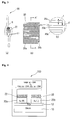
- the biochip having a combined form of two plates comprises a first plate that has a plurality of sensing electrodes bound with a receptor interacting with a biomolecule, and a second plate that forms a space of a reaction chamber with respect to the first plate by being combined with the first plate in a predetermined distance.
- the first plate has a plurality of sensing electrodes formed on SiO 2 insulation layer on N-type or P-type silicon plate, which performs electrical detection in order to identify whether a biomolecule exists and/or reacts or not.
- the second plate prevents the sensing electrodes of the first plate from contacting outside environment to form a space of a reaction chamber by being combined with the first plate.
- the reaction chamber is a space where an impedance value and/or a capacitance value are measured between electrodes after being filled with a reference fluid having a high dielectric constant.
- the reaction chamber is a space where a biomolecule in the target sample is reacted after being filled with the reaction solution and the target sample.
- the receptor is immobilized on the sensing electrode, the biomolecule within the reaction chamber reacts with the receptor and as a result, the changes of an impedance value and/or a capacitance value between electrodes occur.
- the above-mentioned plates can have various sizes, depending upon the kind and the number of applicable receptors, for example the kind and the number of probes and primers.
- the plates can have square shape, rectangular shape, and circular shape, but are not limited hereto in the present invention.
- the first plate may be a silicon plate
- the second plate may be a glass plate.
- these plates can be also constructed by any one selected from the group consisting of glass, silicon, fused silica, polystylene, polymethylacrylate, polycarbonate, gold, silver, copper and platinum.
- the second plate forming the space of the reaction chamber is perforated to have a fluid inlet in the direction of thickness and further perforated to have a fluid outlet in the direction of thickness on the opposite side of the fluid inlet.
- the inlet and the reaction chamber, and the outlet and the reaction chamber are communicated with each other to allow fluid to flow therethrough in the reaction chamber.
- the reference fluid having a high dielectric constant, the reaction solution and the target sample are introduced through the inlet, and the reference fluid having a high dielectric constant, the reaction solution and the target sample flow outside through the outlet.
- an inlet micro channel that directs to introduce fluid into the inlet, and an outlet micro channel that directs to discharge fluid from the outlet can be made by layering a third plate on the second plate.
- the inlet micro channel is communicated with an injection opening into which the reference fluid having a high dielectric constant, the reaction solution and the target sample are injected, and penetrates through the third plate.
- the outlet micro channel is communicated with a discharge opening into which the reference fluid having a high dielectric constant, the reaction solution and the target sample are discharged, and penetrates through the third plate.
- a valve structure that can control fluid injection into the space of the reaction chamber and fluid discharge from the space of the reaction chamber can be provided on the inlet micro channel and/or the outlet micro channel.
- the valve structure is a passage extended after being penetrated into the third plate in the direction of thickness, between the injection opening and the space of the reaction chamber, or between the discharge opening and the space of the reaction chamber wherein oil is stored in said passage.
- nitrogen gas (N 2 ) is injected into this passage of the valve structure, the oil stored in the passage expands and blocks the channels due to the oil expansion so as to obstruct inflow of fluid from the injection opening to the reaction chamber and outflow of fluid from the reaction chamber to the discharge opening.
- the third plate is made of PDMS (polydimethylsiloxane).
- micro channel and the valve structure mentioned above can be prepared in a micron unit or nano unit by using a MEMS (micro-electro-mechanical-system) technique used widely in this field, and their size can be controlled, depending upon receptor size, electrode size, or reaction condition.
- MEMS micro-electro-mechanical-system
- the channel structure and the valve structure facilitate following steps in the above-mentioned method: filling the reference fluid having a high dielectric constant into the reaction chamber before reaction; removing the reference fluid having a high dielectric constant from the reaction chamber and filling the reaction solution and the target sample into the reaction chamber during reaction; and removing the reaction solution from the reaction chamber and refilling the reference fluid having a high dielectric constant into the reaction chamber after the reaction.
- the biochip can be provided with an injection pump and a discharge pump in order to inject and remove the fluid, the reaction solution and the target sample.
- the biochip can also be provided with a small motor or a gearbox.
- an impedance analyzer can be connected electrically to a plurality of sensing electrodes.
- this biochip is a PCR reaction chip
- a PCR device for conducting PCR reaction can be manufactured to accommodate a biochip and thus, the biochip and the PCR device can be provided as one set.
- the PCR device having an impedance measuring apparatus is used and the impedance measuring apparatus is connected electrically to sensing electrodes of the biochip.
- the method of present invention can detect the change of electrical property accurately according to biological, biochemical or chemical reactions of the biomolecule within the reaction chamber, even though the capacitance value (C d ) changed on the surface of sensing electrodes may be passed over by the capacitance value (C t ) of the buffer solution.
- the present invention is advantageous to make the dielectric constant of a material filled between electrodes within the reaction chamber of the biochip large, which does not distort actual change of a capacitance value when reacting the biomolecule in the target sample with the receptors immobilized on the surface of sensing electrodes, and can reflect total change of the capacitance value accurately and thus, detect the presence and/or the reaction of the biomolecule sensitively.
- a target biomolecule is DNA and a receptor combining with a sensing electrode is an oligonucleotide probe, a DNA hybridization chip for hybridizing a probe and DNA as a biomolecule is prepared.
- the DNA hybridization chip sensor is manufactured by using a general procedure disclosed in this field, including thin film formation technique of silicon dioxide, photolithography technique, exposure patterning technique, developing technique, wet and/or dry etching technique, etc. Particularly, sensing metal electrodes having an IDE (interdigitated electrode) are formed on a silicon plate by using a MEMS (micro-electro-mechanical-systems) and then, oligonucleotide probes are immobilized on the sensing electrodes.
- IDE interdigitated electrode
- MEMS micro-electro-mechanical-systems
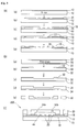
- Example 1-1 Construction of a silicon plate on which electrodes are formed
- N-type silicon wafer (10) having 500 ⁇ m of thickness was thermally oxidized to make about 10,000 of a SiO 2 layer (12), an oxidized insulation layer (See the Step (a) of FIG. 2 ). Then, the insulation layer (12) was coated with a photoresist AZ 5214 (14) (See the Step (b) of FIG. 2 ). On the photoresist (14), a mask having a pattern of metal electrodes (not shown) was mounted and exposed with ultra violet light. After that, the silicon wafer (10) was immersed in AZ300MIF developing solution to be developed and etch-treated (See the Step (c) of FIG. 2 ).
- a thin film (20) of chrome (Cr) (300 ) and gold (Au) (3000) was deposited (See the Step (d) of FIG. 2 ).
- the deposition of the thin film (20) of chrome and gold was performed by using chemical vapor deposition (CVD), vacuum evaporation or sputtering.
- CVD chemical vapor deposition
- the photoresist layer (14) remained and a part of the thin film on the photoresist layer (14) remained were removed by using a known lift-off process so as to make a metal electrode (20) (See the Step (e) of FIG. 2 ).
- a photoresist AZ4620 (16) was additionally coated and the electrode (20) was patterned to form a fine IDE by using a known photolithography procedure in this field (See the Step (f) of FIG. 2 ).
- the DNA hybridization chip (100) manufactured is illustrated in FIG. 3 .
- the DNA hybridization chip (100) depicted in FIG. 3 (a) has approximately 2.4 mm of diameter (R) in the electrode (20), but is better to have as small diameter as possible in order to manufacture an electrode array type DNA hybridization chip (See FIG. 7 ).
- the area of the electrode (20) is approximately 3.6 mm 2 .
- FIG. 3 (b) the electrode depicted in FIG. 3 (a) is magnified partially and illustrated schematically.
- the shape of the electrode (20) is illustrated with a rectangle, but an actual electrode (20) may be round or elliptic.
- the sensing electrodes (20) of the DNA hybridization chip (100) used in the present invention have a pair of electrodes (20a, 20b) wherein they are arrayed alternately in a predetermined interval with a finger-like shape.
- each electrode (20a, 20b) having a finger-like shape is magnified partially as illustrated in FIG. 3 (c) .
- the width (t) of each electrode (20a, 20b) is approximately 10 ⁇ m and the interval (d) between the electrodes is approximately 4 ⁇ m.
- Example 1-2 Immobilization of oligonucleotide probes on an electrode
- the electrodes (20) of the DNA hybridization chip (100) prepared in Example 1-1 were washed with oxygen plasma (150 W, 100 mtorr) for 10 seconds in order to remove impurities on the electrodes (20) completely. Then, one end of a probe DNA (5' or 3') was immobilized on the electrode (20). For this immobilization, a probe 5'-SH-(CH 2 ) 24 -GCC ATT CTC ACC GGA TTC AGT CGT C-3', in which a thiol group is attached to a carbon chain (-CH 2 -) at the 5'terminus of the probe oligonucleotide, is prepared and fixed on the surface of the metal electrode (20) by using a SAM (self-assembled method).
- SAM self-assembled method
- a conductive polymer can be bound to a probe DNA instead of a thiol group, and the conductive polymer bound to DNA can be immobilized onto the surface of the metal electrode by using a SAM method (self assembled method).
- All the conductive polymers known in this field for example, especially high-conductive polymer including polyacetylene, poly(p-phenylene) (PPP), polypyrrole (PPy), polyaniline, polythiophene, etc. may be used.
- the conductive polymer can be bound to the probe DNA by using a known binding method regarding binding between a polymer and DNA.
- FIG. 4 is a cross sectional view of the metal electrode (20) of FIG. 3 (b) sectioned according to A-A' line and illustrates the immobilization of the DNA probes (22) on the metal electrodes (20a, 20b) formed on the silicon plate wherein the oxidized insulation layer (12) intervenes between the metal electrodes (20a, 20b) and the silicon plate (10).
- Example 2 Detection of a target nucleotide sequence using the DNA hybridization chip
- the DNA hybridization chip (100) of FIG. 4 manufactured in Example 1-2 was used to examine whether a target nucleotide sequence (5'-GAC GAC TGA ATC CGG TGA GAA TGG-3') is found within a target sample or not.
- deionized water as a reference solution having a high dielectric constant was introduced into a reaction space between electrodes (20) of the DNA hybridization chip (100) and then, the impedance value between the electrodes (20) was measured at room temperature by applying AC power.
- the applied magnitude of AC power was 100 mV and its frequency range was 1 to 32 MHz when the impedance value was measured.
- the reference solution was removed from the DNA hybridization chip (100) and then, the target sample containing the target nucleotide sequence (10 pmol/ of ssDNA) and TE buffer were introduced into the reaction space of the DNA hybridization chip (100).
- the resultant was incubated for 18 hours at room temperature depending upon hybridization condition to hybridize the probe DNA (22) immobilized onto the electrode (20) of the DNA hybridization chip (100) with ssDNA of the target nucleotide sequence (5'-GAC GAC TGA ATC CGG TGA GAA TGG-3').
- the buffer solution was removed from the DNA hybridization chip (100) and deionized water was introduced. Then, the impedance value between the electrodes (20) was measured at room temperature by applying AC power. The applied magnitude of AC power was 100 mV and its frequency range was 1 to 32 MHz when the impedance value was measured.
- the impedance value measured before the hybridization reaction and the impedance value measured after the hybridization reaction are illustrated in FIG. 8 .
- FIG. 8 contrasting to FIG. 1 in case of a conventional method, the impedance value measured before the hybridization reaction and the impedance value measured after the hybridization reaction were observed with two different curves, when this experiment is conducted by using a positive target sample containing the target nucleotide sequence.
- the impedance value should decrease when the target DNA exists in the reaction solution during the hybridization reaction. Therefore, it is confirmed that the impedance value will decrease as the conductance value increases due to the hybridization from ss-DNA to ds-DNA during the hybridization reaction.
- the change of the capacitance value (C d ) after hybridizing a target ssDNA with a probe immobilized on a sensing electrode should reflect total change of the capacitance value (C T ) since it is not passed over by the capacitance value (C t ) of a buffer solution.
- the method of the present invention can permit electrical monitoring to detect the hybridization reaction and the presence of target DNA, because two curves of the changes of the impedance value are observed before and after the hybridization as shown in FIG. 8 .
- the impedance value measured from a negative target sample without a target nucleotide sequence should be smaller than the impedance value of the positive case as shown in FIG. 8 .
- a target biomolecule is DNA and a receptor combining with a sensing electrode is an oligonucleotide primer
- a PCR reaction chip for amplifying DNA as a target biomolecule by using a primer and a PCR reagent is manufactured.
- the PCR reaction chip is also manufactured by using a general procedure disclosed in this field.
- a silicon plate and an electrode portion can be manufactured by using thin film formation technique of silicon dioxide, photolithography technique, exposure patterning technique, developing technique, wet and/or dry etching technique, etc.
- the sensing metal electrodes having an IDE (interdigitated electrode) are formed on the silicon plate by using a MEMS (micro-electro-mechanical-systems) and then, the oligonucleotide primers are immobilized on the sensing electrodes.
- a glass plate attached to the silicon plate is made by using glass wet etching and sand blasting technique.
- Example 3-1 Construction of a silicon plate, electrodes and a glass plate
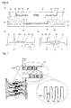
- N-type silicon wafer (10) having 500 ⁇ m of thickness was thermally oxidized to make about 5,000 of a SiO 2 layer (12), an oxidized insulation layer (See the Step (a) of FIG. 5A ).
- Ti/Au (300 /3000 ) metal electrode (20) was patterned by using a conventional photolithography process, and a part of the electrode, which will be excluded from an IDE, was removed to form a fine IDE by dry-etching using ion milling (See the Step (b) of FIG. 5A ).
- a SiO 2 layer (18) of at least 1 ⁇ m of thickness was deposited onto the patterned metal electrode (20) by using chemical vapor deposition (CVD), vacuum evaporation or sputtering, etc.
- CVD chemical vapor deposition
- the SiO 2 layer (18) of the insulation layer was made even by using chemical mechanical polishing (CMP) (See the Step (d) of FIG. 5A ).
- CMP chemical mechanical polishing
- the IDE was only treated with dry etching (RIE) or wet etching (BOE) to expose the surface of Au metal electrode.
- RIE dry etching
- BOE wet etching
- the pattern of the metal electrode (20) is similar to that of the DNA hybridization chip (100) as shown in FIG. 3 (a) , and a pair of electrodes (20a, 20b) is arrayed alternately in a predetermined interval with a finger-like shape.
- the electrode (20) has approximately 8.6 mm of diameter, but it is better to have as small diameter as possible in order to manufacture an electrode array type PCR reaction chip (See FIG. 7 ).
- the width (t) of each electrode (20a, 20b) is approximately 20 ⁇ m and the interval (d) between the electrodes is approximately 20 ⁇ m.
- Cr/Au (300/3000) metal film (32) was deposited on the upper and the lower surfaces of a conventional glass plate (Pyrex product) (30) used in a semiconductor process by using chemical vapor deposition (CVD), vacuum evaporation or sputtering, etc. (See the Step (a) of FIG. 5B ).
- CVD chemical vapor deposition
- a thin metal film (32) formed on the upper portion was patterned and wet-etched to form a protective layer (32) that is a part for protecting a glass plate portion processed later (See the Step (b) of FIG. 5B ).
- the other portion of the glass plate (30) that is not protected by the protective layer (32) was wet-etched to form a space of a reaction chamber in the PCR reaction chip (See the Step (c) of FIG. 5B ).
- All the thin metal films formed on the upper and the lower surfaces were removed and the bottom surface of the glass plate was treated with a blue tape (any blue tape is available if suitable for patterning) patterning (34) in order to form an inlet/outlet (36a, 36b) of the PCR reaction chip (See the Step (d) of FIG. 5B ).
- penetration openings including inlet/outlet openings, etc. were made in the direction of thickness on the glass plate (30) by performing a sand blast process known in this field (See the Step (e) of FIG. 5B ).
- the silicon plate (10) previously manufactured on which the metal electrodes (20) are formed was bound with the glass plate (30) by using anodic bonding as illustrated in FIG. 5C .
- the resulting silicon plate (10) and glass plate (30) was diced to obtain a final PCR reaction chip (200).
- the anodic bonding is a method for binding a silicon plate and a glass plate, in which cationic ions (for example, Na + ion) present within a glass plate are allowed to move to the opposite direction with respect to the position where the silicon plate and the glass plate are earthed, to form hydrogen bonds on the surfaces of the silicon plate and the glass plate and to bind the two plates by applying hot heat and high electric field.
- cationic ions for example, Na + ion
- a plurality of metal sensing electrodes (20) are formed on the silicon plate (10) (See FIG. 5 and FIG. 6A ), and primers (22) for a target DNA template are immobilized on the electrodes (See FIG. 6A ).
- this silicon plate (10) is bound to the glass plate (30) in a predetermined distance to form a space for a reaction chamber (46) (See FIG. 5 and
- FIG. 6A is a diagrammatic representation of FIG. 6A .
- the space of the reaction chamber (46) is a space where the impedance value is measured between the electrodes after being filled with a reference solution of deionized water. Also, the space of the reaction chamber (46) is a space that accommodates a target sample and a PCR reaction solution to conduct a PCR reaction, in which the target DNA template present in the target sample binds complementarily to the primers (22) immobilized on the metal electrodes (20) of the silicon plate (10) to proceed the PCR reaction.
- the change of the impedance value between the metal electrodes (20) according to PCR reaction will be detected to monitor whether the target DNA template is present within the target sample or not.
- the glass plate (30) plays a role to protect the space of the reaction chamber (46) from outside environment.
- the glass plate (30) is perforated to have a fluid inlet (36a) in the direction of thickness and further perforated to have a fluid outlet (36b) in the direction of thickness on the opposite side of the fluid inlet (36a) (See FIG. 5 and FIG. 6A ).
- the inlet (36a) and the space of the reaction chamber (46), and the outlet (36b) and the space of the reaction chamber (46) are communicated with each other to allow fluid to flow therethrough in the reaction chamber (46).
- the reference solution of deionized water, the PCR reaction solution and the target sample are introduced into the reaction chamber (46), and the reference solution of deionized water, the PCR reaction solution and the target sample are discharged from the reaction chamber (46) through the outlet (36b).
- a fluid controlling plate (40) based upon PDMS is prepared and attached onto the glass plate (30) of the PCR reaction chip (200) manufactured previously.
- the fluid controlling plate (40) of the PCR reaction chip (200) used in the present invention is preferable to be prepared with a transparent polymer in order to allow the inside of the chip (200) to be seen.
- PDMS polydimethylsiloxane
- PDMS is cheaper than silicone and easy to be manipulated, flexible and resistant to water when bound to another surfaces.
- PDMS does not cause any negative effect upon biomolecules due to its biocompatible property.
- it is preferably deposited with a reactive coating material or treated with graft copolymerization. Non-specific adsorption of hydrophobic components of cell such as protein may occur, if not coated.
- channels (44a, 44b) and a discharge opening (48) are coated with bovine serum albumin (BSA) in the fluid controlling plate (40), the non-specific adsorption of hydrophobic components can be minimized.
- BSA bovine serum albumin
- the fluid controlling plate (40) was designed by using a CAD (computer aided design) program. Then, the resulting design was printed on a photomask and impurities were removed. SU-8 of a negative type photoresist was spin-coated on the silicon wafer.
- a template for the fluid controlling plate (40) was manufactured by exposure and development using a photomask that has patterns of an injection opening (42), a valve structure (52), micro channels (44a, 44b) and a discharge opening (48). And then, PDMS of liquid phase was poured into the SU-8 template, solidified by heating and separated from the template.
- the resulting PDMS fluid controlling plate (40) was cut according to the size of the PCR reaction chip (200) and perforated at the position, where the injection opening (42) and the discharge opening (48), etc. were formed, in a desired size by using a punch. After that, the fluid controlling plate (40) as manufactured above was oxidized with plasma and then, attached to the corresponding position on the glass plate (30) of the PCR reaction chip (200).
- FIG. 6A illustrates a longitudinal sectional view of the finally manufactured PCR reaction chip (200) to which the fluid controlling plate (40) is attached.
- an inlet micro channel (44a) that directs to introduce fluid into the inlet (36a), and an outlet micro channel (44b) that directs to discharge fluid from the outlet (36b) are formed.
- An injection opening (42) that introduces a reference solution of deionized water, a PCR reaction solution and a target sample is formed in the fluid controlling plate (40), by being penetrated into the fluid controlling plate.
- the injection opening (42) can introduce fluid into the reaction chamber (46) since it is communicated with the inlet micro channel (44a).
- a discharge opening (48) that discharges a reference solution of deionized water, a PCR reaction solution and a target sample is formed in the fluid controlling plate (40), by being penetrated into the fluid controlling plate.
- the discharge opening (48) can discharge fluid from the reaction chamber (46) since it is communicated with the outlet micro channel (44b).
- passages (52) extended longitudinally after being penetrated into the fluid controlling plate (40) in the direction of thickness, between the injection opening (42) and the reaction chamber (46), or between the discharge opening (48) and the reaction chamber (46) are formed in the fluid controlling plate (40) (See FIG 6. (A) and (B) ).
- the passage (52) plays a role of valve for the inlet micro channel (44a) and/or the outlet micro channel (44b).
- Silicone oil (50) is stored in the extended passage (52).
- nitrogen gas (N 2 ) is injected into the passage (52) in which the silicone oil (50) is stored, the oil (50) stored in the passage (52) expands and blocks the channels (44a, 44b) due to the oil expansion. Therefore, the fluid controlling plate (40) can block and control inflow of fluid from the injection opening (42) to the reaction chamber (46), and outflow of fluid from the reaction chamber (46) to the discharge opening (48).
- Example 3-2 Immobilization of oligonucleotide primers on an electrode
- the electrode (20) of the PCR reaction chip (200) manufactured in Example 3-1 was washed for 30 minutes by using Pirahna solution (mixture of H 2 SO 4 and H 2 O 2 in 70 : 30) to completely remove impurities on the electrode (20).
- one end (5' or 3') of the upstream primer and one end (5' or 3') of the downstream primer were immobilized on the electrode (20). Both the upstream primer and the downstream primer can be immobilized on the electrode (20), otherwise one end of any primer can be immobilized on the electrode and one end of the other primer can be mixed in a PCR reaction solution to perform a PCR reaction.
- the -SH group of the primer is reacted with the metal surface to immobilize the primer ssDNA (22) on the surface of the metal electrode (20).
- the immobilization process onto the metal surface performed in this example is substantially identical with that in example 1-2, as shown in FIG. 4 .
- Example 4 Analysis of PCR reaction by using a PCR reaction chip
- the PCR reaction chip (200) on which primers are immobilized as manufactured in Example 3-2 was used to examine whether a target DNA template is found within a target sample and a PCR reaction is performed or not.
- deionized water of a reference solution having a high dielectric constant was introduced into the reaction chamber (46) of the PCR reaction chip (200) and then, the impedance value between the electrodes (20) was measured at room temperature by applying AC power.
- the applied magnitude of AC power was 100 mV and its frequency range was 1 to 32 MHz when the impedance value was measured.
- the PCR reaction solution was completely removed from the PCR reaction chip (200) and deionized water was introduced into the reaction chamber. Then, the impedance value between the electrodes (20) was measured at room temperature by applying AC power. The applied magnitude of AC power was 100 mV and its frequency range was 1 to 32 MHz when the impedance value was measured.
- the impedance value measured before and after the PCR reaction is illustrated in FIG. 9 .
- FIG. 9 contrasting to FIG. 1 in case of a conventional method, the impedance value measured before the PCR reaction and the impedance value measured after the PCR reaction were observed with two different curves, when this experiment is conducted by using a positive target sample containing the target DNA template.
- the impedance value should decrease when the target DNA template exists in the reaction solution during the PCR reaction. Therefore, it is confirmed that the impedance value will decrease as the conductance value increases due to the PCR reaction from ss-DNA to ds-DNA during the PCR reaction.
- the change of the capacitance value (C d ) after amplifying a target DNA template with PCR primers immobilized on a sensing electrode should reflect total change of the capacitance value (C T ) since it is not passed over by the capacitance value (C t ) of a buffer solution.
- the method of the present invention can permit electrical monitoring to detect the PCR reaction and the presence of the target DNA template, because two curves of the changes of the impedance value are observed before and after the PCR reaction, as shown in FIG. 9 .
- the impedance value measured from a negative target sample without a target DNA template should be smaller than the impedance value of the positive case as shown in FIG. 9 .
Landscapes
- Health & Medical Sciences (AREA)
- Life Sciences & Earth Sciences (AREA)
- Immunology (AREA)
- Chemical & Material Sciences (AREA)
- Molecular Biology (AREA)
- Engineering & Computer Science (AREA)
- Physics & Mathematics (AREA)
- Biochemistry (AREA)
- Pathology (AREA)
- General Physics & Mathematics (AREA)
- General Health & Medical Sciences (AREA)
- Analytical Chemistry (AREA)
- Urology & Nephrology (AREA)
- Hematology (AREA)
- Biomedical Technology (AREA)
- Medicinal Chemistry (AREA)
- Food Science & Technology (AREA)
- Chemical Kinetics & Catalysis (AREA)
- Electrochemistry (AREA)
- Biotechnology (AREA)
- Cell Biology (AREA)
- Microbiology (AREA)
- Spectroscopy & Molecular Physics (AREA)
- Investigating Or Analyzing Materials By The Use Of Electric Means (AREA)
- Apparatus Associated With Microorganisms And Enzymes (AREA)
Applications Claiming Priority (2)
| Application Number | Priority Date | Filing Date | Title |
|---|---|---|---|
| KR1020080027099A KR100969667B1 (ko) | 2008-03-24 | 2008-03-24 | 생리활성물질을 전기적으로 검출하는 방법 및 이를 위한바이오칩 |
| PCT/KR2009/000285 WO2009119971A2 (fr) | 2008-03-24 | 2009-01-20 | Procédé de détection électrique de matériaux physiologiquement actifs, et biopuce pour ce procédé |
Publications (3)
| Publication Number | Publication Date |
|---|---|
| EP2273263A2 true EP2273263A2 (fr) | 2011-01-12 |
| EP2273263A4 EP2273263A4 (fr) | 2011-05-11 |
| EP2273263B1 EP2273263B1 (fr) | 2013-03-20 |
Family
ID=41114429
Family Applications (1)
| Application Number | Title | Priority Date | Filing Date |
|---|---|---|---|
| EP09724909A Active EP2273263B1 (fr) | 2008-03-24 | 2009-01-20 | Procédé de détection électrique de matériaux physiologiquement actifs, et biopuce pour ce procédé |
Country Status (6)
| Country | Link |
|---|---|
| US (2) | US8354307B2 (fr) |
| EP (1) | EP2273263B1 (fr) |
| JP (1) | JP5371061B2 (fr) |
| KR (1) | KR100969667B1 (fr) |
| CN (1) | CN101981445B (fr) |
| WO (1) | WO2009119971A2 (fr) |
Cited By (2)
| Publication number | Priority date | Publication date | Assignee | Title |
|---|---|---|---|---|
| WO2012028719A3 (fr) * | 2010-09-02 | 2012-06-07 | Heed Diagnostics Aps | Détection électrochimique d'un analyte |
| TWI620932B (zh) * | 2016-06-08 | 2018-04-11 | 立錡科技股份有限公司 | 生醫檢測裝置以及生醫檢測裝置之製造方法 |
Families Citing this family (28)
| Publication number | Priority date | Publication date | Assignee | Title |
|---|---|---|---|---|
| EP1648286B1 (fr) | 2003-07-12 | 2017-12-20 | Accelerate Diagnostics, Inc. | Biodetection sensible et rapide |
| US20120077206A1 (en) | 2003-07-12 | 2012-03-29 | Accelr8 Technology Corporation | Rapid Microbial Detection and Antimicrobial Susceptibility Testing |
| ES2694080T3 (es) * | 2010-06-09 | 2018-12-17 | Apex Biotechnology Corp. | Dispositivo y método para medir el tiempo de protrombina y hematocrito mediante el análisis del cambio de reactancia en una muestra |
| KR101726238B1 (ko) * | 2010-10-15 | 2017-04-12 | (주) 하임바이오텍 | 표적 폴리뉴클레오티드의 염기서열을 비특이적으로 연장하는 방법, 이를 위한 프라이머 조성물 및 표적 폴리뉴클레오티드 검출감도 향상용 키트 |
| KR20120045909A (ko) * | 2010-11-01 | 2012-05-09 | 엘지전자 주식회사 | 복수 종의 표적 핵산을 실시간으로 검출하는 장치 및 방법 |
| KR101667648B1 (ko) * | 2010-12-01 | 2016-10-20 | (주) 하임바이오텍 | 전도성 입자를 이용하여 표적 폴리뉴클레오티드를 전기적으로 검출하는 방법 및 이를 위한 바이오 칩 |
| US10254204B2 (en) | 2011-03-07 | 2019-04-09 | Accelerate Diagnostics, Inc. | Membrane-assisted purification |
| ES2551922T3 (es) | 2011-03-07 | 2015-11-24 | Accelerate Diagnostics, Inc. | Sistemas rápidos de purificación celular |
| KR101729489B1 (ko) | 2011-03-11 | 2017-04-24 | (주) 하임바이오텍 | 전도성 입자들과 이에 대응하는 폴리뉴클레오티드들의 조합을 이용한 바이오 센서 및 이를 이용하여 전기적 신호를 검출하는 방법 |
| EP2807475A4 (fr) * | 2012-01-27 | 2015-10-07 | Univ Tennessee Res Foundation | Procédés et appareil de détection d'un biomarqueur par électrocinétique en courant alternatif |
| US9677109B2 (en) | 2013-03-15 | 2017-06-13 | Accelerate Diagnostics, Inc. | Rapid determination of microbial growth and antimicrobial susceptibility |
| EP3000088A4 (fr) | 2013-05-23 | 2018-06-27 | Iphenotype LLC | Procédé et système pour maintenir ou améliorer le bien-être |
| US10167501B2 (en) * | 2014-06-12 | 2019-01-01 | Auckland Uniservices Limited | Methods and apparatus for quantification of nucleic acid amplification by monitoring impedances |
| EP4109095A1 (fr) | 2014-09-09 | 2022-12-28 | Perosphere Technologies Inc. | Test de coagulation universel fondé sur une puce microfluidique |
| US10196678B2 (en) | 2014-10-06 | 2019-02-05 | ALVEO Technologies Inc. | System and method for detection of nucleic acids |
| KR101709762B1 (ko) * | 2015-02-09 | 2017-02-23 | 광운대학교 산학협력단 | 생체분자 농축 기능 일체형 센서 및 그 제조방법 |
| EP3278115A2 (fr) | 2015-03-30 | 2018-02-07 | Accelerate Diagnostics, Inc. | Instrument et système pour l'identification rapide de micro-organismes et test de la sensibilité à un agent antimicrobien |
| US10253355B2 (en) | 2015-03-30 | 2019-04-09 | Accelerate Diagnostics, Inc. | Instrument and system for rapid microorganism identification and antimicrobial agent susceptibility testing |
| KR101754239B1 (ko) * | 2015-12-28 | 2017-07-06 | 한국과학기술연구원 | 수용체와 표적 생체물질의 반응을 이용한 교차 전극 바이오센서 |
| KR101727107B1 (ko) | 2016-02-19 | 2017-04-17 | 한국과학기술연구원 | 유전체 전기영동을 이용한 마이크로 전극 바이오 센서 |
| US10012645B2 (en) * | 2016-08-24 | 2018-07-03 | The Florida International University Board Of Trustees | Rapid zika virus detection using nano-enabled electrochemical sensing system |
| US11465141B2 (en) * | 2016-09-23 | 2022-10-11 | Alveo Technologies, Inc. | Methods and compositions for detecting analytes |
| KR101912890B1 (ko) * | 2016-10-04 | 2018-10-29 | 한국과학기술연구원 | 표적 생체물질과 수용체의 반응을 개선한 교차 전극 바이오센서 |
| US11480567B2 (en) | 2017-02-15 | 2022-10-25 | New Jersey Institute Of Technology | Enhanced sensitivity and specificity for point-of-care (POC) micro biochip |
| US11020740B2 (en) * | 2017-10-24 | 2021-06-01 | New Jersey Institute Of Technology | Microfluidic biochip with enhanced sensitivity |
| CN110385150A (zh) * | 2018-04-19 | 2019-10-29 | 成功大学 | 介电微粒操控芯片 |
| WO2020032958A1 (fr) * | 2018-08-09 | 2020-02-13 | Hewlett-Packard Development Company, L.P. | Commande de chambre réactionnelle basée sur la conductivité |
| CN113970670B (zh) * | 2021-09-29 | 2022-08-09 | 西安电子科技大学 | 箔条空气混合介电常数测量方法、系统、设备、介质及终端 |
Citations (2)
| Publication number | Priority date | Publication date | Assignee | Title |
|---|---|---|---|---|
| WO2002055198A2 (fr) * | 2000-11-06 | 2002-07-18 | Nanostream Inc | Régulateurs de débits microfluidiques |
| WO2008016703A1 (fr) * | 2006-08-02 | 2008-02-07 | The Regents Of The University Of Michigan | Dispositifs et procédés d'actionnement de soupape hydraulique multiplexés |
Family Cites Families (26)
| Publication number | Priority date | Publication date | Assignee | Title |
|---|---|---|---|---|
| US4023096A (en) * | 1976-02-17 | 1977-05-10 | Shell Oil Company | Method and apparatus for determining physical characteristics of emulsions |
| JPS63231256A (ja) * | 1987-03-19 | 1988-09-27 | Jeol Ltd | イオン選択性電極を用いた検体電解質測定の校正デ−タ処理法 |
| US5587128A (en) * | 1992-05-01 | 1996-12-24 | The Trustees Of The University Of Pennsylvania | Mesoscale polynucleotide amplification devices |
| CA2250212C (fr) * | 1996-04-03 | 2010-02-09 | The Perkin-Elmer Corporation | Dispositif et procede de detection d'une pluralite d'analytes |
| GB9622304D0 (en) * | 1996-10-26 | 1996-12-18 | Univ Manchester | Sensor |
| US6686150B1 (en) * | 1998-01-27 | 2004-02-03 | Clinical Micro Sensors, Inc. | Amplification of nucleic acids with electronic detection |
| US6290839B1 (en) * | 1998-06-23 | 2001-09-18 | Clinical Micro Sensors, Inc. | Systems for electrophoretic transport and detection of analytes |
| US6169394B1 (en) * | 1998-09-18 | 2001-01-02 | University Of The Utah Research Foundation | Electrical detector for micro-analysis systems |
| CN1129669C (zh) * | 2000-08-18 | 2003-12-03 | 莫志宏 | 原位生物芯片及其制备方法 |
| KR100438828B1 (ko) * | 2001-11-08 | 2004-07-05 | 삼성전자주식회사 | 칩 상의 전기적 미세 검출기 |
| DE10211358B4 (de) * | 2002-03-14 | 2006-10-26 | Siemens Ag | Vertikal-Impedanz-Sensor-Anordnung und Verfahren zum Herstellen einer Vertikal-Impedanz-Sensor-Anordnung |
| US20040110277A1 (en) | 2002-04-12 | 2004-06-10 | Seiko Epson Corporation | Sensor cell, bio-sensor, capacitance element manufacturing method, biological reaction detection method and genetic analytical method |
| AU2003267998A1 (en) * | 2002-07-20 | 2004-02-09 | Acea Biosciences, Inc. | Impedance based devices and methods for use in assays |
| KR100858080B1 (ko) | 2002-11-12 | 2008-09-10 | 삼성전자주식회사 | 전기적 신호를 측정하는 pcr 증폭 산물을 검출하는 방법 |
| ATE544867T1 (de) * | 2002-12-11 | 2012-02-15 | Centre Nat Rech Scient | Methode zur elektronischen detektion wenigstens einer spezifischen interaktion zwischen einem proben- und einem zielmolekül |
| DE10324912A1 (de) * | 2003-05-30 | 2005-01-05 | Siemens Ag | Verfahren zur Detektion von DNA-Punktmutationen (SNP-Analyse) sowie zugehörige Anordnung |
| DE10328136A1 (de) | 2003-06-23 | 2005-01-27 | Infineon Technologies Ag | Sensor-Element, Sensor-Array und Verfahren zum Erfassen von in einem Analyten möglicherweise enthaltenen Partikeln |
| US20050059105A1 (en) * | 2003-07-25 | 2005-03-17 | Board Of Trustees Of Michigan State University | Impedimetric biosensor and its use for rapid detection of bacterial pathogens in solution |
| CN1860366A (zh) * | 2003-09-29 | 2006-11-08 | 皇家飞利浦电子股份有限公司 | 免标记检测生物分子 |
| US6990849B2 (en) | 2004-03-26 | 2006-01-31 | Lifescan, Inc. | Microfluidic analytical system with position electrodes |
| US20050266571A1 (en) | 2004-03-26 | 2005-12-01 | Phil Stout | Method for feedback control of a microfluidic system |
| KR100613612B1 (ko) * | 2004-04-27 | 2006-08-18 | 삼성전자주식회사 | 인덕턴스 소자 및 캐패시턴스 소자를 이용한 바이오결합검출 장치 및 방법 |
| WO2007040558A2 (fr) * | 2004-11-19 | 2007-04-12 | The Trustees Of Boston College | Procedes de fabrication de nanofils et d'electrodes avec nanotrous |
| JP4806548B2 (ja) * | 2005-03-10 | 2011-11-02 | 長野計器株式会社 | マイクロ流路の流体制御構造、マイクロ流路の流体制御構造の製造方法、および閉塞部材操作装置 |
| JP4616124B2 (ja) * | 2005-08-23 | 2011-01-19 | セイコーインスツル株式会社 | マイクロリアクタ、マイクロリアクタシステム、および該マイクロリアクタシステムを用いた分析方法 |
| JP4660768B2 (ja) * | 2006-03-28 | 2011-03-30 | 国立大学法人 筑波大学 | 微小分析装置及び微少試料の分析方法 |
-
2008
- 2008-03-24 KR KR1020080027099A patent/KR100969667B1/ko active IP Right Grant
-
2009
- 2009-01-20 US US12/922,934 patent/US8354307B2/en active Active
- 2009-01-20 EP EP09724909A patent/EP2273263B1/fr active Active
- 2009-01-20 WO PCT/KR2009/000285 patent/WO2009119971A2/fr active Application Filing
- 2009-01-20 CN CN2009801108754A patent/CN101981445B/zh active Active
- 2009-01-20 JP JP2010549557A patent/JP5371061B2/ja active Active
-
2012
- 2012-12-07 US US13/708,236 patent/US9005545B2/en active Active
Patent Citations (2)
| Publication number | Priority date | Publication date | Assignee | Title |
|---|---|---|---|---|
| WO2002055198A2 (fr) * | 2000-11-06 | 2002-07-18 | Nanostream Inc | Régulateurs de débits microfluidiques |
| WO2008016703A1 (fr) * | 2006-08-02 | 2008-02-07 | The Regents Of The University Of Michigan | Dispositifs et procédés d'actionnement de soupape hydraulique multiplexés |
Non-Patent Citations (4)
| Title |
|---|
| MALAVE A ET AL: "Development of impedance biosensors with nanometer gaps for marker-free analytical measurements", MICROELECTRONIC ENGINEERING, ELSEVIER PUBLISHERS BV., AMSTERDAM, NL, vol. 78-79, 1 March 2005 (2005-03-01), pages 587-592, XP004803683, ISSN: 0167-9317, DOI: DOI:10.1016/J.MEE.2004.12.074 * |
| See also references of WO2009119971A2 * |
| YI M ET AL: "Theoretical and experimental study towards a nanogap dielectric biosensor", BIOSENSORS AND BIOELECTRONICS, ELSEVIER BV, NL, vol. 20, no. 7, 15 January 2005 (2005-01-15), pages 1320-1326, XP004761141, ISSN: 0956-5663, DOI: DOI:10.1016/J.BIOS.2004.05.003 * |
| ZOU ET AL: "Functionalized nano interdigitated electrodes arrays on polymer with integrated microfluidics for direct bio-affinity sensing using impedimetric measurement", SENSORS AND ACTUATORS A, ELSEVIER SEQUOIA S.A., LAUSANNE, CH, vol. 136, no. 2, 6 May 2007 (2007-05-06), pages 518-526, XP022062627, ISSN: 0924-4247, DOI: DOI:10.1016/J.SNA.2006.12.006 * |
Cited By (2)
| Publication number | Priority date | Publication date | Assignee | Title |
|---|---|---|---|---|
| WO2012028719A3 (fr) * | 2010-09-02 | 2012-06-07 | Heed Diagnostics Aps | Détection électrochimique d'un analyte |
| TWI620932B (zh) * | 2016-06-08 | 2018-04-11 | 立錡科技股份有限公司 | 生醫檢測裝置以及生醫檢測裝置之製造方法 |
Also Published As
| Publication number | Publication date |
|---|---|
| WO2009119971A2 (fr) | 2009-10-01 |
| WO2009119971A3 (fr) | 2009-11-19 |
| US8354307B2 (en) | 2013-01-15 |
| KR20090101764A (ko) | 2009-09-29 |
| US20130143775A1 (en) | 2013-06-06 |
| US9005545B2 (en) | 2015-04-14 |
| US20110024309A1 (en) | 2011-02-03 |
| KR100969667B1 (ko) | 2010-07-14 |
| JP5371061B2 (ja) | 2013-12-18 |
| CN101981445A (zh) | 2011-02-23 |
| CN101981445B (zh) | 2013-09-04 |
| EP2273263A4 (fr) | 2011-05-11 |
| EP2273263B1 (fr) | 2013-03-20 |
| JP2011517769A (ja) | 2011-06-16 |
Similar Documents
| Publication | Publication Date | Title |
|---|---|---|
| US9005545B2 (en) | Method for detecting biomolecules electrically and biochip therefor | |
| EP1392860B1 (fr) | procédé de fabrication de puce de detection moleculaire | |
| US8062841B2 (en) | Multiplex data collection and analysis in bioanalyte detection | |
| US20050227239A1 (en) | Microarray based affinity purification and analysis device coupled with solid state nanopore electrodes | |
| CN109307701B (zh) | BioFET器件及其制造方法和传感器阵列 | |
| EP3111214B1 (fr) | Lspr numérique pour sensibilité de dosage améliorée | |
| US20100197524A1 (en) | Electrochemical biosensor arrays and instruments and methods of making and using same | |
| US20110155586A1 (en) | Nanogap chemical and biochemical sensors | |
| EP2492673A1 (fr) | Réseaux de biocapteurs formé par jonctions d'électrodes fonctionnalisées | |
| JP2002522749A (ja) | 化学的または生物学的分析マルチポイントマイクロシステム | |
| US20110017593A1 (en) | Highly sensitive biosensor, biochip comprising the same and method for manufacturing the same | |
| WO2003016901A1 (fr) | Sonde de detection de biomolecule au moyen de nanotubes de carbone | |
| WO2013100949A1 (fr) | Transducteurs à nano-intervalle comportant des sites d'immobilisation superficielle sélective | |
| KR101218987B1 (ko) | 바이오칩 및 그 제조 방법, 이를 이용한 분석 대상 물질 검출 방법 | |
| JP2001510564A (ja) | 生物学的分析用のマイクロシステム及びその製造方法 | |
| US11280758B2 (en) | Single-particle bridge assay for amplification-free electrical detection of ultralow-concentration biomolecules and non-biological molecules | |
| JP4531055B2 (ja) | 対象液体の小滴を表面上に分配する方法 | |
| US7939734B1 (en) | Biochemical sensors using carbon nanotube arrays | |
| US20050069905A1 (en) | Detection of molecular binding events | |
| US20080160623A1 (en) | Method and device for bioanalyte quantification by on/off kinetics of binding complexes | |
| US7615343B2 (en) | Electrical readout of the binding of analyte molecules to probe molecules |
Legal Events
| Date | Code | Title | Description |
|---|---|---|---|
| PUAI | Public reference made under article 153(3) epc to a published international application that has entered the european phase |
Free format text: ORIGINAL CODE: 0009012 |
|
| 17P | Request for examination filed |
Effective date: 20101022 |
|
| AK | Designated contracting states |
Kind code of ref document: A2 Designated state(s): AT BE BG CH CY CZ DE DK EE ES FI FR GB GR HR HU IE IS IT LI LT LU LV MC MK MT NL NO PL PT RO SE SI SK TR |
|
| AX | Request for extension of the european patent |
Extension state: AL BA RS |
|
| A4 | Supplementary search report drawn up and despatched |
Effective date: 20110408 |
|
| DAX | Request for extension of the european patent (deleted) | ||
| 17Q | First examination report despatched |
Effective date: 20120312 |
|
| GRAP | Despatch of communication of intention to grant a patent |
Free format text: ORIGINAL CODE: EPIDOSNIGR1 |
|
| GRAS | Grant fee paid |
Free format text: ORIGINAL CODE: EPIDOSNIGR3 |
|
| GRAA | (expected) grant |
Free format text: ORIGINAL CODE: 0009210 |
|
| AK | Designated contracting states |
Kind code of ref document: B1 Designated state(s): AT BE BG CH CY CZ DE DK EE ES FI FR GB GR HR HU IE IS IT LI LT LU LV MC MK MT NL NO PL PT RO SE SI SK TR |
|
| REG | Reference to a national code |
Ref country code: GB Ref legal event code: FG4D |
|
| REG | Reference to a national code |
Ref country code: CH Ref legal event code: EP |
|
| REG | Reference to a national code |
Ref country code: IE Ref legal event code: FG4D |
|
| REG | Reference to a national code |
Ref country code: CH Ref legal event code: NV Representative=s name: HEPP WENGER RYFFEL AG, CH Ref country code: AT Ref legal event code: REF Ref document number: 602358 Country of ref document: AT Kind code of ref document: T Effective date: 20130415 |
|
| REG | Reference to a national code |
Ref country code: DE Ref legal event code: R096 Ref document number: 602009014175 Country of ref document: DE Effective date: 20130516 |
|
| PG25 | Lapsed in a contracting state [announced via postgrant information from national office to epo] |
Ref country code: BG Free format text: LAPSE BECAUSE OF FAILURE TO SUBMIT A TRANSLATION OF THE DESCRIPTION OR TO PAY THE FEE WITHIN THE PRESCRIBED TIME-LIMIT Effective date: 20130620 Ref country code: SE Free format text: LAPSE BECAUSE OF FAILURE TO SUBMIT A TRANSLATION OF THE DESCRIPTION OR TO PAY THE FEE WITHIN THE PRESCRIBED TIME-LIMIT Effective date: 20130320 Ref country code: NO Free format text: LAPSE BECAUSE OF FAILURE TO SUBMIT A TRANSLATION OF THE DESCRIPTION OR TO PAY THE FEE WITHIN THE PRESCRIBED TIME-LIMIT Effective date: 20130620 Ref country code: LT Free format text: LAPSE BECAUSE OF FAILURE TO SUBMIT A TRANSLATION OF THE DESCRIPTION OR TO PAY THE FEE WITHIN THE PRESCRIBED TIME-LIMIT Effective date: 20130320 Ref country code: ES Free format text: LAPSE BECAUSE OF FAILURE TO SUBMIT A TRANSLATION OF THE DESCRIPTION OR TO PAY THE FEE WITHIN THE PRESCRIBED TIME-LIMIT Effective date: 20130701 |
|
| REG | Reference to a national code |
Ref country code: AT Ref legal event code: MK05 Ref document number: 602358 Country of ref document: AT Kind code of ref document: T Effective date: 20130320 |
|
| REG | Reference to a national code |
Ref country code: LT Ref legal event code: MG4D |
|
| PG25 | Lapsed in a contracting state [announced via postgrant information from national office to epo] |
Ref country code: GR Free format text: LAPSE BECAUSE OF FAILURE TO SUBMIT A TRANSLATION OF THE DESCRIPTION OR TO PAY THE FEE WITHIN THE PRESCRIBED TIME-LIMIT Effective date: 20130621 Ref country code: LV Free format text: LAPSE BECAUSE OF FAILURE TO SUBMIT A TRANSLATION OF THE DESCRIPTION OR TO PAY THE FEE WITHIN THE PRESCRIBED TIME-LIMIT Effective date: 20130320 Ref country code: FI Free format text: LAPSE BECAUSE OF FAILURE TO SUBMIT A TRANSLATION OF THE DESCRIPTION OR TO PAY THE FEE WITHIN THE PRESCRIBED TIME-LIMIT Effective date: 20130320 Ref country code: SI Free format text: LAPSE BECAUSE OF FAILURE TO SUBMIT A TRANSLATION OF THE DESCRIPTION OR TO PAY THE FEE WITHIN THE PRESCRIBED TIME-LIMIT Effective date: 20130320 |
|
| REG | Reference to a national code |
Ref country code: NL Ref legal event code: VDEP Effective date: 20130320 |
|
| PG25 | Lapsed in a contracting state [announced via postgrant information from national office to epo] |
Ref country code: HR Free format text: LAPSE BECAUSE OF FAILURE TO SUBMIT A TRANSLATION OF THE DESCRIPTION OR TO PAY THE FEE WITHIN THE PRESCRIBED TIME-LIMIT Effective date: 20130320 Ref country code: BE Free format text: LAPSE BECAUSE OF FAILURE TO SUBMIT A TRANSLATION OF THE DESCRIPTION OR TO PAY THE FEE WITHIN THE PRESCRIBED TIME-LIMIT Effective date: 20130320 |
|
| PG25 | Lapsed in a contracting state [announced via postgrant information from national office to epo] |
Ref country code: SK Free format text: LAPSE BECAUSE OF FAILURE TO SUBMIT A TRANSLATION OF THE DESCRIPTION OR TO PAY THE FEE WITHIN THE PRESCRIBED TIME-LIMIT Effective date: 20130320 Ref country code: CZ Free format text: LAPSE BECAUSE OF FAILURE TO SUBMIT A TRANSLATION OF THE DESCRIPTION OR TO PAY THE FEE WITHIN THE PRESCRIBED TIME-LIMIT Effective date: 20130320 Ref country code: EE Free format text: LAPSE BECAUSE OF FAILURE TO SUBMIT A TRANSLATION OF THE DESCRIPTION OR TO PAY THE FEE WITHIN THE PRESCRIBED TIME-LIMIT Effective date: 20130320 Ref country code: IS Free format text: LAPSE BECAUSE OF FAILURE TO SUBMIT A TRANSLATION OF THE DESCRIPTION OR TO PAY THE FEE WITHIN THE PRESCRIBED TIME-LIMIT Effective date: 20130720 Ref country code: RO Free format text: LAPSE BECAUSE OF FAILURE TO SUBMIT A TRANSLATION OF THE DESCRIPTION OR TO PAY THE FEE WITHIN THE PRESCRIBED TIME-LIMIT Effective date: 20130320 Ref country code: PT Free format text: LAPSE BECAUSE OF FAILURE TO SUBMIT A TRANSLATION OF THE DESCRIPTION OR TO PAY THE FEE WITHIN THE PRESCRIBED TIME-LIMIT Effective date: 20130722 Ref country code: NL Free format text: LAPSE BECAUSE OF FAILURE TO SUBMIT A TRANSLATION OF THE DESCRIPTION OR TO PAY THE FEE WITHIN THE PRESCRIBED TIME-LIMIT Effective date: 20130320 Ref country code: AT Free format text: LAPSE BECAUSE OF FAILURE TO SUBMIT A TRANSLATION OF THE DESCRIPTION OR TO PAY THE FEE WITHIN THE PRESCRIBED TIME-LIMIT Effective date: 20130320 |
|
| PG25 | Lapsed in a contracting state [announced via postgrant information from national office to epo] |
Ref country code: CY Free format text: LAPSE BECAUSE OF FAILURE TO SUBMIT A TRANSLATION OF THE DESCRIPTION OR TO PAY THE FEE WITHIN THE PRESCRIBED TIME-LIMIT Effective date: 20130320 Ref country code: PL Free format text: LAPSE BECAUSE OF FAILURE TO SUBMIT A TRANSLATION OF THE DESCRIPTION OR TO PAY THE FEE WITHIN THE PRESCRIBED TIME-LIMIT Effective date: 20130320 |
|
| PLBE | No opposition filed within time limit |
Free format text: ORIGINAL CODE: 0009261 |
|
| STAA | Information on the status of an ep patent application or granted ep patent |
Free format text: STATUS: NO OPPOSITION FILED WITHIN TIME LIMIT |
|
| PG25 | Lapsed in a contracting state [announced via postgrant information from national office to epo] |
Ref country code: DK Free format text: LAPSE BECAUSE OF FAILURE TO SUBMIT A TRANSLATION OF THE DESCRIPTION OR TO PAY THE FEE WITHIN THE PRESCRIBED TIME-LIMIT Effective date: 20130320 |
|
| 26N | No opposition filed |
Effective date: 20140102 |
|
| PG25 | Lapsed in a contracting state [announced via postgrant information from national office to epo] |
Ref country code: IT Free format text: LAPSE BECAUSE OF FAILURE TO SUBMIT A TRANSLATION OF THE DESCRIPTION OR TO PAY THE FEE WITHIN THE PRESCRIBED TIME-LIMIT Effective date: 20130320 |
|
| REG | Reference to a national code |
Ref country code: DE Ref legal event code: R097 Ref document number: 602009014175 Country of ref document: DE Effective date: 20140102 |
|
| PG25 | Lapsed in a contracting state [announced via postgrant information from national office to epo] |
Ref country code: LU Free format text: LAPSE BECAUSE OF FAILURE TO SUBMIT A TRANSLATION OF THE DESCRIPTION OR TO PAY THE FEE WITHIN THE PRESCRIBED TIME-LIMIT Effective date: 20140120 Ref country code: MC Free format text: LAPSE BECAUSE OF FAILURE TO SUBMIT A TRANSLATION OF THE DESCRIPTION OR TO PAY THE FEE WITHIN THE PRESCRIBED TIME-LIMIT Effective date: 20130320 |
|
| REG | Reference to a national code |
Ref country code: IE Ref legal event code: MM4A |
|
| PG25 | Lapsed in a contracting state [announced via postgrant information from national office to epo] |
Ref country code: IE Free format text: LAPSE BECAUSE OF NON-PAYMENT OF DUE FEES Effective date: 20140120 |
|
| REG | Reference to a national code |
Ref country code: FR Ref legal event code: PLFP Year of fee payment: 8 |
|
| PG25 | Lapsed in a contracting state [announced via postgrant information from national office to epo] |
Ref country code: MT Free format text: LAPSE BECAUSE OF FAILURE TO SUBMIT A TRANSLATION OF THE DESCRIPTION OR TO PAY THE FEE WITHIN THE PRESCRIBED TIME-LIMIT Effective date: 20130320 |
|
| PG25 | Lapsed in a contracting state [announced via postgrant information from national office to epo] |
Ref country code: TR Free format text: LAPSE BECAUSE OF FAILURE TO SUBMIT A TRANSLATION OF THE DESCRIPTION OR TO PAY THE FEE WITHIN THE PRESCRIBED TIME-LIMIT Effective date: 20130320 Ref country code: HU Free format text: LAPSE BECAUSE OF FAILURE TO SUBMIT A TRANSLATION OF THE DESCRIPTION OR TO PAY THE FEE WITHIN THE PRESCRIBED TIME-LIMIT; INVALID AB INITIO Effective date: 20090120 |
|
| REG | Reference to a national code |
Ref country code: FR Ref legal event code: PLFP Year of fee payment: 9 |
|
| REG | Reference to a national code |
Ref country code: FR Ref legal event code: PLFP Year of fee payment: 10 |
|
| PG25 | Lapsed in a contracting state [announced via postgrant information from national office to epo] |
Ref country code: MK Free format text: LAPSE BECAUSE OF FAILURE TO SUBMIT A TRANSLATION OF THE DESCRIPTION OR TO PAY THE FEE WITHIN THE PRESCRIBED TIME-LIMIT Effective date: 20130320 |
|
| PGFP | Annual fee paid to national office [announced via postgrant information from national office to epo] |
Ref country code: FR Payment date: 20230124 Year of fee payment: 15 |
|
| PGFP | Annual fee paid to national office [announced via postgrant information from national office to epo] |
Ref country code: DE Payment date: 20240131 Year of fee payment: 16 Ref country code: GB Payment date: 20240119 Year of fee payment: 16 Ref country code: CH Payment date: 20240202 Year of fee payment: 16 |