EP2267904A2 - Verschachtelungsverfahren und Vorrichtung, Entschachtelungsverfahren und Vorrichtung sowie Verschachtelungs/entschachtelungssystem und Vorrichtung - Google Patents
Verschachtelungsverfahren und Vorrichtung, Entschachtelungsverfahren und Vorrichtung sowie Verschachtelungs/entschachtelungssystem und Vorrichtung Download PDFInfo
- Publication number
- EP2267904A2 EP2267904A2 EP20100183411 EP10183411A EP2267904A2 EP 2267904 A2 EP2267904 A2 EP 2267904A2 EP 20100183411 EP20100183411 EP 20100183411 EP 10183411 A EP10183411 A EP 10183411A EP 2267904 A2 EP2267904 A2 EP 2267904A2
- Authority
- EP
- European Patent Office
- Prior art keywords
- data
- interleaving
- unit
- transmitted
- column
- Prior art date
- Legal status (The legal status is an assumption and is not a legal conclusion. Google has not performed a legal analysis and makes no representation as to the accuracy of the status listed.)
- Ceased
Links
Images


Classifications
-
- H—ELECTRICITY
- H03—ELECTRONIC CIRCUITRY
- H03M—CODING; DECODING; CODE CONVERSION IN GENERAL
- H03M13/00—Coding, decoding or code conversion, for error detection or error correction; Coding theory basic assumptions; Coding bounds; Error probability evaluation methods; Channel models; Simulation or testing of codes
- H03M13/27—Coding, decoding or code conversion, for error detection or error correction; Coding theory basic assumptions; Coding bounds; Error probability evaluation methods; Channel models; Simulation or testing of codes using interleaving techniques
- H03M13/276—Interleaving address generation
- H03M13/2764—Circuits therefore
-
- H—ELECTRICITY
- H03—ELECTRONIC CIRCUITRY
- H03M—CODING; DECODING; CODE CONVERSION IN GENERAL
- H03M13/00—Coding, decoding or code conversion, for error detection or error correction; Coding theory basic assumptions; Coding bounds; Error probability evaluation methods; Channel models; Simulation or testing of codes
- H03M13/27—Coding, decoding or code conversion, for error detection or error correction; Coding theory basic assumptions; Coding bounds; Error probability evaluation methods; Channel models; Simulation or testing of codes using interleaving techniques
- H03M13/2703—Coding, decoding or code conversion, for error detection or error correction; Coding theory basic assumptions; Coding bounds; Error probability evaluation methods; Channel models; Simulation or testing of codes using interleaving techniques the interleaver involving at least two directions
-
- H—ELECTRICITY
- H03—ELECTRONIC CIRCUITRY
- H03M—CODING; DECODING; CODE CONVERSION IN GENERAL
- H03M13/00—Coding, decoding or code conversion, for error detection or error correction; Coding theory basic assumptions; Coding bounds; Error probability evaluation methods; Channel models; Simulation or testing of codes
- H03M13/27—Coding, decoding or code conversion, for error detection or error correction; Coding theory basic assumptions; Coding bounds; Error probability evaluation methods; Channel models; Simulation or testing of codes using interleaving techniques
- H03M13/2742—Irregular interleaver wherein the permutation pattern is not obtained by a computation rule, e.g. interleaver based on random generators
Definitions
- the present invention relates to an interleaving method and a de-interleaving method, an interleaving apparatus and a de-interleaving apparatus, an interleaving/de-interleaving system, and an interleaving/de-interleaving apparatus, which can suitably rearrange a data array.
- radio communications there is a case where data transmitted from a transmitter to a receiver is affected by fading during transmission so that the data is changed to erroneous data differing from received contents.
- Interleaving is a technique of rearranging an order of data to be transmitted, and outputting the data when the data is transmitted from a transmitter, for example.
- de-interleaving is a technique of rearranging an order of the interleaved data transmitted from the transmitter back to an order before interleaved.
- Interleaving is classified into blockinterleaving and random-interleaving.
- Block interleaving is to regularly rearrange an array of data.
- data before block-interleaved are "D0, D1, D2, D3, ... and D383".
- the data will be described as "0, 1, 2, 3, ... and 383", hereinafter.
- the data read out is rearranged into “000”, “016” “032", “048”, “064", "080”, “096”, “112”, “128”, “144”, “160”, “176”, ... “351”, “367”, and “383”.
- data numbers having been spaced at mostly 15 of data are arranged such as "000”, “016", “031” and so on.
- the receiver when the receiver receives block-interleaved data, the receiver rearranges the data in the order of the data before interleaved by performing the reverse processing.
- the block-interleaved data is affected by fading during transmission while transmitted from the transmitter to the receiver, changed into contents different from the transmitted contents, and received with burst errors by the receiver. Assuming that burst errors generate in the data in column B' (001, 017, 033, 049, 065, 081, 097, 113, 129, 145, 161, 177, 193, 209, 225, 241, 257, 273, 289, 305, 321, 337, 353 and 369) shown in FIG. 22 , for example.
- the receiver de-interleaves the received data to rearrange the data in the order before interleaved in the transmitter (000, 001, 002, 003, 004, ... 381, 382 and 383).
- the erroneous data continuously generated in the transmitted data is thereby regularly distributed. Namely, the erroneous data is spaced at every 15 data numbers so as to be distributed and arranged in the data (000-383).
- the erroneous data is corrected by an error correcting function in consideration of a relation with the preceding/following data.
- block interleaving/block de-interleaving facilitate correction of continuous errors by regularly distributing the errors, as above.
- random interleaving is to randomly rearrange an array of data.
- FIG. 23 is a diagram illustrating random interleaving. As shown in FIG. 23 , random interleaving is to rearrange the data by writing the data in the order of described numbers in a storing unit and reading the data in alphabetical order.
- the data "0-383" is randomly written in a matrix of 24 rows by 16 columns in the storing unit, as shown in FIG. 24 , for example.
- the data read out is rearranged in the order of "000”, "255”, “127", “063”, “031”, “015", “263”, “240”, “376”, “251”, “125”, ..., "123”, "061”, “030” and "271".
- the random-interleaved data are rearranged, not following the rule that the block-interleaved data is spaced at every 15 data numbers, when compared with the block-interleaved data.
- the receiver when the receiver receives the random-interleaved data, the data random-interleaved is rearranged in the order of the data before random-interleaved in the reverse processing.
- the random-interleaved data is affected by fading during transmission when transmitted from the transmitter to the receiver so as to be changed to contents different from the transmitted contents, and received with burst errors by the receiver. Assuming that burst errors generate in the data in the second row (116, 314, 206, 103, 307, 153, 076, 038, 019, 009, 026, 130, 065, 288, 144 and 328) shown in FIG. 24 , for example.
- the receiver de-interleaves the received data to rearrange the data in the order before interleaved in the transmitter (000, 001, 002, 003, 004, ..., 381, 382 and 383).
- the erroneous data (116, 314, 206, 103, 307, 153, 076, 038, 019, 009, 260, 130, 065, 288, 144 and 328) having continuously generated in the transmitted data is irregularly distributed in the data (000-383).
- the erroneous data is corrected by the error correcting function in consideration with a relation with the preceding/following data.
- the erroneous data is distributed in the data (000-383), but each erroneous data is placed in the neighboring positions to each other when rearranged into the state before random-interleaved.
- the data is written in the storing unit in the order of the i-th row and the j-th column (the 1st column and the 1st row, the 1st row and the 2nd column, ..., the 1st row and the 256th column, the 2nd row and the 1st column, ... and the 256th row and the 256th column), and read out in the order of the i'-th row and the j'-th column from the storing unit.
- (X mod y) represents a remainder generated when x is divided by y.
- an object of the present invention is to prevent biased distribution of data by using relatively easy interleaving in a simple structure.
- the present invention therefore provides an interleaving method comprising the steps of arranging data to be transmitted in a matrix, and randomly rearranging at least either columns or rows of the data and outputting the rearranged data in time series.
- data to be transmitted is rearranged by arranging the data to be transmitted in a matrix and randomly rearranging at least either columns or rows thereof, and outputted in time series, by using relatively easy interleaving even if burst errors are generated in the data to be transmitted due to an effect of fading during transmission, thereby preventing biased distribution of the data which leads to degradation of the transmission quality.
- the present invention further provides a de-interleaving method comprising the steps of arranging received data having been interleaved in a matrix, and randomly rearranging at least either columns or rows of the data, and outputting the data in time series, thereby outputting the received data in the order before the received data was interleaved.
- received data having been interleaved is arranged in a matrix, at least either columns or rows thereof are randomly rearranged, and the data is outputted in time series, by using relatively easy de-interleaving, thereby preventing biased distribution of error data which leads to degradation of the transmission quality.
- the present invention still further provides an interleaving apparatus for interleaving data to be transmitted comprising a first storing unit for storing data to be transmitted, and a first control unit for controlling the first storing unit so that the data to be transmitted is outputted from the first storing unit with the data to be transmitted arranged in a matrix and at least either columns or rows of the data to be transmitted randomly rearranged.
- the first control unit controls the first storing unit to output the data to be transmitted from the first storing unit with the data to be transmitted arranged in a matrix and at least either columns or rows thereof randomly rearranged, by using relatively easy interleaving in a simple structure, thereby preventing biased distribution of error data which leads to degradation of the transmission quality.
- the present invention still further provides a de-interleaving apparatus for de-interleaving received data comprising a second storing unit for storing the received data, and a second control unit for controlling the second storing unit so that the received data is outputted from the second storing unit in a state before the receive data was interleaved by arranging the received data in a matrix and randomly rearranging at least either columns or rows of the received data.
- the second control unit controls the second storing unit to output the received data from the second storing unit in a state before the received data was interleaved by arranging the received data in a matrix and randomly rearranging at least either columns or rows thereof, by using relatively easy de-interleaving in a simple structure, thereby preventing biased distribution of error data which leads to degradation of the transmission quality.
- the present invention still further provides an interleaving/de-interleaving system comprising an interleaving apparatus for interleaving data to be transmitted and a de-interleaving apparatus for receiving the transmitted data interleaved by the interleaving apparatus to de-interleave the transmitted data, wherein the interleaving apparatus outputs the data to be transmitted with the data to be transmitted arranged in a matrix and at least either columns or rows of the data to be transmitted randomly rearranged, and the de-interleaving apparatus outputs received data in a state before the transmitted data was interleaved by arranging the received data in a matrix and randomly rearranging at least either columns or rows of the received data.
- the interleaving apparatus outputs the data to be transmitted with the data to be transmitted arranged in a matrix and at least either columns or rows thereof randomly rearranged, while the de-interleaving apparatus outputs received data in a state before interleaved by arranging the received data in a matrix and randomly rearranging at least either columns or rows thereof. It is thereby possible to prevent biased distribution of data relatively easily in a simple structure even if burst errors generate in interleaved data, which leads to prevention against degradation of the transmission quality.
- the present invention still further provides an interleaving/de-interleaving apparatus for transmitting/receiving interleaved data to/from an opposite interleaving/de-interleaving apparatus comprising an interleaving apparatus for outputted data to be transmitted to the opposite interleaving/de-interleaving apparatus with the data to be transmitted arranged in a matrix, and at least either columns or rows of the data to be transmitted randomly rearranged, and a de-interleaving apparatus for outputting received data interleaved in the opposite interleaving/de-interleaving apparatus in a state before the received data was interleaved by arranging the received data in a matrix, and randomly rearranging at least either columns or rows of the received data.
- the interleaving apparatus and the de-interleaving apparatus randomly rearrange data to be transmitted and randomly rearrange received data, thereby preventing degradation of the transmission quality of the transmitted data and received data.
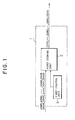
- FIG. 1 is a block diagram showing an aspect of an interleaving apparatus according to this invention.
- an interleaving apparatus 1 interleaves data to be transmitted, which has a first storing unit 2 for storing the data to be transmitted, and a first control unit 3 for controlling the first storing unit 2 to output the data to be transmitted from the first storing unit 2 with the data to be transmitted arranged in a matrix and at least either columns or rows thereof randomly rearranged.
- data to be transmitted (D000-D383) shown in FIG. 1 is merely an example.
- the first control unit 3 controls the first storing unit 2 to output the data to be transmitted from the first storing unit 2 with the data to be transmitted arranged in a matrix and at least either columns or rows thereof randomly rearranged, by using relatively easy interleaving in a simple structure, thereby preventing biased distribution of error data which leads to degradation of the transmission quality.
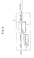
- FIG. 2 is a block diagram showing an aspect of a de-interleaving apparatus according to this invention.
- a de-interleaving apparatus 4 de-interleaves received data.
- the de-interleaving apparatus 4 has a second storing unit 5 for storing the received data, and a second control unit 6 for controlling the second storing unit 5 to output the received data in a state before the received data was interleaved from the second storing unit 5 by arranging the received data in a matrix, and randomly rearranging at least either columns or rows thereof.
- received data (D000-D383) shown in FIG. 2 is merely an example.
- the second control unit 6 controls the second storing unit 5 to output the received data in a state before interleaved from the second storing unit 5 by arranging the received data in a matrix and randomly rearranging at least either columns or rows of thereof, by using relatively easy de-interleaving in a simple structure, thereby preventing biased distribution of error data which leads to degradation of the transmission quality.
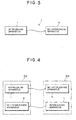
- FIG. 3 is a block diagram showing an aspect of an interleaving/de-interleaving system according to this invention.
- an interleaving/de-interleaving system 7 has an interleaving apparatus 1 for interleaving data to be transmitted, and a de-interleaving apparatus 4 for receiving the transmitted data interleaved in the interleaving apparatus 1 to de-interleave the data, wherein the interleaving apparatus 1 outputs the data to be transmitted with the data to be transmitted arranged in a matrix, and at least either columns or rows thereof randomly rearranged, and the de-interleaving apparatus 4 outputs received data in a state before the transmitted data was interleaved by arranging the received data in a matrix, and randomly rearranging at least either columns or rows thereof.
- the interleaving apparatus 1 outputs the data to be transmitted with the data to be transmitted arranged in a matrix, and at least either columns or rows thereof randomly rearranged
- the de-interleaving apparatus 4 outputs the received data in a state before the transmitted data was interleaved by arranging the received data in a matrix, and randomly rearranging at least either columns or rows thereof, thereby preventing biased distribution of data which leads to degradation of the transmission quality, relatively readily, in a simple structure even when burst errors generate in the interleaved data.
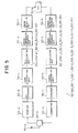
- FIG. 4 is a block diagram showing an aspect of an interleaving/de-interleaving apparatus according to this invention.
- an interleaving/de-interleaving apparatus 8A transmits/receives interleaved data to/from an opposite interleaving/de-interleaving apparatus 8B.
- the interleaving/de-interleaving apparatus 8A has an interleaving apparatus 1 for outputting data to be transmitted to the opposite interleaving/de-interleaving apparatus 8B with the data to be transmitted arranged in a matrix, and at least either columns or rows thereof randomly rearranged, and a de-interleaving apparatus 4 for outputting received data having been interleaved in the opposite interleaving/de-interleaving apparatus 8B in a state before the received data was interleaved by arranging the received data in a matrix, and randomly rearranging at least either columns or rows thereof.
- the interleaving apparatus 1 and the de-interleaving apparatus 4 randomly rearrange data to be transmitted, and randomly rearrange an array of received data, thereby preventing degradation of the transmission quality of the data to be transmitted and the received data.
- a first embodiment will be described by way of an example in which a mobile station and a base station carry out CDMA (Code Division Multiple Access) connection using a spread spectrum technique in a portable telephone system.
- CDMA Code Division Multiple Access
- FIG. 5 is a block diagram showing a structure of an MS according to the first embodiment.
- the MS 50 comprises a receiver 50-a, a de-spreader 50-b, a data extracting unit 50-c, a de-interleaving unit 50-d, an error correction decoding unit 50-e, an error detecting unit 50-f, a CPU 50-g, an error detection encoding unit 50-h, an error correction encoding unit 50-i, an interleaving unit 50-j, a signal assembling unit 50-k, a spreader 50-1, a transmitter 50-m, a duplexer 50-n and an antenna 50-p.
- the receiver 50-a modifies a signal received via the antenna 50-p and the duplexer 50-n into a signal easily processable by the de-spreader 50-1.
- the receiver 50-a not only down-converts a signal (radio frequency received signal: RF signal) received via the antenna 50-p and the duplexer 50-n into an intermediate frequency signal (IF signal) to separate the signal into I channel components and Q channel components, but also converts each of the components (I channel components and Q channel components) from analog to digital to generate a digital signal.
- RF signal radio frequency received signal
- IF signal intermediate frequency signal
- the de-spreader 50-b separates a desired signal from a digital signal sent from the receiver 50-a using a de-spreading code.
- the data extracting unit 50-c extracts data from the signal separated by the de-spreader 50-b.
- the error correction decoding unit 50-e decodes data de-interleaved by the de-interleaving unit 50-d, and corrects an error included in the data using an error correcting code. For example, an error is corrected using a parity check bit added when data (main signal) is transmitted, and the parity check bit is deleted in decoding and correcting.
- the error detecting unit 50-f detects an error detecting bit added when the data (main signal) is transmitted on the basis of a bit structure of the error detecting bit previously set. Information or data about an error or the like detected by the error detecting unit 50-f is notified the CPU 50-f.
- the error detection encoding unit 50-h encodes the error detecting bit to be used to detect an error and adds the error detecting bit to data sent from the CPU 50-g.
- the error correction encoding unit 50-i adds the error correcting code, which is to be used for error correction, to the data sent from the error detection encoding unit 50-h.
- the signal assembling unit 50-k assembles interleaved data to form a signal format suited for transmission.
- the spreader 50-l converts a signal sent from the signal assembling unit 50-k into a spread signal using a predetermined spreading code.
- the transmitter 50-m modifies a signal sent from the spreader 50-l into a signal to be transmitted.
- the transmitter 50-m converts each component (I channel or Q channel) of a digital signal sent from the spreader 50-l into an analog signal in digital/analog conversion.
- the transmitter 50-m up-converts an intermediate frequency signal (IF signal) into a radio frequency signal (RF signal) after orthogonal-modulating the signal into an orthogonal-modulated signal.
- IF signal intermediate frequency signal
- RF signal radio frequency signal
- the radio frequency signal is transmitted to the outside via the duplexer 50-n and the antenna 50-p.
- the interleaving unit (interleaving apparatus) 50-j interleaves data to be transmitted.
- the interleaving unit 50-j arranges data to be transmitted in a matrix, randomly rearranges rows and columns of the data, and outputs the rearranged data in time series.
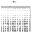
- the data (000-383) is, as shown in FIG. 6 , arranged in a matrix (16 columns by 24 rows), after that, columns of the data are rearranged, as shown in FIG. 7 .
- the columns (A to P) are arranged in alphabetical order, but the data is rearranged in the order of A, P, J, ... and so on by rearranging the columns of the data, as shown in FIG. 7 .
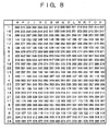
- the rows of the data (000-383) are rearranged, as shown in FIG. 8 .
- the rows (1-24) are arranged in the order numbered, but the rows are rearranged in the order of 1, 16, 19, 10, 17, ... and so on by the rearranging the rows, as shown in FIG. 8 .
- the data arranged in a matrix as shown in FIG. 8 is read out in order column by column, beginning with "000" in column A, whereby the order in which the data has been arranged is randomly rearranged. Namely, the read data is irregularly rearranged, as shown in FIG. 9 .
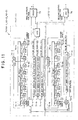
- FIG. 10 is a block diagram showing the interleaving apparatus 50-j according to the first embodiment of this invention.
- the interleaving apparatus 50-j comprises an interleaving RAM (Random Access Memory) 51 and a control processing unit 52.
- RAM Random Access Memory
- the interleaving RAM (first storing unit) (hereinafter referred as "first RAM 51") stores data to be transmitted.
- the control processing unit (first control unit) 52 controls the first RAM 51 so that the data to be transmitted is transmitted from the first RAM 51 with the data to be transmitted arranged in a matrix and rows or columns thereof randomly rearranged.
- the first control processing unit 52 comprises a write processing unit 60 (hereinafter referred as “first write processing unit”) and a read processing unit 70 (hereinafter referred as “first read processing unit 70).
- the first write processing unit 60 performs a control to write data in the first RAM 51, which outputs an address and an enable signal (not shown).
- the first writing processing unit 60 writes signals sent from the error correction encoding unit 50-i in order of addresses.
- the first write processing unit 60 comprises a counter 61, as shown in FIG. 10 .
- the counter 61 generates count values from “0" to "383".
- the counter 61 counts up the value in ascending order, and again counts from "0" when the count value reaches the maximum value.
- Each of the count values (0-383) is used as an address for input data.
- the first data "000", for example, is stored in the 0th address with a count value "0" outputted from the counter 61 as an address.
- the 107th data is stored in the 106th address with a count value "106" as an address.
- the read processing unit (first read processing unit) 70 generates an address used to read the data to be transmitted from the first RAM 51 with the data to be transmitted stored in the first RAM 51 arranged in a matrix and columns and rows thereof randomly rearranged, so as to read the data.
- the first read processing unit 70 reads the data (refer to FIG. 6 ) having been arranged in a matrix and held in the first RAM 51 from the first RAM 51 in a data array shown in FIG. 9 .
- the first read processing unit 70 comprises an A column generating circuit 71, a one row generating circuit 72 and an adder 73.
- the A column generating circuit (column number generating unit) 71 randomly generates a column number, which generates any one of 24 numbers (a multiplex of 16 or 000 among 000-383) in column A shown in FIG. 8 .
- the A column generating circuit 71 generates 24 numbers in column A within one cycle , then is reset when completing generation of 24 numbers and shifting to the next cycle, and again outputs 24 numbers in column A. Additionally, the A column generating circuit 71 outputs a carry pulse to the one row generating unit 72 when the cycle is changed.
- the one row generating unit (row number generating unit) 72 generates a row number, which generates any one of 16 numbers (000-015) in one row shown in FIG. 8 .
- the one row generating unit 72 randomly changes row numbers to be outputted each time all 24 column numbers in column A are outputted (in each cycle of the A column generating circuit 71).
- the one row generating circuit 72 is reset, thereby again outputting 16 numbers in one row.
- the adder 73 outputs a value obtained by adding numbers outputted from the A column generating circuit 71 and the one row generating circuit 72 as a read address for the first RAM 51.
- Table 1 below shows an example of data outputted from the A column generating circuit 71, the one row generating circuit 72 and the adder 73.
- Table 1 Example of output data t1 t2 t3 ... t22 t23 t24 t25 t26 t27 ... t46 t47 output of A column generating circuit 000 240 288 ... 112 304 368 000 240 288 ... 112 304 Output of one row generating circuit 000 000 000 000 ... 000 000 000 000 015 015 015 ... 015 015 Output of adder 000 240 288 ... 112 304 368 015 255 303 ... 127 319
- the A column generating circuit 71 outputs a different column number at each timing, whereas the one row generating circuit 72 outputs the same row number.
- the one row generating circuit 72 outputs the next number. While numbers sent from the A column generating circuit 71 are taking a round (one cycle), the same number is outputted from the one row generating circuit 72. Only after numbers for 24 cycles are outputted from the A column generating circuit 71, the one row generating circuit 72 completes outputting of numbers (16 numbers from 000 to 015) for one cycle.
- the A column generating circuit 71 outputs 24 numbers in a cycle, whereas the one row generating circuit 72 outputs the same number in the same cycle, and outputs a different number each time the cycle is changed.
- a value (read address) outputted from the adder 73 is a sum of "240" outputted from the A column generating circuit 71 and "015" outputted from the one row generating circuit 72.
- FIG. 11 is a diagram showing a detailed structure of the first read processing unit 70 according to the first embodiment of this invention.
- the first read processing unit 70 shown in FIG. 11 comprises the A column generating circuit 71, the one row generating circuit 72, the adder 73 and an AND circuit 74.
- the A column generating circuit 71 comprises, as shown in FIG. 11 , an EX-OR (exclusive OR) circuit (hereinafter referred merely as "EX-OR") 75-a, a shift register 75-b, a setting control unit 75-c, a first selecting circuit 71-a, a second selecting circuit 71-b, a third selecting circuit 71-c and an AND circuit 71-d.
- EX-OR exclusive OR
- the A column generating circuit 71 generates 24 numbers (refer to FIG. 8 ) in column A using data of 9 bits.
- the shift register 75-b holds data of 9 bits, which comprises flip-flops (hereinafter referred as "FF") 75-bl through 75-b9.
- FF flip-flops
- the FFs 75-bl through 75-b9 each holds a bit of "1 (High)" when activated under a control of the setting control unit 75-c performing a control when the apparatus is activated.
- Data held in the shift register 75-b is successively shifted according to a clock (CLK). Bits outputted from the FF 75-b9 and the FF 75-b6 undergo an exclusive-OR operation in the EX-OR 75-a, then a resulting bit is held as a lower bit in the FF 75-b1.
- Table 2 below shows an example of transition of a bit structure held in the shift register 75-b.
- the first to third selecting circuits 71-a through 71-c and the AND circuit 71-d monitor data of 9 bits outputted from the A column generating circuit 71.
- the first selecting circuit 71-a determines whether or not a numerical value represented by data (binary number) of 9 bits corresponds to a multiple of 16 and 0 as decimal numbers. In concrete, the first selecting circuit 71-a determines whether or not lower 4 bits among 9 bits are all "0". When the lower 4 bits are all "0", the first selecting circuit 71-a outputs a pulse (described as "pulse when YES" in FIG. 11 ).
- the second selecting circuit 71-b determines whether or not a numerical value represented by data (binary number) of 9 bits is any numerical value among 0 to 368 as decimal numbers.
- the third selecting circuit 71-b determines whether or not the 9 bits are all "1 (High)". When the 9 bits are all "1", the third selecting circuit 71-b outputs a pulse (carry pulse) (described as "pulse when YES” in FIG. 11 ).
- the one row generating circuit 72 shown in FIG. 11 comprises, similarly to the A column generating circuit 71, an EX-OR 75-a, a shift register 75-b and a setting control unit 75-c.
- the one row generating circuit 72 comprises a fourth selecting circuit 72-a and a switch (SW) 72-b.
- the switch 72-b performs a control to send a clock (CLK) signal to the shift register 75-b according to a pulse outputted from the third selecting circuit 71-c or the fourth selecting circuit 72-a.
- CLK clock
- the switch 72-b sends a clock signal to the shift register 75-b (ON control).
- the switch 72-b prevents a clock signal from passing therethrough (OFF control).
- the fourth selecting circuit 72-a determines whether or not a numerical value represented by data (binary number) of 9 bits corresponds to any one of 0 to 15 as decimal numbers. In concrete, the fourth selecting circuit 72-a determines whether or not bits higher than lower 5 bits among the 9 bits include "1". When the bits higher than the lower 5 bits do not include "1", the fourth selecting circuit 72-a outputs a pulse signal (described as "pulse when YES" in FIG. 11 ).
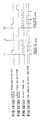
- FIGS. 12(a) through 12(d) are time charts for illustrating a schematic operation of the shift register 75-b in the one row generating circuit 72.
- FIG. 12(a) shows a timing at which a pulse signal is outputted from the third selecting circuit 71-c.
- FIG. 12(b) shows a timing at which a pulse signal is outputted from the fourth selecting circuit 72-a.
- FIG. 12(c) shows a timing at which a clock signal is outputted from the switch 72-b.
- FIG. 12(d) is a time chart showing transition timings for data held in the shift register 75-b.
- the switch 72-b sends a clock signal to the shift register 75-b in ON control [refer to FIG. 12(c) ].
- the shift register 75-b shifts the data to change the data structure of 9 bits held therein [described as "points of change of data" in FIG. 12(d) ].
- the switch 72-b when a pulse signal is outputted from the fourth selecting circuit 72-a at a timing T2, the switch 72-b changes its state from where the switch 72-b sends a clock signal before the timing T2 to where the switch 72-b does not send a clock signal to the shift register 75-b [refer to FIG. 12(c) ], so that the shift register 75-b does not shift the data but keeps the preceding state (does not change the data).
- the shift register 75-b shifts the data to change the bit structure in a similar way to the above.
- the AND circuit shown in FIG. 11 performs a control to output an enable signal to be used to read data stored in an address outputted from the adder 73.
- the AND circuit 74 outputs an enable signal.
- the first selecting circuit 71-a and the second selecting circuits 71-b output pulse signals to the AND circuit 71-d, and the AND circuit 71-d outputs a pulse signal to the AND circuit 74.
- the fourth selecting circuit 72-a When a value sent from the one row generating circuit 72 to the adder 73 corresponds to any one of "0 to 15 (decimal numbers)", the fourth selecting circuit 72-a outputs a pulse signal to the AND circuit 74.
- the AND circuit 74 outputs an enable signal to the first RAM 51 when receiving pulse signals from the AND circuit 71-d and the fourth selecting circuit 72-a.
- the A column generating circuit 71 and the one row generating circuit 72 shown in FIG. 10 are reset. However, in the structure shown in FIG. 11 , the A column generating circuit 71 and the one row generating circuit 72 are not reset every cycle. Namely, the bit structure of the shift register 75-b becomes all "1" when a predetermined time is elapsed.
- the de-interleaving unit (de-interleaving apparatus) 50-d shown in FIG. 5 de-interleaves received data.
- the de-interleaving unit 50-d arranges received data having been interleaved in a matrix, randomly rearranges at least either columns or rows of the data, and outputs the data in time series, thereby outputting the received data in the order before the received data was interleaved.
- the received data (000-383) is rearranged in the order before the received data was interleaved.
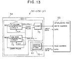
- FIG. 13 is a block diagram showing the de-interleaving apparatus 50-d according to the first embodiment of this invention.
- the de-interleaving apparatus 50-d comprises an interleaving RAM 53 and a control processing unit 54.
- the interleaving RAM (second storing unit) 53 (hereinafter referred as "second RAM 53") stores received data.
- the control processing unit (second control unit) 54 (hereinafter referred as "second control processing unit 54") controls the second RAM 53 so that the received data is outputted from the second RAM 53 in a state before the received data was interleaved by arranging the received data in a matrix and randomly rearranging columns and rows thereof.
- the second control processing unit 54 comprises a write processing unit 60-1 (hereinafter referred as “second write processing unit 60-1”) and a read processing unit (hereinafter referred as “second read processing unit 70-1").
- the write processing unit (second write processing unit) 60-1 generates an address used to write the received data in the second RAM 53 in a state before the received data was interleaved by arranging the received data in a matrix and randomly rearranging columns and rows thereof, thereby writing the received data.
- the write processing unit 60-1 performs a data writing control so that received data having been interleaved (refer to FIG. 9 ) is stored in the second RAM 53 in a state of the matrix shown in FIG. 6 by rearranging columns and rows thereof.
- the second write processing unit 60-1 comprises, as shown in FIG. 13 , an A column generating circuit 71, a one row generating circuit 72 and an adder 73.
- the second write processing unit 60-1 comprising the A column generating circuit 71, the one row generating circuit and the adder 73 may, as shown in FIG. 11 , also comprises an EX-OR 75-a, a shift register 75-b, a setting control unit 75-c, a first selecting circuit 71-a, a second selecting circuit 71-b, a third selecting circuit 71-c, an AND circuit 71-d, a fourth selecting circuit 72-a and a switch (SW) 72-b, similarly to the above read processing unit 70.
- a number outputted from the adder 73 shown in FIG. 13 is used as a write address, as shown in FIG. 13 .
- the second read processing unit 70-1 shown in FIG. 13 reads data from the second RAM 53, outputs an address and an enable signal (not shown), and comprises a counter 61, as shown in FIG. 13 .
- Data read out from the second RAM 53 on the basis of a count value "0-383" which is sent from the counter 61 in the second read processing unit 70-1 is read out in numerical order as "000”, "001", “002", “003”, ..., "150”, ..., 250", ..., "382" and "383".
- the MS 50 comprises the interleaving unit 50-j and the de-interleaving unit 50-d, the MS 50 has a function as an interleaving/de-interleaving apparatus which transmits/receives interleaved data to/from an opposite interleaving/de-interleaving apparatus.
- the BS performing CDMA communication with the MS 50 transmits/receives data to/from the MS 50.
- the BS 100 comprises, as shown in FIG. 5 , a receiver 50-a, a de-spreader 50-b, a data extracting unit 50-c, a de-interleaving unit (de-interleaving apparatus) 50-d, an error correction decoding unit 50-e, an error detecting unit 50-f, a CPU 50-g, an error detection encoding unit 50-h, an error correction encoding unit 50-i, an interleaving unit (interleaving apparatus) 50-j, a signal assembling unit 50-k, a spreader 50-l, a transmitter 50-m, a duplexer 50-n and an antenna 50-p, similarly to the foregoing MS 50.
- the BS 100 may be provided with the de-spreader 50-b and the spreader 50-l for each spreading code. Additionally, in order to process received data and data to be transmitted for each spreading code, the BS 100 may be provided with the data extracting unit 50-c, the de-interleaving unit 50-d, the error correction decoding unit 50-e, the error detecting unit 50-f, the error detection encoding unit 50-h, the error correction encoding unit 50-j, the interleaving unit 50-h and the signal assembling unit 50-k.
- the MS 50 when the MS 50 transmits data to the BS 100, the MS 50 randomly rearranges columns and rows of data to which an error correcting code is added in the error correction encoding unit 50-i by the interleaving unit 50-j, and outputs the data in a state as shown in FIG. 9 to the signal assembling unit 50-k.
- the interleaved data is assembled into a predetermined transmit data length by the signal assembling unit 50-k, then spread using a predetermined spreading code by the spreader 50-1.
- the spread interleaved data (digital signal) is converted or the like into an RF signal by the transmitter 50-m, then transmitted to the outside via the duplexer 50-n and the antenna 50-p.
- the receiver 50-a converts or the like the RF signal into a digital signal
- the de-spreader 50-b de-spreads the signal using a predetermined de-spreading code.
- the data extracting unit 50-c extracts data having been interleaved by the interleaving unit 50-j in the MS 50, and the de-interleaving unit 50-d randomly rearranges columns and rows of the interleaved data to arrange the data in the order of before the interleaved data was interleaved, and sends the data to the error correction decoding unit 50-e.
- the error correction decoding unit 50-e corrects a correctable error using an error correction code, and notifies of information on the error detected by the error detecting unit 50-f the CPU 50-g.
- a processing on data to be transmitted from the BS 100 to the MS 50 is similar to the above, detailed description of which is omitted here.
- the MS 50 on the transmitting side rearranges the data using relatively easy interleaving in a simple structure when transmitting the data so that distribution of the data is not biased, and transmits the data
- the BS 100 on the receiving side makes distribution of the error data be without bias using relatively easy de-interleaving in a simple structure when receiving the interleaved data, thereby preventing degradation of the transmission quality.
- An MS 50-1 and a BS 100-1 according to the first modification of the first embodiment has similar functions to the MS 50 and the BS 100 according to the first embodiment.
- a de-interleaving unit according to the first modification of the first embodiment randomly generates an address used to read the data.
- FIG. 14 is a diagram showing a structure of a de-interleaving unit 50-d1 according to the first modification of the first embodiment of this invention.
- the de-interleaving unit 50-dl comprises a second RAM 53-1 and a control processing unit 54-1.
- the second RAM 53-1 stores received data, similarly to the second RAM 53.
- the control processing unit (second control unit) 54-1 performs a control on the second RAM 53-1 so that received data is outputted from the second RAM 53-1 in a state before the received data was interleaved by arranging the received data in a matrix and randomly rearranging columns and rows thereof, in a similar way to the second control processing unit 54 according to the first embodiment.
- control processing unit 54-1 comprises, as shown in FIG. 14 , a write processing unit 60-2 (hereinafter referred as “third write processing unit 60-2”) and a read processing unit 70-2 (hereinafter referred as “third read processing unit 70-2").
- the third write processing unit 60-2 has a similar function to the first write processing unit 60 according to the first embodiment, which performs a control to write data in the second RAM 53-1, and outputs an address and an enable signal (not shown).
- the third write processing unit 60-2 comprises a counter 61.
- the third read processing unit (second read processing unit) 70-2 generates a read address used to read the received data from the second RAM 53-1 in a state before the received data was interleaved by arranging the received data written in the second RAM 53-1 in a matrix and randomly rearranging columns and rows thereof.
- the third read processing unit 70-2 comprises an A column generating circuit 71-1, a one row generating circuit 72-1 and an adder 73.
- the A column generating circuit 71-1 has a similar function to the A column generating circuit 71 according to the first embodiment, the A column generating circuit 71-1 generates numbers different from those generated by the A column generating circuit 71.
- the A column generating circuit 71-1 In concrete, as contrasted with the A column generating circuit 71 generating 24 numbers, the A column generating circuit 71-1 generates 16 numbers. However, the numbers generated by the A column generating circuit 71 and the numbers generated by the A column generated circuit 71-1 are different from each other. The numbers generated by the A column generating circuit 71-1 are "000”, “144”, “120”, “216”, “096”, “312”, “192”, “360”, “072”, “048”, “288”, "240”, “168", "264”, “336” and "024", when described in the order generated.
- the one row generating circuit 72-1 has a similar function to the one row generating circuit 72 according to the first embodiment, numbers generated by the one row generating circuit 72-1 are different from those generated by the one row generating circuit 72.
- the one row generating circuit 72 generates 16 numbers
- the one row generating circuit 72-1 generates 24 numbers.
- numbers generated by the one row generating circuit 72 and the one row generating circuit 72-1 are different from each other.
- the numbers generated by the one row generating circuit 72-1 are "000”, “008", “007”, “013”, “006”, “019”, “012”, “021”, “005", “003”, “018”, “015", "011”, “016”, “020”, “010”, “004", “009”, "002", “022”, “017”, “010”, “014" and “023”, when described in the order generated.
- FIG. 15 is a diagram showing values outputted from the A column generating circuit 71-1, the one row generating circuit 72-1 and the adder 73. As shown in FIG. 15 , a value obtained by adding values outputted from the A column generating circuit 71-1 and the one row generating circuit 72-1 is outputted from the adder 73, and used as a read address.
- the one row generating circuit 72-1 When 16 numbers are completed to be outputted from the A column generating circuit 71-1, the one row generating circuit 72-1 outputs a different number, as shown in FIG. 15 .
- Broken line ⁇ shown in FIG. 15 shows a change of the data outputted from the one row generating circuit 72-1.
- the A column generating circuit 71-1 and the one row generating circuit 72-1 according to the first modification may be configured in a similar way to the A column generating circuit 71 and the one row generating circuit 72 shown in FIG. 11 , respectively.
- the first selecting circuit 71-a selects a multiple of "24”
- the fourth selecting circuit 72-a outputs a pulse signal when the value falls within "0-23”.
- data interleaved in the MS 50-1 is rearranged in the order before the interleaved data was interleaved by the de-interleaving unit 50-d1 in the BS 100-1.
- the MS 50-1 and the BS 100-1 according to the first embodiment of this invention, even if data transmitted from the MS 50-1 to the BS 100-1 is affected by fading that errors are generated in the transmitted data, for example, the MS 50-1 on the transmitting side having a simple structure rearranges the data using relatively easy interleaving so that distribution of the errors is not biased, while the BS 100-1 on the receiving side having a simple structure makes the distribution of the errors of the data be not biased when receiving the interleaved data, thereby preventing degradation of the transmission quality.
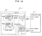
- the interleaving unit 50-j randomly generating a read address to be used to read data from the first RAM 51 in interleaving with an interleaving unit 50-j1 as shown in FIG. 16 randomly generating a write address used to write data in the first RAM 51-1.
- the interleaved data is de-interleaved using the de-interleaving unit 50-d according to the first embodiment.
- the interleaving unit 15-1 comprises, as shown in FIG. 16 , a first RAM 51-1 and a control processing unit 52-1.
- the first RAM 51-1 stores data to be transmitted, similarly to the first RAM 51.
- the control processing unit 52-1 performs a control on the first RAM 51-1 so that data to be transmitted is outputted from the first RAM 51-1 with the data to be transmitted arranged in a matrix and columns and rows thereof randomly rearranged, in a similar manner to the first control processing unit 52 according to the first embodiment.
- control processing unit 52-1 comprises, as shown in FIG. 16 , a write processing unit 60-3 (hereinafter referred as “fourth write processing unit 60-3”) and a read processing unit 70-3 (hereinafter referred as “fourth read processing unit 70-3).
- the fourth read processing unit 70-3 functions in a similar manner to the second read processing unit 60-2 according to the first embodiment.
- the fourth read processing unit 70-3 performs a control to read data from the first RAM 51-1, and comprises a counter 61.
- the fourth write processing unit (first write control unit) 60-3 performs a control on the first RAM 51-1 so that data to be transmitted is outputted from the first RAM 51-1 with the data to be transmitted arranged in a matrix and columns and rows thereof randomly rearranged.
- the fourth write processing unit 60-3 comprises an A column generating circuit 71-1, a one row generating circuit 72-1 and an adder 73.
- the A column generating circuit 71-1 and the one row generating circuit 72-1 of the interleaving unit 50-j1 may be configured in a similar way to the A column generating circuit 71 and the one row generating circuit 72 shown in FIG. 11 , respectively.
- the first selecting circuit 71-a selects a multiple of "24”
- the fourth selecting circuit 72-a outputs a pulse signal when the value falls within "0-23".
- the de-interleaving unit 50-d randomly rearranges columns and rows of data interleaved by the interleaving unit 50-jl, and reads the data in the order before the interleaved data was interleaved.
- a combination of the interleaving unit 50-jl and the de-interleaving unit 50-d can readily prevent degradation of the transmission quality as well even if burst errors generate during transmission.
- An MS 50-2 and a BS 100-2 according to the second modification of the first embodiment have similar functions to the MS 50 and the BS 100 according to the first embodiment, respectively.
- the structure of the interleaving unit 50-j according to the first embodiment shown in FIG. 10 and the structure of the de-interleaving unit 50-d according to the first embodiment shown in FIG. 13 are exchanged to each other to form an interleaving unit 50-j2 and a de-interleaving unit 50-d2.
- the de-interleaving unit 50-d2 is configured in a similar manner to the interleaving unit 50-j, as shown in FIG. 10 .
- the first RAM 51 shown in FIG. 10 stores input data sent from the data extracting unit 50-c, and outputs the data held therein to the error correction decoding unit 50-e under a control of the first read processing unit 70.
- the interleaving unit 50-j2 is configured in a similar manner to the de-interleaving unit 50-d, as shown in FIG. 13 .
- the second RAM 53 shown in FIG. 13 stores input data sent from the error correction encoding unit 50-i under a control of the second write processing unit 60-1, and outputs the data held therein to the signal assembling unit 50-k under a control of the second read processing unit 70-1.
- the MS 50-2 on the transmitting side randomly rearranges columns and rows of the data to be transmitted when transmitting
- the BS 100-2 on the receiving side rearranges the data in the order before the interleaved data was interleaved when receiving the interleaved data, in a similar way to the MS 50 and the BS 100 according to the first embodiment.
- the receiving side reforms the data into a readily correctable form to randomly distribute the errors, thereby readily correcting the errors, which prevents degradation of the transmission quality.
- the above is the same even when the structures of the de-interleaving unit 50-d1 and the interleaving unit 50-j according to the first modification of the first embodiment are exchanged, or structures of the interleaving unit 50-j1 and the de-interleaving unit 50-d are exchanged.
- An MS 50-3 and a BS 100-3 shown in FIG. 5 according to the second embodiment have similar functions to the MS 50 and the BS 100 according to the first embodiment, respectively.
- the BS 50-3 and the BS 100-3 are different from those according to the first embodiment in a point that each of the A column generating circuit 71 and the one row generating circuit 72 in the de-interleaving unit 50-d and the interleaving unit 50-j according to the first embodiment is configured with a ROM and a counter.
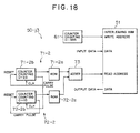
- FIG. 17 is a block diagram showing a de-interleaving unit according to the second embodiment.
- a de-interleaving unit 50-d3 comprises an A column generating circuit 71-2 and a one row generating circuit 72-2 along with a second RAM 53, an adder 73 and a counter 61, similar to those of the de-interleaving unit 50-d according to the first embodiment.
- the A column generating circuit 71-2 comprises a similar function to the A column generating circuit 71 according to the first embodiment, but has a ROM (Read Only Memory) 71-2a and a counter 71-2b, as shown in FIG. 17 .
- the ROM (memory) 71-2a holds 24 numbers (refer to FIG. 8 ) in the A column in predetermined addresses, respectively.
- Table 3 below shows an example of data held in the ROM 71-2a. [table 3] Example of held data Address 0 1 2 3 4 5 6 7 ... 20 21 22 23 Data 000 240 288 144 256 128 064 032 ... 224 112 304 368
- the ROM 71-2a holds 24 numbers in column A shown in FIG. 8 in the descending order. For example, a number "256" is held in an address "4".
- the ROM 71-2a receives a count value (address in Table 3 above) outputted from the counter 71-2b, the ROM 71-2a reads data held in that address, and outputs the data to the adder 73.
- the counter 71-2b is a free-running counter, which counts from “0” to "23", outputs a count value as a read address for the ROM 71-2a, and again counts from "0" when the count value reaches a maximum count value "23".
- the counter 71-2b sends a carry pulse to the counter 72-2b (to be described later) when a count cycle takes a round.
- the one row generating circuit 72-2 has a similar function to the one row generating circuit 72 according to the first embodiment, but comprises a ROM 72-2a and a counter 72-2b, as shown in FIG. 17 .
- the ROM (memory) 72-2a holds 16 numbers (refer to FIG. 8 ) in one row at predetermined addresses, respectively.
- Table 4 below shows an example of data held in the ROM 72-2a. [table 4] Example of held data Address 0 1 2 3 4 5 6 7 ... 12 13 14 15 data 000 015 009 008 004 002 001 012 ... 010 005 014 007
- the ROM 72-2a holds 16 number in one row shown in FIG. 8 in order, from left to right. For example, a number "008" is held in an address "3".
- the ROM 72-2a receives a count value (address in Table 4 above) outputted from the counter 72-2b, the ROM 72-2a reads data held in that address and outputs the data to the adder 73.
- the counter 72-2b counts from “0” to “15”, outputting a count value as a read address for the ROM 72-2a and again counting from “0" when the count value reaches a maximum count value "15".
- the counter 72-2b counts up by receiving a carry pulse from the counter 71-2b in the A column generating circuit 71-2.
- FIG. 18 is a block diagram showing an interleaving unit according to the second embodiment.
- an interleaving unit 50-j3 comprises an A column generating circuit 71-2 and a one row generating circuit 72-2 along with a first RAM 51, an adder 73 and a counter 61 similar to those of the interleaving unit 50-j according to the first embodiment.
- the interleaving unit 50-j3 of the MS 50 randomly shuffles columns and rows of the data to be transmitted, and sends the interleaved data in the order as shown in FIG. 9 to the signal assembling unit 50-k, in a similar manner to the MS 50 and the BS 100 according to the first embodiment.
- the interleaving unit 50-j3 reads data stored in the first RAM 51 using a value obtained by adding data (refer to foregoing Tables 3 and 4) sent from ROM 71-2a and the ROM 72-2a by the adder 73 as a read address to randomly read 384 of data (000-383).
- the interleaved data is sent to the BS 100-3 via the spreader 50-1, etc.
- the BS 100-3 receives the data sent from the MS 50-1 via the de-spreader 50-b, etc., de-interleaves the data by the de-interleaving unit 50-d3, and sends the data in the order before the interleaved data was interleaved to the error correction decoding unit 50-e.
- the de-interleaving unit 50-d3 reads data stored in the second RAM 53 using a value obtained by adding data (refer to foregoing Tables 3 and 4) sent from the ROM 71-2a and the ROM 72-2a as a write address to randomly write 384 of data in the second RAM 53. After writing the data in the second RAM 53, the de-interleaving unit 50-d3 performs a control to read the 384 of data in order, beginning with a count value "0" of the counter 61.
- An MS 50-4 and a BS 100-4 according to the modification of the second embodiment shown in FIG. 5 have similar functions to the MS 50-3 and the BS 100-3 according to the second embodiment, respectively, but are different from those according to the second embodiment in a point that a ROM is used to randomly generate an address when data is interleaved or de-interleaved, unlike the de-interleaving unit 50-d3 and the interleaving unit 50-j3 according to the second embodiment.
- Each of the MS 50-4 and the BS 100-4 comprises a de-interleaving apparatus 50-d1 according to the first modification of the first embodiment in lieu of the de-interleaving unit 50-d3 according to the second embodiment.
- ROMs 71-2a and 72-2a in random generation facilitates easy setting of an order or the like in which 24 numbers in column A and 16 numbers in one row are to be generated, which becomes a reference for address generation, thereby certainly rearranging 384 of data (000-383), which leads to prevention against degradation of the transmission quality.
- Each of the MS 50-4 and the BS 100-4 may be provided with the interleaving apparatus 50-j1 according to the first modification of the first embodiment in lieu of the interleaving unit 50-j3 according to the second embodiment. In such case, it is possible to prevent degradation of the transmission quality, as well.
- the random generation on the receiving side can be readily realized using the ROMs 71-2a and 72-2a.
- the interleaving unit 50-j interleaves data to which an error correcting code is added in the error correction encoding unit 50-i.
- the error correction encoding unit 50-i may have a function of interleaving when a turbo code is used as the error correcting code.
- a turbo code is a code in combination of a convolution code, a BCH code, a Reed-Solomon code and interleaving.
- FIG. 19 is a diagram showing an error correction encoding unit 50-i1 having an interleaving function.
- the error correction encoding unit 50-i1 shown in FIG. 19 comprises an interleaving unit 50-j and encoding apparatus 50-ia.
- the encoding apparatus 50-ia (designated as "ENC” in the drawing) performs convolution or the like.
- the data u When data u is inputted to the error correction encoding unit 50-i1 shown in FIG. 19 , the data u is formed into three signals X a , X b , and X c through the encoding apparatus 50-ia, the interleaving unit 50-j, etc.
- the data X a , X b , and X c are sent to the interleaving unit 50-j, interleaved, respectively, and transmitted to the outside via the spreader 50-1, etc.
- data y a , y b , and y c on the receiving side (assuming that X a , X b , and X c are modified into y a , y b , and y c , respectively, by an effect of fading during transmission) is sent to the error correction decoding unit 50-e1 shown in FIG. 20 .
- the error correction decoding unit 50-e1. comprises, as shown in FIG. 20 , decoding apparatus 50-ea, an interleaving unit 50-j and a de-interleaving unit 50-d.
- the decoding apparatus 50-ea performs convolution decoding and the like.
- the interleaving unit 50-j interleaves data y a ' obtained by decoding the data y a and y b .
- Data y a " obtained by decoding the interleaved data and the data y c is further de-interleaved.
- the error correction decoding unit 50-e1 performs a processing similar to decoding or the like with the data de-interleaved by the de-interleaving unit 50-d and the data y b , and outputs decoded data u' whose correlation has been decreased.
- FIG. 21 is a block diagram showing an interleaving unit 50-j5.
- the interleaving unit 50-j5 comprises interleaving RAMS 56A through 56C, counters 61A through 61C, adders 73 through 75, row generating circuits 71A, 72B and 72C, and column generating circuits 72A, 71B and 71C.
- Each of the interleaving RAMs (first storing unit) 56A through 56C is similar to the first RAM 51, which stores data to be transmitted.
- Each of the row generating circuit 71A and the column generating circuits 71B and 71C has a similar function to the A column generating circuit, which outputs a different number at each timing to the adder.
- the row generating unit 71A outputs 16 numbers in one row shown in FIG. 7 .
- the column generating circuit 71B generates numbers (000-015) in order, beginning with "000”.
- the column generating circuit 71C generates "000” and multiples of 16 among numbers (000-368) in order, beginning with "000” up to "368".
- Each of the column generating circuit 72A and the row generating circuits 72B and 72C has a similar function to the one row generating circuit 72.
- the column generating circuit 72A generates numbers (000-015) in order, beginning with "000”.
- the row generating circuit 72B generates 24 numbers in column A shown in FIG. 8 in the descending order.
- the row generating circuit 72C generates numbers (000-015) in order, beginning with "000".
- Each of the column generating circuit 72A and the row generating circuits 72B and 72C varies a number to be outputted to the adder 73 with reception of a carry pulse from the corresponding row generating circuit 71A, the column generating circuit 71B or 71C as an opportunity.
- the interleaving apparatus 50-j5 shown in FIG. 21 rearranges the data (000-383) as shown in FIGS. 6 through 8 , so that the data is arranged in the order shown in FIG. 9 .
- FIGS. 25 through 32 are diagrams for illustrating interleaving (24[4[2 ⁇ 2] ⁇ 6[3 ⁇ 2]] ⁇ 16[4[[2 ⁇ 2] ⁇ 4[2 ⁇ 2]]).
- interleaving 24[4[2 ⁇ 2] ⁇ 6[3 ⁇ 2]] ⁇ 16[4[[2 ⁇ 2] ⁇ 4[2 ⁇ 2]]
- 384 of data are arranged in a matrix of 24 rows by 16 columns as shown in FIG. 25 .
- FIG. 26 is a diagram showing a state where the 384 of data are arranged after the columns thereof shown in FIG. 25 are rearranged.
- FIG. 27 is a diagram showing a state where the 384 of data whose columns shown in FIG. 26 have been rearranged.
- FIG. 28 is a diagram showing a state in which the 384 of data whose columns have been rearranged are arranged.
- FIG. 29 is a diagram showing a state where the 384 of data are arranged after the rows thereof have been rearranged.
- FIG. 30 is a diagram showing a state where the 384 of data whose rows shown in FIG. 29 have been rearranged are arranged.
- FIG. 31 is a diagram showing a state where the 384 of data whose rows shown in FIG. 30 have been rearranged are arranged.
- the 384 of data are read out in the direction of column as "'000”, "192”, “096”, “288”, “032", "224” "128” and so on.
- the data are again read out in the direction of row, beginning with the head of the column on the right.
- FIG. 32 is a diagram showing a state where interleaved 368 of data are arranged.
- the interleaved 368 of data shown in FIG. 32 are arranged, beginning with “000", in a direction from left to right, the data "368" shown at the right end is followed by “008", “376” is followed by "004", and so on.
- the above interleaving (24[4[2 ⁇ 2] ⁇ 6[3 ⁇ 2]] ⁇ 16[4[[2 ⁇ 2] ⁇ 4[2 ⁇ 2]]) can be readily carried out using the above A column generating circuit 71 or the like, and the above one row generating circuit 72 or the like.
- the A column generating circuit 71 or the like is so configured as to generate 24 numbers ("000”, “192”, “096”, “288”, “032”, “224”, “128”, “320”, “064", "256", “160”, “352”, “016”, “208”, “112”, “304”, “048”, “240”, “144”, “336”, “080”, “272", “176” and “386” in the order generated) in column A' shown in FIG. 31 .
- the one row generating circuit 72 or the like is so configured as to generate 16 numbers ("000”, “008”, “004", “012”, “002”, “010”, “006”, “014", "001", “009”, “005", “013", “003”, “011”, “007” and “015" in the order generated) in row 1' shown in FIG. 31 .
- the present invention can perform not only the above interleaving (24[4[2 ⁇ 2] ⁇ 6[3 ⁇ 2]] ⁇ 16[4[[2 ⁇ 2] ⁇ 4[2 ⁇ 2]]), but also (20[4[2 ⁇ 2] ⁇ 5[3 ⁇ 2]] ⁇ 16[4[[2 ⁇ 2] ⁇ 4[2 ⁇ 2]]) or the like.
Landscapes
- Engineering & Computer Science (AREA)
- Physics & Mathematics (AREA)
- Probability & Statistics with Applications (AREA)
- Theoretical Computer Science (AREA)
- Computing Systems (AREA)
- Detection And Prevention Of Errors In Transmission (AREA)
- Error Detection And Correction (AREA)
Applications Claiming Priority (2)
| Application Number | Priority Date | Filing Date | Title |
|---|---|---|---|
| JP31151298A JP3257984B2 (ja) | 1998-10-30 | 1998-10-30 | インタリーブ方法及びデインタリーブ方法並びにインタリーブ装置及びデインタリーブ装置並びにインタリーブ/デインタリーブシステム並びにインタリーブ/デインタリーブ装置並びにインタリーブ機能付きの送信装置,デインタリーブ機能付きの受信装置及びインタリーブ/デインタリーブ機能付きの送受信装置 |
| EP99108558A EP0998046B1 (de) | 1998-10-30 | 1999-05-05 | Verschachtelungsverfahren und Vorrichtung, Entschachtelungsverfahren und Vorrichtung sowie Verschachtelungs/Entschachtelungssystem und Vorrichtung |
Related Parent Applications (1)
| Application Number | Title | Priority Date | Filing Date |
|---|---|---|---|
| EP99108558.0 Division | 1999-05-05 |
Publications (2)
| Publication Number | Publication Date |
|---|---|
| EP2267904A2 true EP2267904A2 (de) | 2010-12-29 |
| EP2267904A3 EP2267904A3 (de) | 2011-02-16 |
Family
ID=18018135
Family Applications (2)
| Application Number | Title | Priority Date | Filing Date |
|---|---|---|---|
| EP99108558A Expired - Lifetime EP0998046B1 (de) | 1998-10-30 | 1999-05-05 | Verschachtelungsverfahren und Vorrichtung, Entschachtelungsverfahren und Vorrichtung sowie Verschachtelungs/Entschachtelungssystem und Vorrichtung |
| EP20100183411 Ceased EP2267904A3 (de) | 1998-10-30 | 1999-05-05 | Verschachtelungsverfahren und Vorrichtung, Entschachtelungsverfahren und Vorrichtung sowie Verschachtelungs/entschachtelungssystem und Vorrichtung |
Family Applications Before (1)
| Application Number | Title | Priority Date | Filing Date |
|---|---|---|---|
| EP99108558A Expired - Lifetime EP0998046B1 (de) | 1998-10-30 | 1999-05-05 | Verschachtelungsverfahren und Vorrichtung, Entschachtelungsverfahren und Vorrichtung sowie Verschachtelungs/Entschachtelungssystem und Vorrichtung |
Country Status (3)
| Country | Link |
|---|---|
| US (2) | US6971050B1 (de) |
| EP (2) | EP0998046B1 (de) |
| JP (1) | JP3257984B2 (de) |
Families Citing this family (25)
| Publication number | Priority date | Publication date | Assignee | Title |
|---|---|---|---|---|
| US6631491B1 (en) | 1997-11-10 | 2003-10-07 | Ntt Mobile Communications Network, Inc. | Interleaving method, interleaving apparatus, and recording medium in which interleave pattern generating program is recorded |
| JP3257984B2 (ja) * | 1998-10-30 | 2002-02-18 | 富士通株式会社 | インタリーブ方法及びデインタリーブ方法並びにインタリーブ装置及びデインタリーブ装置並びにインタリーブ/デインタリーブシステム並びにインタリーブ/デインタリーブ装置並びにインタリーブ機能付きの送信装置,デインタリーブ機能付きの受信装置及びインタリーブ/デインタリーブ機能付きの送受信装置 |
| JP3345396B2 (ja) | 1999-10-07 | 2002-11-18 | 松下電器産業株式会社 | インターリーブアドレス生成装置及びインターリーブアドレス生成方法 |
| JP3399904B2 (ja) | 2000-03-17 | 2003-04-28 | 松下電器産業株式会社 | インタリーブアドレス生成装置 |
| KR100393608B1 (ko) | 2000-09-29 | 2003-08-09 | 삼성전자주식회사 | 유.엠.티.에스시스템내 터보부호화기의 내부 인터리버 및인터리빙 수행 방법 |
| KR100430567B1 (ko) * | 2000-10-11 | 2004-05-10 | 한국전자통신연구원 | 주소발생기를 포함한 인터리빙/디인터리빙 수행 장치 및그 방법과 그를 이용한 채널 부호화 시스템 |
| TW572535U (en) | 2001-04-16 | 2004-01-11 | Interdigital Tech Corp | A time division duplex/code division multiple access (FDD/CDMA) user equipment |
| EP1337045A1 (de) * | 2002-02-18 | 2003-08-20 | Siemens Aktiengesellschaft | Verfahren zur Verschachtelung sowie Entschachtelung eines digitales Signals, und Umsetzung derselben |
| EP1521373B1 (de) * | 2003-09-30 | 2006-08-23 | Telefonaktiebolaget LM Ericsson (publ) | In-place Entschachtelung von Daten |
| US8077743B2 (en) * | 2003-11-18 | 2011-12-13 | Qualcomm Incorporated | Method and apparatus for offset interleaving of vocoder frames |
| KR100651567B1 (ko) * | 2004-03-18 | 2006-11-29 | 삼성전자주식회사 | 내부 메모리와 외부 메모리를 이용한 디인터리빙 장치 및 방법 |
| KR101008636B1 (ko) * | 2004-05-04 | 2011-01-17 | 엘지전자 주식회사 | 소프터 핸드오버시에 적용되는 패킷 전송 성공 여부 전송방법 |
| KR101131323B1 (ko) * | 2004-11-30 | 2012-04-04 | 삼성전자주식회사 | 이동통신 시스템에서 채널 인터리빙 장치 및 방법 |
| US7542410B2 (en) | 2004-12-06 | 2009-06-02 | Intel Corporation | Interleaver and associated methods |
| US7395461B2 (en) * | 2005-05-18 | 2008-07-01 | Seagate Technology Llc | Low complexity pseudo-random interleaver |
| JP2007087529A (ja) * | 2005-09-22 | 2007-04-05 | Rohm Co Ltd | 信号復号装置、信号復号方法、および記憶システム |
| KR100724576B1 (ko) * | 2006-07-24 | 2007-06-04 | 삼성전자주식회사 | 데이터 송수신 시스템 |
| ITRM20070010A1 (it) * | 2007-01-09 | 2008-07-10 | Telecomponenti S R L | Metodo di elaborazione di un segnale digitale e sistema utilizzante tale metodo. |
| US8140944B2 (en) * | 2008-01-24 | 2012-03-20 | Texas Instruments Incorporated | Interleaver design with unequal error protection for control information |
| US7954015B1 (en) * | 2008-12-05 | 2011-05-31 | Altera Corporation | Data interleaving and deinterleaving involving concatenation of words read from storage |
| US8327214B2 (en) * | 2009-08-26 | 2012-12-04 | Ntt Docomo, Inc. | Method and apparatus for the joint design and operation of ARQ protocols with user scheduling for use with multiuser MIMO in the downlink of wireless systems |
| US8189408B2 (en) * | 2009-11-17 | 2012-05-29 | Freescale Semiconductor, Inc. | Memory device having shifting capability and method thereof |
| WO2014191966A1 (en) * | 2013-05-31 | 2014-12-04 | Stmicroelectronics S.R.L. | Communication interface for interfacing a transmission circuit with an interconnection network, and corresponding system and integrated circuit |
| CN115225203B (zh) * | 2022-06-08 | 2024-04-12 | 芯翼信息科技(上海)有限公司 | 一种数据的解交织方法、装置、电子设备及存储介质 |
| US12021545B2 (en) | 2022-09-23 | 2024-06-25 | SK Hynix Inc. | Data interleaver for burst error correction |
Family Cites Families (15)
| Publication number | Priority date | Publication date | Assignee | Title |
|---|---|---|---|---|
| US4217660A (en) * | 1978-07-17 | 1980-08-12 | Motorola, Inc. | Method and apparatus for the coding and decoding of digital data |
| US4394642A (en) | 1981-09-21 | 1983-07-19 | Sperry Corporation | Apparatus for interleaving and de-interleaving data |
| CA1288182C (en) * | 1987-06-02 | 1991-08-27 | Mitsuhiro Azuma | Secret speech equipment |
| US5040211A (en) * | 1988-10-13 | 1991-08-13 | Massachusetts Institute Of Technology | Reliable television transmission through analog channels |
| US5029185A (en) | 1989-07-28 | 1991-07-02 | At&T Bell Laboratories | Coded modulation for mobile radio |
| US5068878A (en) * | 1990-02-06 | 1991-11-26 | Eastman Kodak Company | Method and apparatus for data interleave with pseudo-randomized resynchronization |
| JP2652264B2 (ja) * | 1990-07-19 | 1997-09-10 | 国際電信電話株式会社 | 妨害波除去方式及び送受信装置 |
| JPH06216882A (ja) | 1993-01-19 | 1994-08-05 | Matsushita Electric Ind Co Ltd | 誤り訂正送信装置及び受信装置 |
| JPH08265175A (ja) | 1995-03-23 | 1996-10-11 | Toshiba Corp | 符号化装置、復号装置及び伝送方式 |
| EP2276178B1 (de) | 1995-02-01 | 2013-06-05 | Sony Corporation | Datenübertragung mit Verschachtelung durch in-place Addressierung eines RAM Speichers |
| KR100193846B1 (ko) | 1996-10-02 | 1999-06-15 | 윤종용 | 인터리브 리드 어드레스 생성기 |
| US5870471A (en) * | 1996-11-27 | 1999-02-09 | Esco Electronics Corporation | Authentication algorithms for video images |
| US6631491B1 (en) | 1997-11-10 | 2003-10-07 | Ntt Mobile Communications Network, Inc. | Interleaving method, interleaving apparatus, and recording medium in which interleave pattern generating program is recorded |
| US6151001A (en) * | 1998-01-30 | 2000-11-21 | Electro Plasma, Inc. | Method and apparatus for minimizing false image artifacts in a digitally controlled display monitor |
| JP3257984B2 (ja) * | 1998-10-30 | 2002-02-18 | 富士通株式会社 | インタリーブ方法及びデインタリーブ方法並びにインタリーブ装置及びデインタリーブ装置並びにインタリーブ/デインタリーブシステム並びにインタリーブ/デインタリーブ装置並びにインタリーブ機能付きの送信装置,デインタリーブ機能付きの受信装置及びインタリーブ/デインタリーブ機能付きの送受信装置 |
-
1998
- 1998-10-30 JP JP31151298A patent/JP3257984B2/ja not_active Expired - Lifetime
-
1999
- 1999-04-29 US US09/301,853 patent/US6971050B1/en not_active Expired - Lifetime
- 1999-05-05 EP EP99108558A patent/EP0998046B1/de not_active Expired - Lifetime
- 1999-05-05 EP EP20100183411 patent/EP2267904A3/de not_active Ceased
-
2005
- 2005-10-07 US US11/246,382 patent/US7146545B2/en not_active Expired - Lifetime
Non-Patent Citations (1)
| Title |
|---|
| None |
Also Published As
| Publication number | Publication date |
|---|---|
| US20060031724A1 (en) | 2006-02-09 |
| EP0998046A2 (de) | 2000-05-03 |
| JP3257984B2 (ja) | 2002-02-18 |
| EP0998046B1 (de) | 2012-05-30 |
| EP2267904A3 (de) | 2011-02-16 |
| JP2000138596A (ja) | 2000-05-16 |
| US6971050B1 (en) | 2005-11-29 |
| US7146545B2 (en) | 2006-12-05 |
| EP0998046A3 (de) | 2003-10-01 |
Similar Documents
| Publication | Publication Date | Title |
|---|---|---|
| EP0998046B1 (de) | Verschachtelungsverfahren und Vorrichtung, Entschachtelungsverfahren und Vorrichtung sowie Verschachtelungs/Entschachtelungssystem und Vorrichtung | |
| KR100526512B1 (ko) | 이동 통신시스템의 직렬 쇄상 컨볼루션 부호화를 위한 인터리빙장치 및 방법 | |
| EP0952673B1 (de) | Verschachtelungsverfahren und vorrichtung sowie aufziehungsträger auf welchem ein verschachtelungsmustererzeugungsprogramm aufgezeichnet ist | |
| JP4955049B2 (ja) | ターボ符号化のためのブロック・インターリーブ | |
| US7127004B1 (en) | Interleaver and method for interleaving an input data bit sequence using a coded storing of symbol and additional information | |
| EP2264925A1 (de) | Fehlerkorrigerendes Kodier-System | |
| US20010014962A1 (en) | Turbo decoding apparatus and interleave-deinterleave apparatus | |
| US6748561B2 (en) | Interleavers and de-interleavers | |
| US6543013B1 (en) | Intra-row permutation for turbo code | |
| WO2010057011A2 (en) | Continuously interleaved error correction | |
| JP3553546B2 (ja) | 多段階チャネルインターリーバ/デインターリーバに使用するためのアドレス生成装置 | |
| KR20020028639A (ko) | 주소발생기를 포함한 인터리빙/디인터리빙 수행 장치 및그 방법과 그를 이용한 채널 부호화 시스템 | |
| WO2004002046A2 (en) | Method of interleaving/deinterleaving in a communication system | |
| US8082479B2 (en) | Methods and apparatus for generating permutations | |
| EP1401107A1 (de) | Verfahren zur Verbesserung der Leistung von 3-Dimensionalen Concatenierten Produktcodes | |
| US20030227885A1 (en) | Method of first interleavering of a two interleaver transmitter | |
| EP1020996A1 (de) | Vorrichtung zur Verschachtelung sowie Vorrichtung zur Entschachtelung, Verfahren zur Verschachtelung sowie Verfahren zur Entschachtelung, und Sender und Empfänger unter Anwendung derselben | |
| EP1834411A1 (de) | Speichereffiziente verschachtelung/entschachtelung unter verwendung der periodizität der abbildungsfunktion | |
| JP2004040226A (ja) | インタリーブ無線通信方法、無線通信装置およびw−cdma無線通信装置 | |
| KR0142315B1 (ko) | 디지탈통신방법 및 그 장치 | |
| GB2294616A (en) | Data interleaving process for radio transmission | |
| HK1095673B (en) | Method and system for turbo code | |
| HK1038653B (en) | Efficient implementation of proposed turbo code interleavers for third generation code division multiple access | |
| HK1038653A1 (en) | Efficient implementation of proposed turbo code interleavers for third generation code division multiple access | |
| KR20010019641A (ko) | 데이터 디인터리버 및 어드레스 발생방법 |
Legal Events
| Date | Code | Title | Description |
|---|---|---|---|
| PUAI | Public reference made under article 153(3) epc to a published international application that has entered the european phase |
Free format text: ORIGINAL CODE: 0009012 |
|
| AC | Divisional application: reference to earlier application |
Ref document number: 0998046 Country of ref document: EP Kind code of ref document: P |
|
| AK | Designated contracting states |
Kind code of ref document: A2 Designated state(s): DE FR GB |
|
| PUAL | Search report despatched |
Free format text: ORIGINAL CODE: 0009013 |
|
| AK | Designated contracting states |
Kind code of ref document: A3 Designated state(s): DE FR GB |
|
| 17P | Request for examination filed |
Effective date: 20110809 |
|
| 17Q | First examination report despatched |
Effective date: 20150528 |
|
| STAA | Information on the status of an ep patent application or granted ep patent |
Free format text: STATUS: THE APPLICATION HAS BEEN REFUSED |
|
| 18R | Application refused |
Effective date: 20170930 |