EP2266369B1 - Appareil de fabrication destiné à déposer un matériau et électrode utilisée dans un tel appareil - Google Patents
Appareil de fabrication destiné à déposer un matériau et électrode utilisée dans un tel appareil Download PDFInfo
- Publication number
- EP2266369B1 EP2266369B1 EP09732543.5A EP09732543A EP2266369B1 EP 2266369 B1 EP2266369 B1 EP 2266369B1 EP 09732543 A EP09732543 A EP 09732543A EP 2266369 B1 EP2266369 B1 EP 2266369B1
- Authority
- EP
- European Patent Office
- Prior art keywords
- electrode
- disposed
- contact region
- exterior coating
- manufacturing apparatus
- Prior art date
- Legal status (The legal status is an assumption and is not a legal conclusion. Google has not performed a legal analysis and makes no representation as to the accuracy of the status listed.)
- Not-in-force
Links
Images


Classifications
-
- C—CHEMISTRY; METALLURGY
- C23—COATING METALLIC MATERIAL; COATING MATERIAL WITH METALLIC MATERIAL; CHEMICAL SURFACE TREATMENT; DIFFUSION TREATMENT OF METALLIC MATERIAL; COATING BY VACUUM EVAPORATION, BY SPUTTERING, BY ION IMPLANTATION OR BY CHEMICAL VAPOUR DEPOSITION, IN GENERAL; INHIBITING CORROSION OF METALLIC MATERIAL OR INCRUSTATION IN GENERAL
- C23C—COATING METALLIC MATERIAL; COATING MATERIAL WITH METALLIC MATERIAL; SURFACE TREATMENT OF METALLIC MATERIAL BY DIFFUSION INTO THE SURFACE, BY CHEMICAL CONVERSION OR SUBSTITUTION; COATING BY VACUUM EVAPORATION, BY SPUTTERING, BY ION IMPLANTATION OR BY CHEMICAL VAPOUR DEPOSITION, IN GENERAL
- C23C16/00—Chemical coating by decomposition of gaseous compounds, without leaving reaction products of surface material in the coating, i.e. chemical vapour deposition [CVD] processes
- C23C16/44—Chemical coating by decomposition of gaseous compounds, without leaving reaction products of surface material in the coating, i.e. chemical vapour deposition [CVD] processes characterised by the method of coating
- C23C16/4418—Methods for making free-standing articles
-
- C—CHEMISTRY; METALLURGY
- C01—INORGANIC CHEMISTRY
- C01B—NON-METALLIC ELEMENTS; COMPOUNDS THEREOF; METALLOIDS OR COMPOUNDS THEREOF NOT COVERED BY SUBCLASS C01C
- C01B33/00—Silicon; Compounds thereof
- C01B33/02—Silicon
- C01B33/021—Preparation
- C01B33/027—Preparation by decomposition or reduction of gaseous or vaporised silicon compounds other than silica or silica-containing material
- C01B33/035—Preparation by decomposition or reduction of gaseous or vaporised silicon compounds other than silica or silica-containing material by decomposition or reduction of gaseous or vaporised silicon compounds in the presence of heated filaments of silicon, carbon or a refractory metal, e.g. tantalum or tungsten, or in the presence of heated silicon rods on which the formed silicon is deposited, a silicon rod being obtained, e.g. Siemens process
-
- C—CHEMISTRY; METALLURGY
- C25—ELECTROLYTIC OR ELECTROPHORETIC PROCESSES; APPARATUS THEREFOR
- C25D—PROCESSES FOR THE ELECTROLYTIC OR ELECTROPHORETIC PRODUCTION OF COATINGS; ELECTROFORMING; APPARATUS THEREFOR
- C25D17/00—Constructional parts, or assemblies thereof, of cells for electrolytic coating
- C25D17/10—Electrodes, e.g. composition, counter electrode
- C25D17/12—Shape or form
-
- H—ELECTRICITY
- H01—ELECTRIC ELEMENTS
- H01R—ELECTRICALLY-CONDUCTIVE CONNECTIONS; STRUCTURAL ASSOCIATIONS OF A PLURALITY OF MUTUALLY-INSULATED ELECTRICAL CONNECTING ELEMENTS; COUPLING DEVICES; CURRENT COLLECTORS
- H01R13/00—Details of coupling devices of the kinds covered by groups H01R12/70 or H01R24/00 - H01R33/00
- H01R13/005—Electrical coupling combined with fluidic coupling
-
- H—ELECTRICITY
- H05—ELECTRIC TECHNIQUES NOT OTHERWISE PROVIDED FOR
- H05B—ELECTRIC HEATING; ELECTRIC LIGHT SOURCES NOT OTHERWISE PROVIDED FOR; CIRCUIT ARRANGEMENTS FOR ELECTRIC LIGHT SOURCES, IN GENERAL
- H05B3/00—Ohmic-resistance heating
- H05B3/02—Details
- H05B3/03—Electrodes
Definitions
- the present invention relates to a manufacturing apparatus. More specifically, the present invention relates to an electrode utilized within the manufacturing apparatus.
- Manufacturing apparatuses for the deposition of a material on a carrier body are known in the art.
- Such manufacturing apparatuses comprise a housing that defines a chamber.
- the carrier body is substantially U-shaped having a first end and a second end spaced from each other.
- a socket is disposed at each end of the carrier body.
- two or more electrodes are disposed within the chamber for receiving the respective socket disposed at the first end and the second end of the carrier body, respectively.
- the electrode also includes a contact region, which supports the socket and, ultimately, the carrier body to prevent the carrier body from moving relative to the housing.
- the contact region is the portion of the electrode adapted to be in direct contact with the socket and that provides a primary current path from the electrode to the socket and into the carrier body.
- a power supply device is coupled to the electrode for supplying an electrical current to the carrier body.
- the electrical current heats both the electrode and the carrier body.
- the electrode and the carrier body each have a temperature with the temperature of the carrier body being heated to a deposition temperature.
- a processed carrier body is formed by depositing the material on the carrier body.
- One such method utilizes a flat head electrode and a socket in the form of a graphite sliding block.
- the graphite sliding block acts as a bridge between the carrier body and the flat head electrode.
- the weight of the carrier body and the graphite sliding block acting on the contact region reduces the contact resistance between the graphite sliding block and the flat head electrode.
- Another such method involves the use of a two-part electrode.
- the two-part electrode includes a first half and a second half for compressing the socket.
- a spring element is coupled to the first half and the second half of the two-part electrode for providing a force to compress the socket.
- Another such method involves the use of an electrode defining a cup with the contact region located within a portion of the cup.
- the socket is adapted to fit into the cup of the electrode and to contact the contact region located within the cup of the electrode.
- the electrode may define the contact region on an outer surface thereof without defining a cup, and the socket may be structured as a cap that fits over the top of the electrode for contacting the contact region located on the outer surface of the electrode.
- a fouling of the electrode occurs on the exterior surface of the electrode outside of the contact region on the portion of the electrode that is disposed within the chamber due to the buildup of deposits.
- the deposits result in an improper fit between the socket and the electrode over time.
- the improper fit causes small electrical arcs between the contact region and the socket that result in metal contamination of the material deposited on the carrier body.
- the metal contamination reduces the value of the carrier body as the material deposited is less pure.
- the fouling reduces the heat transfer between the electrode and the socket resulting in the electrode reaching higher temperatures to effectively heat the socket and ultimately the carrier body.
- the higher temperatures of the electrode result in accelerated deposition of the material on the electrode. This is especially the case for electrodes that comprise silver or copper as the sole or main metal present therein.
- a fouling of the electrode occurs on the exterior surface of the electrode, on the portion of the exterior surface that is outside of the chamber. Such fouling is different from the type of fouling that occurs on the portion of the electrode that is disposed within the chamber, which is attributable to the material used for deposition.
- the fouling of the exterior surface of the electrode that is outside of the chamber may be caused by industrial conditions outside of the manufacturing apparatus, or may merely be attributable to oxidation due to the exposure of the electrode to air. This is especially the case for electrodes that comprise silver or copper as the sole or main metal present therein.
- the electrode must be replaced when one or more of the following conditions occur: first, when the metal contamination of the material being deposited upon the carrier body exceeds a threshold level; second, when fouling of the exterior surface of the electrode in the chamber causes the connection between the electrode and the socket to become poor; and third, when excessive operating temperatures for the electrode are required due to deposition of the material on the electrode.
- the electrode has a life determined by the number of the carrier bodies the electrode can produce before one of the above occurs.
- US 2003/0021894 discloses a method of depositing silicon on a silicon core by thermal deposition of a silane gas in which the core is temperature treated and exposed to hydrogen.
- the present invention is set forth in the claims and relates to a manufacturing apparatus for deposition of a material on a carrier body and an electrode for use with the manufacturing apparatus.
- the carrier body has a first end and a second end spaced from each other.
- a socket is disposed at each of the ends of the carrier body.
- the manufacturing apparatus includes a housing that defines a chamber.
- An inlet is defined through the housing for introducing a gas into the chamber.
- An outlet is defined through the housing for exhausting the gas from the chamber.
- At least one electrode is disposed through the housing with the electrode at least partially disposed within the chamber for coupling to the socket.
- the electrode has an exterior surface having a contact region that is adapted to contact the socket.
- An exterior coating is disposed on the exterior surface of the electrode, outside of the contact region.
- the exterior coating has an electrical conductivity of at least 9x10 6 Siemens/meter and corrosion resistance that is higher than silver in a galvanic series that is based upon room temperature sea water as an electrolyte.
- a power supply device is coupled to the electrode for providing an electrical current to the electrode.
- One advantage is that it is possible to delay fouling of the electrode by tailoring the exterior coating on the exterior surface of the electrode in various regions thereof with different materials based on the source of fouling. By delaying fouling, the life of the electrode is extended, resulting in a lower production cost and reducing the production time of the processed carrier bodies. Further, considerations with regard to electrical conductivity are of lesser importance outside of the contact region on the exterior surface as compared to within the contact region, thereby providing an opportunity for the exterior coating outside of the contact region to be open to more options with regard to the type of metal that may be included therein.
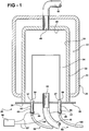
- a manufacturing apparatus 20 for deposition of a material 22 on a carrier body 24 is shown in Figures 1 and 6.
- the material 22 to be deposited is silicon; however, it is to be appreciated that the manufacturing apparatus 20 can be used to deposit other materials on the carrier body 24 without deviating from the scope of the subject invention.
- the carrier body 24 is substantially U-shaped and has a first end 54 and a second end 56 spaced and parallel to each other.
- a socket 57 is disposed at each of the first end 54 and the second end 56 of the carrier body 24.
- the manufacturing apparatus 20 includes a housing 28 that defines a chamber 30.
- the housing 28 comprises an interior cylinder 32, an outer cylinder 34, and a base plate 36.
- the interior cylinder 32 includes an open end 38 and a closed end 40 spaced from each other.
- the outer cylinder 34 is disposed about the interior cylinder 32 to define a void 42 between the interior cylinder 32 and the outer cylinder 34, typically serving as a jacket to house a circulated cooling fluid (not shown).
- the void 42 can be, but is not limited to, a conventional vessel jacket, a baffled jacket, or a half-pipe jacket.
- the base plate 36 is disposed on the open end 38 of the interior cylinder 32 to define the chamber 30.
- the base plate 36 includes a seal (not shown) disposed in alignment with the interior cylinder 32 for sealing the chamber 30 once the interior cylinder 32 is disposed on the base plate 36.
- the manufacturing apparatus 20 is a Siemens type chemical vapor deposition reactor.
- the housing 28 defines an inlet 44 for introducing a gas 45 into the chamber 30 and an outlet 46 for exhausting the gas 45 from the chamber 30.
- an inlet pipe 48 is connected to the inlet 44 for delivering the gas 45 to the housing 28 and an exhaust pipe 50 is connected to the outlet 46 for removing the gas 45 from the housing 28.
- the exhaust pipe 50 can be jacketed with a cooling fluid such as water or a commercial heat transfer fluid.
- At least one electrode 52 is disposed through the housing 28 for coupling with the socket 57.
- the at least one electrode 52 includes a first electrode 52 disposed through the housing 28 for receiving the socket 57 of the first end 54 of the carrier body 24 and a second electrode 52 disposed through the housing 28 for receiving the socket 57 of the second end 56 of the carrier body 24.
- the electrode 52 can be any type of electrode known in the art such as, for example, a flat head electrode, a two-part electrode or a cup electrode.
- the at least one electrode 52 is at least partially disposed within the chamber 30. In one embodiment, the electrode 52 is disposed through the base plate 36.
- the electrode 52 comprises an electrically conductive material having a minimum electrical conductivity at room temperature of at least 14 ⁇ 10 6 Siemens/meter or S/m.
- the electrode 52 can comprise at least one of copper, silver, nickel, Inconel and gold, each of which meets the conductivity parameters set forth above.
- the electrode 52 can comprise an alloy that meets the conductivity parameters set forth above.
- the electrode 52 comprises electrically conductive material having a minimum electrical conductivity at room temperature of about 58 ⁇ 10 6 S/m.
- the electrode 52 comprises copper and the copper is typically present in an amount of about 100% by weight based on the weight of the electrode 52.
- the copper can be oxygen-free electrolytic copper grade UNS 10100.
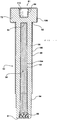
- the electrode 52 has an exterior surface 60.
- the exterior surface 60 of the electrode 52 has a contact region 80.
- the contact region 80 as defined herein is the portion of the exterior surface 60 of the electrode 52 that is adapted to be in direct contact with the socket 57 and that provides a primary current path from the electrode 52 to the socket 57 and into the carrier body 24. As such, during normal operation of the manufacturing apparatus 20, the contact region 80 is shielded from exposure to the material 22 that is deposited on the carrier body 24.
- the contact region 80 is adapted to be in direct contact with the socket 57 and is generally not exposed to the material 22 during deposition on the carrier body 24, the contact region 80 is subject to different design considerations than other portions of the electrode 52, which considerations are described in further detail below.
- the electrode 52 includes a shaft 58 having a first end 61 and a second end 62. When present, the shaft 58 further defines the exterior surface 60 of the electrode 52. Generally, the first end 61 is an open end of the electrode 52.
- the shaft 58 has a circular cross sectional shape resulting in a cylindrically-shaped shaft and defines a diameter D 1 . However, it is to be appreciated that the shaft 58 can have a rectangular, a triangular, or an elliptical cross sectional shape without deviating from the subject invention.
- the electrode 52 can also include a head 72 disposed on one of the ends 61, 62 of the shaft 58. It is to be appreciated that the head 72 can be integral to the shaft 58. Typically, when the head 72 is present, the head 72 further defines the exterior surface 60 having the contact region 80. It is to be appreciated by those skilled in the art that the method of connecting the socket 57 to the electrode 52 can vary between applications without deviating from the subject invention. For example, in one embodiment, such as for flat head electrodes (not shown), the contact region can merely be a top, flat surface on the head 72 of the electrode 52 and the socket 57 can define a socket cup (not shown) that fits over the head 72 of the electrode 52 for contacting the contact region.
- the head 72 may be absent from the ends 61, 62 of the shaft 58.
- the electrode 52 may define the contact region on the exterior surface 60 of the shaft 58, and the socket 57 may be structured as a cap that fits over the shaft 58 of the electrode 52 for contacting the contact region 80 located on the exterior surface 60 of the shaft 58.
- the electrode 52 defines a cup 81 for receiving the socket 57.
- the contact region 80 is located within a portion of the cup 81.
- the socket 57 and the cup 81 can be designed such that the socket 57 can be removed from the electrode 52 when the carrier body 24 is harvested from the manufacturing apparatus 20.
- the head 72 defines a diameter D 2 that is greater than the diameter D 1 of the shaft 58.
- the base plate 36 defines a hole (not numbered) for receiving the shaft 58 of the electrode 52 such that the head 72 of the electrode 52 remains within the chamber 30 for sealing the chamber 30. It is to be appreciated that the head 72 can be integral to the shaft 58.
- a first set of threads 84 can be disposed on the exterior surface 60 of the electrode 52.
- a dielectric sleeve 86 is typically disposed around the electrode 52 for insulating the electrode 52.
- the dielectric sleeve 86 can comprise a ceramic.
- a nut 88 is disposed on the first set of threads 84 for compressing the dielectric sleeve 86 between the base plate 36 and the nut 88 to secure the electrode 52 to the housing 28. It is to be appreciated that the electrode 52 can be secured to the housing 28 by other methods, such as by a flange, without deviating from the scope of the subject invention.
- At least one of the shaft 58 and the head 72 include an interior surface 62 defining the channel 64.
- the interior surface 62 includes a terminal end 94 spaced from the first end 61 of the shaft 58.
- the terminal end 94 is generally flat and parallel to the first end 61 of the electrode 52. It is to be appreciated that other configurations of the terminal end 94 can be utilized such as a cone-shaped configuration, an ellipse-shaped configuration, or an inverted cone-shaped configuration (none of which are shown).
- the channel 64 has a length L that extends from the first end 61 of the electrode to the terminal end 94. It is to be appreciated that the terminal end 94 can be disposed within the shaft 58 of the electrode 52 or the terminal end 94 can be disposed within the head 72 of the electrode, when present, without deviating from the subject invention.
- the manufacturing apparatus 20 further includes a power supply device 96 coupled to the electrode 52 for providing an electrical current to the electrode 52.
- a power supply device 96 coupled to the electrode 52 for providing an electrical current to the electrode 52.
- an electric wire or cable 97 couples the power supply device 96 to the electrode 52.
- the electric wire 97 is connected to the electrode 52 by disposing the electric wire 97 between the first set of threads 84 and the nut 88. It is to be appreciated that the connection of the electric wire 97 to the electrode 52 can be accomplished by different methods.
- the electrode 52 has a temperature, which is modified by passage of the electrical current there through, resulting in a heating of the electrode 52 and thereby establishing an operating temperature of the electrode.
- Such heating is known to those skilled in the art as Joule heating.
- the electrical current passes through the electrode 52, through the socket 57 and into the carrier body 24 resulting in the Joule heating of the carrier body 24.
- the Joule heating of the carrier body 24 results in a radiant/convective heating of the chamber 30.
- the passage of electrical current through the carrier body 24 establishes an operating temperature of the carrier body 24.
- the manufacturing apparatus 20 can also include a circulating system 98 disposed within the channel 64 of the electrode 52.
- the circulating system 98 is at least partially disposed within the channel 64. It is to be appreciated that a portion of the circulating system 98 can be disposed outside the channel 64.
- a second set of threads 99 can be disposed on the interior surface 62 of the electrode 52 for coupling the circulating system 98 to the electrode 52.
- fastening methods such as use of flanges or couplings, can be used to couple the circulating system 98 to the electrode.
- the circulating system 98 includes a coolant in fluid communication with the channel 64 of the electrode 52 for reducing the temperature of the electrode 52.
- the coolant is water; however, it is to be appreciated that the coolant can be any fluid designed to reduce heat through circulation without deviating from the subject invention.
- the circulating system 98 also includes a hose 100 coupled between the electrode 52 and a reservoir (not shown).
- the hose 100 includes an inner tube 101 and an outer tube 102. It is to be appreciated that the inner tube 101 and the outer tube 102 can be integral to the hose 100 or, alternatively, the inner tube 101 and the outer tube 102 can be attached to the hose 100 by utilizing couplings (not shown).
- the inner tube 101 is disposed within the channel 64 and extends a majority of the length L of the channel 64 for circulating the coolant within the electrode 52.
- the coolant within the circulating system 98 is under pressure to force the coolant through the inner tube 101 and the outer tubes 102.
- the coolant exits the inner tube 101 and is forced against the terminal end 94 of the interior surface 62 of the electrode 52 and subsequently exits the channel 64 via the outer tube 102 of the hose 100.
- reversing the flow configuration such that the coolant enters the channel 64 via the outer tube 102 and exits the channel 64 via the inner tube 101 is also possible.
- the configuration of the terminal end 94 influences the rate of heat transfer due to the surface area and proximity to the head 72 of the electrode 52. As set forth above, the different geometric contours of the terminal end 94 result in different convective heat transfer coefficients for the same circulation flow rate.
- the electrode 52 includes an exterior coating 106 disposed on the exterior surface 60 thereof outside of the contact region 80.
- the exterior coating 106 is typically disposed on at least one of the head 72, outside of the contact region 80, and the shaft 58 of the electrode 52.
- the exterior coating 106 may be disposed on the head 72 outside of the contact region 80, on the shaft 58, or on both the head 72 outside of the contact region 80 and on the shaft 58.
- the exterior coating 106 may extend from the head 72 to the first set of threads 84 on the shaft 58.
- the exterior coating 106 has an electrical conductivity of at least 9x10 6 S/m, more typically at least 20 S/m, most typically at least 40 S/m, and a corrosion resistance higher than silver in a galvanic series based upon room temperature seawater as an electrolyte. Such galvanic series tests are well known in the art. Due to a lesser importance of electrical conductivity for the exterior coating 106 than for the electrode 52 itself, and because the exterior coating 106 is not intended to be in contact with the carrier body 24 during deposition, a wider range of materials may be used for the exterior coating 106 than can be used for portions of the electrode 52 that are intended to be in contact with the carrier body 24.
- the specific type of material used for the exterior coating 106 may depend upon the specific location of the exterior coating 106.
- the source of corrosion and, thus, fouling may be different depending upon the specific location of the exterior coating 106.
- the exterior coating 106 is disposed on the exterior surface 60 of the head 72 outside of the contact region 80, the exterior coating 106 is disposed within the chamber 30 and, thus, is exposed to the material 22 that is used to deposit on the carrier body 24.
- Suitable metals that may be used for the exterior coating 106 on the head 72 of the electrode 52 outside of the contact region 80 include gold, platinum, and palladium.
- the exterior coating 106 comprises gold due to an excellent combination of electrical conductivity and resistance to corrosion from various sources.
- the exterior coating 106 may include other metals so long as at least one of gold, platinum, and palladium are included in the exterior coating 106.
- the exterior coating 106 may further include at least one of silver, nickel, and chromium, such as a nickel/silver alloy.
- the exterior coating 106 includes substantially only gold, platinum, and/or palladium.
- the total amount of gold, platinum, and palladium is typically at least 50 % by weight based on the total weight of the exterior coating 106.
- the exterior coating 106 may include the same or different metals from those included in the exterior coating 106 on the head 72 outside of the contact region 80.
- the exterior coating 106 on the shaft 58 includes different materials from the exterior surface 60 of the head 72, thereby allowing the exterior coating 106 on the shaft 58 to be tailored to resist corrosion from different sources than the cause of corrosion on the exterior surface 60 of the head 72.
- the shaft 72 may be free from a coating disposed on the exterior surface 60 thereof.
- the exterior surface 60 of the head may be free from a coating, with the exterior coating 106 only disposed on the exterior surface 60 of the shaft 58.
- the exterior coating 106 typically has a thickness of from 0.0254 mm to 0.254 mm, more typically from 0.0508 mm to 0.254 mm and most typically from 0.127 mm to 0.254 mm.
- the electrode 52 can be coated in other locations other than the exterior surface 60 for extending the life of the electrode 52.
- a channel coating 104 may be disposed on the interior surface 62 of the electrode 52 for maintaining the thermal conductivity between the electrode 52 and the coolant.
- the channel coating 104 has a higher resistance to corrosion that is caused by the interaction of the coolant with the interior surface 62 as compared to the resistance to corrosion of the electrode 52.
- the channel coating 104 typically includes a metal that resists corrosion and that inhibits buildup of deposits.
- the channel coating 104 can comprise at least one of silver, gold, nickel, and chromium.
- the channel coating 104 is nickel.
- the channel coating 104 has a thermal conductivity of from 70.3 to 427 W/m K, more typically from 70.3 to 405 W/m K and most typically from 70.3 to 90.5 W/m K.
- the channel coating 104 also has a thickness of from 0.0025 mm to 0.026 mm, more typically from 0.0025 mm to 0.0127 mm and most typically from 0.0051 mm to 0.0127 mm.
- the electrode 52 may further include an anti-tarnishing layer disposed on the channel coating 104.
- the anti-tarnishing layer is a protective thin film organic layer that is applied on top of the channel coating 104.
- Protective systems such as Technic Inc.'s TarnibanTM can be used following the formation of the channel coating 104 of the electrode 52 to reduce oxidation of the metal in the electrode 52 and in the channel coating 104 without inducing excessive thermal resistance.
- the electrode 52 can comprise silver and the channel coating 104 can comprise silver with the anti-tarnishing layer present for providing enhanced resistance to the formation of deposits compared to pure silver.
- the electrode 52 comprises copper and the channel coating 104 comprises nickel for maximizing thermal conductivity and resistance to the formation of deposits, with the anti-tarnishing layer disposed on the channel coating 104.
- the delay of fouling attributed to the presence of the channel coating 104 extends the life of the electrode 52.
- Increasing the life of the electrode 52 decreases production cost as the electrode 52 needs to be replaced less often as compared to electrodes 52 without the channel coating 104.
- the production time to deposit the material 22 on the carrier body 24 is also decreased because replacement of electrodes 52 is less frequent compared to when electrodes 52 are used without the channel coating 104.
- the channel coating 104 results in less down time for the manufacturing apparatus 20.
- the electrode 52 includes a contact region coating 110 disposed on the contact region 80 of the electrode 52.
- the contact region coating 110 generally comprises a metal.
- the contact region coating 110 can comprise at least one of silver, gold, nickel, and chromium.
- the contact region coating 110 comprises nickel or silver.
- the contact region coating 110 has a thickness of from 0.00254 to 0.254 mm, more typically from 0.00508 mm to 0.127 mm and most typically from 0.00508 mm to 0.0254 mm.
- the exterior coating 106 when the exterior coating 106 is disposed on the head 72 outside of the contact region 80, the exterior coating 106 can comprise nickel or chromium due to chlorination resistance while the use of silver for the contact region coating 110 may be chosen for silicidation resistance over natural resistance to chloride attack. Further, because silver is more electrically conductive than nickel or chromium, the silver may be more appropriate for the contact region coating 110 than nickel or chromium whereas electrical conductivity is of lesser importance outside of the contact region 80.
- the contact region coating 110 also provides improved electrical conduction and minimizes a copper silicide buildup within the contact region 80.
- the copper silicide buildup prevents a proper fit between the socket 57 and the contact region 80 which can lead to a pitting of the socket 57. The pitting causes small electric arcs between the contact region 80 and socket 57 that results to metal contamination of the polycrystalline silicon product.
- the electrode 52 can have at least one of the channel coating 104 and the contact region coating 110 in any combination in addition to the exterior coating 106.
- the channel coating 104, the exterior coating 106, and the contact region coating 110 can be formed by electroplating.
- the each of the coatings can be formed by different methods without deviating from the subject invention.
- some plating processes utilize materials that are dopants, e.g. Group III and Group V elements (excluding nitrogen for the case of manufacturing polycrystalline silicon), and choice of the appropriate coating method can minimize the potential contamination of the carrier body 24.
- a typical method of deposition of the material 22 on the carrier body 24 is discussed below and refers to Figure 6.
- the carrier body 24 is placed within the chamber 30 such that the sockets 57 disposed at the first end 54 and the second end 56 of the carrier body 24 are disposed within the cup 81 of the electrode 52 and the chamber 30 is sealed.
- the electrical current is transferred from the power supply device 96 to the electrode 52.
- a deposition temperature is calculated based on the material 22 to be deposited.
- the operating temperature of the carrier body 24 is increased by direct passage of the electrical current to the carrier body 24 so that the operating temperature of the carrier body 24 exceeds the deposition temperature.
- the gas 45 is introduced into the chamber 30 once the carrier body 24 reaches the deposition temperature.
- the gas 45 introduced into the chamber 30 comprises a halosilane, such as a chlorosilane or a bromosilane.
- the gas can further comprise hydrogen.
- the instant invention is not limited to the components present in the gas and that the gas can comprise other deposition precursors, especially silicon containing molecular such as silane, silicon tetrachloride, and tribromosilane.
- the carrier body 24 is a silicon slim rod and the manufacturing apparatus 20 can be used to deposit silicon thereon.
- the gas typically contains trichlorosilane and silicon is deposited onto the carrier body 24 as a result of the thermal decomposition of trichlorosilane.
- the coolant is utilized for preventing the operating temperature of the electrode 52 from reaching the deposition temperature to ensure that silicon is not deposited on the electrode 52.
- the material 22 is deposited evenly onto the carrier body 24 until a desired diameter of material 22 on the carrier body 24 is reached.
- the electrical current is interrupted so that the electrode 52 and the carrier body 24 stop receiving the electrical current.
- the gas 45 is exhausted through the outlet 46 of the housing 28 and the carrier body 24 is allowed to cool. Once the operating temperature of the processed carrier body 24 has cooled the processed carrier body 24 can be removed from the chamber 30. The processed carrier body 24 is then removed and a new carrier body 24 is placed in the manufacturing apparatus 20.
Claims (15)
- Appareil de fabrication pour le dépôt d'un matériau (22) sur un corps de support (24) ayant une première extrémité (54) et une seconde extrémité (56) espacées l'une de l'autre avec une douille (57) disposée à chaque extrémité du corps de support (24), ledit appareil (20) comprenant :un logement (28) définissant une chambre (30) ;un orifice d'admission (44) défini à travers ledit logement (28) pour l'introduction d'un gaz (45) dans la chambre (30) ;un orifice de refoulement (46) défini à travers ledit logement (28) pour l'échappement du gaz (45) depuis la chambre (30) ;au moins une électrode (52) ayant une surface extérieure (60) ayant une région de contact (80) adaptée pour venir en contact avec la douille (57), ladite électrode (52) étant disposée à travers ledit logement (28) avec ladite électrode (52) disposée au moins partiellement au sein de la chambre (30) pour se coupler à la douille (57) ; etun dispositif d'alimentation électrique (96) couplé à ladite électrode (52) pour fournir un courant électrique à ladite électrode (52) ;caractérisé par :un revêtement extérieur (106) disposé sur ladite surface extérieure (60) de ladite électrode (52) à l'extérieur de ladite région de contact (80), ledit revêtement extérieur (106) ayant une conductivité électrique d'au moins 9 x 10⁶ Siemens/mètre et une résistance à la corrosion supérieure à l'argent dans une série galvanique sur la base de l'eau de mer à température ambiante en tant qu'électrolyte.
- Appareil de fabrication selon la revendication 1, dans lequel ladite électrode (52) comporte en outre :une tige (58) ayant une première extrémité (61) et une seconde extrémité (62) ; etune tête (72) disposée sur l'une desdites extrémités (61, 62) de ladite tige (58).
- Appareil de fabrication selon la revendication 2, dans lequel ladite tête (72) de ladite électrode (52) définit ladite surface extérieure (60) ayant ladite région de contact (80).
- Appareil de fabrication selon la revendication 3, dans lequel ledit revêtement extérieur (106) est disposé sur ladite tête (72) à l'extérieur de ladite région de contact (80).
- Appareil de fabrication selon la revendication 4, dans lequel ledit revêtement extérieur (106) est en outre disposé sur ladite tige (58) de ladite électrode (52) et dans lequel ledit revêtement extérieur (106) sur ladite tige (58) comporte des métaux différents dudit revêtement extérieur (106) sur ladite tête (72).
- Appareil de fabrication selon l'une quelconque des revendications 2 à 5, dans lequel ladite tête (72) comprend du cuivre et ladite tête (72) de ladite électrode (52) est disposée au moins partiellement au sein de la chambre (30).
- Appareil de fabrication selon une quelconque revendication précédente, dans lequel ledit revêtement extérieur (106) comprend au moins un élément parmi l'or, le platine, et le palladium.
- Appareil de fabrication selon la revendication 7, dans lequel ledit revêtement extérieur (106) comprend en outre au moins un élément parmi l'argent, le nickel, et le chrome.
- Appareil de fabrication selon une quelconque revendication précédente, dans lequel ledit revêtement extérieur (106) a une épaisseur de 0,0254 à 0,254 mm.
- Électrode à utiliser avec un appareil de fabrication (20) pour déposer un matériau (22) sur un corps de support (24) ayant une première extrémité (54) et une seconde extrémité (56) espacées l'une de l'autre avec une douille (57) disposée à chaque extrémité du corps de support (24), ladite électrode (52) comprenant :une tige (58) ayant une première extrémité (61) et une seconde extrémité (62) ;une tête (72) disposée sur l'une desdites extrémités (61, 62) de ladite tige (58) pour se coupler à la douille (57) ;dans laquelle ladite tige (58) et ladite tête (72) ont une surface extérieure (60) ayant une région de contact (80) adaptée pour venir en contact avec la douille (57) ; etladite électrode (52) ayant une surface extérieure (60) ;caractérisée par :un revêtement extérieur (106) disposé sur ladite surface extérieure (60) à l'extérieur de ladite région de contact (80), ledit revêtement extérieur (106) ayant une conductivité électrique d'au moins 9 x 10⁶ Siemens/mètre et une résistance à la corrosion supérieure à l'argent dans une série galvanique sur la base de l'eau de mer à température ambiante en tant qu'électrolyte.
- Électrode selon la revendication 10, dans laquelle ladite électrode (52) définit une cuvette (81) avec ladite région de contact (80) située au sein d'une portion de ladite cuvette (81).
- Électrode selon la revendication 11, dans laquelle ledit revêtement extérieur (106) est disposé sur ladite tête (72) à l'extérieur de ladite région de contact (80).
- Électrode selon l'une quelconque des revendications 10 à 12, dans laquelle ledit revêtement extérieur (106) comprend au moins un élément parmi l'or, le platine, et le palladium.
- Électrode selon la revendication 13, dans laquelle ledit revêtement extérieur (106) comprend en outre au moins un élément parmi l'argent, le nickel, et le chrome.
- Électrode selon l'une quelconque des revendications 10 à 14, dans laquelle ledit revêtement extérieur (106) a une épaisseur de 0,0254 à 0,254 mm.
Applications Claiming Priority (2)
| Application Number | Priority Date | Filing Date | Title |
|---|---|---|---|
| US4468708P | 2008-04-14 | 2008-04-14 | |
| PCT/US2009/002294 WO2009128888A1 (fr) | 2008-04-14 | 2009-04-13 | Appareil de fabrication destiné à déposer un matériau et électrode utilisée dans un tel appareil |
Publications (2)
| Publication Number | Publication Date |
|---|---|
| EP2266369A1 EP2266369A1 (fr) | 2010-12-29 |
| EP2266369B1 true EP2266369B1 (fr) | 2017-11-22 |
Family
ID=40791646
Family Applications (1)
| Application Number | Title | Priority Date | Filing Date |
|---|---|---|---|
| EP09732543.5A Not-in-force EP2266369B1 (fr) | 2008-04-14 | 2009-04-13 | Appareil de fabrication destiné à déposer un matériau et électrode utilisée dans un tel appareil |
Country Status (10)
| Country | Link |
|---|---|
| US (2) | US8951352B2 (fr) |
| EP (1) | EP2266369B1 (fr) |
| JP (2) | JP5959198B2 (fr) |
| KR (1) | KR101552501B1 (fr) |
| CN (1) | CN102047751B (fr) |
| AU (1) | AU2009236679B2 (fr) |
| CA (1) | CA2721095A1 (fr) |
| RU (1) | RU2494579C2 (fr) |
| TW (1) | TWI505743B (fr) |
| WO (1) | WO2009128888A1 (fr) |
Families Citing this family (4)
| Publication number | Priority date | Publication date | Assignee | Title |
|---|---|---|---|---|
| JP5762949B2 (ja) | 2008-04-14 | 2015-08-12 | ヘムロック・セミコンダクター・コーポレーション | 材料を蒸着するための製造装置及び当該装置において使用される電極 |
| JP5477145B2 (ja) * | 2009-04-28 | 2014-04-23 | 三菱マテリアル株式会社 | 多結晶シリコン反応炉 |
| JP5699060B2 (ja) * | 2011-09-20 | 2015-04-08 | 信越化学工業株式会社 | 多結晶シリコンの製造方法 |
| TWI735439B (zh) * | 2015-04-14 | 2021-08-11 | 美商安芬諾股份有限公司 | 電連接器 |
Family Cites Families (67)
| Publication number | Priority date | Publication date | Assignee | Title |
|---|---|---|---|---|
| GB1054141A (fr) | 1900-01-01 | |||
| US1738828A (en) * | 1925-03-02 | 1929-12-10 | Jackson Arthur Hews | Low-resistance permanent wire |
| US3330251A (en) | 1955-11-02 | 1967-07-11 | Siemens Ag | Apparatus for producing highest-purity silicon for electric semiconductor devices |
| US3011877A (en) | 1956-06-25 | 1961-12-05 | Siemens Ag | Production of high-purity semiconductor materials for electrical purposes |
| NL238464A (fr) | 1958-05-29 | |||
| DE1150366B (de) | 1958-12-09 | 1963-06-20 | Siemens Ag | Verfahren zur Herstellung von Reinstsilicium |
| NL251143A (fr) | 1959-05-04 | |||
| DE1155759B (de) | 1959-06-11 | 1963-10-17 | Siemens Ag | Vorrichtung zur Gewinnung reinsten kristallinen Halbleitermaterials fuer elektrotechnische Zwecke |
| DE1223804B (de) * | 1961-01-26 | 1966-09-01 | Siemens Ag | Vorrichtung zur Gewinnung reinen Halbleitermaterials, wie Silicium |
| DE1264400B (de) | 1961-01-26 | 1968-03-28 | Siemens Ag | Vorrichtung zur Gewinnung reinen Halbleitermaterials aus der Gasphase |
| DE1138481C2 (de) | 1961-06-09 | 1963-05-22 | Siemens Ag | Verfahren zur Herstellung von Halbleiteranordnungen durch einkristalline Abscheidung von Halbleitermaterial aus der Gasphase |
| DE2324365C3 (de) | 1973-05-14 | 1978-05-11 | Siemens Ag, 1000 Berlin Und 8000 Muenchen | Reaktionsgefäß zum Abscheiden von Halbleitermaterial auf erhitzte Trägerkörper |
| DE2541215C3 (de) | 1975-09-16 | 1978-08-03 | Wacker-Chemitronic Gesellschaft Fuer Elektronik-Grundstoffe Mbh, 8263 Burghausen | Verfahren zur Herstellung von Siliciumhohlkörpern |
| DE2652218A1 (de) | 1976-11-16 | 1978-05-24 | Wacker Chemitronic | Verfahren zur herstellung von substratgebundenem, grossflaechigem silicium |
| JPS53106626A (en) * | 1977-03-02 | 1978-09-16 | Komatsu Mfg Co Ltd | Method of making high purity rod silicon and appratus therefor |
| JPS53108029A (en) | 1977-03-03 | 1978-09-20 | Komatsu Mfg Co Ltd | Method of making high purity silicon having uniform shape |
| US4173944A (en) | 1977-05-20 | 1979-11-13 | Wacker-Chemitronic Gesellschaft Fur Elektronik-Grundstoffe Mbh | Silverplated vapor deposition chamber |
| US4179530A (en) * | 1977-05-20 | 1979-12-18 | Wacker-Chemitronic Gesellschaft Fur Elektronik-Grundstoffe Mbh | Process for the deposition of pure semiconductor material |
| DE2912661C2 (de) | 1979-03-30 | 1982-06-24 | Wacker-Chemitronic Gesellschaft Fuer Elektronik-Grundstoffe Mbh, 8263 Burghausen | Verfahren zur Abscheidung von reinem Halbleitermaterial und Düse zur Durchführung des Verfahrens |
| US4304641A (en) | 1980-11-24 | 1981-12-08 | International Business Machines Corporation | Rotary electroplating cell with controlled current distribution |
| US4477911A (en) | 1982-12-02 | 1984-10-16 | Westinghouse Electric Corp. | Integral heat pipe-electrode |
| US4481232A (en) | 1983-05-27 | 1984-11-06 | The United States Of America As Represented By The Department Of Energy | Method and apparatus for producing high purity silicon |
| US4466864A (en) * | 1983-12-16 | 1984-08-21 | At&T Technologies, Inc. | Methods of and apparatus for electroplating preselected surface regions of electrical articles |
| US4822641A (en) | 1985-04-30 | 1989-04-18 | Inovan Gmbh & Co. Kg | Method of manufacturing a contact construction material structure |
| SE452862B (sv) | 1985-06-05 | 1987-12-21 | Aga Ab | Ljusbagselektrod |
| US4707225A (en) | 1986-01-06 | 1987-11-17 | Rockwell International Corporation | Fluid-cooled channel construction |
| US4805556A (en) | 1988-01-15 | 1989-02-21 | Union Carbide Corporation | Reactor system and method for forming uniformly large-diameter polycrystalline rods by the pyrolysis of silane |
| US5096550A (en) | 1990-10-15 | 1992-03-17 | The United States Of America As Represented By The United States Department Of Energy | Method and apparatus for spatially uniform electropolishing and electrolytic etching |
| RU2020777C1 (ru) * | 1991-07-03 | 1994-09-30 | Нижегородский научно-исследовательский приборостроительный институт "Кварц" | Способ металлизации подложки из фторопласта |
| US5139890A (en) * | 1991-09-30 | 1992-08-18 | Olin Corporation | Silver-coated electrical components |
| US5906799A (en) | 1992-06-01 | 1999-05-25 | Hemlock Semiconductor Corporation | Chlorosilane and hydrogen reactor |
| US5227041A (en) | 1992-06-12 | 1993-07-13 | Digital Equipment Corporation | Dry contact electroplating apparatus |
| DE4243570C1 (de) | 1992-12-22 | 1994-01-27 | Heraeus Gmbh W C | Elektrischer Kontaktkörper |
| RU2052538C1 (ru) * | 1993-04-08 | 1996-01-20 | Сергей Николаевич Кучанов | Способ нанесения вакуумного металлизированного покрытия на диэлектрические подложки |
| US5422088A (en) | 1994-01-28 | 1995-06-06 | Hemlock Semiconductor Corporation | Process for hydrogenation of tetrachlorosilane |
| JP3377849B2 (ja) | 1994-02-02 | 2003-02-17 | 日本エレクトロプレイテイング・エンジニヤース株式会社 | ウエーハ用メッキ装置 |
| DE4424929C2 (de) | 1994-07-14 | 1997-02-13 | Wacker Chemie Gmbh | Halterung für Trägerkörper in einer Vorrichtung zur Abscheidung von Halbleitermaterial |
| US5567300A (en) | 1994-09-02 | 1996-10-22 | Ibm Corporation | Electrochemical metal removal technique for planarization of surfaces |
| FR2741227A1 (fr) | 1995-11-14 | 1997-05-16 | Verrerie & Cristallerie | Electrode, notamment destinee a etre utilisee dans des fours de fusion du verre |
| US5911619A (en) | 1997-03-26 | 1999-06-15 | International Business Machines Corporation | Apparatus for electrochemical mechanical planarization |
| US5807165A (en) | 1997-03-26 | 1998-09-15 | International Business Machines Corporation | Method of electrochemical mechanical planarization |
| NL1005963C2 (nl) | 1997-05-02 | 1998-11-09 | Asm Int | Verticale oven voor het behandelen van halfgeleidersubstraten. |
| RU2135629C1 (ru) | 1997-11-12 | 1999-08-27 | Государственное предприятие ВНИИавтогенмаш | Способ повышения долговечности электродных и сопловых устройств и технологический плазматрон для его осуществления |
| US6544333B2 (en) * | 1997-12-15 | 2003-04-08 | Advanced Silicon Materials Llc | Chemical vapor deposition system for polycrystalline silicon rod production |
| DE19882883B4 (de) * | 1997-12-15 | 2009-02-26 | Advanced Silicon Materials LLC, (n.d.Ges.d.Staates Delaware), Moses Lake | System für die chemische Abscheidung aus der Gasphase zum Herstellen polykristalliner Siliziumstangen |
| US6004880A (en) | 1998-02-20 | 1999-12-21 | Lsi Logic Corporation | Method of single step damascene process for deposition and global planarization |
| US6176992B1 (en) | 1998-11-03 | 2001-01-23 | Nutool, Inc. | Method and apparatus for electro-chemical mechanical deposition |
| AU3375000A (en) | 1999-02-19 | 2000-09-04 | Gt Equipment Technologies Inc. | Method and apparatus for chemical vapor deposition of polysilicon |
| JP4372918B2 (ja) | 1999-06-30 | 2009-11-25 | パナソニック電工株式会社 | プラズマ処理装置及びプラズマ処理方法 |
| JP2001156042A (ja) | 1999-11-29 | 2001-06-08 | Hitachi Ltd | プラズマ処理装置 |
| DE10005821A1 (de) * | 2000-02-10 | 2001-08-23 | Schott Glas | Gekühlte Edelmetallelektrode zum Einstellen einer bestimmten Elektrodenoberfläche |
| DE10041564C2 (de) | 2000-08-24 | 2002-06-27 | Heraeus Noblelight Gmbh | Kühlbares Infrarotstrahlerelement |
| DE10101040A1 (de) | 2001-01-11 | 2002-07-25 | Wacker Chemie Gmbh | Vorrichtung und Verfahren zur Herstellung eines polykristallinen Siliciumstabes |
| JP2002231357A (ja) * | 2001-02-06 | 2002-08-16 | Nagano Fujitsu Component Kk | 電気接点およびコネクタ |
| JP4402860B2 (ja) | 2001-03-28 | 2010-01-20 | 忠弘 大見 | プラズマ処理装置 |
| JP2002313533A (ja) * | 2001-04-17 | 2002-10-25 | Toshiba Ceramics Co Ltd | 面状セラミックスヒーター |
| US6623801B2 (en) * | 2001-07-30 | 2003-09-23 | Komatsu Ltd. | Method of producing high-purity polycrystalline silicon |
| JP3870824B2 (ja) * | 2001-09-11 | 2007-01-24 | 住友電気工業株式会社 | 被処理物保持体、半導体製造装置用サセプタおよび処理装置 |
| GB0213402D0 (en) * | 2002-06-12 | 2002-07-24 | Johnson Matthey Plc | Improvements in coated equipment |
| JP2004205059A (ja) | 2002-12-20 | 2004-07-22 | Toyo Radiator Co Ltd | 高耐蝕性熱交換器の製造方法 |
| JP2005272965A (ja) * | 2004-03-25 | 2005-10-06 | Sumitomo Heavy Ind Ltd | 電極部材、及びこれを備えた成膜装置 |
| JP4031782B2 (ja) | 2004-07-01 | 2008-01-09 | 株式会社大阪チタニウムテクノロジーズ | 多結晶シリコン製造方法およびシード保持電極 |
| JP2007281161A (ja) | 2006-04-06 | 2007-10-25 | Sumitomo Electric Ind Ltd | 半導体製造装置用ウエハ保持体及び半導体製造装置 |
| US9683286B2 (en) | 2006-04-28 | 2017-06-20 | Gtat Corporation | Increased polysilicon deposition in a CVD reactor |
| KR100768148B1 (ko) | 2006-05-22 | 2007-10-17 | 한국화학연구원 | 금속 코어수단을 이용한 다결정 실리콘 봉의 제조방법 |
| WO2009128886A1 (fr) | 2008-04-14 | 2009-10-22 | Hemlock Semiconductor Corporation | Appareil de fabrication pour déposer un matériau et électrode destinée à être utilisée dans celui-ci |
| JP5762949B2 (ja) | 2008-04-14 | 2015-08-12 | ヘムロック・セミコンダクター・コーポレーション | 材料を蒸着するための製造装置及び当該装置において使用される電極 |
-
2009
- 2009-04-13 KR KR1020107025442A patent/KR101552501B1/ko active IP Right Grant
- 2009-04-13 EP EP09732543.5A patent/EP2266369B1/fr not_active Not-in-force
- 2009-04-13 US US12/937,802 patent/US8951352B2/en not_active Expired - Fee Related
- 2009-04-13 AU AU2009236679A patent/AU2009236679B2/en not_active Ceased
- 2009-04-13 RU RU2010146253/07A patent/RU2494579C2/ru not_active IP Right Cessation
- 2009-04-13 CN CN200980120357.0A patent/CN102047751B/zh not_active Expired - Fee Related
- 2009-04-13 WO PCT/US2009/002294 patent/WO2009128888A1/fr active Application Filing
- 2009-04-13 CA CA2721095A patent/CA2721095A1/fr not_active Abandoned
- 2009-04-13 JP JP2011505007A patent/JP5959198B2/ja not_active Expired - Fee Related
- 2009-04-14 TW TW098112368A patent/TWI505743B/zh not_active IP Right Cessation
-
2014
- 2014-08-15 US US14/460,843 patent/US20140353147A1/en not_active Abandoned
- 2014-09-19 JP JP2014191023A patent/JP5909533B2/ja active Active
Also Published As
| Publication number | Publication date |
|---|---|
| US20140353147A1 (en) | 2014-12-04 |
| JP2011523758A (ja) | 2011-08-18 |
| WO2009128888A1 (fr) | 2009-10-22 |
| EP2266369A1 (fr) | 2010-12-29 |
| KR20110009146A (ko) | 2011-01-27 |
| US8951352B2 (en) | 2015-02-10 |
| JP5909533B2 (ja) | 2016-04-26 |
| CN102047751B (zh) | 2014-01-29 |
| US20110036294A1 (en) | 2011-02-17 |
| RU2010146253A (ru) | 2012-05-20 |
| TW201004460A (en) | 2010-01-16 |
| AU2009236679A1 (en) | 2009-10-22 |
| KR101552501B1 (ko) | 2015-09-14 |
| RU2494579C2 (ru) | 2013-09-27 |
| AU2009236679B2 (en) | 2014-02-27 |
| JP5959198B2 (ja) | 2016-08-02 |
| CA2721095A1 (fr) | 2009-10-22 |
| TWI505743B (zh) | 2015-10-21 |
| JP2015028217A (ja) | 2015-02-12 |
| CN102047751A (zh) | 2011-05-04 |
Similar Documents
| Publication | Publication Date | Title |
|---|---|---|
| EP2266368B1 (fr) | Appareil de fabrication destiné à déposer un matériau sur une électrode destinée à être utilisée dans ledit appareil | |
| AU2009236677B2 (en) | Manufacturing apparatus for depositing a material and an electrode for use therein | |
| US20140353147A1 (en) | Electrode for use with manufacturing apparatus |
Legal Events
| Date | Code | Title | Description |
|---|---|---|---|
| PUAI | Public reference made under article 153(3) epc to a published international application that has entered the european phase |
Free format text: ORIGINAL CODE: 0009012 |
|
| 17P | Request for examination filed |
Effective date: 20101014 |
|
| AK | Designated contracting states |
Kind code of ref document: A1 Designated state(s): AT BE BG CH CY CZ DE DK EE ES FI FR GB GR HR HU IE IS IT LI LT LU LV MC MK MT NL NO PL PT RO SE SI SK TR |
|
| AX | Request for extension of the european patent |
Extension state: AL BA RS |
|
| DAX | Request for extension of the european patent (deleted) | ||
| 17Q | First examination report despatched |
Effective date: 20130618 |
|
| RAP1 | Party data changed (applicant data changed or rights of an application transferred) |
Owner name: HEMLOCK SEMICONDUCTOR OPERATIONS LLC |
|
| GRAP | Despatch of communication of intention to grant a patent |
Free format text: ORIGINAL CODE: EPIDOSNIGR1 |
|
| STAA | Information on the status of an ep patent application or granted ep patent |
Free format text: STATUS: GRANT OF PATENT IS INTENDED |
|
| INTG | Intention to grant announced |
Effective date: 20170612 |
|
| GRAS | Grant fee paid |
Free format text: ORIGINAL CODE: EPIDOSNIGR3 |
|
| GRAA | (expected) grant |
Free format text: ORIGINAL CODE: 0009210 |
|
| STAA | Information on the status of an ep patent application or granted ep patent |
Free format text: STATUS: THE PATENT HAS BEEN GRANTED |
|
| AK | Designated contracting states |
Kind code of ref document: B1 Designated state(s): AT BE BG CH CY CZ DE DK EE ES FI FR GB GR HR HU IE IS IT LI LT LU LV MC MK MT NL NO PL PT RO SE SI SK TR |
|
| REG | Reference to a national code |
Ref country code: GB Ref legal event code: FG4D |
|
| REG | Reference to a national code |
Ref country code: CH Ref legal event code: EP |
|
| REG | Reference to a national code |
Ref country code: IE Ref legal event code: FG4D |
|
| REG | Reference to a national code |
Ref country code: AT Ref legal event code: REF Ref document number: 949512 Country of ref document: AT Kind code of ref document: T Effective date: 20171215 |
|
| REG | Reference to a national code |
Ref country code: DE Ref legal event code: R096 Ref document number: 602009049490 Country of ref document: DE |
|
| REG | Reference to a national code |
Ref country code: NL Ref legal event code: MP Effective date: 20171122 |
|
| REG | Reference to a national code |
Ref country code: LT Ref legal event code: MG4D |
|
| REG | Reference to a national code |
Ref country code: AT Ref legal event code: MK05 Ref document number: 949512 Country of ref document: AT Kind code of ref document: T Effective date: 20171122 |
|
| PG25 | Lapsed in a contracting state [announced via postgrant information from national office to epo] |
Ref country code: SE Free format text: LAPSE BECAUSE OF FAILURE TO SUBMIT A TRANSLATION OF THE DESCRIPTION OR TO PAY THE FEE WITHIN THE PRESCRIBED TIME-LIMIT Effective date: 20171122 Ref country code: FI Free format text: LAPSE BECAUSE OF FAILURE TO SUBMIT A TRANSLATION OF THE DESCRIPTION OR TO PAY THE FEE WITHIN THE PRESCRIBED TIME-LIMIT Effective date: 20171122 Ref country code: NO Free format text: LAPSE BECAUSE OF FAILURE TO SUBMIT A TRANSLATION OF THE DESCRIPTION OR TO PAY THE FEE WITHIN THE PRESCRIBED TIME-LIMIT Effective date: 20180222 Ref country code: NL Free format text: LAPSE BECAUSE OF FAILURE TO SUBMIT A TRANSLATION OF THE DESCRIPTION OR TO PAY THE FEE WITHIN THE PRESCRIBED TIME-LIMIT Effective date: 20171122 Ref country code: LT Free format text: LAPSE BECAUSE OF FAILURE TO SUBMIT A TRANSLATION OF THE DESCRIPTION OR TO PAY THE FEE WITHIN THE PRESCRIBED TIME-LIMIT Effective date: 20171122 Ref country code: ES Free format text: LAPSE BECAUSE OF FAILURE TO SUBMIT A TRANSLATION OF THE DESCRIPTION OR TO PAY THE FEE WITHIN THE PRESCRIBED TIME-LIMIT Effective date: 20171122 |
|
| PG25 | Lapsed in a contracting state [announced via postgrant information from national office to epo] |
Ref country code: LV Free format text: LAPSE BECAUSE OF FAILURE TO SUBMIT A TRANSLATION OF THE DESCRIPTION OR TO PAY THE FEE WITHIN THE PRESCRIBED TIME-LIMIT Effective date: 20171122 Ref country code: GR Free format text: LAPSE BECAUSE OF FAILURE TO SUBMIT A TRANSLATION OF THE DESCRIPTION OR TO PAY THE FEE WITHIN THE PRESCRIBED TIME-LIMIT Effective date: 20180223 Ref country code: AT Free format text: LAPSE BECAUSE OF FAILURE TO SUBMIT A TRANSLATION OF THE DESCRIPTION OR TO PAY THE FEE WITHIN THE PRESCRIBED TIME-LIMIT Effective date: 20171122 Ref country code: HR Free format text: LAPSE BECAUSE OF FAILURE TO SUBMIT A TRANSLATION OF THE DESCRIPTION OR TO PAY THE FEE WITHIN THE PRESCRIBED TIME-LIMIT Effective date: 20171122 Ref country code: BG Free format text: LAPSE BECAUSE OF FAILURE TO SUBMIT A TRANSLATION OF THE DESCRIPTION OR TO PAY THE FEE WITHIN THE PRESCRIBED TIME-LIMIT Effective date: 20180222 |
|
| PG25 | Lapsed in a contracting state [announced via postgrant information from national office to epo] |
Ref country code: EE Free format text: LAPSE BECAUSE OF FAILURE TO SUBMIT A TRANSLATION OF THE DESCRIPTION OR TO PAY THE FEE WITHIN THE PRESCRIBED TIME-LIMIT Effective date: 20171122 Ref country code: CY Free format text: LAPSE BECAUSE OF FAILURE TO SUBMIT A TRANSLATION OF THE DESCRIPTION OR TO PAY THE FEE WITHIN THE PRESCRIBED TIME-LIMIT Effective date: 20171122 Ref country code: DK Free format text: LAPSE BECAUSE OF FAILURE TO SUBMIT A TRANSLATION OF THE DESCRIPTION OR TO PAY THE FEE WITHIN THE PRESCRIBED TIME-LIMIT Effective date: 20171122 Ref country code: CZ Free format text: LAPSE BECAUSE OF FAILURE TO SUBMIT A TRANSLATION OF THE DESCRIPTION OR TO PAY THE FEE WITHIN THE PRESCRIBED TIME-LIMIT Effective date: 20171122 Ref country code: SK Free format text: LAPSE BECAUSE OF FAILURE TO SUBMIT A TRANSLATION OF THE DESCRIPTION OR TO PAY THE FEE WITHIN THE PRESCRIBED TIME-LIMIT Effective date: 20171122 |
|
| REG | Reference to a national code |
Ref country code: DE Ref legal event code: R097 Ref document number: 602009049490 Country of ref document: DE |
|
| PG25 | Lapsed in a contracting state [announced via postgrant information from national office to epo] |
Ref country code: PL Free format text: LAPSE BECAUSE OF FAILURE TO SUBMIT A TRANSLATION OF THE DESCRIPTION OR TO PAY THE FEE WITHIN THE PRESCRIBED TIME-LIMIT Effective date: 20171122 Ref country code: RO Free format text: LAPSE BECAUSE OF FAILURE TO SUBMIT A TRANSLATION OF THE DESCRIPTION OR TO PAY THE FEE WITHIN THE PRESCRIBED TIME-LIMIT Effective date: 20171122 Ref country code: IT Free format text: LAPSE BECAUSE OF FAILURE TO SUBMIT A TRANSLATION OF THE DESCRIPTION OR TO PAY THE FEE WITHIN THE PRESCRIBED TIME-LIMIT Effective date: 20171122 |
|
| PLBE | No opposition filed within time limit |
Free format text: ORIGINAL CODE: 0009261 |
|
| STAA | Information on the status of an ep patent application or granted ep patent |
Free format text: STATUS: NO OPPOSITION FILED WITHIN TIME LIMIT |
|
| 26N | No opposition filed |
Effective date: 20180823 |
|
| PG25 | Lapsed in a contracting state [announced via postgrant information from national office to epo] |
Ref country code: SI Free format text: LAPSE BECAUSE OF FAILURE TO SUBMIT A TRANSLATION OF THE DESCRIPTION OR TO PAY THE FEE WITHIN THE PRESCRIBED TIME-LIMIT Effective date: 20171122 Ref country code: MC Free format text: LAPSE BECAUSE OF FAILURE TO SUBMIT A TRANSLATION OF THE DESCRIPTION OR TO PAY THE FEE WITHIN THE PRESCRIBED TIME-LIMIT Effective date: 20171122 |
|
| REG | Reference to a national code |
Ref country code: CH Ref legal event code: PL |
|
| REG | Reference to a national code |
Ref country code: BE Ref legal event code: MM Effective date: 20180430 |
|
| GBPC | Gb: european patent ceased through non-payment of renewal fee |
Effective date: 20180413 |
|
| REG | Reference to a national code |
Ref country code: IE Ref legal event code: MM4A |
|
| PG25 | Lapsed in a contracting state [announced via postgrant information from national office to epo] |
Ref country code: LU Free format text: LAPSE BECAUSE OF NON-PAYMENT OF DUE FEES Effective date: 20180413 |
|
| PG25 | Lapsed in a contracting state [announced via postgrant information from national office to epo] |
Ref country code: GB Free format text: LAPSE BECAUSE OF NON-PAYMENT OF DUE FEES Effective date: 20180413 Ref country code: BE Free format text: LAPSE BECAUSE OF NON-PAYMENT OF DUE FEES Effective date: 20180430 Ref country code: CH Free format text: LAPSE BECAUSE OF NON-PAYMENT OF DUE FEES Effective date: 20180430 Ref country code: LI Free format text: LAPSE BECAUSE OF NON-PAYMENT OF DUE FEES Effective date: 20180430 |
|
| PG25 | Lapsed in a contracting state [announced via postgrant information from national office to epo] |
Ref country code: FR Free format text: LAPSE BECAUSE OF NON-PAYMENT OF DUE FEES Effective date: 20180430 Ref country code: IE Free format text: LAPSE BECAUSE OF NON-PAYMENT OF DUE FEES Effective date: 20180413 |
|
| PG25 | Lapsed in a contracting state [announced via postgrant information from national office to epo] |
Ref country code: MT Free format text: LAPSE BECAUSE OF NON-PAYMENT OF DUE FEES Effective date: 20180413 |
|
| PG25 | Lapsed in a contracting state [announced via postgrant information from national office to epo] |
Ref country code: TR Free format text: LAPSE BECAUSE OF FAILURE TO SUBMIT A TRANSLATION OF THE DESCRIPTION OR TO PAY THE FEE WITHIN THE PRESCRIBED TIME-LIMIT Effective date: 20171122 |
|
| PG25 | Lapsed in a contracting state [announced via postgrant information from national office to epo] |
Ref country code: HU Free format text: LAPSE BECAUSE OF FAILURE TO SUBMIT A TRANSLATION OF THE DESCRIPTION OR TO PAY THE FEE WITHIN THE PRESCRIBED TIME-LIMIT; INVALID AB INITIO Effective date: 20090413 Ref country code: PT Free format text: LAPSE BECAUSE OF FAILURE TO SUBMIT A TRANSLATION OF THE DESCRIPTION OR TO PAY THE FEE WITHIN THE PRESCRIBED TIME-LIMIT Effective date: 20171122 |
|
| PG25 | Lapsed in a contracting state [announced via postgrant information from national office to epo] |
Ref country code: MK Free format text: LAPSE BECAUSE OF NON-PAYMENT OF DUE FEES Effective date: 20171122 |
|
| PG25 | Lapsed in a contracting state [announced via postgrant information from national office to epo] |
Ref country code: IS Free format text: LAPSE BECAUSE OF FAILURE TO SUBMIT A TRANSLATION OF THE DESCRIPTION OR TO PAY THE FEE WITHIN THE PRESCRIBED TIME-LIMIT Effective date: 20180322 |
|
| PGFP | Annual fee paid to national office [announced via postgrant information from national office to epo] |
Ref country code: DE Payment date: 20200331 Year of fee payment: 12 |
|
| REG | Reference to a national code |
Ref country code: DE Ref legal event code: R119 Ref document number: 602009049490 Country of ref document: DE |
|
| PG25 | Lapsed in a contracting state [announced via postgrant information from national office to epo] |
Ref country code: DE Free format text: LAPSE BECAUSE OF NON-PAYMENT OF DUE FEES Effective date: 20211103 |