EP2249407B1 - Gehäuse mit lichtemittierender vorrichtung, dessen herstellungsverfahren und beleuchtungsvorrichtung - Google Patents
Gehäuse mit lichtemittierender vorrichtung, dessen herstellungsverfahren und beleuchtungsvorrichtung Download PDFInfo
- Publication number
- EP2249407B1 EP2249407B1 EP09820698.0A EP09820698A EP2249407B1 EP 2249407 B1 EP2249407 B1 EP 2249407B1 EP 09820698 A EP09820698 A EP 09820698A EP 2249407 B1 EP2249407 B1 EP 2249407B1
- Authority
- EP
- European Patent Office
- Prior art keywords
- light emitting
- emitting device
- support part
- package
- package body
- Prior art date
- Legal status (The legal status is an assumption and is not a legal conclusion. Google has not performed a legal analysis and makes no representation as to the accuracy of the status listed.)
- Active
Links
Images

Classifications
-
- H—ELECTRICITY
- H10—SEMICONDUCTOR DEVICES; ELECTRIC SOLID-STATE DEVICES NOT OTHERWISE PROVIDED FOR
- H10H—INORGANIC LIGHT-EMITTING SEMICONDUCTOR DEVICES HAVING POTENTIAL BARRIERS
- H10H20/00—Individual inorganic light-emitting semiconductor devices having potential barriers, e.g. light-emitting diodes [LED]
- H10H20/80—Constructional details
- H10H20/85—Packages
- H10H20/855—Optical field-shaping means, e.g. lenses
-
- H—ELECTRICITY
- H10—SEMICONDUCTOR DEVICES; ELECTRIC SOLID-STATE DEVICES NOT OTHERWISE PROVIDED FOR
- H10H—INORGANIC LIGHT-EMITTING SEMICONDUCTOR DEVICES HAVING POTENTIAL BARRIERS
- H10H20/00—Individual inorganic light-emitting semiconductor devices having potential barriers, e.g. light-emitting diodes [LED]
- H10H20/80—Constructional details
- H10H20/85—Packages
- H10H20/8506—Containers
-
- H—ELECTRICITY
- H10—SEMICONDUCTOR DEVICES; ELECTRIC SOLID-STATE DEVICES NOT OTHERWISE PROVIDED FOR
- H10H—INORGANIC LIGHT-EMITTING SEMICONDUCTOR DEVICES HAVING POTENTIAL BARRIERS
- H10H20/00—Individual inorganic light-emitting semiconductor devices having potential barriers, e.g. light-emitting diodes [LED]
- H10H20/80—Constructional details
- H10H20/85—Packages
- H10H20/852—Encapsulations
- H10H20/853—Encapsulations characterised by their shape
-
- H—ELECTRICITY
- H10—SEMICONDUCTOR DEVICES; ELECTRIC SOLID-STATE DEVICES NOT OTHERWISE PROVIDED FOR
- H10H—INORGANIC LIGHT-EMITTING SEMICONDUCTOR DEVICES HAVING POTENTIAL BARRIERS
- H10H20/00—Individual inorganic light-emitting semiconductor devices having potential barriers, e.g. light-emitting diodes [LED]
- H10H20/80—Constructional details
- H10H20/85—Packages
- H10H20/857—Interconnections, e.g. lead-frames, bond wires or solder balls
-
- G—PHYSICS
- G02—OPTICS
- G02F—OPTICAL DEVICES OR ARRANGEMENTS FOR THE CONTROL OF LIGHT BY MODIFICATION OF THE OPTICAL PROPERTIES OF THE MEDIA OF THE ELEMENTS INVOLVED THEREIN; NON-LINEAR OPTICS; FREQUENCY-CHANGING OF LIGHT; OPTICAL LOGIC ELEMENTS; OPTICAL ANALOGUE/DIGITAL CONVERTERS
- G02F1/00—Devices or arrangements for the control of the intensity, colour, phase, polarisation or direction of light arriving from an independent light source, e.g. switching, gating or modulating; Non-linear optics
- G02F1/01—Devices or arrangements for the control of the intensity, colour, phase, polarisation or direction of light arriving from an independent light source, e.g. switching, gating or modulating; Non-linear optics for the control of the intensity, phase, polarisation or colour
- G02F1/13—Devices or arrangements for the control of the intensity, colour, phase, polarisation or direction of light arriving from an independent light source, e.g. switching, gating or modulating; Non-linear optics for the control of the intensity, phase, polarisation or colour based on liquid crystals, e.g. single liquid crystal display cells
- G02F1/133—Constructional arrangements; Operation of liquid crystal cells; Circuit arrangements
- G02F1/1333—Constructional arrangements; Manufacturing methods
- G02F1/1335—Structural association of cells with optical devices, e.g. polarisers or reflectors
- G02F1/1336—Illuminating devices
- G02F1/133602—Direct backlight
- G02F1/133603—Direct backlight with LEDs
Definitions
- the invention relates to a light emitting device package and a light emitting apparatus.
- LEDs Light emitting diodes
- GaAs-based, AlGaAs-based, GaN-based, InGaN-based, and InGaAlP-based compound semiconductor materials can form light sources using GaAs-based, AlGaAs-based, GaN-based, InGaN-based, and InGaAlP-based compound semiconductor materials.
- Such LED is packaged so as to be used as a light emitting device that emits light having various colors.
- the light emitting device has been used in various fields such as a lighting indicator, a character indicator, and an image displayer.
- a light emitting device package capable of emitting light at an oblique angle to a mounting surface is known from JP 2006 093359 A .
- the current invention provides a light emitting device package capable of emitting light at an oblique angle according to claim 1. Further embodiments are disclosed in the dependent claims.
- the invention provides a light emitting device comprising a light emitting device package capable of emitting light at an oblique angle.
- An embodiment provides a light emitting device in which light emitting device packages capable of emitting light at an oblique angle are arrayed in at least one of the left, right, up, and down directions.
- the embodiment provides a light emitting device in which a plurality of light emitting device packages capable of emitting light at an oblique angle are arrayed in the same direction and/or different directions.
- An embodiment provides a light emitting device package comprising: a package body comprising a light emitting surface inclined at an oblique angle with respect to a bottom surface, a plurality of lead electrodes in the package body, and at least one light emitting device electrically connected to the lead electrodes.
- An embodiment provides a light emitting apparatus comprising: a board comprising an interconnection pattern, and a plurality of light emitting device packages comprising a light emitting surface inclined at an oblique angle with respect to a top surface of the board.
- An embodiment provides a light emitting device package comprising: a package body comprising a light emitting part comprising a cavity inclined at an oblique angle and a support part supporting the light emitting part at the oblique angle, a plurality of lead electrodes in the cavity, a light emitting device in the cavity, and a resin member in the cavity.
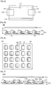
- FIG. 1 is a perspective view showing a light emitting device package according to a first embodiment
- FIG. 2 is a sectional side view of FIG. 1.
- FIG. 3 is a front view of FIG. 1
- FIG. 4 is a bottom view of FIG. 1 .
- the light emitting device package 100 comprises a package body 110 having a light emitting part 114 formed at an oblique angle, lead electrodes 120 and 121, a light emitting device 130, and a resin member 135.
- the package body 110 maybe inject ion-molded by using plastic resin.
- the plastic resin may comprise at least one of polyphthal amide (PPA), polyphenylene sulfide (PPS), polyacryl amide (PAA), and polyether ether ketone (PEEK) .
- the package body 110 can be integrally formed with the lead electrodes 120 and 121 through the injection-molding process. That is, after placing the lead electrodes 120 and 121 in a mold, the plastic resin is poured into the mold, thereby forming the package body 110.
- the package body 110 comprises the light emitting part 114 and a support part 116.
- the light emitting part 114 has a light emitting surface formed at an oblique angle with respect to the support part 116.
- the support part 116 is supported at a rear portion of the light emitting part 114, and a bottom surface 115 of the support part 116 has a flat-surface shape.
- a lower side surface 113 of the light emitting part 114 may be inclined at an oblique angle ⁇ with respect to the bottom surface 115 of the support part 116.
- the oblique angle ⁇ has a range of about 10° to about 80°.
- the bottom surface 115 of the support part 116 of the package body 110 is mounted on a board 150, and the light emitting part 114 of the package body 110 is provided at an oblique angle with respect to the board 150.
- the light emitting part 114 of the package body 110 has a structure in which an upper side surface 112 is parallel to the lower side surface 113, but the structure may be modified.
- a rear surface 117 of the support part 116 may be perpendicular to the bottom surface 115 or inclined with respect to the bottom surface 115.
- the rear surface 117 of the support part 116 protrudes rearward, and such a protrusion structure allows the package body 110 to be balanced when the package body 110 is installed on a planar surface.
- the package body 110 is featured in that the light emitting surface thereof is inclined at an oblique angle. Side surfaces of the package body 110 may be flat, or parallel to their opposite surfaces . In addition, the package body 110 may be bent at a predetermined angle, but the embodiment is not limited thereto.
- the support part 116 of the package body 110 is provided therein with a cavity 111 having a predetermined depth.
- the cavity 111 may have a polygonal surface shape, but this shape may be varied according to molding shapes.
- the cavity 111 can be omitted.
- the embodiment employs the cavity structure for adjusting the amount of emitted light.
- the cavity 111 is formed in the light emitting part 114, and realized as an opening formed at an oblique angle with respect to the bottom surface 115 of the support part 116.
- An inner wall of the cavity 111 maybe perpendicular to the bottom surface 115 or inclined at a predetermined angle with respect to the bottom surface 115.
- the cavity 111 is provided therein with at least one of the lead electrodes 120 and 121.
- the lead electrodes 120 and 121 may be formed by using a lead frame, a metallic layer, or a via structure. According to the embodiment, the lead frame type will be representatively described below.
- First ends of the lead electrodes 120 and 121 are provided in the cavity 111 and second ends 120A and 121A of the lead electrodes 120 and 121 protrude through both sides of the package body 110, respectively.
- the second ends 120A and 121A of the lead electrodes 120 and 121 are disposed and forming with the bottom surface 115 of the support part 116.
- electrodes 124 and 125 provided on the bottom surface 115 of the support part 116 are external electrodes, and bonded with the board 150.
- the lead electrodes 120 and 121 may be subject to a trimming process or/and a forming process for electrical connection with the board 150, and various trimming or forming processes may be performed.
- the lead electrodes 120 and 121 may be attached to the light emitting device 130, and the light emitting device 130 may be connected to the lead electrode 121 through a wire 132.
- the light emitting device 130 may be mounted on the lead electrodes 120 and 121 through a flip scheme.
- the light emitting device 130 may be attached to the lead electrodes 120 and 121 by using a conductive adhesive.
- the light emitting device 130 may be mounted on the lead electrodes 120 and 121 by using at least one wire.
- Such a connection scheme may be varied depending on a chip type and a mounting scheme.
- the light emitting device 130 is provided in the form of a chip.
- the light emitting device 130 is inclined at an oblique angle with respect to a mounting surface of the package body 110.
- the light emitting device 130 may comprise color LED chips such as a blue LED chip, a green LED chip, and a red LED chip or a ultraviolet (UV) LED chip. According to the embodiment, a blue LED chip may be representatively described below.
- At least one light emitting device 130 may be provided in the cavity 111.
- the pattern of the lead electrodes 120 and 121 may be changed.
- the resin member 135 is formed in the cavity 111, and the resin member 135 comprises silicon or epoxy.
- the light emitting device 130 comprises a blue LED chip, a phosphor emitting a yellow light can be added.
- the light emitting device 130 comprises a UV LED chip
- the light emitting device 130 may comprise green, red, and blue phosphors. LED chips and phosphors in the cavity 111 may be variously employed according to a target light of the light emitting device package 100, but the embodiment is not limited thereto.
- the light emitting surface of the light emitting part 114 of the package body 110 is provided at an oblique angle with respect to the bottom surface 115 of the support part 116.
- the light emitting surface of the light emitting part 114 is formed at an oblique angle ⁇ +90° with respect to the bottom surface 115 of the support part 116. Therefore, lights can be emitted from the cavity 111 at an oblique angle. Accordingly, the light emitting device package 100 emits light through the light emitting surface of the package body 110 at an oblique angle direction.
- the light emitting device package 100 emits light at an oblique angle direction with respect to the bottom surface 115.
- the light emitting device package 100 which serves as a light source emitting light at an oblique angle, is applicable to a direct-type light unit or a side-type light unit.
- the light emitting device package 100 may be used with a top view-type package and/or a side-view package in the light unit.
- the light emitting device package 100 can be formed thinner than an existing direct-type package, the light emitting device package 100 is applicable to a slim-type light unit.
- FIG. 5 is a sectional side view showing a light emitting apparatus according to a second embodiment
- FIG. 6 is a plan view showing a light emitting module of FIG. 4 .
- the light emitting apparatus 200 comprises the light emitting module 201 and an optical sheet 210.
- the light emitting module 201 comprises the board 150 and a plurality of light emitting device packages 100.
- the light emitting device package 100 is mounted on the interconnection patterns 155 and 156.
- the light emitting device packages 100 are arrayed on the board 150 in a first direction and/or a second direction in at least one line.
- the light emitting device packages 100 may be arrayed with a constant or random interval.
- the light emitting device packages 100 may be arrayed in the same direction, directions opposite to each other, or directions perpendicular to each other.
- the light emitting device packages 100 may be tilted at a predetermined angle. Such an array direction of the light emitting device packages 100 may be changed for the purpose of light efficiency and light distribution.
- the light emitting device packages 100 may emit lights at the same light emitting angle or different light emitting angles, in which the light emitting angle is within the range of the oblique angle ⁇ (see FIG. 2 ).
- the light emitting angles of the light emitting device packages 100 may be adjusted in a group unit or in a line unit of the light emitting device packages 100 within the range of the oblique angle.
- the light emitting angles of the light emitting device packages 100 between the center portion and the side portion of the board 150 may be the same or different from each other .
- the oblique angle ⁇ may be increased or decreased from the center portion of the board 150 to the side portion of the board 150.
- the light emitting device packages 100 can improve light distribution and light intensity in the board 150 due to characteristics of emitting light at an oblique angle.
- the optical sheet 210 comprises a prism sheet, and the prism sheet may comprise a horizontal prism sheet and/or a vertical prism sheet.
- the optical sheet 210 may comprise a brightness enhancement film. Such an optical sheet may be removed, but the embodiment is not limited thereto.
- a display panel such as an LCD panel may be provided above the optical sheet 210.
- the light emitting device 200 is used as a backlight unit.
- the light emitting device 200 may be provided in a housing. Such components may be added or removed within the scope of the embodiment.
- the light emitting device packages 100 are arrayed in a first direction to irradiate light at an oblique angle, so that uniform light distribution can be achieved. Accordingly, a hot spot can be removed.
- the light emitting device 200 can prevent the hot spot according to the thickness of the light emitting device package 100 and the light emitting direction of the light emitting device package 100. In addition, the light emitting device 200 can reduce a distance from the display panel.
- the light emitting device 200 having such a structure can be provided as a slim light unit than that of an existing light unit, so that the light emitting device 200 can serve as a backlight unit for a notebook computer, a monitor, a terminal, and a TV.
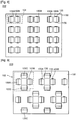
- FIG. 7 is a sectional side view showing a light emitting device 200A according to a third embodiment
- FIG. 8 is a plan view showing a light emitting module 202 of FIG. 7 .
- the light emitting module 202 of the light emitting device 200A has a structure in which a plurality of light emitting device packages 100A and 100B are arrayed according to groups 101.
- the light emitting device packages 100A and 100B in one group 101 may be arrayed at an angle of 180° with respect to each other.
- the groups 101 may be arrayed uniformly or irregularly. Such an array of the groups 101 may be varied according to light distribution and light intensity.
- the light emitting device packages 100A and 100B are arrayed at an angle of 180° with respect to each other in each group 101.
- light emitting angles of the light emitting device packages 100 may gradually increase ( ⁇ 1 > ⁇ 3) or decrease ( ⁇ 1 ⁇ ⁇ 3) from the center portion of the board 120 to the side portion of the board 120.
- the light emitting angles ⁇ 1 and ⁇ 3 are in the range of 10° to 80°. Therefore, the light emitting characteristic of the light emitting device package 100 to emit light at the oblique angle can be used as much as possible.
- FIG. 9 is a plan view showing a light emitting device according to a fourth embodiment.
- a light emitting module 203 of a light emitting device has a structure in which four light emitting device packages 100A, 100B, 100C, and 100D are arrayed in the unit of one group 102.
- the light emitting device packages 100A, 100B, 100C, and 100D are twisted at an angle of about 90° with respect to each other.
- the light emitting device packages 100A, 100B, 100C, and 100D may be arrayed in left, right, up, and down directions.
- the groups 102 of the light emitting device packages 100A, 100B, 100C, and 100D may be arrayed in a zigzag manner.
- the light emitting device packages 100A, 100B, 100C, and 100D can emit light at the oblique angle in each position thereof.
- the light emitting device packages 100A, 100B, 100C, and 100D may have the same light emitting angle or different light emitting angles, in which the light emitting angles are within the range of the oblique angle.
- the light emitting device packages 100A, 100B, 100C, and 100D may be arrayed at a predetermined angle within the range of about 360°.
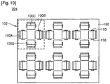
- FIG. 10 is a plan view showing a light emitting device according to a fifth embodiment.
- a light emitting module 204 of a light emitting device has a structure in which four light emitting device packages 100A, 100B, 100C, and 100D are arrayed in the unit of one group 102.
- the light emitting device packages 100A, 100B, 100C, and 100D are twisted at an angle of about 90° with respect to each other.
- the light emitting device packages 100A, 100B, 100C, and 100D may be arrayed in left, right, up, and down directions.
- the groups 102 of the light emitting device packages 100A, 100B, 100C, and 100D may be arrayed in the form of a matrix.
- the light emitting device packages 100A, 100B, 100C, and 100D may be arrayed at a random angle or a constant angle in the range of about 360°.
- the light emitting device packages 100A, 100B, 100C, and 100D of each group 102 can emit light at an oblique angle in each position thereof.
- the light emitting device packages 100A, 100B, 100C, and 100D may emit light at the same light emitting angle or different light emitting angles.
- the light emitting device package emitting light at an oblique angle is applied to the direct-type light unit
- the light emitting device package is applicable to the side-type light unit.
- the light emitting device package emitting light at an oblique angle is applicable to the light unit together with a typical direct-type package, but the embodiments are not limited thereto.
- the light emitting modules 201, 202, 203, and 204 of the light emitting devices may comprise the light emitting device packages in order to prevent a hot spot and irregular brightness distribution.
- the embodiment can provide a light emitting device package capable of emitting light at an oblique angle.
- the embodiment can prevent a hot spot by employing a light emitting device package in a light unit.
- the embodiment can prevent a hot spot by using a light emitting device package capable of emitting light at an oblique angle.
- the embodiment can maintain a uniform color distribution by using a light emitting device package capable of emitting light at an oblique angle.
- the embodiment can improve the light quality of a light unit by employing a light emitting device package in some areas or the whole area of the light unit.
- the LED package can be used as a light source in various fields such as indicators, street lamps, and illumination devices.
- a layer or film when referred to as being 'on' another layer or substrate, it may be directly on other layer or substrate, or intervening layers may also be present. Further, it will be understood that when a layer is referred to as being 'under' another layer, it may be directly under other layer, and one or more intervening layers may also be present. In addition, it will also be understood that when a layer is referred to as being 'between' two layers, it may be the only layer between the two layers, or one or more intervening layers may also be present.
- the LED package can be reliably operated.
- the exemplary embodiments of the present invention have been described, it is understood that the present invention should not be limited to these exemplary embodiments but various changes and modifications can be made by one ordinarily skilled in the art within the spirit and scope of the present invention as hereinafter claimed.
Landscapes
- Led Device Packages (AREA)
Claims (10)
- Lichtemittierendes Bauelementgehäuse, das aufweist:einen Gehäusekörper (110) mit einer lichtemittierenden Fläche, die im Hinblick auf eine Bodenfläche (115) des Gehäusekörpers (110) in einem schiefen Winkel geneigt ist;mehrere Leitungselektroden (120; 121) im Gehäusekörper (110); undmindestens ein lichtemittierendes Bauelement (130), das mit den Leitungselektroden (120; 121) elektrisch verbunden ist,wobeider Gehäusekörper (110) als Einzelmaterialstück ausgebildet ist und ein lichtemittierendes Teil (114) an einer Vorderseite des Gehäusekörpers und ein Stützteil (116) aufweist, das sich vom lichtemittierenden Teil nach hinten erstreckt und das lichtemittierende Teil (114) im Hinblick auf eine Bodenfläche (115) des Stützteils (116) stützt,das lichtemittierende Teil (114) einen Hohlraum (111) in einer lichtemittierenden Fläche (114) davon aufweist, in dem mindestens ein lichtemittierendes Bauelement (130) angeordnet ist,eine Rückfläche (117) des Stützteils (114) vom lichtemittierenden Teil (114) vorsteht,eine Unterseitenfläche (113) des lichtemittierenden Teils (114) im Hinblick auf die Bodenfläche (115) des Stützteils (116) geneigt ist,sich eine Oberseitenfläche (112) des lichtemittierenden Teils (114) von einer Kopffläche des Stützteils (116) erstreckt und im Hinblick darauf geneigt ist,die lichtemittierende Fläche des lichtemittierenden Teils (114) im Hinblick auf die Bodenfläche (115) des Stützteils (116) geneigt ist unddie Bodenfläche (115) des Stützteils (116) und die Kopffläche des Stützteils (116) parallel zueinander sind,wobei die lichtemittierende Fläche des Gehäusekörpers (110) in einem Winkel in einem Bereich von 10° bis 80° im Hinblick auf die Bodenfläche (115) des Stützteils (116) geneigt ist, wobei der Winkel außen am Gehäusekörper gemessen wird, wobei ein oberer Abschnitt der Rückfläche (117) des Stützteils (116) des Gehäusekörpers (110) über einen unteren Abschnitt der Rückfläche des Stützteils hinaus nach hinten vorsteht, wobei der obere Abschnitt nicht senkrecht zur Bodenfläche (115) des Stützteils geneigt ist, so dass das lichtemittierende Bauelementgehäuse ausbalanciert ist, wenn der Gehäusekörper (110) auf einer ebenen Oberfläche über die Bodenfläche des Stützteils angebaut ist.
- Lichtemittierendes Bauelementgehäuse nach Anspruch 1, wobei die Unterseitenfläche (113) des lichtemittierenden Teils (116) und die Oberseitenfläche (112) des lichtemittierenden Teils (116) parallel zueinander sind.
- Lichtemittierendes Bauelementgehäuse nach Anspruch 1 oder Anspruch 2, wobei ein erstes Ende jeder Leitungselektrode (120; 121) durch einen Außenabschnitt des Gehäusekörpers (111) auf der Bodenfläche (115) vorgesehen ist.
- Lichtemittierendes Bauelementgehäuse nach einem der Ansprüche 1 bis 3, wobei der Hohlraum (111) eine Innenwand hat, die senkrecht zu einer Bodenfläche des Hohlraums (111) oder im Hinblick auf die Bodenfläche des Hohlraums (111) nach außen geneigt ist.
- Lichtemittierendes Bauelementgehäuse nach einem der Ansprüche 1 bis 4, wobei der Gehäusekörper (110) ein Kunstharzmaterial (135) aufweist und jede Leitungselektrode (120; 121) einen Leitungsrahmen aufweist.
- Lichtemittierendes Bauelementgehäuse nach einem der Ansprüche 1 bis 5, wobei der Gehäusekörper (110) ein Material aufweist, das aus der Gruppe ausgewählt ist, die aus Polyphthalamid (PPA), Polyphenylensulfid (PPS), Polyacrylamid (PAA) und Polyetherketon (PEEK) besteht.
- Lichtemittierendes Bauelementgehäuse nach einem der Ansprüche 1 bis 6, wobei der Hohlraum (111) ein transparentes Harzbauteil oder ein transparentes Leuchtstoff-Harzbauteil aufweist und
wobei das lichtemittierende Bauelement (130) eine Farb-LED, die einen blauen, einen grünen und einen roten LED-Chip aufweist, und/oder einen UV-LED-Chip aufweist. - Lichtemittierende Vorrichtung, die aufweist:eine Platine (150) mit einer Verbindungsstruktur (155; 156); undmehrere lichtemittierende Bauelementgehäuse (100) nach einem der Ansprüche 1 bis 9 und mit einer lichtemittierenden Fläche, die im Hinblick auf eine Kopffläche zur Platine (150) in einem schiefen Winkel geneigt ist.
- Lichtemittierende Vorrichtung nach Anspruch 8, wobei die lichtemittierenden Bauelementgehäuse (100) in gleicher Richtung oder unterschiedlichen Richtungen angeordnet sind.
- Lichtemittierende Vorrichtung nach Anspruch 8 oder Anspruch 9, wobei die lichtemittierenden Bauelementgehäuse (100) in einem vorbestimmten Winkel im Hinblick aufeinander verdreht sind.
Applications Claiming Priority (2)
| Application Number | Priority Date | Filing Date | Title |
|---|---|---|---|
| KR20080101641A KR101509760B1 (ko) | 2008-10-16 | 2008-10-16 | 발광 다이오드 패키지 및 그 제조방법, 이를 구비한 발광 장치 |
| PCT/KR2009/005235 WO2010044548A2 (ko) | 2008-10-16 | 2009-09-15 | 발광 소자 패키지 및 그 제조방법, 발광 장치 |
Publications (3)
| Publication Number | Publication Date |
|---|---|
| EP2249407A2 EP2249407A2 (de) | 2010-11-10 |
| EP2249407A4 EP2249407A4 (de) | 2014-06-25 |
| EP2249407B1 true EP2249407B1 (de) | 2020-04-22 |
Family
ID=42107007
Family Applications (1)
| Application Number | Title | Priority Date | Filing Date |
|---|---|---|---|
| EP09820698.0A Active EP2249407B1 (de) | 2008-10-16 | 2009-09-15 | Gehäuse mit lichtemittierender vorrichtung, dessen herstellungsverfahren und beleuchtungsvorrichtung |
Country Status (6)
| Country | Link |
|---|---|
| US (1) | US8618558B2 (de) |
| EP (1) | EP2249407B1 (de) |
| JP (1) | JP5512689B2 (de) |
| KR (1) | KR101509760B1 (de) |
| CN (1) | CN101981714B (de) |
| WO (1) | WO2010044548A2 (de) |
Families Citing this family (13)
| Publication number | Priority date | Publication date | Assignee | Title |
|---|---|---|---|---|
| TW201020643A (en) * | 2008-11-25 | 2010-06-01 | Chi Mei Lighting Tech Corp | Side view type light-emitting diode package structure, and manufacturing method and application thereof |
| JP6113420B2 (ja) * | 2011-05-30 | 2017-04-12 | 日亜化学工業株式会社 | 発光装置 |
| KR101813495B1 (ko) * | 2011-06-08 | 2017-12-29 | 엘지이노텍 주식회사 | 발광소자 패키지 |
| CN102496613A (zh) * | 2011-12-14 | 2012-06-13 | 南京中电熊猫液晶显示科技有限公司 | Led封装和包括该led封装的背光模组 |
| TWD161897S (zh) * | 2013-02-08 | 2014-07-21 | 晶元光電股份有限公司 | 發光二極體之部分 |
| USD847102S1 (en) | 2013-02-08 | 2019-04-30 | Epistar Corporation | Light emitting diode |
| JP6318844B2 (ja) * | 2014-05-20 | 2018-05-09 | 日亜化学工業株式会社 | 発光装置 |
| CN105761624B (zh) * | 2016-01-19 | 2019-03-15 | 潘尚法 | 一种带倾角的led元件、led灯条和显示屏 |
| CN108565326A (zh) * | 2018-02-09 | 2018-09-21 | 佛山市国星光电股份有限公司 | Led支架、led器件和led显示屏 |
| US20190331965A1 (en) * | 2018-04-26 | 2019-10-31 | Wuhan China Star Optoelectronics Technology Co., Ltd. | Light source module, backlight module, and lcd device |
| CN113451487B (zh) * | 2020-08-20 | 2022-09-23 | 重庆康佳光电技术研究院有限公司 | 显示面板及具有其的显示装置 |
| EP4425583A4 (de) * | 2021-10-26 | 2025-11-05 | Lg Electronics Inc | Anzeigevorrichtung mit lichtemittierendem halbleiterelement |
| CN115621396A (zh) * | 2022-10-31 | 2023-01-17 | 佛山市国星光电股份有限公司 | 斜面发光灯珠及其支架、制作方法和显示装置 |
Citations (1)
| Publication number | Priority date | Publication date | Assignee | Title |
|---|---|---|---|---|
| KR100820529B1 (ko) * | 2006-05-11 | 2008-04-08 | 엘지이노텍 주식회사 | 발광 장치 및 그 제조방법, 면 발광 장치 |
Family Cites Families (18)
| Publication number | Priority date | Publication date | Assignee | Title |
|---|---|---|---|---|
| JPS6441907U (de) | 1987-09-08 | 1989-03-13 | ||
| JP2605856Y2 (ja) | 1993-01-12 | 2000-08-21 | 株式会社シチズン電子 | 発光ダイオード |
| JP3704794B2 (ja) | 1996-04-12 | 2005-10-12 | 日亜化学工業株式会社 | Led表示器の形成方法 |
| CA2232843C (en) * | 1997-03-25 | 2002-03-12 | Koichi Haruta | Plastic package, semiconductor device, and method of manufacturing plastic package |
| US6469322B1 (en) * | 1998-02-06 | 2002-10-22 | General Electric Company | Green emitting phosphor for use in UV light emitting diodes |
| JP3495923B2 (ja) * | 1998-09-09 | 2004-02-09 | シャープ株式会社 | 通信用光学素子組立体 |
| US6257746B1 (en) * | 1998-11-03 | 2001-07-10 | K. W. Muth Company, Inc. | Signalling assembly |
| JP2001053294A (ja) | 1999-08-04 | 2001-02-23 | Hamamatsu Photonics Kk | 投受光装置 |
| JP2002270902A (ja) | 2001-03-07 | 2002-09-20 | Toyoda Gosei Co Ltd | 発光ダイオード |
| JP2003264299A (ja) | 2002-03-11 | 2003-09-19 | Honda Motor Co Ltd | 受光装置、発光装置及び光無線通信装置 |
| JP4046229B2 (ja) * | 2003-08-01 | 2008-02-13 | シーシーエス株式会社 | 光照射装置及び光照射システム |
| KR100580765B1 (ko) * | 2003-09-22 | 2006-05-15 | 엘지이노텍 주식회사 | 발광 다이오드 패키지 및 그 제조방법 |
| JP2005128236A (ja) * | 2003-10-23 | 2005-05-19 | Seiko Epson Corp | 光源装置、照明装置及びプロジェクタ |
| KR100565842B1 (ko) * | 2004-03-30 | 2006-03-30 | 서울반도체 주식회사 | 방사각이 지향된 발광다이오드 |
| JP5122062B2 (ja) | 2004-09-22 | 2013-01-16 | 株式会社光波 | 発光装置 |
| WO2007075143A1 (en) * | 2005-12-29 | 2007-07-05 | Lam Chiang Lim | High power led housing removably fixed to a heat sink |
| CN100557832C (zh) | 2006-02-15 | 2009-11-04 | 苑宝义 | 路灯专用功率型发光二极管 |
| KR101261881B1 (ko) * | 2006-06-09 | 2013-05-06 | 엘지디스플레이 주식회사 | 발광다이오드 어셈블리 및 이를 포함하는 액정표시장치모듈 |
-
2008
- 2008-10-16 KR KR20080101641A patent/KR101509760B1/ko not_active Expired - Fee Related
-
2009
- 2009-09-15 WO PCT/KR2009/005235 patent/WO2010044548A2/ko not_active Ceased
- 2009-09-15 CN CN200980110795.9A patent/CN101981714B/zh not_active Expired - Fee Related
- 2009-09-15 JP JP2011532010A patent/JP5512689B2/ja not_active Expired - Fee Related
- 2009-09-15 EP EP09820698.0A patent/EP2249407B1/de active Active
- 2009-09-15 US US12/559,814 patent/US8618558B2/en not_active Expired - Fee Related
Patent Citations (1)
| Publication number | Priority date | Publication date | Assignee | Title |
|---|---|---|---|---|
| KR100820529B1 (ko) * | 2006-05-11 | 2008-04-08 | 엘지이노텍 주식회사 | 발광 장치 및 그 제조방법, 면 발광 장치 |
Also Published As
| Publication number | Publication date |
|---|---|
| JP5512689B2 (ja) | 2014-06-04 |
| KR101509760B1 (ko) | 2015-04-08 |
| WO2010044548A2 (ko) | 2010-04-22 |
| EP2249407A4 (de) | 2014-06-25 |
| CN101981714B (zh) | 2014-05-07 |
| JP2012506142A (ja) | 2012-03-08 |
| US20100096644A1 (en) | 2010-04-22 |
| WO2010044548A3 (ko) | 2010-07-01 |
| EP2249407A2 (de) | 2010-11-10 |
| CN101981714A (zh) | 2011-02-23 |
| KR20100050590A (ko) | 2010-05-14 |
| US8618558B2 (en) | 2013-12-31 |
Similar Documents
| Publication | Publication Date | Title |
|---|---|---|
| EP2249407B1 (de) | Gehäuse mit lichtemittierender vorrichtung, dessen herstellungsverfahren und beleuchtungsvorrichtung | |
| US9564567B2 (en) | Light emitting device package and method of fabricating the same | |
| US7997749B2 (en) | Light emitting module and light unit having the same | |
| US9705054B2 (en) | Light emitting device module | |
| US8545082B2 (en) | Light emitting apparatus and lighting system | |
| US8530918B2 (en) | Light emitting device package and lighting system | |
| US8704263B2 (en) | Light emitting apparatus with an opening part, manufacturing method thereof, and light unit | |
| US10566508B2 (en) | Molded surface mount device LED display module | |
| US8476662B2 (en) | Light emitting device, method for manufacturing the same, and backlight unit | |
| US20120074456A1 (en) | Light emitting device package | |
| US20150198294A1 (en) | Light bar, backlight device, and manufacturing methods thereof | |
| KR20110139453A (ko) | 발광 장치 및 조명 시스템 | |
| KR101370790B1 (ko) | 발광 장치 | |
| KR101370791B1 (ko) | 발광 장치 | |
| KR101676670B1 (ko) | 발광 소자 | |
| KR101735310B1 (ko) | 발광소자 패키지 |
Legal Events
| Date | Code | Title | Description |
|---|---|---|---|
| PUAI | Public reference made under article 153(3) epc to a published international application that has entered the european phase |
Free format text: ORIGINAL CODE: 0009012 |
|
| 17P | Request for examination filed |
Effective date: 20100826 |
|
| AK | Designated contracting states |
Kind code of ref document: A2 Designated state(s): AT BE BG CH CY CZ DE DK EE ES FI FR GB GR HR HU IE IS IT LI LT LU LV MC MK MT NL NO PL PT RO SE SI SK SM TR |
|
| AX | Request for extension of the european patent |
Extension state: AL BA RS |
|
| DAX | Request for extension of the european patent (deleted) | ||
| RAP1 | Party data changed (applicant data changed or rights of an application transferred) |
Owner name: LG INNOTEK CO., LTD. |
|
| A4 | Supplementary search report drawn up and despatched |
Effective date: 20140526 |
|
| RIC1 | Information provided on ipc code assigned before grant |
Ipc: H01L 33/48 20100101AFI20140520BHEP |
|
| RAP1 | Party data changed (applicant data changed or rights of an application transferred) |
Owner name: LG INNOTEK CO., LTD. |
|
| STAA | Information on the status of an ep patent application or granted ep patent |
Free format text: STATUS: EXAMINATION IS IN PROGRESS |
|
| 17Q | First examination report despatched |
Effective date: 20190107 |
|
| GRAP | Despatch of communication of intention to grant a patent |
Free format text: ORIGINAL CODE: EPIDOSNIGR1 |
|
| STAA | Information on the status of an ep patent application or granted ep patent |
Free format text: STATUS: GRANT OF PATENT IS INTENDED |
|
| INTG | Intention to grant announced |
Effective date: 20191210 |
|
| GRAS | Grant fee paid |
Free format text: ORIGINAL CODE: EPIDOSNIGR3 |
|
| GRAA | (expected) grant |
Free format text: ORIGINAL CODE: 0009210 |
|
| STAA | Information on the status of an ep patent application or granted ep patent |
Free format text: STATUS: THE PATENT HAS BEEN GRANTED |
|
| AK | Designated contracting states |
Kind code of ref document: B1 Designated state(s): AT BE BG CH CY CZ DE DK EE ES FI FR GB GR HR HU IE IS IT LI LT LU LV MC MK MT NL NO PL PT RO SE SI SK SM TR |
|
| REG | Reference to a national code |
Ref country code: GB Ref legal event code: FG4D |
|
| REG | Reference to a national code |
Ref country code: CH Ref legal event code: EP |
|
| REG | Reference to a national code |
Ref country code: IE Ref legal event code: FG4D |
|
| REG | Reference to a national code |
Ref country code: DE Ref legal event code: R096 Ref document number: 602009061823 Country of ref document: DE |
|
| REG | Reference to a national code |
Ref country code: AT Ref legal event code: REF Ref document number: 1261296 Country of ref document: AT Kind code of ref document: T Effective date: 20200515 |
|
| REG | Reference to a national code |
Ref country code: LT Ref legal event code: MG4D |
|
| REG | Reference to a national code |
Ref country code: NL Ref legal event code: MP Effective date: 20200422 |
|
| PG25 | Lapsed in a contracting state [announced via postgrant information from national office to epo] |
Ref country code: NO Free format text: LAPSE BECAUSE OF FAILURE TO SUBMIT A TRANSLATION OF THE DESCRIPTION OR TO PAY THE FEE WITHIN THE PRESCRIBED TIME-LIMIT Effective date: 20200722 Ref country code: IS Free format text: LAPSE BECAUSE OF FAILURE TO SUBMIT A TRANSLATION OF THE DESCRIPTION OR TO PAY THE FEE WITHIN THE PRESCRIBED TIME-LIMIT Effective date: 20200822 Ref country code: GR Free format text: LAPSE BECAUSE OF FAILURE TO SUBMIT A TRANSLATION OF THE DESCRIPTION OR TO PAY THE FEE WITHIN THE PRESCRIBED TIME-LIMIT Effective date: 20200723 Ref country code: LT Free format text: LAPSE BECAUSE OF FAILURE TO SUBMIT A TRANSLATION OF THE DESCRIPTION OR TO PAY THE FEE WITHIN THE PRESCRIBED TIME-LIMIT Effective date: 20200422 Ref country code: PT Free format text: LAPSE BECAUSE OF FAILURE TO SUBMIT A TRANSLATION OF THE DESCRIPTION OR TO PAY THE FEE WITHIN THE PRESCRIBED TIME-LIMIT Effective date: 20200824 Ref country code: NL Free format text: LAPSE BECAUSE OF FAILURE TO SUBMIT A TRANSLATION OF THE DESCRIPTION OR TO PAY THE FEE WITHIN THE PRESCRIBED TIME-LIMIT Effective date: 20200422 Ref country code: SE Free format text: LAPSE BECAUSE OF FAILURE TO SUBMIT A TRANSLATION OF THE DESCRIPTION OR TO PAY THE FEE WITHIN THE PRESCRIBED TIME-LIMIT Effective date: 20200422 Ref country code: FI Free format text: LAPSE BECAUSE OF FAILURE TO SUBMIT A TRANSLATION OF THE DESCRIPTION OR TO PAY THE FEE WITHIN THE PRESCRIBED TIME-LIMIT Effective date: 20200422 |
|
| REG | Reference to a national code |
Ref country code: AT Ref legal event code: MK05 Ref document number: 1261296 Country of ref document: AT Kind code of ref document: T Effective date: 20200422 |
|
| PG25 | Lapsed in a contracting state [announced via postgrant information from national office to epo] |
Ref country code: BG Free format text: LAPSE BECAUSE OF FAILURE TO SUBMIT A TRANSLATION OF THE DESCRIPTION OR TO PAY THE FEE WITHIN THE PRESCRIBED TIME-LIMIT Effective date: 20200722 Ref country code: HR Free format text: LAPSE BECAUSE OF FAILURE TO SUBMIT A TRANSLATION OF THE DESCRIPTION OR TO PAY THE FEE WITHIN THE PRESCRIBED TIME-LIMIT Effective date: 20200422 Ref country code: LV Free format text: LAPSE BECAUSE OF FAILURE TO SUBMIT A TRANSLATION OF THE DESCRIPTION OR TO PAY THE FEE WITHIN THE PRESCRIBED TIME-LIMIT Effective date: 20200422 |
|
| REG | Reference to a national code |
Ref country code: DE Ref legal event code: R097 Ref document number: 602009061823 Country of ref document: DE |
|
| PG25 | Lapsed in a contracting state [announced via postgrant information from national office to epo] |
Ref country code: AT Free format text: LAPSE BECAUSE OF FAILURE TO SUBMIT A TRANSLATION OF THE DESCRIPTION OR TO PAY THE FEE WITHIN THE PRESCRIBED TIME-LIMIT Effective date: 20200422 Ref country code: CZ Free format text: LAPSE BECAUSE OF FAILURE TO SUBMIT A TRANSLATION OF THE DESCRIPTION OR TO PAY THE FEE WITHIN THE PRESCRIBED TIME-LIMIT Effective date: 20200422 Ref country code: ES Free format text: LAPSE BECAUSE OF FAILURE TO SUBMIT A TRANSLATION OF THE DESCRIPTION OR TO PAY THE FEE WITHIN THE PRESCRIBED TIME-LIMIT Effective date: 20200422 Ref country code: RO Free format text: LAPSE BECAUSE OF FAILURE TO SUBMIT A TRANSLATION OF THE DESCRIPTION OR TO PAY THE FEE WITHIN THE PRESCRIBED TIME-LIMIT Effective date: 20200422 Ref country code: IT Free format text: LAPSE BECAUSE OF FAILURE TO SUBMIT A TRANSLATION OF THE DESCRIPTION OR TO PAY THE FEE WITHIN THE PRESCRIBED TIME-LIMIT Effective date: 20200422 Ref country code: EE Free format text: LAPSE BECAUSE OF FAILURE TO SUBMIT A TRANSLATION OF THE DESCRIPTION OR TO PAY THE FEE WITHIN THE PRESCRIBED TIME-LIMIT Effective date: 20200422 Ref country code: SM Free format text: LAPSE BECAUSE OF FAILURE TO SUBMIT A TRANSLATION OF THE DESCRIPTION OR TO PAY THE FEE WITHIN THE PRESCRIBED TIME-LIMIT Effective date: 20200422 Ref country code: DK Free format text: LAPSE BECAUSE OF FAILURE TO SUBMIT A TRANSLATION OF THE DESCRIPTION OR TO PAY THE FEE WITHIN THE PRESCRIBED TIME-LIMIT Effective date: 20200422 |
|
| PG25 | Lapsed in a contracting state [announced via postgrant information from national office to epo] |
Ref country code: SK Free format text: LAPSE BECAUSE OF FAILURE TO SUBMIT A TRANSLATION OF THE DESCRIPTION OR TO PAY THE FEE WITHIN THE PRESCRIBED TIME-LIMIT Effective date: 20200422 Ref country code: PL Free format text: LAPSE BECAUSE OF FAILURE TO SUBMIT A TRANSLATION OF THE DESCRIPTION OR TO PAY THE FEE WITHIN THE PRESCRIBED TIME-LIMIT Effective date: 20200422 |
|
| PLBE | No opposition filed within time limit |
Free format text: ORIGINAL CODE: 0009261 |
|
| STAA | Information on the status of an ep patent application or granted ep patent |
Free format text: STATUS: NO OPPOSITION FILED WITHIN TIME LIMIT |
|
| 26N | No opposition filed |
Effective date: 20210125 |
|
| PG25 | Lapsed in a contracting state [announced via postgrant information from national office to epo] |
Ref country code: MC Free format text: LAPSE BECAUSE OF FAILURE TO SUBMIT A TRANSLATION OF THE DESCRIPTION OR TO PAY THE FEE WITHIN THE PRESCRIBED TIME-LIMIT Effective date: 20200422 |
|
| REG | Reference to a national code |
Ref country code: CH Ref legal event code: PL |
|
| GBPC | Gb: european patent ceased through non-payment of renewal fee |
Effective date: 20200915 |
|
| PG25 | Lapsed in a contracting state [announced via postgrant information from national office to epo] |
Ref country code: SI Free format text: LAPSE BECAUSE OF FAILURE TO SUBMIT A TRANSLATION OF THE DESCRIPTION OR TO PAY THE FEE WITHIN THE PRESCRIBED TIME-LIMIT Effective date: 20200422 |
|
| REG | Reference to a national code |
Ref country code: BE Ref legal event code: MM Effective date: 20200930 |
|
| PG25 | Lapsed in a contracting state [announced via postgrant information from national office to epo] |
Ref country code: LU Free format text: LAPSE BECAUSE OF NON-PAYMENT OF DUE FEES Effective date: 20200915 |
|
| PG25 | Lapsed in a contracting state [announced via postgrant information from national office to epo] |
Ref country code: FR Free format text: LAPSE BECAUSE OF NON-PAYMENT OF DUE FEES Effective date: 20200930 |
|
| PG25 | Lapsed in a contracting state [announced via postgrant information from national office to epo] |
Ref country code: BE Free format text: LAPSE BECAUSE OF NON-PAYMENT OF DUE FEES Effective date: 20200930 Ref country code: CH Free format text: LAPSE BECAUSE OF NON-PAYMENT OF DUE FEES Effective date: 20200930 Ref country code: GB Free format text: LAPSE BECAUSE OF NON-PAYMENT OF DUE FEES Effective date: 20200915 Ref country code: LI Free format text: LAPSE BECAUSE OF NON-PAYMENT OF DUE FEES Effective date: 20200930 Ref country code: IE Free format text: LAPSE BECAUSE OF NON-PAYMENT OF DUE FEES Effective date: 20200915 |
|
| REG | Reference to a national code |
Ref country code: DE Ref legal event code: R081 Ref document number: 602009061823 Country of ref document: DE Owner name: SUZHOU LEKIN SEMICONDUCTOR CO. LTD., TAICANG, CN Free format text: FORMER OWNER: LG INNOTEK CO., LTD., SEOUL, KR |
|
| PG25 | Lapsed in a contracting state [announced via postgrant information from national office to epo] |
Ref country code: TR Free format text: LAPSE BECAUSE OF FAILURE TO SUBMIT A TRANSLATION OF THE DESCRIPTION OR TO PAY THE FEE WITHIN THE PRESCRIBED TIME-LIMIT Effective date: 20200422 Ref country code: MT Free format text: LAPSE BECAUSE OF FAILURE TO SUBMIT A TRANSLATION OF THE DESCRIPTION OR TO PAY THE FEE WITHIN THE PRESCRIBED TIME-LIMIT Effective date: 20200422 Ref country code: CY Free format text: LAPSE BECAUSE OF FAILURE TO SUBMIT A TRANSLATION OF THE DESCRIPTION OR TO PAY THE FEE WITHIN THE PRESCRIBED TIME-LIMIT Effective date: 20200422 |
|
| PG25 | Lapsed in a contracting state [announced via postgrant information from national office to epo] |
Ref country code: MK Free format text: LAPSE BECAUSE OF FAILURE TO SUBMIT A TRANSLATION OF THE DESCRIPTION OR TO PAY THE FEE WITHIN THE PRESCRIBED TIME-LIMIT Effective date: 20200422 |
|
| PGFP | Annual fee paid to national office [announced via postgrant information from national office to epo] |
Ref country code: DE Payment date: 20230808 Year of fee payment: 15 |
|
| REG | Reference to a national code |
Ref country code: DE Ref legal event code: R079 Ref document number: 602009061823 Country of ref document: DE Free format text: PREVIOUS MAIN CLASS: H01L0033480000 Ipc: H10H0020850000 |
|
| REG | Reference to a national code |
Ref country code: DE Ref legal event code: R119 Ref document number: 602009061823 Country of ref document: DE |
|
| PG25 | Lapsed in a contracting state [announced via postgrant information from national office to epo] |
Ref country code: DE Free format text: LAPSE BECAUSE OF NON-PAYMENT OF DUE FEES Effective date: 20250401 |