EP2248191B1 - Diode électroluminescente à semi-conducteur et procédé de fabrication d'une diode à semi-conducteur - Google Patents
Diode électroluminescente à semi-conducteur et procédé de fabrication d'une diode à semi-conducteur Download PDFInfo
- Publication number
- EP2248191B1 EP2248191B1 EP09714695.5A EP09714695A EP2248191B1 EP 2248191 B1 EP2248191 B1 EP 2248191B1 EP 09714695 A EP09714695 A EP 09714695A EP 2248191 B1 EP2248191 B1 EP 2248191B1
- Authority
- EP
- European Patent Office
- Prior art keywords
- layer
- emitting diode
- light
- doped
- oxide
- Prior art date
- Legal status (The legal status is an assumption and is not a legal conclusion. Google has not performed a legal analysis and makes no representation as to the accuracy of the status listed.)
- Active
Links
- 239000004065 semiconductor Substances 0.000 title claims description 129
- 238000004519 manufacturing process Methods 0.000 title claims description 6
- 238000004544 sputter deposition Methods 0.000 claims description 23
- 239000002019 doping agent Substances 0.000 claims description 19
- 239000000463 material Substances 0.000 claims description 18
- 238000000151 deposition Methods 0.000 claims description 13
- 238000000034 method Methods 0.000 claims description 13
- XLOMVQKBTHCTTD-UHFFFAOYSA-N Zinc monoxide Chemical compound [Zn]=O XLOMVQKBTHCTTD-UHFFFAOYSA-N 0.000 claims description 8
- 230000008021 deposition Effects 0.000 claims description 6
- 239000011787 zinc oxide Substances 0.000 claims description 4
- 238000005530 etching Methods 0.000 claims description 3
- AMGQUBHHOARCQH-UHFFFAOYSA-N indium;oxotin Chemical compound [In].[Sn]=O AMGQUBHHOARCQH-UHFFFAOYSA-N 0.000 claims description 3
- YVTHLONGBIQYBO-UHFFFAOYSA-N zinc indium(3+) oxygen(2-) Chemical compound [O--].[Zn++].[In+3] YVTHLONGBIQYBO-UHFFFAOYSA-N 0.000 claims description 3
- 230000005855 radiation Effects 0.000 description 13
- 230000005670 electromagnetic radiation Effects 0.000 description 11
- 239000000758 substrate Substances 0.000 description 6
- 229910052782 aluminium Inorganic materials 0.000 description 5
- XAGFODPZIPBFFR-UHFFFAOYSA-N aluminium Chemical compound [Al] XAGFODPZIPBFFR-UHFFFAOYSA-N 0.000 description 5
- 238000011161 development Methods 0.000 description 5
- 229910002601 GaN Inorganic materials 0.000 description 4
- 238000005229 chemical vapour deposition Methods 0.000 description 4
- JMASRVWKEDWRBT-UHFFFAOYSA-N Gallium nitride Chemical compound [Ga]#N JMASRVWKEDWRBT-UHFFFAOYSA-N 0.000 description 3
- XUIMIQQOPSSXEZ-UHFFFAOYSA-N Silicon Chemical compound [Si] XUIMIQQOPSSXEZ-UHFFFAOYSA-N 0.000 description 3
- 239000013078 crystal Substances 0.000 description 3
- PCHJSUWPFVWCPO-UHFFFAOYSA-N gold Chemical compound [Au] PCHJSUWPFVWCPO-UHFFFAOYSA-N 0.000 description 3
- 229910052737 gold Inorganic materials 0.000 description 3
- 239000010931 gold Substances 0.000 description 3
- 238000002310 reflectometry Methods 0.000 description 3
- 239000010703 silicon Substances 0.000 description 3
- 229910052710 silicon Inorganic materials 0.000 description 3
- 229910052709 silver Inorganic materials 0.000 description 3
- 239000004332 silver Substances 0.000 description 3
- 238000003892 spreading Methods 0.000 description 3
- IJGRMHOSHXDMSA-UHFFFAOYSA-N Atomic nitrogen Chemical compound N#N IJGRMHOSHXDMSA-UHFFFAOYSA-N 0.000 description 2
- GYHNNYVSQQEPJS-UHFFFAOYSA-N Gallium Chemical compound [Ga] GYHNNYVSQQEPJS-UHFFFAOYSA-N 0.000 description 2
- FYYHWMGAXLPEAU-UHFFFAOYSA-N Magnesium Chemical compound [Mg] FYYHWMGAXLPEAU-UHFFFAOYSA-N 0.000 description 2
- VYPSYNLAJGMNEJ-UHFFFAOYSA-N Silicium dioxide Chemical compound O=[Si]=O VYPSYNLAJGMNEJ-UHFFFAOYSA-N 0.000 description 2
- BQCADISMDOOEFD-UHFFFAOYSA-N Silver Chemical compound [Ag] BQCADISMDOOEFD-UHFFFAOYSA-N 0.000 description 2
- 230000002411 adverse Effects 0.000 description 2
- 229910052733 gallium Inorganic materials 0.000 description 2
- 229910052738 indium Inorganic materials 0.000 description 2
- APFVFJFRJDLVQX-UHFFFAOYSA-N indium atom Chemical compound [In] APFVFJFRJDLVQX-UHFFFAOYSA-N 0.000 description 2
- 229910052749 magnesium Inorganic materials 0.000 description 2
- 239000011777 magnesium Substances 0.000 description 2
- 229910052751 metal Inorganic materials 0.000 description 2
- 239000002184 metal Substances 0.000 description 2
- 238000001451 molecular beam epitaxy Methods 0.000 description 2
- 238000005240 physical vapour deposition Methods 0.000 description 2
- 238000000623 plasma-assisted chemical vapour deposition Methods 0.000 description 2
- 229910052814 silicon oxide Inorganic materials 0.000 description 2
- 238000012935 Averaging Methods 0.000 description 1
- 229910000530 Gallium indium arsenide Inorganic materials 0.000 description 1
- OAICVXFJPJFONN-UHFFFAOYSA-N Phosphorus Chemical compound [P] OAICVXFJPJFONN-UHFFFAOYSA-N 0.000 description 1
- 229910052581 Si3N4 Inorganic materials 0.000 description 1
- KXNLCSXBJCPWGL-UHFFFAOYSA-N [Ga].[As].[In] Chemical compound [Ga].[As].[In] KXNLCSXBJCPWGL-UHFFFAOYSA-N 0.000 description 1
- 229910045601 alloy Inorganic materials 0.000 description 1
- 239000000956 alloy Substances 0.000 description 1
- RNQKDQAVIXDKAG-UHFFFAOYSA-N aluminum gallium Chemical compound [Al].[Ga] RNQKDQAVIXDKAG-UHFFFAOYSA-N 0.000 description 1
- AJGDITRVXRPLBY-UHFFFAOYSA-N aluminum indium Chemical compound [Al].[In] AJGDITRVXRPLBY-UHFFFAOYSA-N 0.000 description 1
- 229910052785 arsenic Inorganic materials 0.000 description 1
- RQNWIZPPADIBDY-UHFFFAOYSA-N arsenic atom Chemical compound [As] RQNWIZPPADIBDY-UHFFFAOYSA-N 0.000 description 1
- 230000015572 biosynthetic process Effects 0.000 description 1
- 230000001143 conditioned effect Effects 0.000 description 1
- 238000010276 construction Methods 0.000 description 1
- PMHQVHHXPFUNSP-UHFFFAOYSA-M copper(1+);methylsulfanylmethane;bromide Chemical compound Br[Cu].CSC PMHQVHHXPFUNSP-UHFFFAOYSA-M 0.000 description 1
- 238000005137 deposition process Methods 0.000 description 1
- 238000009826 distribution Methods 0.000 description 1
- 230000000694 effects Effects 0.000 description 1
- 238000010292 electrical insulation Methods 0.000 description 1
- 239000011521 glass Substances 0.000 description 1
- 238000010884 ion-beam technique Methods 0.000 description 1
- 229910001092 metal group alloy Inorganic materials 0.000 description 1
- 150000002739 metals Chemical class 0.000 description 1
- 238000013508 migration Methods 0.000 description 1
- 230000005012 migration Effects 0.000 description 1
- 239000000203 mixture Substances 0.000 description 1
- 229910052757 nitrogen Inorganic materials 0.000 description 1
- 230000003287 optical effect Effects 0.000 description 1
- 230000005693 optoelectronics Effects 0.000 description 1
- 229910052698 phosphorus Inorganic materials 0.000 description 1
- 239000011574 phosphorus Substances 0.000 description 1
- HQVNEWCFYHHQES-UHFFFAOYSA-N silicon nitride Chemical compound N12[Si]34N5[Si]62N3[Si]51N64 HQVNEWCFYHHQES-UHFFFAOYSA-N 0.000 description 1
- 238000002207 thermal evaporation Methods 0.000 description 1
- 239000010409 thin film Substances 0.000 description 1
- 230000007704 transition Effects 0.000 description 1
Images


Classifications
-
- H—ELECTRICITY
- H01—ELECTRIC ELEMENTS
- H01L—SEMICONDUCTOR DEVICES NOT COVERED BY CLASS H10
- H01L33/00—Semiconductor devices with at least one potential-jump barrier or surface barrier specially adapted for light emission; Processes or apparatus specially adapted for the manufacture or treatment thereof or of parts thereof; Details thereof
- H01L33/36—Semiconductor devices with at least one potential-jump barrier or surface barrier specially adapted for light emission; Processes or apparatus specially adapted for the manufacture or treatment thereof or of parts thereof; Details thereof characterised by the electrodes
- H01L33/40—Materials therefor
- H01L33/405—Reflective materials
-
- H—ELECTRICITY
- H01—ELECTRIC ELEMENTS
- H01L—SEMICONDUCTOR DEVICES NOT COVERED BY CLASS H10
- H01L33/00—Semiconductor devices with at least one potential-jump barrier or surface barrier specially adapted for light emission; Processes or apparatus specially adapted for the manufacture or treatment thereof or of parts thereof; Details thereof
- H01L33/02—Semiconductor devices with at least one potential-jump barrier or surface barrier specially adapted for light emission; Processes or apparatus specially adapted for the manufacture or treatment thereof or of parts thereof; Details thereof characterised by the semiconductor bodies
- H01L33/20—Semiconductor devices with at least one potential-jump barrier or surface barrier specially adapted for light emission; Processes or apparatus specially adapted for the manufacture or treatment thereof or of parts thereof; Details thereof characterised by the semiconductor bodies with a particular shape, e.g. curved or truncated substrate
- H01L33/22—Roughened surfaces, e.g. at the interface between epitaxial layers
-
- H—ELECTRICITY
- H01—ELECTRIC ELEMENTS
- H01L—SEMICONDUCTOR DEVICES NOT COVERED BY CLASS H10
- H01L33/00—Semiconductor devices with at least one potential-jump barrier or surface barrier specially adapted for light emission; Processes or apparatus specially adapted for the manufacture or treatment thereof or of parts thereof; Details thereof
- H01L33/02—Semiconductor devices with at least one potential-jump barrier or surface barrier specially adapted for light emission; Processes or apparatus specially adapted for the manufacture or treatment thereof or of parts thereof; Details thereof characterised by the semiconductor bodies
- H01L33/10—Semiconductor devices with at least one potential-jump barrier or surface barrier specially adapted for light emission; Processes or apparatus specially adapted for the manufacture or treatment thereof or of parts thereof; Details thereof characterised by the semiconductor bodies with a light reflecting structure, e.g. semiconductor Bragg reflector
-
- H—ELECTRICITY
- H01—ELECTRIC ELEMENTS
- H01L—SEMICONDUCTOR DEVICES NOT COVERED BY CLASS H10
- H01L33/00—Semiconductor devices with at least one potential-jump barrier or surface barrier specially adapted for light emission; Processes or apparatus specially adapted for the manufacture or treatment thereof or of parts thereof; Details thereof
- H01L33/36—Semiconductor devices with at least one potential-jump barrier or surface barrier specially adapted for light emission; Processes or apparatus specially adapted for the manufacture or treatment thereof or of parts thereof; Details thereof characterised by the electrodes
- H01L33/40—Materials therefor
- H01L33/42—Transparent materials
-
- H—ELECTRICITY
- H01—ELECTRIC ELEMENTS
- H01L—SEMICONDUCTOR DEVICES NOT COVERED BY CLASS H10
- H01L33/00—Semiconductor devices with at least one potential-jump barrier or surface barrier specially adapted for light emission; Processes or apparatus specially adapted for the manufacture or treatment thereof or of parts thereof; Details thereof
- H01L33/44—Semiconductor devices with at least one potential-jump barrier or surface barrier specially adapted for light emission; Processes or apparatus specially adapted for the manufacture or treatment thereof or of parts thereof; Details thereof characterised by the coatings, e.g. passivation layer or anti-reflective coating
- H01L33/46—Reflective coating, e.g. dielectric Bragg reflector
Definitions
- the invention relates to a semiconductor light-emitting diode and to a method for producing a semiconductor light-emitting diode.
- Semiconductor light-emitting diodes have a layer stack of semiconductor layers whose materials (with respect to base material and dopant) are specifically selected and matched to one another in order to set the optoelectronic properties and the electronic band structure within the individual layers and at the layer boundaries to a predetermined extent.
- an optically active zone is produced which emits electromagnetic radiation during the current flow through the semiconductor layer stack. The generated radiation is first emitted in all directions, ie only partially in the emission direction of the semiconductor light emitting diode.
- an oxide layer of a transparent conductive oxide and one or more mirror layers are provided behind the semiconductor layer stack.
- the electromagnetic radiation impinging on the mirror layers is reflected to a proportion which depends on the difference of the optical refractive indices of the layers, the conductivity of the mirror layer, the transparency of the oxide layer as well as the thickness of the oxide layer and the layers preceding it to the optically active zone.
- the material properties and material compositions of the respective layers are conventionally changed and optimized in addition to the layer thicknesses.
- JP 2004 146541 A and US 2004/135166 A1 each describe a semiconductor light-emitting diode according to the preamble of claim 1.
- WO 01/86731 A and US 2003/166308 A1 describe TCO layers with a roughness of less than 1 nm.
- the proportion of the electromagnetic radiation impinging on the mirror layer, which is reflected back by the mirror layer, could be increased, the light output of semiconductor light-emitting diodes could be increased.
- Claims 1 and 12 define the present invention.
- a semiconductor light-emitting diode with at least one p-doped light-emitting diode layer, an n-doped light-emitting diode layer and an optically active zone is provided between the p-doped light-emitting diode layer and the n-doped light-emitting diode layer, with an oxide layer of a transparent conductive oxide and with at least one mirror layer.
- the oxide layer between the light-emitting diode layers and the at least one mirror layer is arranged and has a first boundary surface, which faces the light-emitting diode layers, and a second boundary surface, which faces the at least one mirror layer, and wherein. the second interface of the oxide layer has a roughness smaller than 1.0 nm.
- the reflectance at the interface between the oxide layer and the mirror layer increases, and in particular the radiation components incident at large angles of incidence are reflected to a greater extent.
- the oxide layer is provided with a layer thickness of more than 5 nm, it is ensured that unevennesses of the first boundary surface of the oxide layer, which are caused by the roughness of the underlying top semiconductor layer, are leveled and therefore do not adversely affect the roughness of the second boundary surface of the oxide layer ,
- the oxide layer and the mirror layer are located on the p side of the semiconductor light-emitting diode.
- the connection of the oxide layer initially involves an increase in the operating voltage of the semiconductor light-emitting diode, it can be compensated as described below.
- a p-doped semiconductor layer is arranged between the p-doped light-emitting diode layer and the oxide layer, which has a dopant concentration which is at least as large as the dopant concentration of the p-doped light-emitting diode layer.
- the p-doped semiconductor layer protects the p-doped light-emitting diode layer before crystal lattice damage during deposition of the oxide layer.
- the first boundary surface of the oxide layer adjoins the p-doped semiconductor layer.
- an n-doped semiconductor layer is arranged between the p-doped semiconductor layer and the oxide layer and that the oxide layer adjoins the n-doped semiconductor layer.
- an undoped semiconductor layer is provided between the p-doped semiconductor layer and the n-doped semiconductor layer. Together with the two doped semiconductor layers, this forms a tunnel contact, the contact resistance of the tunnel contact being more than compensated for by the low-resistance connection of the oxide layer via the n-doped semiconductor layer and the required operating voltage therefore being reduced overall.
- the oxide layer is electrically conductive.
- Suitable materials for the oxide layer are, for example, zinc oxide, indium tin oxide or indium zinc oxide. Since the mirror layer directly adjoins the second interface of the oxide layer, the second interface of the oxide layer also forms a mirror surface of particularly low roughness.
- the mirror layer according to one embodiment comprises at least one metallic mirror layer.
- Suitable materials for the metallic mirror layer are, in particular, gold, silver or aluminum, where gold is suitable for reflection in the infrared range, silver for reflection in the visible wavelength range and aluminum for reflection in the UV range.
- At least one dielectric mirror layer is provided.
- the dielectric mirror layer increases the reflectance of the mirror on the back surface of the semiconductor light emitting diode.
- Suitable materials for the dielectric mirror layer are, for example, glass, silicon oxide, silicon nitride or silicon oxynitride.
- the dielectric mirror layer is arranged between the oxide layer and the metallic mirror layer and has local recesses in which the metallic mirror layer reaches as far as the second boundary surface of the oxide layer.
- the metallic mirror layer forms contacts to the transparent conductive oxide layer, starting from which, in the oxide layer, lateral current spreading takes place over the entire base area of the semiconductor layer stack.
- Suitable base materials for the light-emitting diode layers are, for example, binary, ternary or quaternary III-V semiconductor materials, in particular those which comprise at least one of the elements Aluminum, gallium and indium and at least one of nitrogen, phosphorus and arsenic. Examples of these are aluminum nitride, aluminum indium nitride, gallium nitride, aluminum gallium nitride, indium gallium nitride and indium gallium arsenide phosphide.
- the oxide layer is deposited with a layer thickness of at least 5 nm, as a result of unevenness of the first interface of the oxide layer, by the roughness of the underlying top semiconductor layer are conditioned, leveled and can not adversely affect the roughness of the second interface of the oxide layer.
- a p-doped semiconductor layer is deposited on the p-doped light-emitting diode layer whose dopant concentration is at least as great as the dopant concentration of the p-doped light-emitting diode layer.
- the p-doped semiconductor layer protects the p-doped light-emitting diode layer against crystal lattice damage during sputtering of the oxide layer.
- an undoped semiconductor layer and an n-doped semiconductor layer are deposited over the p-doped semiconductor layer and if the oxide layer is sputtered onto the n-doped semiconductor layer, a low-resistance connection of the oxide layer over the n-doped semiconductor layer results;
- the p-doped, the undoped and the n-doped semiconductor layer form a tunnel contact whose contact resistance is more than compensated by the low-resistance connection of the oxide layer to the n-doped semiconductor layer.
- forming the mirror layer comprises depositing at least one dielectric mirror layer, etching recesses in the dielectric mirror layer and depositing at least one metallic mirror layer on the dielectric mirror layer;
- the metallic mirror layer in the recesses of the dielectric mirror layer forms contacts with the oxide layer, from which, in the oxide layer, the lateral current spreading takes place over the entire base area of the semiconductor layer stack.
- FIG. 1 shows a cross-sectional view of a first embodiment of a semiconductor light-emitting diode 10 having a semiconductor layer stack 20.
- the generated electromagnetic radiation which is in the visible range, in the infrared range or in the UV range, is initially emitted in all directions, it should as completely as possible be separated by a radiation exit surface 25 of a radiation exit layer 1 (bottom in FIG. 1 ) disposed on the side of the semiconductor layer stack facing away from the oxide layer and the mirror layer.
- the radiation exit layer 1 is either a substrate layer remaining after all layers are grown on the substrate and the substrate is nearly was completely etched back (thin-film LED), or a semiconductor layer that was grown on the substrate before the actual light-emitting diode layers, the substrate was later completely removed.
- the further layers are grown on the radiation exit layer 1 as follows: First, an n-doped light-emitting diode layer 2 and a p-doped light-emitting diode layer 4 are deposited. The oppositely doped light emitting diode layers 2, 4 form a light emitting diode layer sequence, as in FIG. 1 highlighted by dashed lines. At the interface between the two semiconductor layers 2, 4, an optically active zone 3 is formed, which causes an emission of electromagnetic radiation with sufficient bias of suitable polarity at the light-emitting diode layers 2, 4.
- the n-doped light-emitting diode layer 2 is here doped with silicon and the p-doped light-emitting diode layer 4 is doped with magnesium, wherein the base material of the light-emitting diode layers 2, 4 is in each case a III-V semiconductor material.
- the radiation exit layer 1 serves for protection and electrical insulation of the lower, n-doped light-emitting diode layer 2.
- an oxide layer 8 of a transparent conductive oxide is deposited on that side of the light-emitting diode layer sequence on which the p-doped light-emitting diode layer 4 is arranged (ie in FIG. 1 above).
- the oxide layer 8 contains a transparent electrically conductive oxide.
- FIG. 1 shows an embodiment in which the oxide layer 8 is not directly on the p-doped Light emitting diode layer 4 is deposited, but (to protect the p-doped light-emitting diode layer 4) first a p-doped semiconductor layer 5 is deposited, the dopant concentration is at least as large as that of the p-doped light-emitting diode 4.
- the oxide layer 8 of a transparent conductive oxide (TCO) is then deposited on the p-doped semiconductor layer 5.
- TCO transparent conductive oxide
- the roughness of the upper side of the p-doped semiconductor layer 5 predetermines the roughness R1 of the first boundary surface 8a of the oxide layer 8.
- the first boundary surface of the oxide layer is here referred to that boundary surface which faces the semiconductor layer stack (and in particular directly adjoins the topmost, last-deposited semiconductor layer of the layer stack).
- a transparent conductive oxide is about indium tin oxide, indium zinc oxide or zinc oxide.
- the conductivity can be increased by doping with aluminum or gallium.
- the deposition of the oxide layer is carried out by HF-assisted DC sputtering; This gives it an upper, second interface 8b, which has a particularly low roughness R2.
- its second interface 8b is initially free; on it becomes according to FIG. 1
- the mirror layer 9 (in particular a metallic mirror layer 19) deposited.
- the interfaces between the respective layers of the semiconductor layer stack and between the semiconductor layer stack, the oxide layer and the mirror layer always have a certain roughness.
- the roughness is usually given as a numerical indication (approximately in nm) with the addition 'Rms' ('root means squared', root of the mean square deviation from the idealized interface plane, i.e. standard deviation of the height variation of the interface or surface).
- the averaging is done over a surface area of the respective surface or interface.
- the roughness of interfaces within the layer sequence for the semiconductor light-emitting diode 10 is conventionally preferably between 1.5 and 5 nm, but may also be substantially greater and more than 20 nm.
- deviations from the ideal crystal lattice contribute to the roughness, for example locally varying growth conditions or lattice distortions, also as a consequence of dopants.
- the materials and material combinations of the respective layers are conventionally optimized and matched to one another. Furthermore, layer thicknesses and refractive indices of the layers are optimized in order to achieve a constructive interference of the electromagnetic radiation reflected at the interfaces and thus a high brightness of the light-emitting diode.
- the influence of roughness-induced height fluctuations of the layer boundaries which are smaller by two to three orders of magnitude (corresponding to a factor of 100 to 1000) than the wavelength of the radiation to be reflected, is usually neglected.
- the second interface of the oxide layer which faces away from the semiconductor layer stack, that is the Mirror layer faces, an even greater roughness than the first interface of the oxide layer, since the transparent conductive oxide usually does not grow monocrystalline, but polycrystalline or amorphous.
- the deposition of the oxide layer 8 by an HF-assisted DC sputtering process as proposed here causes a particularly low roughness R2 of the second boundary surface 8b of the oxide layer and thus increases the reflectivity of the mirror layer to be deposited thereon.
- the RF-assisted DC sputtering process will be discussed with reference to FIG. 5 received.
- the mirror layer 9 is deposited on the second interface 8b of the oxide layer 8 (exposed after the sputtering process has been carried out).
- the deposition of the mirror layer 9 is effected by a PVD (physical vapor deposition) or a CVD (chemical vapor deposition) method, in particular a PECVD method (plasma enhanced chemical vapor deposition), by an MBE method (molecular beam epitaxy), an IBE process (ion beam etching) or by thermal evaporation.
- the mirror layer 9 in this embodiment is a metallic mirror layer 19 made of gold, silver or aluminum or an alloy containing at least one of these metals.
- the metallic mirror layer 19 may also comprise a plurality of layers each of a metal or a metal alloy.
- the materials and layer thicknesses of the oxide layer 8 and the mirror layer 9 are matched to one another such that the portion of the electromagnetic radiation emitted by the optically active zone 3, which is emitted in the direction of the oxide layer and the mirror layer, at the second Boundary surface 8b of the oxide layer 8 is reflected as completely as possible.
- the angle of incidence of the radiation to be reflected is subject to a statistical distribution and can basically assume any value between 0 degrees and 90 degrees relative to the surface normal of the reflecting interface of the mirror layer.
- the low roughness of the second boundary surface 8b of the oxide layer 8 has the consequence that, even with large angles of incidence relative to the surface normal of the second boundary surface 8b, a larger proportion of the incident electromagnetic radiation is reflected overall. As a result, the intensity of the electromagnetic radiation radiated by the semiconductor light-emitting diode is increased.
- FIG. 2 shows a second embodiment of a semiconductor light emitting diode, in which in addition to the in FIG. 1 an undoped semiconductor layer 6 and an n-doped semiconductor layer 7 are provided, which are arranged between the p-doped semiconductor layer 5 and the oxide layer 8.
- the n-type semiconductor layer 7 facilitates the connection of the oxide layer 8 of the transparent conductive oxide to the semiconductor layer stack 20.
- the undoped semiconductor layer 6 is disposed between the p-type semiconductor layer 5 and the n-type semiconductor layer 7.
- the sequence of the semiconductor layers 5, 6 and 7 forms a tunnel contact with the actual light-emitting diode layer sequence from the light-emitting diode layers 4 and 2. A slight increase in the operating voltage through the tunnel junction is more than compensated by the low-resistance connection of the oxide layer 8 via the n-doped semiconductor layer 7.
- the same base materials are suitable as for the light-emitting diode layers 2, 4.
- the layer thickness the doped semiconductor layers 5, 7 is smaller than 30 nm in this embodiment; it is for example between 3 and 20 nm.
- the layer thickness of the undoped semiconductor layer 6 in this embodiment is less than 20 nm; For example, it is between 1 and 10 nm FIG. 2 the same designs as for FIG. 1 ,
- the in the Figures 1 and 2 The layers of the semiconductor layer stack 20 shown are deposited, for example, by a chemical vapor deposition (CVD) method, before the oxide layer 8 and then the mirror layer 9 are deposited on the semiconductor layer stack 20.
- CVD chemical vapor deposition
- the substrate On the underside of the semiconductor layer stack 20, the substrate is subsequently thinned or completely removed so that the radiation exit layer 1 is exposed.
- FIGS. 3 and 4 Embodiments show in which the oxide layer 8 directly adjacent to the underside of a metallic mirror layer 19, the show FIGS. 3 and 4 Embodiments with an additional dielectric mirror layer 18 between the oxide layer 8 and the metallic mirror layer 19.
- the semiconductor layer stack 20 has the same construction as in FIG. 1 ; in FIG. 4 it has the same structure as in FIG. 2 , The explanations to FIG. 1 or 2 therefore also apply to FIG. 3 or 4.
- the oxide layer 8 is deposited on the topmost semiconductor layer 5 or 7 by RF-assisted DC sputtering.
- a dielectric mirror layer 18 for example of silicon oxide.
- Recesses 11 are then etched into the dielectric mirror layer 18 and a metallic mirror layer 19 is deposited on the dielectric mirror layer 18.
- the material of the metallic mirror layer 19 reaches up to the second boundary surface 8b of the oxide layer 8 and thus forms Knüpfeltitlee to the oxide layer 8.
- the Knüpfeltitleen then takes place in the transparent conductive oxide layer 8, the lateral current spread over the entire base area of the semiconductor layer stack 20.
- the mirror layer 9 in this embodiment comprises both a dielectric mirror layer 18 and a metallic mirror layer 19. Since the mirror layers 9; 18, 19 are deposited after the oxide layer 8, due to the low roughness R2 of the second boundary surface 8b of the oxide layer 8, the roughness of the interface between the mirror layers 18 and 19 is also reduced. The reflectivity of the mirror layer stack is further increased because of the low roughness The second interface of the oxide layer also reduces, to some extent, the roughness of the interfaces of subsequent mirror layers. Otherwise apply to FIGS. 3 and 4 the same designs as for FIGS. 1 and 2 ,
- the n-doped light-emitting diode layer 2 has a dopant concentration of less than 1 ⁇ 10 20 / cm 3 , in particular less than 1 ⁇ 10 19 / cm 3 .
- the p-doped light-emitting diode layer 4 has a dopant concentration of less than 2 ⁇ 10 20 / cm 3 .
- the dopant concentration of the p-type semiconductor layer 5 is at least as large as that of the p-doped light-emitting diode layer 4 and is above 2 x 10 20 / cm 3 .
- the dopant concentration of the n-doped semiconductor layer 7 is greater than that of the n-doped light-emitting diode layer 2 and is above 2 ⁇ 10 20 / cm 3 .
- each of the two semiconductor layers 5, 7 is doped more heavily than the respective light-emitting diode layer 4, 2 of the same dopant type.
- the p-doped layers are doped with magnesium and the n-doped layers with silicon.
- the dopant concentration of the n-doped semiconductor layer 7 may also be smaller than the dopant concentration of the n-doped light-emitting diode layer 2.
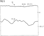
- FIG. 5 shows an enlarged schematic detail view of a preliminary semiconductor product for producing the semiconductor light emitting diode according to one of FIGS. 1 to 4 after sputtering on the oxide layer 8. Shown is an upper portion of the uppermost layer of the semiconductor layer stack 20 and the oxide layer of the transparent conductive oxide sputtered thereon.
- the uppermost semiconductor layer is either the p-doped semiconductor layer 5 of FIG. 1 or 3 or the n-doped semiconductor layer 7 FIG. 2 or 4.
- the roughness of the uppermost semiconductor layer predetermines the roughness R1 of the lower first interface 8a of the oxide layer 8; it is typically above 1.5 nm Rms, but may also be much larger - depending on the deposition process for the topmost semiconductor layer, its base material, and its dopant concentration.
- the roughness of their top is between 1.2 to 1.8 nm.
- the roughness R2 of its second interface 8b is as shown in FIG FIG. 5 shown smaller than the roughness R1 of the first interface 8a, in particular less than 1.0 nm or even 0.5 nm.
- the oxide layer 8 is sputtered in the embodiments described herein with a layer thickness of between 1 and 50 nm, wherein the layer thickness can also be selected to be larger. If the oxide layer is deposited with a minimum layer thickness of, for example, 5 nm, unevenness which results from the underlying semiconductor layer 5 or 7, respectively, is leveled during the sputtering of the oxide layer. This ensures that the roughness R2 of the second boundary surface 8b of the oxide layer 8 is influenced only by the HF-assisted DC sputtering method, but not by height fluctuations of lower-lying semiconductor layers.
- the mirror layers which are arranged on the (deposited by the HF-assisted DC sputtering) oxide layer, have extremely smooth reflection surfaces.
- the uppermost semiconductor layer of the semiconductor layer stack exposed before sputtering of the oxide layer 8 is hardly damaged by the RF-assisted DC sputtering method.
- the RF assisted DC sputtering process is used herein for depositing the oxide layer 8 from the transparent conductive oxide onto the uppermost layer of the Semiconductor layer stack 20 used for the light emitting diode.
- a high-frequency AC voltage is superimposed on a DC electrical voltage.
- the electrical power supplied for sputtering thus comprises a DC component (direct current) and a high-frequency component (HF; high frequency).
- the frequency of the high-frequency power component is, for example, 13.56 MHz.
- the combined DC / RF power is supplied, for example, to an electrode arranged in a sputtering chamber.
- the second interface 8b of the oxide layer 8 deposited by the RF-assisted DC sputtering method and the interfaces of the further mirror layers 18, 19 deposited on the second interface 8b reflect a higher proportion of the electromagnetic radiation impinging on them due to the reduced roughness. This applies in particular to those radiation components which impinge on these interfaces at relatively large angles of incidence relative to the surface normal.
- the semiconductor light-emitting diode 10 emits a greater intensity of electromagnetic radiation overall at its radiation exit surface 25.
Claims (13)
- Diode électroluminescente à semi-conducteur (10), ayant:- d'au moins une couche de diode électroluminescente dopée p (4), d'une couche de diode électroluminescente dopée n (2) ainsi que d'une zone active optique (3) entre la couche de diode électroluminescente dopée p (4) et la couche de diode électroluminescente dopée n (2),- d'une couche d'oxyde (8) en oxyde conducteur transparent, et- d'au moins une couche miroir (9),la couche d'oxyde (8) étant disposée entre les couches de diode électroluminescente (2, 4) et l'au moins une couche miroir (9), et présentant une première interface (8a) tournée vers les couches de diode électroluminescente (2, 4), et une deuxième interface (8b) tournée vers l'au moins une couche miroir (9), et
la couche miroir (9) étant adjacente à la deuxième interface (8b) de la couche d'oxyde (8),
caractérisée en ce que
la deuxième interface (8b) de la couche d'oxyde (8) possède une rugosité (R2) inférieure à 1,0 nm. - Diode électroluminescente à semi-conducteur selon la revendication 1,
caractérisée en ce que
la couche d'oxyde (8) possède une épaisseur de couche supérieure à 5 nm. - Diode électroluminescente à semi-conducteur selon la revendication 1 ou 2,
caractérisée en ce que
la couche de diode électroluminescente dopée p (4) est disposée plus proche de la couche d'oxyde (8) que ne l'est la couche de diode électroluminescente dopée n (2). - Diode électroluminescente à semi-conducteur selon l'une quelconque des revendications 1 à 3,
caractérisée en ce qu'
est disposée entre la couche de diode électroluminescente dopée p (4) et la couche d'oxyde (8) une couche de semi-conducteur dopé p (5) qui possède une concentration en dopant qui est au moins aussi élevée que la concentration en dopant de la couche de diode électroluminescente dopée p (4). - Diode électroluminescente à semi-conducteur selon la revendication 4,
caractérisée en ce que
la couche d'oxyde (8) est, par sa première interface (8a), adjacente à la couche de semi-conducteur dopé p (5). - Diode électroluminescente à semi-conducteur selon la revendication 4,
caractérisée en ce qu'
est disposée entre la couche de semi-conducteur dopé p (5) et la couche d'oxyde (8) une couche de semi-conducteur dopé n (7), et que la première interface (8a) de la couche d'oxyde (8) est adjacente à la couche de semi-conducteur dopé n. - Diode électroluminescente à semi-conducteur selon la revendication 6,
caractérisée en ce qu'
une couche de semi-conducteur non dopé (6) est disposée entre la couche de semi-conducteur dopé p (5) et la couche de semi-conducteur dopé n (7). - Diode électroluminescente à semi-conducteur selon l'une quelconque des revendications 1 à 7,
caractérisée en ce que
l'oxyde conducteur transparent de la couche d'oxyde (8) contient au moins une des matières oxyde de zinc, oxyde d'étain d'indium et oxyde de zinc d'indium. - Diode électroluminescente à semi-conducteur selon l'une quelconque des revendications 1 à 8,
caractérisée en ce que
la couche miroir (9) comprend au moins une couche miroir métallique (19). - Diode électroluminescente à semi-conducteur selon l'une quelconque des revendications 1 à 9,
caractérisée en ce que
la couche miroir (9) comprend au moins une couche miroir diélectrique (18). - Diode électroluminescente à semi-conducteur selon la revendication 10,
caractérisée en ce que
la couche miroir diélectrique (18) est disposée entre la couche d'oxyde (8) et la couche miroir métallique (19) et qu'elle présente des entailles locales (11) dans lesquelles la couche miroir métallique (19) va jusqu'à la deuxième interface (8b) de la couche d'oxyde (8). - Procédé de fabrication d'une diode électroluminescente à semi-conducteur (10), le procédé comprenant comme suit :- formation d'une couche de diode électroluminescente dopée p (4) et d'une couche de diode électroluminescente dopée n (2),- dépôt d'un oxyde conducteur transparent permettant de constituer une couche d'oxyde (8) qui présente une première interface (8a) tournée vers les couches de diode électroluminescente (2, 4), la couche d'oxyde (8) étant déposée par pulvérisation cathodique DC soutenue par pulvérisation RF et générant alors une deuxième interface (8b) de la couche d'oxyde (8) opposée à la première interface (8a), la deuxième interface (8b) de la couche d'oxyde (8) possédant une rugosité (R2) inférieure à 1,0 nm et une rugosité inférieure à celle de la première interface (8a) de la couche d'oxyde (8), et- formation d'au moins une couche miroir (9) au-dessus de la deuxième interface (8b) de la couche d'oxyde (8), la couche miroir (9) étant adjacente à la deuxième interface (8b) de la couche d'oxyde (8).
- Procédé selon la revendication 12,
caractérisé en ce que
la formation de l'au moins une couche miroir (9) comprend le dépôt d'au moins une couche miroir diélectrique (18), la gravure d'entailles dans la couche miroir diélectrique (18) et le dépôt d'au moins une couche miroir métallique (19) sur la couche miroir diélectrique (18).
Applications Claiming Priority (3)
| Application Number | Priority Date | Filing Date | Title |
|---|---|---|---|
| DE102008011847 | 2008-02-29 | ||
| DE102008027045A DE102008027045A1 (de) | 2008-02-29 | 2008-06-06 | Halbleiterleuchtdiode und Verfahren zur Herstellung einer Halbleiterleuchtdiode |
| PCT/DE2009/000192 WO2009106038A1 (fr) | 2008-02-29 | 2009-02-11 | Diode électroluminescente à semi-conducteur et procédé de fabrication d'une diode à semi-conducteur |
Publications (2)
| Publication Number | Publication Date |
|---|---|
| EP2248191A1 EP2248191A1 (fr) | 2010-11-10 |
| EP2248191B1 true EP2248191B1 (fr) | 2018-08-15 |
Family
ID=40911446
Family Applications (1)
| Application Number | Title | Priority Date | Filing Date |
|---|---|---|---|
| EP09714695.5A Active EP2248191B1 (fr) | 2008-02-29 | 2009-02-11 | Diode électroluminescente à semi-conducteur et procédé de fabrication d'une diode à semi-conducteur |
Country Status (8)
| Country | Link |
|---|---|
| US (1) | US8772804B2 (fr) |
| EP (1) | EP2248191B1 (fr) |
| JP (1) | JP2011513955A (fr) |
| KR (2) | KR101935642B1 (fr) |
| CN (1) | CN101960623B (fr) |
| DE (1) | DE102008027045A1 (fr) |
| TW (1) | TWI394297B (fr) |
| WO (1) | WO2009106038A1 (fr) |
Families Citing this family (10)
| Publication number | Priority date | Publication date | Assignee | Title |
|---|---|---|---|---|
| CN102194947B (zh) * | 2010-03-17 | 2015-11-25 | Lg伊诺特有限公司 | 发光器件和发光器件封装 |
| JP5830166B2 (ja) | 2011-05-25 | 2015-12-09 | オスラム オプト セミコンダクターズ ゲゼルシャフト ミット ベシュレンクテル ハフツングOsram Opto Semiconductors GmbH | オプトエレクトロニクス半導体チップ |
| TW201322489A (zh) * | 2011-11-29 | 2013-06-01 | Genesis Photonics Inc | 發光二極體元件及覆晶式發光二極體封裝元件 |
| CN103247732B (zh) * | 2012-02-14 | 2018-02-06 | 晶元光电股份有限公司 | 具有平整表面的电流扩散层的发光元件 |
| DE102012106998A1 (de) * | 2012-07-31 | 2014-02-06 | Osram Opto Semiconductors Gmbh | Reflektierendes Kontaktschichtsystem für ein optoelektronisches Bauelement und Verfahren zu dessen Herstellung |
| DE102015102454A1 (de) | 2015-02-20 | 2016-08-25 | Osram Opto Semiconductors Gmbh | Verfahren zur Strukturierung einer Nitridschicht, strukturierte Dielektrikumschicht, optoelektronisches Bauelement, Ätzverfahren zum Ätzen von Schichten und Umgebungssensor |
| DE102015108875B4 (de) * | 2015-06-04 | 2016-12-15 | Otto-Von-Guericke-Universität Magdeburg | Bauelement mit einer transparenten leitfähigen Nitridschicht |
| KR102519668B1 (ko) | 2016-06-21 | 2023-04-07 | 삼성전자주식회사 | 반도체 발광 소자 및 그 제조 방법 |
| KR102476139B1 (ko) | 2016-08-03 | 2022-12-09 | 삼성전자주식회사 | 반도체 발광소자 |
| KR102543183B1 (ko) | 2018-01-26 | 2023-06-14 | 삼성전자주식회사 | 반도체 발광소자 |
Citations (5)
| Publication number | Priority date | Publication date | Assignee | Title |
|---|---|---|---|---|
| US20030166308A1 (en) * | 1999-04-15 | 2003-09-04 | Sumitomo Electric Industries, Ltd. | Method of manufacturing transparent conductor film and compound semiconductor light -emitting device with the film |
| JP2004146541A (ja) * | 2002-10-23 | 2004-05-20 | Shin Etsu Handotai Co Ltd | 発光素子及び発光素子の製造方法 |
| US20040135166A1 (en) * | 2002-10-23 | 2004-07-15 | Shin-Etsu Handotai Co., Ltd. | Light-emitting device and method of fabricating the same |
| US20070020788A1 (en) * | 2005-07-12 | 2007-01-25 | Jin-Hsiang Liu | Fabrication method of high-brightness light emitting diode having reflective layer |
| WO2009083001A2 (fr) * | 2007-12-27 | 2009-07-09 | Osram Opto Semiconductors Gmbh | Corps émetteur de rayonnement et procédé pour produire un corps émetteur de rayonnement |
Family Cites Families (20)
| Publication number | Priority date | Publication date | Assignee | Title |
|---|---|---|---|---|
| JP2001009583A (ja) * | 1999-06-29 | 2001-01-16 | Canon Inc | レーザ加工装置 |
| DE10023459A1 (de) | 2000-05-12 | 2001-11-15 | Balzers Process Systems Gmbh | Indium-Zinn-Oxid (ITO)-Schicht und Verfahren zur Herstellung derselben |
| US6784462B2 (en) | 2001-12-13 | 2004-08-31 | Rensselaer Polytechnic Institute | Light-emitting diode with planar omni-directional reflector |
| EP1471583B1 (fr) | 2002-01-28 | 2009-10-07 | Nichia Corporation | Dispositif a semi-conducteur a base de nitrure comprenant un substrat de support, et son procede de realisation |
| KR20050051920A (ko) * | 2003-11-28 | 2005-06-02 | 삼성전자주식회사 | 플립칩형 질화물계 발광소자 및 그 제조방법 |
| US20050236630A1 (en) * | 2004-04-23 | 2005-10-27 | Wang-Nang Wang | Transparent contact for light emitting diode |
| DE102005013894B4 (de) | 2004-06-30 | 2010-06-17 | Osram Opto Semiconductors Gmbh | Elektromagnetische Strahlung erzeugender Halbleiterchip und Verfahren zu dessen Herstellung |
| DE102004050891B4 (de) | 2004-10-19 | 2019-01-10 | Lumileds Holding B.V. | Lichtmittierende III-Nitrid-Halbleitervorrichtung |
| KR101139891B1 (ko) | 2005-01-31 | 2012-04-27 | 렌슬러 폴리테크닉 인스티튜트 | 확산 반사면을 구비한 발광 다이오드 소자 |
| KR100609117B1 (ko) * | 2005-05-03 | 2006-08-08 | 삼성전기주식회사 | 질화물계 반도체 발광소자 및 그 제조방법 |
| DE102005035722B9 (de) | 2005-07-29 | 2021-11-18 | OSRAM Opto Semiconductors Gesellschaft mit beschränkter Haftung | Optoelektronischer Halbleiterchip und Verfahren zu dessen Herstellung |
| EP1750310A3 (fr) | 2005-08-03 | 2009-07-15 | Samsung Electro-Mechanics Co., Ltd. | Réflecteur omni-directionnel et diode électroluminescente pourvu de celui-ci |
| DE102006023685A1 (de) | 2005-09-29 | 2007-04-05 | Osram Opto Semiconductors Gmbh | Optoelektronischer Halbleiterchip |
| DE102005061346A1 (de) * | 2005-09-30 | 2007-04-05 | Osram Opto Semiconductors Gmbh | Optoelektronischer Halbleiterchip |
| CN101395728B (zh) | 2006-03-10 | 2011-04-13 | 松下电工株式会社 | 发光元件及其制造方法 |
| JP2007273975A (ja) * | 2006-03-10 | 2007-10-18 | Matsushita Electric Works Ltd | 発光素子 |
| DE102007002416A1 (de) * | 2006-04-13 | 2007-10-18 | Osram Opto Semiconductors Gmbh | Strahlungsemittierender Körper und Verfahren zur Herstellung eines strahlungsemittierenden Körpers |
| DE102007029370A1 (de) * | 2007-05-04 | 2008-11-06 | Osram Opto Semiconductors Gmbh | Halbleiterchip und Verfahren zur Herstellung eines Halbleiterchips |
| DE102007035687A1 (de) | 2007-07-30 | 2009-02-05 | Osram Opto Semiconductors Gmbh | Optoelektronisches Bauelement mit einem Schichtenstapel |
| US20090104733A1 (en) * | 2007-10-22 | 2009-04-23 | Yong Kee Chae | Microcrystalline silicon deposition for thin film solar applications |
-
2008
- 2008-06-06 DE DE102008027045A patent/DE102008027045A1/de not_active Withdrawn
-
2009
- 2009-02-11 US US12/920,311 patent/US8772804B2/en active Active
- 2009-02-11 KR KR1020167014288A patent/KR101935642B1/ko active IP Right Grant
- 2009-02-11 KR KR1020107019171A patent/KR101645738B1/ko active IP Right Grant
- 2009-02-11 CN CN200980107062.XA patent/CN101960623B/zh active Active
- 2009-02-11 JP JP2010547944A patent/JP2011513955A/ja active Pending
- 2009-02-11 WO PCT/DE2009/000192 patent/WO2009106038A1/fr active Application Filing
- 2009-02-11 EP EP09714695.5A patent/EP2248191B1/fr active Active
- 2009-02-25 TW TW98105936A patent/TWI394297B/zh not_active IP Right Cessation
Patent Citations (5)
| Publication number | Priority date | Publication date | Assignee | Title |
|---|---|---|---|---|
| US20030166308A1 (en) * | 1999-04-15 | 2003-09-04 | Sumitomo Electric Industries, Ltd. | Method of manufacturing transparent conductor film and compound semiconductor light -emitting device with the film |
| JP2004146541A (ja) * | 2002-10-23 | 2004-05-20 | Shin Etsu Handotai Co Ltd | 発光素子及び発光素子の製造方法 |
| US20040135166A1 (en) * | 2002-10-23 | 2004-07-15 | Shin-Etsu Handotai Co., Ltd. | Light-emitting device and method of fabricating the same |
| US20070020788A1 (en) * | 2005-07-12 | 2007-01-25 | Jin-Hsiang Liu | Fabrication method of high-brightness light emitting diode having reflective layer |
| WO2009083001A2 (fr) * | 2007-12-27 | 2009-07-09 | Osram Opto Semiconductors Gmbh | Corps émetteur de rayonnement et procédé pour produire un corps émetteur de rayonnement |
Also Published As
| Publication number | Publication date |
|---|---|
| US20110198640A1 (en) | 2011-08-18 |
| DE102008027045A1 (de) | 2009-09-03 |
| EP2248191A1 (fr) | 2010-11-10 |
| JP2011513955A (ja) | 2011-04-28 |
| TWI394297B (zh) | 2013-04-21 |
| KR101935642B1 (ko) | 2019-01-04 |
| CN101960623A (zh) | 2011-01-26 |
| US8772804B2 (en) | 2014-07-08 |
| KR20100126332A (ko) | 2010-12-01 |
| CN101960623B (zh) | 2014-08-06 |
| WO2009106038A1 (fr) | 2009-09-03 |
| TW200945635A (en) | 2009-11-01 |
| KR20160075765A (ko) | 2016-06-29 |
| KR101645738B1 (ko) | 2016-08-04 |
Similar Documents
| Publication | Publication Date | Title |
|---|---|---|
| EP2248191B1 (fr) | Diode électroluminescente à semi-conducteur et procédé de fabrication d'une diode à semi-conducteur | |
| EP3200247B1 (fr) | Puce semi-conductrice et procédé de fabrication d'une puce semi-conductrice | |
| EP2695207B1 (fr) | Puce semi-conductrice optoélectronique | |
| EP2193555B1 (fr) | Élément semi-conducteur optoélectronique | |
| DE102006034847A1 (de) | Optoelektronischer Halbleiterchip | |
| DE102006057747B4 (de) | Halbleiterkörper und Halbleiterchip mit einem Halbleiterkörper | |
| DE102004057802B4 (de) | Strahlungemittierendes Halbleiterbauelement mit Zwischenschicht | |
| EP2057696B1 (fr) | Puce de semiconducteur optoélectronique et procédé de sa fabrication | |
| DE112017000332B4 (de) | Optoelektronisches Bauelement und Verfahren zur Herstellung eines optoelektronischen Bauelements | |
| EP2270875A1 (fr) | Dispositf à semiconducteur émetteur de lumière et son procédé de fabrication | |
| DE102012101718A1 (de) | Optoelektronischer Halbleiterchip | |
| DE112017003307T5 (de) | Verfahren zur Herstellung einer optischen Halbleitervorrichtung und optische Halbleitervorrichtung | |
| EP1770792B1 (fr) | Puce à semi-conducteur émetteur de lumière | |
| WO2012107289A1 (fr) | Puce semiconductrice optoélectronique à couche miroir encapsulée | |
| EP1665398B1 (fr) | Puce semi-conductrice en couche mince emettant un rayonnement | |
| EP2338182B1 (fr) | Composant optoélectronique à semi-conducteur | |
| DE112019002037B4 (de) | Lichtemittierende Halbleiterelemente und Verfahren zu deren Herstellung | |
| EP2313935A1 (fr) | Puce semiconductrice optoélectronique | |
| WO2018233950A1 (fr) | Puce semi-conductrice comprenant des paliers intérieurs similaires à des terrasses et procédé de fabrication d'une puce semi-conductrice | |
| DE19838430C2 (de) | Verfahren zur Herstellung eines Arrays von Photodetektoren | |
| WO2009015645A2 (fr) | Composant optoélectronique avec un empilement de couches | |
| WO2020165029A1 (fr) | Composant à semi-conducteur optoélectronique comprenant des parties d'une couche conductrice et procédé de fabrication du composant à semi-conducteur optoélectronique | |
| DE102018107470A1 (de) | Optoelektronischer halbleiterchip und verfahren zur herstellung eines optoelektronischen halbleiterchips | |
| DE102017105397A1 (de) | Verfahren zur Herstellung von Leuchtdioden und Leuchtdiode | |
| DE102016101612A1 (de) | Optoelektronischer Halbleiterchip und Verfahren zur Herstellung eines optoelektronischen Halbleiterchips |
Legal Events
| Date | Code | Title | Description |
|---|---|---|---|
| PUAI | Public reference made under article 153(3) epc to a published international application that has entered the european phase |
Free format text: ORIGINAL CODE: 0009012 |
|
| 17P | Request for examination filed |
Effective date: 20100805 |
|
| AK | Designated contracting states |
Kind code of ref document: A1 Designated state(s): AT BE BG CH CY CZ DE DK EE ES FI FR GB GR HR HU IE IS IT LI LT LU LV MC MK MT NL NO PL PT RO SE SI SK TR |
|
| AX | Request for extension of the european patent |
Extension state: AL BA RS |
|
| DAX | Request for extension of the european patent (deleted) | ||
| STAA | Information on the status of an ep patent application or granted ep patent |
Free format text: STATUS: EXAMINATION IS IN PROGRESS |
|
| 17Q | First examination report despatched |
Effective date: 20170517 |
|
| REG | Reference to a national code |
Ref country code: DE Ref legal event code: R079 Ref document number: 502009015195 Country of ref document: DE Free format text: PREVIOUS MAIN CLASS: H01L0033000000 Ipc: H01L0033400000 |
|
| RIC1 | Information provided on ipc code assigned before grant |
Ipc: H01L 33/40 20100101AFI20180322BHEP Ipc: H01L 33/42 20100101ALI20180322BHEP |
|
| GRAP | Despatch of communication of intention to grant a patent |
Free format text: ORIGINAL CODE: EPIDOSNIGR1 |
|
| STAA | Information on the status of an ep patent application or granted ep patent |
Free format text: STATUS: GRANT OF PATENT IS INTENDED |
|
| INTG | Intention to grant announced |
Effective date: 20180508 |
|
| GRAS | Grant fee paid |
Free format text: ORIGINAL CODE: EPIDOSNIGR3 |
|
| GRAA | (expected) grant |
Free format text: ORIGINAL CODE: 0009210 |
|
| STAA | Information on the status of an ep patent application or granted ep patent |
Free format text: STATUS: THE PATENT HAS BEEN GRANTED |
|
| AK | Designated contracting states |
Kind code of ref document: B1 Designated state(s): AT BE BG CH CY CZ DE DK EE ES FI FR GB GR HR HU IE IS IT LI LT LU LV MC MK MT NL NO PL PT RO SE SI SK TR |
|
| REG | Reference to a national code |
Ref country code: CH Ref legal event code: EP Ref country code: GB Ref legal event code: FG4D Free format text: NOT ENGLISH Ref country code: AT Ref legal event code: REF Ref document number: 1030769 Country of ref document: AT Kind code of ref document: T Effective date: 20180815 |
|
| REG | Reference to a national code |
Ref country code: IE Ref legal event code: FG4D Free format text: LANGUAGE OF EP DOCUMENT: GERMAN |
|
| REG | Reference to a national code |
Ref country code: DE Ref legal event code: R096 Ref document number: 502009015195 Country of ref document: DE |
|
| REG | Reference to a national code |
Ref country code: NL Ref legal event code: MP Effective date: 20180815 |
|
| REG | Reference to a national code |
Ref country code: LT Ref legal event code: MG4D |
|
| PG25 | Lapsed in a contracting state [announced via postgrant information from national office to epo] |
Ref country code: BG Free format text: LAPSE BECAUSE OF FAILURE TO SUBMIT A TRANSLATION OF THE DESCRIPTION OR TO PAY THE FEE WITHIN THE PRESCRIBED TIME-LIMIT Effective date: 20181115 Ref country code: SE Free format text: LAPSE BECAUSE OF FAILURE TO SUBMIT A TRANSLATION OF THE DESCRIPTION OR TO PAY THE FEE WITHIN THE PRESCRIBED TIME-LIMIT Effective date: 20180815 Ref country code: NL Free format text: LAPSE BECAUSE OF FAILURE TO SUBMIT A TRANSLATION OF THE DESCRIPTION OR TO PAY THE FEE WITHIN THE PRESCRIBED TIME-LIMIT Effective date: 20180815 Ref country code: NO Free format text: LAPSE BECAUSE OF FAILURE TO SUBMIT A TRANSLATION OF THE DESCRIPTION OR TO PAY THE FEE WITHIN THE PRESCRIBED TIME-LIMIT Effective date: 20181115 Ref country code: IS Free format text: LAPSE BECAUSE OF FAILURE TO SUBMIT A TRANSLATION OF THE DESCRIPTION OR TO PAY THE FEE WITHIN THE PRESCRIBED TIME-LIMIT Effective date: 20181215 Ref country code: LT Free format text: LAPSE BECAUSE OF FAILURE TO SUBMIT A TRANSLATION OF THE DESCRIPTION OR TO PAY THE FEE WITHIN THE PRESCRIBED TIME-LIMIT Effective date: 20180815 Ref country code: FI Free format text: LAPSE BECAUSE OF FAILURE TO SUBMIT A TRANSLATION OF THE DESCRIPTION OR TO PAY THE FEE WITHIN THE PRESCRIBED TIME-LIMIT Effective date: 20180815 Ref country code: GR Free format text: LAPSE BECAUSE OF FAILURE TO SUBMIT A TRANSLATION OF THE DESCRIPTION OR TO PAY THE FEE WITHIN THE PRESCRIBED TIME-LIMIT Effective date: 20181116 |
|
| PG25 | Lapsed in a contracting state [announced via postgrant information from national office to epo] |
Ref country code: ES Free format text: LAPSE BECAUSE OF FAILURE TO SUBMIT A TRANSLATION OF THE DESCRIPTION OR TO PAY THE FEE WITHIN THE PRESCRIBED TIME-LIMIT Effective date: 20180815 Ref country code: HR Free format text: LAPSE BECAUSE OF FAILURE TO SUBMIT A TRANSLATION OF THE DESCRIPTION OR TO PAY THE FEE WITHIN THE PRESCRIBED TIME-LIMIT Effective date: 20180815 Ref country code: LV Free format text: LAPSE BECAUSE OF FAILURE TO SUBMIT A TRANSLATION OF THE DESCRIPTION OR TO PAY THE FEE WITHIN THE PRESCRIBED TIME-LIMIT Effective date: 20180815 |
|
| PG25 | Lapsed in a contracting state [announced via postgrant information from national office to epo] |
Ref country code: RO Free format text: LAPSE BECAUSE OF FAILURE TO SUBMIT A TRANSLATION OF THE DESCRIPTION OR TO PAY THE FEE WITHIN THE PRESCRIBED TIME-LIMIT Effective date: 20180815 Ref country code: EE Free format text: LAPSE BECAUSE OF FAILURE TO SUBMIT A TRANSLATION OF THE DESCRIPTION OR TO PAY THE FEE WITHIN THE PRESCRIBED TIME-LIMIT Effective date: 20180815 Ref country code: IT Free format text: LAPSE BECAUSE OF FAILURE TO SUBMIT A TRANSLATION OF THE DESCRIPTION OR TO PAY THE FEE WITHIN THE PRESCRIBED TIME-LIMIT Effective date: 20180815 Ref country code: PL Free format text: LAPSE BECAUSE OF FAILURE TO SUBMIT A TRANSLATION OF THE DESCRIPTION OR TO PAY THE FEE WITHIN THE PRESCRIBED TIME-LIMIT Effective date: 20180815 Ref country code: CZ Free format text: LAPSE BECAUSE OF FAILURE TO SUBMIT A TRANSLATION OF THE DESCRIPTION OR TO PAY THE FEE WITHIN THE PRESCRIBED TIME-LIMIT Effective date: 20180815 |
|
| REG | Reference to a national code |
Ref country code: DE Ref legal event code: R097 Ref document number: 502009015195 Country of ref document: DE |
|
| PG25 | Lapsed in a contracting state [announced via postgrant information from national office to epo] |
Ref country code: SK Free format text: LAPSE BECAUSE OF FAILURE TO SUBMIT A TRANSLATION OF THE DESCRIPTION OR TO PAY THE FEE WITHIN THE PRESCRIBED TIME-LIMIT Effective date: 20180815 Ref country code: DK Free format text: LAPSE BECAUSE OF FAILURE TO SUBMIT A TRANSLATION OF THE DESCRIPTION OR TO PAY THE FEE WITHIN THE PRESCRIBED TIME-LIMIT Effective date: 20180815 |
|
| PLBE | No opposition filed within time limit |
Free format text: ORIGINAL CODE: 0009261 |
|
| STAA | Information on the status of an ep patent application or granted ep patent |
Free format text: STATUS: NO OPPOSITION FILED WITHIN TIME LIMIT |
|
| 26N | No opposition filed |
Effective date: 20190516 |
|
| PG25 | Lapsed in a contracting state [announced via postgrant information from national office to epo] |
Ref country code: SI Free format text: LAPSE BECAUSE OF FAILURE TO SUBMIT A TRANSLATION OF THE DESCRIPTION OR TO PAY THE FEE WITHIN THE PRESCRIBED TIME-LIMIT Effective date: 20180815 |
|
| REG | Reference to a national code |
Ref country code: CH Ref legal event code: PL |
|
| GBPC | Gb: european patent ceased through non-payment of renewal fee |
Effective date: 20190211 |
|
| PG25 | Lapsed in a contracting state [announced via postgrant information from national office to epo] |
Ref country code: LU Free format text: LAPSE BECAUSE OF NON-PAYMENT OF DUE FEES Effective date: 20190211 Ref country code: MC Free format text: LAPSE BECAUSE OF FAILURE TO SUBMIT A TRANSLATION OF THE DESCRIPTION OR TO PAY THE FEE WITHIN THE PRESCRIBED TIME-LIMIT Effective date: 20180815 |
|
| REG | Reference to a national code |
Ref country code: BE Ref legal event code: MM Effective date: 20190228 |
|
| REG | Reference to a national code |
Ref country code: IE Ref legal event code: MM4A |
|
| PG25 | Lapsed in a contracting state [announced via postgrant information from national office to epo] |
Ref country code: CH Free format text: LAPSE BECAUSE OF NON-PAYMENT OF DUE FEES Effective date: 20190228 Ref country code: LI Free format text: LAPSE BECAUSE OF NON-PAYMENT OF DUE FEES Effective date: 20190228 |
|
| PG25 | Lapsed in a contracting state [announced via postgrant information from national office to epo] |
Ref country code: IE Free format text: LAPSE BECAUSE OF NON-PAYMENT OF DUE FEES Effective date: 20190211 Ref country code: GB Free format text: LAPSE BECAUSE OF NON-PAYMENT OF DUE FEES Effective date: 20190211 |
|
| PG25 | Lapsed in a contracting state [announced via postgrant information from national office to epo] |
Ref country code: FR Free format text: LAPSE BECAUSE OF NON-PAYMENT OF DUE FEES Effective date: 20190228 Ref country code: BE Free format text: LAPSE BECAUSE OF NON-PAYMENT OF DUE FEES Effective date: 20190228 |
|
| PG25 | Lapsed in a contracting state [announced via postgrant information from national office to epo] |
Ref country code: TR Free format text: LAPSE BECAUSE OF FAILURE TO SUBMIT A TRANSLATION OF THE DESCRIPTION OR TO PAY THE FEE WITHIN THE PRESCRIBED TIME-LIMIT Effective date: 20180815 |
|
| REG | Reference to a national code |
Ref country code: AT Ref legal event code: MM01 Ref document number: 1030769 Country of ref document: AT Kind code of ref document: T Effective date: 20190211 |
|
| PG25 | Lapsed in a contracting state [announced via postgrant information from national office to epo] |
Ref country code: AT Free format text: LAPSE BECAUSE OF NON-PAYMENT OF DUE FEES Effective date: 20190211 |
|
| PG25 | Lapsed in a contracting state [announced via postgrant information from national office to epo] |
Ref country code: MT Free format text: LAPSE BECAUSE OF FAILURE TO SUBMIT A TRANSLATION OF THE DESCRIPTION OR TO PAY THE FEE WITHIN THE PRESCRIBED TIME-LIMIT Effective date: 20180815 Ref country code: PT Free format text: LAPSE BECAUSE OF FAILURE TO SUBMIT A TRANSLATION OF THE DESCRIPTION OR TO PAY THE FEE WITHIN THE PRESCRIBED TIME-LIMIT Effective date: 20181215 |
|
| PG25 | Lapsed in a contracting state [announced via postgrant information from national office to epo] |
Ref country code: CY Free format text: LAPSE BECAUSE OF FAILURE TO SUBMIT A TRANSLATION OF THE DESCRIPTION OR TO PAY THE FEE WITHIN THE PRESCRIBED TIME-LIMIT Effective date: 20180815 |
|
| PG25 | Lapsed in a contracting state [announced via postgrant information from national office to epo] |
Ref country code: HU Free format text: LAPSE BECAUSE OF FAILURE TO SUBMIT A TRANSLATION OF THE DESCRIPTION OR TO PAY THE FEE WITHIN THE PRESCRIBED TIME-LIMIT; INVALID AB INITIO Effective date: 20090211 |
|
| PG25 | Lapsed in a contracting state [announced via postgrant information from national office to epo] |
Ref country code: MK Free format text: LAPSE BECAUSE OF FAILURE TO SUBMIT A TRANSLATION OF THE DESCRIPTION OR TO PAY THE FEE WITHIN THE PRESCRIBED TIME-LIMIT Effective date: 20180815 |
|
| P01 | Opt-out of the competence of the unified patent court (upc) registered |
Effective date: 20230825 |
|
| PGFP | Annual fee paid to national office [announced via postgrant information from national office to epo] |
Ref country code: DE Payment date: 20240219 Year of fee payment: 16 |