JP2011513955A - 半導体発光ダイオードおよび半導体発光ダイオードの製造方法 - Google Patents
半導体発光ダイオードおよび半導体発光ダイオードの製造方法 Download PDFInfo
- Publication number
- JP2011513955A JP2011513955A JP2010547944A JP2010547944A JP2011513955A JP 2011513955 A JP2011513955 A JP 2011513955A JP 2010547944 A JP2010547944 A JP 2010547944A JP 2010547944 A JP2010547944 A JP 2010547944A JP 2011513955 A JP2011513955 A JP 2011513955A
- Authority
- JP
- Japan
- Prior art keywords
- layer
- emitting diode
- light emitting
- type doped
- oxide
- Prior art date
- Legal status (The legal status is an assumption and is not a legal conclusion. Google has not performed a legal analysis and makes no representation as to the accuracy of the status listed.)
- Pending
Links
Images


Classifications
-
- H—ELECTRICITY
- H01—ELECTRIC ELEMENTS
- H01L—SEMICONDUCTOR DEVICES NOT COVERED BY CLASS H10
- H01L33/00—Semiconductor devices with at least one potential-jump barrier or surface barrier specially adapted for light emission; Processes or apparatus specially adapted for the manufacture or treatment thereof or of parts thereof; Details thereof
- H01L33/02—Semiconductor devices with at least one potential-jump barrier or surface barrier specially adapted for light emission; Processes or apparatus specially adapted for the manufacture or treatment thereof or of parts thereof; Details thereof characterised by the semiconductor bodies
- H01L33/20—Semiconductor devices with at least one potential-jump barrier or surface barrier specially adapted for light emission; Processes or apparatus specially adapted for the manufacture or treatment thereof or of parts thereof; Details thereof characterised by the semiconductor bodies with a particular shape, e.g. curved or truncated substrate
- H01L33/22—Roughened surfaces, e.g. at the interface between epitaxial layers
-
- H—ELECTRICITY
- H01—ELECTRIC ELEMENTS
- H01L—SEMICONDUCTOR DEVICES NOT COVERED BY CLASS H10
- H01L33/00—Semiconductor devices with at least one potential-jump barrier or surface barrier specially adapted for light emission; Processes or apparatus specially adapted for the manufacture or treatment thereof or of parts thereof; Details thereof
- H01L33/36—Semiconductor devices with at least one potential-jump barrier or surface barrier specially adapted for light emission; Processes or apparatus specially adapted for the manufacture or treatment thereof or of parts thereof; Details thereof characterised by the electrodes
- H01L33/40—Materials therefor
- H01L33/405—Reflective materials
-
- H—ELECTRICITY
- H01—ELECTRIC ELEMENTS
- H01L—SEMICONDUCTOR DEVICES NOT COVERED BY CLASS H10
- H01L33/00—Semiconductor devices with at least one potential-jump barrier or surface barrier specially adapted for light emission; Processes or apparatus specially adapted for the manufacture or treatment thereof or of parts thereof; Details thereof
- H01L33/02—Semiconductor devices with at least one potential-jump barrier or surface barrier specially adapted for light emission; Processes or apparatus specially adapted for the manufacture or treatment thereof or of parts thereof; Details thereof characterised by the semiconductor bodies
- H01L33/10—Semiconductor devices with at least one potential-jump barrier or surface barrier specially adapted for light emission; Processes or apparatus specially adapted for the manufacture or treatment thereof or of parts thereof; Details thereof characterised by the semiconductor bodies with a light reflecting structure, e.g. semiconductor Bragg reflector
-
- H—ELECTRICITY
- H01—ELECTRIC ELEMENTS
- H01L—SEMICONDUCTOR DEVICES NOT COVERED BY CLASS H10
- H01L33/00—Semiconductor devices with at least one potential-jump barrier or surface barrier specially adapted for light emission; Processes or apparatus specially adapted for the manufacture or treatment thereof or of parts thereof; Details thereof
- H01L33/36—Semiconductor devices with at least one potential-jump barrier or surface barrier specially adapted for light emission; Processes or apparatus specially adapted for the manufacture or treatment thereof or of parts thereof; Details thereof characterised by the electrodes
- H01L33/40—Materials therefor
- H01L33/42—Transparent materials
-
- H—ELECTRICITY
- H01—ELECTRIC ELEMENTS
- H01L—SEMICONDUCTOR DEVICES NOT COVERED BY CLASS H10
- H01L33/00—Semiconductor devices with at least one potential-jump barrier or surface barrier specially adapted for light emission; Processes or apparatus specially adapted for the manufacture or treatment thereof or of parts thereof; Details thereof
- H01L33/44—Semiconductor devices with at least one potential-jump barrier or surface barrier specially adapted for light emission; Processes or apparatus specially adapted for the manufacture or treatment thereof or of parts thereof; Details thereof characterised by the coatings, e.g. passivation layer or anti-reflective coating
- H01L33/46—Reflective coating, e.g. dielectric Bragg reflector
Landscapes
- Engineering & Computer Science (AREA)
- Manufacturing & Machinery (AREA)
- Computer Hardware Design (AREA)
- Microelectronics & Electronic Packaging (AREA)
- Power Engineering (AREA)
- Led Devices (AREA)
Abstract
Description
− 少なくとも1層のp型ドープ発光ダイオード層とn型ドープ発光ダイオード層とを形成するステップ、
− 透明導電性酸化物を堆積させるステップであって、これによって、発光ダイオード層に面している第1の境界面を備えている酸化物層が形成され、酸化物層が、高周波(HF)を利用する直流(DC)スパッタリング(HF-assisted DC sputtering)によって堆積され、この堆積において、第1の境界面に向かい合う、酸化物層の第2の境界面が形成され、この第2の境界面が、酸化物層の第1の境界面よりも小さい粗さを有する、ステップ、
− 酸化物層の第2の境界面の上に少なくとも1層のミラー層を形成するステップ、
を含んでいる。
Claims (15)
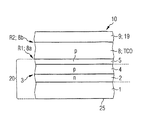
- 半導体発光ダイオード(10)であって、
− 少なくとも1層のp型ドープ発光ダイオード層(4)と、n型ドープ発光ダイオード層(2)と、前記p型ドープ発光ダイオード層(4)と前記n型ドープ発光ダイオード層(2)との間の光学活性ゾーン(3)と、
− 透明導電性酸化物の酸化物層(8)と、
− 少なくとも1層のミラー層(9)と、
を有し、
前記酸化物層(8)が、前記発光ダイオード層(2,4)と前記少なくとも1層のミラー層(9)との間に配置されており、前記酸化物層(8)が、前記発光ダイオード層(2,4)に面している第1の境界面(8a)と、前記少なくとも1層のミラー層(9)に面している第2の境界面(8b)と、を備えており、
前記酸化物層(8)の前記第2の境界面(8b)が、前記酸化物層(8)の前記第1の境界面(8a)よりも小さい粗さ(R2)を有する、
半導体発光ダイオード。 - 半導体発光ダイオード(10)であって、
− 少なくとも1層のp型ドープ発光ダイオード層(4)と、n型ドープ発光ダイオード層(2)と、前記p型ドープ発光ダイオード層(4)と前記n型ドープ発光ダイオード層(2)との間の光学活性ゾーン(3)と、
− 透明導電性酸化物の酸化物層(8)と、
− 少なくとも1層のミラー層(9)と、
前記酸化物層(8)が、前記発光ダイオード層(2,4)と前記少なくとも1層のミラー層(9)との間に配置されており、前記酸化物層(8)が、前記発光ダイオード層(2,4)に面している第1の境界面(8a)と、前記少なくとも1層のミラー層(9)に面している第2の境界面(8b)と、を備えており、
前記酸化物層(8)の前記第2の境界面(8b)が、1.0nm未満の粗さ(R2)を有する、
半導体発光ダイオード。 - 前記酸化物層(8)が、5nmより大きい層厚さを有することを特徴とする、
請求項1または2に記載の半導体発光ダイオード。 - 前記p型ドープ発光ダイオード層(4)が、前記n型ドープ発光ダイオード層(2)よりも前記酸化物層(8)の近傍に配置されていることを特徴とする、
請求項1〜3のいずれか1項に記載の半導体発光ダイオード。 - 前記p型ドープ発光ダイオード層(4)と前記酸化物層(8)との間に、p型ドープ半導体層(5)が配置されており、前記p型ドープ半導体層(5)が、前記p型ドープ発光ダイオード層(4)のドーパント濃度と同じかまたはそれより高いドーパント濃度を有することを特徴とする、
請求項1〜4のいずれか1項に記載の半導体発光ダイオード。 - 前記酸化物層(8)が、その前記第1の境界面(8a)において、前記p型ドープ半導体層(5)に隣接していることを特徴とする、
請求項5に記載の半導体発光ダイオード。 - 前記p型ドープ半導体層(5)と前記酸化物層(8)との間にn型ドープ半導体層(7)が配置されており、前記酸化物層(8)の前記第1の境界面(8a)が、前記n型ドープ半導体層(7)に隣接していることを特徴とする、
請求項5に記載の半導体発光ダイオード。 - 前記p型ドープ半導体層(5)と前記n型ドープ半導体層(7)との間にアンドープ半導体層(6)が配置されていることを特徴とする、
請求項7に記載の半導体発光ダイオード。 - 前記酸化物層(8)の前記透明導電性酸化物が、材料として酸化亜鉛、インジウムスズ酸化物、インジウム亜鉛酸化物のうちの少なくとも1つを含んでいることを特徴とする、
請求項1〜8のいずれか1項に記載の半導体発光ダイオード。 - 前記ミラー層(9)が前記酸化物層(8)の前記第2の境界面(8b)に隣接していることを特徴とする、
請求項1〜9のいずれか1項に記載の半導体発光ダイオード。 - 前記ミラー層(9)が、少なくとも1層の金属ミラー層(19)を備えていることを特徴とする、
請求項1〜10のいずれか1項に記載の半導体発光ダイオード。 - 前記ミラー層(9)が、少なくとも1層の誘電体ミラー層(18)を備えていることを特徴とする、
請求項1〜11のいずれか1項に記載の半導体発光ダイオード。 - 前記誘電体ミラー層(18)が、前記酸化物層(8)と前記金属ミラー層(19)との間に配置されており、前記誘電体ミラー層(18)が局所的な凹部(11)を備えており、前記凹部(11)の中で前記金属ミラー層(19)が前記酸化物層(8)の前記第2の境界面(8b)まで延在していることを特徴とする、
請求項12に記載の半導体発光ダイオード。 - 半導体発光ダイオード(10)を製造する方法であって、
− 少なくとも1層のp型ドープ発光ダイオード層(4)とn型ドープ発光ダイオード層(2)とを形成するステップと、
− 透明導電性酸化物を堆積させるステップであって、これによって、前記発光ダイオード層(2,4)に面している第1の境界面(8a)を備えている酸化物層(8)が形成され、前記酸化物層(8)が、HF支援DCスパッタリングによって堆積され、この堆積において、前記第1の境界面(8a)に向かい合う、前記酸化物層(8)の第2の境界面(8b)が形成され、前記第2の境界面(8b)が、前記酸化物層(8)の前記第1の境界面(8a)よりも小さい粗さを有する、前記ステップと、
− 前記酸化物層(8)の前記第2の境界面(8b)の上に少なくとも1層のミラー層(9)を形成するステップと、
を含んでいる、方法。 - 前記少なくとも1層のミラー層(9)を形成する前記ステップが、
少なくとも1層の誘電体ミラー層(18)を堆積させるステップと、前記誘電体ミラー層(18)に凹部をエッチングするステップと、前記誘電体ミラー層(18)の上に少なくとも1層の金属ミラー層(19)を堆積させるステップと、
を含んでいることを特徴とする、
請求項14に記載の方法。
Applications Claiming Priority (3)
| Application Number | Priority Date | Filing Date | Title |
|---|---|---|---|
| DE102008011847 | 2008-02-29 | ||
| DE102008027045A DE102008027045A1 (de) | 2008-02-29 | 2008-06-06 | Halbleiterleuchtdiode und Verfahren zur Herstellung einer Halbleiterleuchtdiode |
| PCT/DE2009/000192 WO2009106038A1 (de) | 2008-02-29 | 2009-02-11 | Halbleiterleuchtdiode und verfahren zur herstellung einer halbleiterleuchtdiode |
Publications (2)
| Publication Number | Publication Date |
|---|---|
| JP2011513955A true JP2011513955A (ja) | 2011-04-28 |
| JP2011513955A5 JP2011513955A5 (ja) | 2012-03-22 |
Family
ID=40911446
Family Applications (1)
| Application Number | Title | Priority Date | Filing Date |
|---|---|---|---|
| JP2010547944A Pending JP2011513955A (ja) | 2008-02-29 | 2009-02-11 | 半導体発光ダイオードおよび半導体発光ダイオードの製造方法 |
Country Status (8)
| Country | Link |
|---|---|
| US (1) | US8772804B2 (ja) |
| EP (1) | EP2248191B1 (ja) |
| JP (1) | JP2011513955A (ja) |
| KR (2) | KR101935642B1 (ja) |
| CN (1) | CN101960623B (ja) |
| DE (1) | DE102008027045A1 (ja) |
| TW (1) | TWI394297B (ja) |
| WO (1) | WO2009106038A1 (ja) |
Families Citing this family (10)
| Publication number | Priority date | Publication date | Assignee | Title |
|---|---|---|---|---|
| CN102194947B (zh) * | 2010-03-17 | 2015-11-25 | Lg伊诺特有限公司 | 发光器件和发光器件封装 |
| JP5830166B2 (ja) | 2011-05-25 | 2015-12-09 | オスラム オプト セミコンダクターズ ゲゼルシャフト ミット ベシュレンクテル ハフツングOsram Opto Semiconductors GmbH | オプトエレクトロニクス半導体チップ |
| TW201322489A (zh) * | 2011-11-29 | 2013-06-01 | Genesis Photonics Inc | 發光二極體元件及覆晶式發光二極體封裝元件 |
| CN103247732B (zh) * | 2012-02-14 | 2018-02-06 | 晶元光电股份有限公司 | 具有平整表面的电流扩散层的发光元件 |
| DE102012106998A1 (de) * | 2012-07-31 | 2014-02-06 | Osram Opto Semiconductors Gmbh | Reflektierendes Kontaktschichtsystem für ein optoelektronisches Bauelement und Verfahren zu dessen Herstellung |
| DE102015102454A1 (de) | 2015-02-20 | 2016-08-25 | Osram Opto Semiconductors Gmbh | Verfahren zur Strukturierung einer Nitridschicht, strukturierte Dielektrikumschicht, optoelektronisches Bauelement, Ätzverfahren zum Ätzen von Schichten und Umgebungssensor |
| DE102015108875B4 (de) * | 2015-06-04 | 2016-12-15 | Otto-Von-Guericke-Universität Magdeburg | Bauelement mit einer transparenten leitfähigen Nitridschicht |
| KR102519668B1 (ko) | 2016-06-21 | 2023-04-07 | 삼성전자주식회사 | 반도체 발광 소자 및 그 제조 방법 |
| KR102476139B1 (ko) | 2016-08-03 | 2022-12-09 | 삼성전자주식회사 | 반도체 발광소자 |
| KR102543183B1 (ko) | 2018-01-26 | 2023-06-14 | 삼성전자주식회사 | 반도체 발광소자 |
Citations (3)
| Publication number | Priority date | Publication date | Assignee | Title |
|---|---|---|---|---|
| JP2003532997A (ja) * | 2000-05-12 | 2003-11-05 | ウンアクシス ドイチェランド ゲーエムベーハー | インジウム−スズ酸化物(ito)フィルム及びその製造方法 |
| JP2006313888A (ja) * | 2005-05-03 | 2006-11-16 | Samsung Electro Mech Co Ltd | 窒化物系半導体発光素子及びその製造方法 |
| JP2007273975A (ja) * | 2006-03-10 | 2007-10-18 | Matsushita Electric Works Ltd | 発光素子 |
Family Cites Families (22)
| Publication number | Priority date | Publication date | Assignee | Title |
|---|---|---|---|---|
| US6876003B1 (en) * | 1999-04-15 | 2005-04-05 | Sumitomo Electric Industries, Ltd. | Semiconductor light-emitting device, method of manufacturing transparent conductor film and method of manufacturing compound semiconductor light-emitting device |
| JP2001009583A (ja) * | 1999-06-29 | 2001-01-16 | Canon Inc | レーザ加工装置 |
| US6784462B2 (en) | 2001-12-13 | 2004-08-31 | Rensselaer Polytechnic Institute | Light-emitting diode with planar omni-directional reflector |
| EP1471583B1 (en) | 2002-01-28 | 2009-10-07 | Nichia Corporation | Nitride semiconductor device having support substrate and its manufacturing method |
| US7041529B2 (en) * | 2002-10-23 | 2006-05-09 | Shin-Etsu Handotai Co., Ltd. | Light-emitting device and method of fabricating the same |
| JP4174581B2 (ja) * | 2002-10-23 | 2008-11-05 | 信越半導体株式会社 | 発光素子の製造方法 |
| KR20050051920A (ko) * | 2003-11-28 | 2005-06-02 | 삼성전자주식회사 | 플립칩형 질화물계 발광소자 및 그 제조방법 |
| US20050236630A1 (en) * | 2004-04-23 | 2005-10-27 | Wang-Nang Wang | Transparent contact for light emitting diode |
| DE102005013894B4 (de) | 2004-06-30 | 2010-06-17 | Osram Opto Semiconductors Gmbh | Elektromagnetische Strahlung erzeugender Halbleiterchip und Verfahren zu dessen Herstellung |
| DE102004050891B4 (de) | 2004-10-19 | 2019-01-10 | Lumileds Holding B.V. | Lichtmittierende III-Nitrid-Halbleitervorrichtung |
| KR101139891B1 (ko) | 2005-01-31 | 2012-04-27 | 렌슬러 폴리테크닉 인스티튜트 | 확산 반사면을 구비한 발광 다이오드 소자 |
| US7384808B2 (en) | 2005-07-12 | 2008-06-10 | Visual Photonics Epitaxy Co., Ltd. | Fabrication method of high-brightness light emitting diode having reflective layer |
| DE102005035722B9 (de) | 2005-07-29 | 2021-11-18 | OSRAM Opto Semiconductors Gesellschaft mit beschränkter Haftung | Optoelektronischer Halbleiterchip und Verfahren zu dessen Herstellung |
| EP1750310A3 (en) | 2005-08-03 | 2009-07-15 | Samsung Electro-Mechanics Co., Ltd. | Omni-directional reflector and light emitting diode adopting the same |
| DE102006023685A1 (de) | 2005-09-29 | 2007-04-05 | Osram Opto Semiconductors Gmbh | Optoelektronischer Halbleiterchip |
| DE102005061346A1 (de) * | 2005-09-30 | 2007-04-05 | Osram Opto Semiconductors Gmbh | Optoelektronischer Halbleiterchip |
| CN101395728B (zh) | 2006-03-10 | 2011-04-13 | 松下电工株式会社 | 发光元件及其制造方法 |
| DE102007002416A1 (de) * | 2006-04-13 | 2007-10-18 | Osram Opto Semiconductors Gmbh | Strahlungsemittierender Körper und Verfahren zur Herstellung eines strahlungsemittierenden Körpers |
| DE102007029370A1 (de) * | 2007-05-04 | 2008-11-06 | Osram Opto Semiconductors Gmbh | Halbleiterchip und Verfahren zur Herstellung eines Halbleiterchips |
| DE102007035687A1 (de) | 2007-07-30 | 2009-02-05 | Osram Opto Semiconductors Gmbh | Optoelektronisches Bauelement mit einem Schichtenstapel |
| US20090104733A1 (en) * | 2007-10-22 | 2009-04-23 | Yong Kee Chae | Microcrystalline silicon deposition for thin film solar applications |
| DE102008024517A1 (de) * | 2007-12-27 | 2009-07-02 | Osram Opto Semiconductors Gmbh | Strahlungsemittierender Körper und Verfahren zur Herstellung eines strahlungsemittierenden Körpers |
-
2008
- 2008-06-06 DE DE102008027045A patent/DE102008027045A1/de not_active Withdrawn
-
2009
- 2009-02-11 US US12/920,311 patent/US8772804B2/en active Active
- 2009-02-11 KR KR1020167014288A patent/KR101935642B1/ko active IP Right Grant
- 2009-02-11 KR KR1020107019171A patent/KR101645738B1/ko active IP Right Grant
- 2009-02-11 CN CN200980107062.XA patent/CN101960623B/zh active Active
- 2009-02-11 JP JP2010547944A patent/JP2011513955A/ja active Pending
- 2009-02-11 WO PCT/DE2009/000192 patent/WO2009106038A1/de active Application Filing
- 2009-02-11 EP EP09714695.5A patent/EP2248191B1/de active Active
- 2009-02-25 TW TW98105936A patent/TWI394297B/zh not_active IP Right Cessation
Patent Citations (3)
| Publication number | Priority date | Publication date | Assignee | Title |
|---|---|---|---|---|
| JP2003532997A (ja) * | 2000-05-12 | 2003-11-05 | ウンアクシス ドイチェランド ゲーエムベーハー | インジウム−スズ酸化物(ito)フィルム及びその製造方法 |
| JP2006313888A (ja) * | 2005-05-03 | 2006-11-16 | Samsung Electro Mech Co Ltd | 窒化物系半導体発光素子及びその製造方法 |
| JP2007273975A (ja) * | 2006-03-10 | 2007-10-18 | Matsushita Electric Works Ltd | 発光素子 |
Also Published As
| Publication number | Publication date |
|---|---|
| US20110198640A1 (en) | 2011-08-18 |
| DE102008027045A1 (de) | 2009-09-03 |
| EP2248191A1 (de) | 2010-11-10 |
| EP2248191B1 (de) | 2018-08-15 |
| TWI394297B (zh) | 2013-04-21 |
| KR101935642B1 (ko) | 2019-01-04 |
| CN101960623A (zh) | 2011-01-26 |
| US8772804B2 (en) | 2014-07-08 |
| KR20100126332A (ko) | 2010-12-01 |
| CN101960623B (zh) | 2014-08-06 |
| WO2009106038A1 (de) | 2009-09-03 |
| TW200945635A (en) | 2009-11-01 |
| KR20160075765A (ko) | 2016-06-29 |
| KR101645738B1 (ko) | 2016-08-04 |
Similar Documents
| Publication | Publication Date | Title |
|---|---|---|
| JP2011513955A (ja) | 半導体発光ダイオードおよび半導体発光ダイオードの製造方法 | |
| US11616172B2 (en) | Semiconductor light emitting device with frosted semiconductor layer | |
| KR101290629B1 (ko) | 광전 소자 및 그 제조방법 | |
| US20100117070A1 (en) | Textured semiconductor light-emitting devices | |
| US20100133505A1 (en) | Semiconductor light emitting device and fabrication method for the same | |
| TWI437725B (zh) | 光電半導體元件 | |
| JP5378131B2 (ja) | 窒化物半導体発光ダイオード素子 | |
| TWI415297B (zh) | 光電半導體晶片 | |
| US9412904B2 (en) | Structured substrate for LEDs with high light extraction | |
| JP2017533591A (ja) | 光電子半導体チップ | |
| TWI436499B (zh) | 發光元件及其製造方法 | |
| KR20160006787A (ko) | 투명 도전막용 조성물, 투명 전극, 반도체 발광 소자, 태양 전지 | |
| JP6109311B2 (ja) | オプトエレクトロニクスコンポーネント用の反射性コンタクト層システムおよびオプトエレクトロニクスコンポーネント用の反射性コンタクト層システムの製造方法 | |
| US20230032550A1 (en) | Optoelectronic semiconductor device and method for producing an optoelectronic semiconductor device | |
| JP2008508697A (ja) | 反射低減層列を備えたルミネセンスダイオード | |
| JP2012069683A (ja) | 発光素子 | |
| US8274091B1 (en) | Light emitting device with light extraction layer and fabricating method thereof | |
| CN116344707A (zh) | 改善发光亮度的发光二极管及其制备方法 | |
| KR20140123257A (ko) | 질화물 반도체 발광 소자 |
Legal Events
| Date | Code | Title | Description |
|---|---|---|---|
| A521 | Written amendment |
Free format text: JAPANESE INTERMEDIATE CODE: A523 Effective date: 20120203 |
|
| A621 | Written request for application examination |
Free format text: JAPANESE INTERMEDIATE CODE: A621 Effective date: 20120203 |
|
| A977 | Report on retrieval |
Free format text: JAPANESE INTERMEDIATE CODE: A971007 Effective date: 20130529 |
|
| A131 | Notification of reasons for refusal |
Free format text: JAPANESE INTERMEDIATE CODE: A131 Effective date: 20130611 |
|
| A601 | Written request for extension of time |
Free format text: JAPANESE INTERMEDIATE CODE: A601 Effective date: 20130905 |
|
| A602 | Written permission of extension of time |
Free format text: JAPANESE INTERMEDIATE CODE: A602 Effective date: 20130912 |
|
| A521 | Written amendment |
Free format text: JAPANESE INTERMEDIATE CODE: A523 Effective date: 20131209 |
|
| A02 | Decision of refusal |
Free format text: JAPANESE INTERMEDIATE CODE: A02 Effective date: 20140204 |