EP2247981B1 - Verfahren zur polarisierung eines mit einem metall dotierten ferroelektrischen materials - Google Patents
Verfahren zur polarisierung eines mit einem metall dotierten ferroelektrischen materials Download PDFInfo
- Publication number
- EP2247981B1 EP2247981B1 EP09711493.8A EP09711493A EP2247981B1 EP 2247981 B1 EP2247981 B1 EP 2247981B1 EP 09711493 A EP09711493 A EP 09711493A EP 2247981 B1 EP2247981 B1 EP 2247981B1
- Authority
- EP
- European Patent Office
- Prior art keywords
- poling
- process according
- metal
- domain
- stage
- Prior art date
- Legal status (The legal status is an assumption and is not a legal conclusion. Google has not performed a legal analysis and makes no representation as to the accuracy of the status listed.)
- Active
Links
Images
Classifications
-
- G—PHYSICS
- G02—OPTICS
- G02F—OPTICAL DEVICES OR ARRANGEMENTS FOR THE CONTROL OF LIGHT BY MODIFICATION OF THE OPTICAL PROPERTIES OF THE MEDIA OF THE ELEMENTS INVOLVED THEREIN; NON-LINEAR OPTICS; FREQUENCY-CHANGING OF LIGHT; OPTICAL LOGIC ELEMENTS; OPTICAL ANALOGUE/DIGITAL CONVERTERS
- G02F1/00—Devices or arrangements for the control of the intensity, colour, phase, polarisation or direction of light arriving from an independent light source, e.g. switching, gating or modulating; Non-linear optics
- G02F1/35—Non-linear optics
- G02F1/355—Non-linear optics characterised by the materials used
- G02F1/3558—Poled materials, e.g. with periodic poling; Fabrication of domain inverted structures, e.g. for quasi-phase-matching [QPM]
-
- G—PHYSICS
- G02—OPTICS
- G02F—OPTICAL DEVICES OR ARRANGEMENTS FOR THE CONTROL OF LIGHT BY MODIFICATION OF THE OPTICAL PROPERTIES OF THE MEDIA OF THE ELEMENTS INVOLVED THEREIN; NON-LINEAR OPTICS; FREQUENCY-CHANGING OF LIGHT; OPTICAL LOGIC ELEMENTS; OPTICAL ANALOGUE/DIGITAL CONVERTERS
- G02F1/00—Devices or arrangements for the control of the intensity, colour, phase, polarisation or direction of light arriving from an independent light source, e.g. switching, gating or modulating; Non-linear optics
- G02F1/35—Non-linear optics
- G02F1/37—Non-linear optics for second-harmonic generation
- G02F1/377—Non-linear optics for second-harmonic generation in an optical waveguide structure
- G02F1/3775—Non-linear optics for second-harmonic generation in an optical waveguide structure with a periodic structure, e.g. domain inversion, for quasi-phase-matching [QPM]
Definitions
- This invention relates to a process for electric field poling of ferroelectric materials and, more especially, this invention relates to a process for poling a ferroelectric material doped with a metal.
- Non-linear optical devices are useful in the field of optics for converting laser light between different wavelengths.
- One example of the conversion of the laser light includes second harmonic generation in which two photons combine to create a new photon at twice the frequency (half the wavelength).
- Another example of the conversion of the laser light is optical parametric generation in which a single photon splits into two photons at longer wavelengths. Processes converting laser light between different wavelengths need to conserve photon energy and be phase-matched in order to achieve useful efficiencies. The requirement for phase-matching is that the phase velocities of the interacting waves in the non-linear material must be equal.
- One phase-matching technique makes use of birefringence in a crystalline material to achieve efficient interaction.
- phase-matching technique is based on the concept of quasi-phasematching in which the difference in phase velocities of the interacting waves is compensated by a periodic reversal of the nonlinear coefficient of the crystal.
- This periodic reversal can be achieved by many techniques, the most common of which uses an approach known as periodic poling.
- periodic poling a high voltage pulse is applied to a ferroelectric material using a patterned electrode to create a corresponding pattern of domain reversals.
- first order gratings typically feature periods between 2 ⁇ m and 15 ⁇ m or less, and can be referred to as small-pitch gratings.
- Periodic domain reversal is known in several ferroelectric crystal families including, for example, periodically poled lithium niobate, periodically poled lithium tantalate, and periodical poled potassium-titanyl-phosphate. While each of these ferroelectric crystal families has relative advantages and disadvantages, the periodically poled lithium niobate crystal family remains a popular choice for frequency conversion applications because lithium niobate is known to have the largest non-linearity of all ferroelectric crystals.
- magnesium doped lithium niobate Mg doped LiNbO 3
- adding a few percent of magnesium to a melt from which lithium niobate is grown has been shown significantly to reduce the photorefractive effect in this material. This is due to an increase in photoconductivity of approximately one hundred times greater than in the undoped material. Reducing the photorefractive effect in this way allows a more stable operation at visible wavelengths, and also allows periodically poled devices to be designed for use at lower temperatures than if a similar undoped crystal were to be used.
- Magnesium doping is also known to reduce the coercive voltage of lithium niobate, and to change the poling characteristics of the lithium niobate. Typical dopant concentrations of 1 - 7 Mol % are used in the magnesium doped lithium niobate, with best photorefractive resistance being at approximately 5 Mol %.
- EP 1657590 A discloses a method for poling a ferroelectric material doped with a metal.
- An electrode pattern is provided on a face of a z-cut crystal of the ferroelectric material doped with the metal, and an electrode material is provided.
- the present invention provides a process for poling a ferroelectric material doped with a metal, which process comprises:
- the two-stage poling of domain nucleation followed by domain spreading is believed to be unique.
- the two-stage poling enables the achievement of small-pitch full-thickness domain inverted patterns in the ferroelectric material doped with the metal.
- the process of the present invention is able to be carried out at ambient temperatures, thereby reducing process complexity and cost.
- the electrode pattern may be any domain pattern designed to achieve phase matching properties.
- the electrode pattern is a periodic electrode pattern.
- the process is one in which the ferroelectric material is lithium niobate, lithium tantalate or potassium-titanyl-phosphate.
- the ferroelectric material is lithium niobate, lithium tantalate or potassium-titanyl-phosphate.
- Other ferroelectric materials may be used.
- the process may be one in which the metal is an alkaline earth metal or a transition metal.
- the alkaline earth metal is magnesium.
- the transition metal is zinc or hafnium.
- Other alkaline earth metals and other transition metals may be employed.
- the crystal of the ferroelectric material is doped with more than 4 Mol % of the magnesium. For other metals, different molecular percentages may be employed.
- the process may be one in which the first poling stage of domain nucleation comprises poling a series of more than 1 pulse using voltages of 8 -10 kV/mm, a pulse duration of 1-10 ms with an on/off cycle where the time that the pulse is off is longer than 50%.
- the process may be one in which the second poling stage of domain spreading comprises a series of one or more pulses of 3 - 5 kV/mm with a duration of 1-100 minutes.
- the process may be one in which the electrode material is in the form of a gel, a liquid or a metal.
- Gels and liquids are preferred to metals because they are able to avoid the deposition and removal steps associated with the use of metal electrodes.
- a gel is a preferred electrode material because it is both easy to apply and remove.
- the gel may be a lithium chloride gel or a gel based on an organic ion.
- the liquid may be a lithium chloride liquid.
- a ferroelectric crystal was prepared with an insulator structure appropriate for poling. This was effected by cleaning, spin coating the ferroelectric crystal with a layer of photoresist, photolithographic exposure with an appropriate mask aligner and mask, and development of the photoresist pattern.
- the ferroelectric crystal was 0.5mm thick z cut optical grade 5 Mol % magnesium doped lithium niobate in a three inch diameter wafer format with both z faces polished to an optical finish.
- the insulator pattern was applied to the - z face of the wafer in Shipley S1813 photoresist.
- the photolithography that was used defined 6.7 ⁇ m period patterns in the photoresist with 15 - 25% of the period defined as openings.
- the wafer was then placed in a holder with electrical contact made to the patterned - z face of the wafer and the unpatterned + z face of the wafer using a conductive gel as electrode material.
- the ferroelectric crystal was placed in the holder with the electric contact to the patterned face, and also to a plain electrode on the opposing face.
- the electrical contact was made using the conductive gel.
- the - z face of the crystal is then patterned.
- the first poling stage was that of domain nucleation.
- the first poling stage of domain nucleation comprised using a series of voltage pulses to form small domain inverted areas positioned at the corners of each patterned electrode (where the electric field is well known to be typically highest) that transversed the entire thickness of the ferroelectric crystal.
- the voltage used was 5kV.
- the pulse duration used was 1ms with an on/off duty cycle ratio of 30 : 70. Several tens of pulses were used depending upon the desired patterned area to be poled.
- the voltage of the pulse series was chosen to be higher than the coercive voltage of the material, but lower than the voltage required to cause conductive breakdown or damage to the ferroelectric crystal.
- the duration and repetition rate of the pulse series was chosen to be short enough to form domain inverted sites without merging between periods of the domain pattern, but long enough to ensure that the poled sites traverse the entire thickness of the ferroelectric crystal.
- the number of pulses used in the first poling stage of domain nucleation were chosen to ensure that poled nucleation sites were formed at the ends of every patterned electrode. This depended upon the size and layout of the patterned area.
- the second poling stage of the domain spreading was then conducted using a single voltage pulse to propagate the poled areas formed during the nucleation such that the poled areas spread and merged to fill the area defined by the electrode pattern.
- the voltage was chosen to be large enough to promote spreading of the nucleated domain pattern, but low enough to prevent significant domain expansion under the insulating pattern. This was important in order to allow control of the grating mark-to-space ratio.
- the domain spreading voltage was adjusted to promote different rates of domain propagation. The voltage is determined by material composition and thickness. The voltage used was 2.2kV for several minutes depending upon the desired patterned area to be poled.
- Both the first poling stage of domain nucleation and the second poling stage of domain spreading were performed at room temperatures of between 18 - 35°C and in ambient conditions.
- the gel and photoresist pattern were cleaned from the wafer.
- the wafer was subsequently etched in hydrofluoric acid to allow optical and physical inspection of the domain inverted patterns.
- the process was shown to produce high quality gratings with near equal mark-to-space ratio that traverse the entire thickness of the crystal. Small-pitch full-thickness periodical domain inverted patterns were achieved in the magnesium doped lithium niobate.
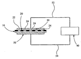
- a wafer 10 of lithium niobate which has been doped with a metal.
- the metal may be an alkaline earth metal such for example as magnesium, or a transition metal such for example as zinc or hafnium.
- the doping is to reduce photorefractive damage.
- the wafer 10 may be of a composition which is congruent or stiochiometric.
- the wafer 10 is typically a z-cut sample.
- the wafer 10 is in the form of a disc, with a thickness of 500 microns, but which may increase up to a few mm in thickness.
- the lateral size of the wafer 10 is chosen to prevent electrical breakdown occurring around the wafer 10. The prevention of this electrical breakdown may typically require that the wafer 10 is at least 5mm larger than the desired poled grating.
- the wafer 10 may be, for example, 7.62 cm.
- An electrode structure 20 is defined by photolithography on the - z face of the wafer 10. More specifically, photoresist 22 is applied to the - z face of the wafer 10 in order to create a series of openings 24 in photoresist 22. An electrode 30 is then deposited over the photoresist 22 as shown, with the material of the electrode 30 extending into the openings 24 and contacting the - z face of the wafer 10.
- the electrode 30 is preferably a gel but it may alternatively be a liquid or a metal. Preferably the electrode 30 is a conductive gel.
- a high voltage supply 40 provides a programmed high voltage which is programmed by an external means such for example as a computer or a signal generator. When the voltage is pulsed, the exposed parts of the wafer 10 are poled.
- an electrode 50 is also shown in the drawing.
- the electrode 50 is typically plain with no pattern.
- the electrode 50 is applied to the + z face of the wafer 10.
- the electrode 50 is made of the same material as the electrode 30.
- the electrodes 30, 50 are connected to the high voltage supply 40 by leads 52, 54 as shown.
- the lithium niobate could alternatively be doped with a transition metal such for example as zinc or hafnium.
- the electrode material may be a liquid or a metal instead of the gel.
- Other sizes of lithium niobate crystal may be employed.
- Crystals of a ferroelectric material other than lithium niobate may be employed so that, for example, the crystal may be a lithium tantalate crystal or a potassium-titanyl-phosphate crystal.
- the photolithography may be applied on the + z face of the wafer 10.
- Various electrode configurations may be used.
Landscapes
- Physics & Mathematics (AREA)
- Nonlinear Science (AREA)
- General Physics & Mathematics (AREA)
- Optics & Photonics (AREA)
- Crystals, And After-Treatments Of Crystals (AREA)
- Optical Modulation, Optical Deflection, Nonlinear Optics, Optical Demodulation, Optical Logic Elements (AREA)
Claims (11)
- Prozess zum Polen eines mit einem Metall dotierten ferroelektrischen Materials (10), wobei der Prozess Folgendes umfasst:(i) definieren eines Elektrodenmusters (20) auf einer -z-Fläche eines Kristalls des mit dem Metall dotierten ferroelektrischen Materials;(ii) Bereitstellen eines Elektrodenmaterials (30);(iii) Polen bei einer Temperatur von höchstens 45°C und(iv) Polen durch ein zweistufiges spannungsgesteuertes Anlegen eines elektrischen Felds an die Elektroden auf der Basis einer ersten Polstufe, wo eine Spannung angelegt wird, um eine Domänenbildung zu erzielen, und einer zweiten Polstufe, wo eine Spannung angelegt wird, um eine Domänenverbreitung zu fördern.
- Prozess nach Anspruch 1, bei dem das Elektrodenmuster (20) ein periodisches Elektrodenmuster ist.
- Prozess nach Anspruch 1 oder 2, bei dem das ferroelektrische Material (10) Lithiumniobat, Lithiumtantalat oder Kaliumtitanylposphat ist.
- Prozess nach einem der vorhergehenden Ansprüche, bei dem das Metall ein Erdalkalimetall oder ein Übergangsmetall ist.
- Prozess nach Anspruch 4, bei dem das Erdalkalimetall Magnesium ist.
- Prozess nach Anspruch 5, bei dem der Kristall des ferroelektrischen Materials (10) mit mehr als 4 Mol-% des Magnesiums dotiert ist.
- Prozess nach Anspruch 4, bei dem das Übergangsmetall Zink oder Hafnium ist.
- Prozess nach einem der vorhergehenden Ansprüche, bei dem die erste Polstufe der Domänenbildung eine Reihe von mehr als einen Impuls unter Verwendung von Spannungen von 8-10 kV/mm und eine Impulsdauer von 1-10 ms mit einem Ein/Aus-Zyklus umfasst, wobei die Zeit, während der der Impuls ausgeschaltet ist, länger ist als 50%.
- Prozess nach einem der vorhergehenden Ansprüche, bei dem die zweite Polstufe der Domänenverbreitung eine Reihe von einem oder mehreren Impulsen von 3-5 kV/mm mit einer Dauer von 1-100 Minuten umfasst.
- Prozess nach einem der vorhergehenden Ansprüche, bei dem das Elektrodenmaterial (30) in der Form eines Gels, einer Flüssigkeit oder eines Metalls vorliegt.
- Prozess nach Anspruch 10, bei dem das Gel ein Lithiumchloridgel oder ein Gel auf der Basis eines organischen Ions ist und bei dem die Flüssigkeit eine Lithiumchloridflüssigkeit ist.
Applications Claiming Priority (2)
| Application Number | Priority Date | Filing Date | Title |
|---|---|---|---|
| GBGB0802852.4A GB0802852D0 (en) | 2008-02-15 | 2008-02-15 | A process for poling a ferroelectric material doped with a metal |
| PCT/GB2009/000358 WO2009101390A1 (en) | 2008-02-15 | 2009-02-09 | A process for poling a ferroelectric material doped with a metal |
Publications (2)
| Publication Number | Publication Date |
|---|---|
| EP2247981A1 EP2247981A1 (de) | 2010-11-10 |
| EP2247981B1 true EP2247981B1 (de) | 2016-06-29 |
Family
ID=39271802
Family Applications (1)
| Application Number | Title | Priority Date | Filing Date |
|---|---|---|---|
| EP09711493.8A Active EP2247981B1 (de) | 2008-02-15 | 2009-02-09 | Verfahren zur polarisierung eines mit einem metall dotierten ferroelektrischen materials |
Country Status (6)
| Country | Link |
|---|---|
| US (1) | US8064129B2 (de) |
| EP (1) | EP2247981B1 (de) |
| JP (1) | JP2011514552A (de) |
| CN (1) | CN101932971B (de) |
| GB (1) | GB0802852D0 (de) |
| WO (1) | WO2009101390A1 (de) |
Families Citing this family (10)
| Publication number | Priority date | Publication date | Assignee | Title |
|---|---|---|---|---|
| JP2010224235A (ja) * | 2009-03-24 | 2010-10-07 | Ngk Insulators Ltd | 波長変換素子 |
| JP5672529B2 (ja) * | 2010-09-13 | 2015-02-18 | 株式会社リコー | 電気光学素子及びその製造方法、並びに、電気光学素子を用いた光偏向装置 |
| CN102122105A (zh) * | 2011-03-15 | 2011-07-13 | 中国科学院半导体研究所 | 一种铁电晶体材料的极化方法 |
| CN106283194B (zh) * | 2016-08-29 | 2018-07-17 | 南开大学 | 一种铌酸锂晶体纳米畴结构的制备装置及方法 |
| CN106736936A (zh) * | 2016-12-02 | 2017-05-31 | 浙江工业大学 | 一种基于施加脉冲磁场的铁电材料减薄加工方法 |
| CN107561817A (zh) * | 2017-10-13 | 2018-01-09 | 上海交通大学 | 铌酸锂薄膜纳米级周期性极化的方法 |
| CN108166065A (zh) * | 2017-12-12 | 2018-06-15 | 南京大学 | 一种制备铌酸锂晶体薄膜畴结构的方法 |
| GB2584877B (en) | 2019-06-19 | 2023-02-08 | Univ Southampton | Method for fabrication of ridge waveguides |
| US11545506B2 (en) | 2020-11-13 | 2023-01-03 | Sandisk Technologies Llc | Ferroelectric field effect transistors having enhanced memory window and methods of making the same |
| US11996462B2 (en) | 2020-11-13 | 2024-05-28 | Sandisk Technologies Llc | Ferroelectric field effect transistors having enhanced memory window and methods of making the same |
Family Cites Families (12)
| Publication number | Priority date | Publication date | Assignee | Title |
|---|---|---|---|---|
| US5519802A (en) * | 1994-05-09 | 1996-05-21 | Deacon Research | Method for making devices having a pattern poled structure and pattern poled structure devices |
| US6555293B1 (en) * | 1998-12-14 | 2003-04-29 | The Board Of Trustees Of The Leland Stanford Junior University | Method for fabricating efficient sources of electromagnetic radiation |
| JP2001242498A (ja) * | 2000-02-28 | 2001-09-07 | Fuji Photo Film Co Ltd | 強誘電体の分極反転方法、並びに光波長変換素子およびその作製方法 |
| JP2001330866A (ja) * | 2000-05-22 | 2001-11-30 | Fuji Photo Film Co Ltd | 光波長変換素子の製造方法 |
| JP4257716B2 (ja) * | 2000-07-14 | 2009-04-22 | 日本碍子株式会社 | 分極反転部の製造方法 |
| GB0115657D0 (en) * | 2001-06-27 | 2001-08-15 | Univ Southampton | High quality surface engineering of domain structures in congruent lithium niobate single crystals |
| JP2004246332A (ja) * | 2002-11-25 | 2004-09-02 | Matsushita Electric Ind Co Ltd | 分極反転構造の形成方法および分極反転構造を有する光学素子 |
| JP4243995B2 (ja) * | 2003-08-21 | 2009-03-25 | 日本碍子株式会社 | 分極反転部の製造方法および光デバイス |
| US7413635B2 (en) * | 2003-12-19 | 2008-08-19 | Spectralus, Inc. | Method for the fabrication of periodically poled Lithium Niobate and Lithium Tantalate nonlinear optical components |
| US7145714B2 (en) * | 2004-07-26 | 2006-12-05 | Advr, Inc. | Segmented electrodes for poling of ferroelectric crystal materials |
| EP1860491A4 (de) * | 2005-03-18 | 2009-07-22 | Nippon Telegraph & Telephone | Herstellungsverfahren für eine periodisch gepolte struktur |
| US7486432B2 (en) * | 2007-03-08 | 2009-02-03 | Hc Photonics Corp. | Method for preparing a periodically poled structure |
-
2008
- 2008-02-15 GB GBGB0802852.4A patent/GB0802852D0/en not_active Ceased
-
2009
- 2009-02-09 WO PCT/GB2009/000358 patent/WO2009101390A1/en not_active Ceased
- 2009-02-09 US US12/735,478 patent/US8064129B2/en active Active
- 2009-02-09 CN CN200980103954.2A patent/CN101932971B/zh active Active
- 2009-02-09 JP JP2010546390A patent/JP2011514552A/ja active Pending
- 2009-02-09 EP EP09711493.8A patent/EP2247981B1/de active Active
Non-Patent Citations (1)
| Title |
|---|
| None * |
Also Published As
| Publication number | Publication date |
|---|---|
| CN101932971B (zh) | 2013-06-12 |
| EP2247981A1 (de) | 2010-11-10 |
| GB0802852D0 (en) | 2008-03-26 |
| JP2011514552A (ja) | 2011-05-06 |
| CN101932971A (zh) | 2010-12-29 |
| US20100288983A1 (en) | 2010-11-18 |
| WO2009101390A1 (en) | 2009-08-20 |
| US8064129B2 (en) | 2011-11-22 |
Similar Documents
| Publication | Publication Date | Title |
|---|---|---|
| US8064129B2 (en) | Process for poling a ferroelectric material doped with a metal | |
| Batchko et al. | Backswitch poling in lithium niobate for high-fidelity domain patterning and efficient blue light generation | |
| Zhu et al. | LiTaO3 crystal periodically poled by applying an external pulsed field | |
| Shur | Kinetics of ferroelectric domains: Application of general approach to LiNbO3 and LiTaO3 | |
| Shur et al. | Recent achievements in domain engineering in lithium niobate and lithium tantalate | |
| EP0745883A1 (de) | Verfahren zur Invertierung von ferroelektrischen Domänen durch Anlegen eines elektrischen Feldes | |
| WO2008152377A1 (en) | Improved electric field poling of ferroelectric materials | |
| US7413635B2 (en) | Method for the fabrication of periodically poled Lithium Niobate and Lithium Tantalate nonlinear optical components | |
| US6654529B1 (en) | Ferroelectric domain inverted waveguide structure and a method for producing a ferroelectric domain inverted waveguide structure | |
| WO2003003111A1 (en) | Electric field poling of ferroelectric materials | |
| JP5300664B2 (ja) | 分極反転部分の製造方法 | |
| Horikawa et al. | Formation of domain-inverted grating in MgO: LiNbO3 by voltage application with insulation layer cladding | |
| US20050084199A1 (en) | Ferroelectric substrate period polarization structure manufacturing method | |
| Shur et al. | Micro-and nanoscale domain engineering in lithium niobate and lithium tantalate | |
| JPH10246900A (ja) | 強誘電体単結晶基板の微小構造の製造方法 | |
| HK1152758A (en) | A process for poling a ferroelectric material doped with a metal | |
| JP4646150B2 (ja) | 周期分極反転構造の製造方法 | |
| JP2003195377A (ja) | 強誘電体の分極反転方法および光波長変換素子の作製方法 | |
| Kwon et al. | Influence of annealing temperature on domain shape of periodically poled LiNbO3 for Ti: LN waveguides | |
| Ghambaryan et al. | Periodically poled structures in lithium niobate crystals: Growth and photoelectric properties | |
| Batchko et al. | Domain patterning in lithium niobate using spontaneous backswitching | |
| JP2004029348A (ja) | 光部品用基材への低抵抗部の形成方法、光部品用基材および光部品 | |
| JP2002214655A (ja) | 強誘電体の分極反転方法および光波長変換素子の作製方法 | |
| Baron et al. | Periodic domain inversion in ion-exchanged LiTaO3 by electric field application | |
| Field et al. | Fabrication of bulk and waveguide PPLN for the generation of wavelengths from 460nm to 4.3 micron |
Legal Events
| Date | Code | Title | Description |
|---|---|---|---|
| PUAI | Public reference made under article 153(3) epc to a published international application that has entered the european phase |
Free format text: ORIGINAL CODE: 0009012 |
|
| 17P | Request for examination filed |
Effective date: 20100624 |
|
| AK | Designated contracting states |
Kind code of ref document: A1 Designated state(s): AT BE BG CH CY CZ DE DK EE ES FI FR GB GR HR HU IE IS IT LI LT LU LV MC MK MT NL NO PL PT RO SE SI SK TR |
|
| AX | Request for extension of the european patent |
Extension state: AL BA RS |
|
| 17Q | First examination report despatched |
Effective date: 20110204 |
|
| DAX | Request for extension of the european patent (deleted) | ||
| GRAP | Despatch of communication of intention to grant a patent |
Free format text: ORIGINAL CODE: EPIDOSNIGR1 |
|
| INTG | Intention to grant announced |
Effective date: 20151116 |
|
| GRAP | Despatch of communication of intention to grant a patent |
Free format text: ORIGINAL CODE: EPIDOSNIGR1 |
|
| INTG | Intention to grant announced |
Effective date: 20160311 |
|
| RIN1 | Information on inventor provided before grant (corrected) |
Inventor name: GAWITH, CORIN BARRY EDMUND Inventor name: MAJOR, HUW EDWARD Inventor name: SMITH, PETER GEORGE ROBIN |
|
| GRAS | Grant fee paid |
Free format text: ORIGINAL CODE: EPIDOSNIGR3 |
|
| GRAA | (expected) grant |
Free format text: ORIGINAL CODE: 0009210 |
|
| AK | Designated contracting states |
Kind code of ref document: B1 Designated state(s): AT BE BG CH CY CZ DE DK EE ES FI FR GB GR HR HU IE IS IT LI LT LU LV MC MK MT NL NO PL PT RO SE SI SK TR |
|
| REG | Reference to a national code |
Ref country code: GB Ref legal event code: FG4D |
|
| REG | Reference to a national code |
Ref country code: CH Ref legal event code: EP |
|
| REG | Reference to a national code |
Ref country code: AT Ref legal event code: REF Ref document number: 809555 Country of ref document: AT Kind code of ref document: T Effective date: 20160715 |
|
| REG | Reference to a national code |
Ref country code: IE Ref legal event code: FG4D |
|
| REG | Reference to a national code |
Ref country code: DE Ref legal event code: R096 Ref document number: 602009039439 Country of ref document: DE |
|
| REG | Reference to a national code |
Ref country code: LT Ref legal event code: MG4D |
|
| PG25 | Lapsed in a contracting state [announced via postgrant information from national office to epo] |
Ref country code: FI Free format text: LAPSE BECAUSE OF FAILURE TO SUBMIT A TRANSLATION OF THE DESCRIPTION OR TO PAY THE FEE WITHIN THE PRESCRIBED TIME-LIMIT Effective date: 20160629 Ref country code: LT Free format text: LAPSE BECAUSE OF FAILURE TO SUBMIT A TRANSLATION OF THE DESCRIPTION OR TO PAY THE FEE WITHIN THE PRESCRIBED TIME-LIMIT Effective date: 20160629 Ref country code: NO Free format text: LAPSE BECAUSE OF FAILURE TO SUBMIT A TRANSLATION OF THE DESCRIPTION OR TO PAY THE FEE WITHIN THE PRESCRIBED TIME-LIMIT Effective date: 20160929 |
|
| REG | Reference to a national code |
Ref country code: NL Ref legal event code: MP Effective date: 20160629 |
|
| PG25 | Lapsed in a contracting state [announced via postgrant information from national office to epo] |
Ref country code: LV Free format text: LAPSE BECAUSE OF FAILURE TO SUBMIT A TRANSLATION OF THE DESCRIPTION OR TO PAY THE FEE WITHIN THE PRESCRIBED TIME-LIMIT Effective date: 20160629 Ref country code: NL Free format text: LAPSE BECAUSE OF FAILURE TO SUBMIT A TRANSLATION OF THE DESCRIPTION OR TO PAY THE FEE WITHIN THE PRESCRIBED TIME-LIMIT Effective date: 20160629 Ref country code: HR Free format text: LAPSE BECAUSE OF FAILURE TO SUBMIT A TRANSLATION OF THE DESCRIPTION OR TO PAY THE FEE WITHIN THE PRESCRIBED TIME-LIMIT Effective date: 20160629 Ref country code: SE Free format text: LAPSE BECAUSE OF FAILURE TO SUBMIT A TRANSLATION OF THE DESCRIPTION OR TO PAY THE FEE WITHIN THE PRESCRIBED TIME-LIMIT Effective date: 20160629 Ref country code: GR Free format text: LAPSE BECAUSE OF FAILURE TO SUBMIT A TRANSLATION OF THE DESCRIPTION OR TO PAY THE FEE WITHIN THE PRESCRIBED TIME-LIMIT Effective date: 20160930 |
|
| REG | Reference to a national code |
Ref country code: AT Ref legal event code: MK05 Ref document number: 809555 Country of ref document: AT Kind code of ref document: T Effective date: 20160629 |
|
| PG25 | Lapsed in a contracting state [announced via postgrant information from national office to epo] |
Ref country code: RO Free format text: LAPSE BECAUSE OF FAILURE TO SUBMIT A TRANSLATION OF THE DESCRIPTION OR TO PAY THE FEE WITHIN THE PRESCRIBED TIME-LIMIT Effective date: 20160629 Ref country code: IS Free format text: LAPSE BECAUSE OF FAILURE TO SUBMIT A TRANSLATION OF THE DESCRIPTION OR TO PAY THE FEE WITHIN THE PRESCRIBED TIME-LIMIT Effective date: 20161029 Ref country code: SK Free format text: LAPSE BECAUSE OF FAILURE TO SUBMIT A TRANSLATION OF THE DESCRIPTION OR TO PAY THE FEE WITHIN THE PRESCRIBED TIME-LIMIT Effective date: 20160629 Ref country code: CZ Free format text: LAPSE BECAUSE OF FAILURE TO SUBMIT A TRANSLATION OF THE DESCRIPTION OR TO PAY THE FEE WITHIN THE PRESCRIBED TIME-LIMIT Effective date: 20160629 Ref country code: IT Free format text: LAPSE BECAUSE OF FAILURE TO SUBMIT A TRANSLATION OF THE DESCRIPTION OR TO PAY THE FEE WITHIN THE PRESCRIBED TIME-LIMIT Effective date: 20160629 Ref country code: EE Free format text: LAPSE BECAUSE OF FAILURE TO SUBMIT A TRANSLATION OF THE DESCRIPTION OR TO PAY THE FEE WITHIN THE PRESCRIBED TIME-LIMIT Effective date: 20160629 |
|
| REG | Reference to a national code |
Ref country code: FR Ref legal event code: PLFP Year of fee payment: 9 |
|
| PG25 | Lapsed in a contracting state [announced via postgrant information from national office to epo] |
Ref country code: ES Free format text: LAPSE BECAUSE OF FAILURE TO SUBMIT A TRANSLATION OF THE DESCRIPTION OR TO PAY THE FEE WITHIN THE PRESCRIBED TIME-LIMIT Effective date: 20160629 Ref country code: PL Free format text: LAPSE BECAUSE OF FAILURE TO SUBMIT A TRANSLATION OF THE DESCRIPTION OR TO PAY THE FEE WITHIN THE PRESCRIBED TIME-LIMIT Effective date: 20160629 Ref country code: PT Free format text: LAPSE BECAUSE OF FAILURE TO SUBMIT A TRANSLATION OF THE DESCRIPTION OR TO PAY THE FEE WITHIN THE PRESCRIBED TIME-LIMIT Effective date: 20161031 Ref country code: BE Free format text: LAPSE BECAUSE OF FAILURE TO SUBMIT A TRANSLATION OF THE DESCRIPTION OR TO PAY THE FEE WITHIN THE PRESCRIBED TIME-LIMIT Effective date: 20160629 Ref country code: AT Free format text: LAPSE BECAUSE OF FAILURE TO SUBMIT A TRANSLATION OF THE DESCRIPTION OR TO PAY THE FEE WITHIN THE PRESCRIBED TIME-LIMIT Effective date: 20160629 |
|
| REG | Reference to a national code |
Ref country code: DE Ref legal event code: R097 Ref document number: 602009039439 Country of ref document: DE |
|
| PLBE | No opposition filed within time limit |
Free format text: ORIGINAL CODE: 0009261 |
|
| STAA | Information on the status of an ep patent application or granted ep patent |
Free format text: STATUS: NO OPPOSITION FILED WITHIN TIME LIMIT |
|
| PG25 | Lapsed in a contracting state [announced via postgrant information from national office to epo] |
Ref country code: DK Free format text: LAPSE BECAUSE OF FAILURE TO SUBMIT A TRANSLATION OF THE DESCRIPTION OR TO PAY THE FEE WITHIN THE PRESCRIBED TIME-LIMIT Effective date: 20160629 |
|
| 26N | No opposition filed |
Effective date: 20170330 |
|
| PG25 | Lapsed in a contracting state [announced via postgrant information from national office to epo] |
Ref country code: BG Free format text: LAPSE BECAUSE OF FAILURE TO SUBMIT A TRANSLATION OF THE DESCRIPTION OR TO PAY THE FEE WITHIN THE PRESCRIBED TIME-LIMIT Effective date: 20160929 Ref country code: SI Free format text: LAPSE BECAUSE OF FAILURE TO SUBMIT A TRANSLATION OF THE DESCRIPTION OR TO PAY THE FEE WITHIN THE PRESCRIBED TIME-LIMIT Effective date: 20160629 |
|
| PG25 | Lapsed in a contracting state [announced via postgrant information from national office to epo] |
Ref country code: MC Free format text: LAPSE BECAUSE OF FAILURE TO SUBMIT A TRANSLATION OF THE DESCRIPTION OR TO PAY THE FEE WITHIN THE PRESCRIBED TIME-LIMIT Effective date: 20160629 |
|
| REG | Reference to a national code |
Ref country code: CH Ref legal event code: PL |
|
| PG25 | Lapsed in a contracting state [announced via postgrant information from national office to epo] |
Ref country code: LI Free format text: LAPSE BECAUSE OF NON-PAYMENT OF DUE FEES Effective date: 20170228 Ref country code: CH Free format text: LAPSE BECAUSE OF NON-PAYMENT OF DUE FEES Effective date: 20170228 |
|
| REG | Reference to a national code |
Ref country code: IE Ref legal event code: MM4A |
|
| PG25 | Lapsed in a contracting state [announced via postgrant information from national office to epo] |
Ref country code: LU Free format text: LAPSE BECAUSE OF NON-PAYMENT OF DUE FEES Effective date: 20170209 |
|
| REG | Reference to a national code |
Ref country code: FR Ref legal event code: PLFP Year of fee payment: 10 |
|
| PG25 | Lapsed in a contracting state [announced via postgrant information from national office to epo] |
Ref country code: IE Free format text: LAPSE BECAUSE OF NON-PAYMENT OF DUE FEES Effective date: 20170209 |
|
| PG25 | Lapsed in a contracting state [announced via postgrant information from national office to epo] |
Ref country code: MT Free format text: LAPSE BECAUSE OF NON-PAYMENT OF DUE FEES Effective date: 20170209 |
|
| PG25 | Lapsed in a contracting state [announced via postgrant information from national office to epo] |
Ref country code: HU Free format text: LAPSE BECAUSE OF FAILURE TO SUBMIT A TRANSLATION OF THE DESCRIPTION OR TO PAY THE FEE WITHIN THE PRESCRIBED TIME-LIMIT; INVALID AB INITIO Effective date: 20090209 |
|
| PG25 | Lapsed in a contracting state [announced via postgrant information from national office to epo] |
Ref country code: CY Free format text: LAPSE BECAUSE OF NON-PAYMENT OF DUE FEES Effective date: 20160629 |
|
| PG25 | Lapsed in a contracting state [announced via postgrant information from national office to epo] |
Ref country code: MK Free format text: LAPSE BECAUSE OF FAILURE TO SUBMIT A TRANSLATION OF THE DESCRIPTION OR TO PAY THE FEE WITHIN THE PRESCRIBED TIME-LIMIT Effective date: 20160629 |
|
| PG25 | Lapsed in a contracting state [announced via postgrant information from national office to epo] |
Ref country code: TR Free format text: LAPSE BECAUSE OF FAILURE TO SUBMIT A TRANSLATION OF THE DESCRIPTION OR TO PAY THE FEE WITHIN THE PRESCRIBED TIME-LIMIT Effective date: 20160629 |
|
| PGFP | Annual fee paid to national office [announced via postgrant information from national office to epo] |
Ref country code: GB Payment date: 20260219 Year of fee payment: 18 |
|
| PGFP | Annual fee paid to national office [announced via postgrant information from national office to epo] |
Ref country code: DE Payment date: 20260218 Year of fee payment: 18 |
|
| PGFP | Annual fee paid to national office [announced via postgrant information from national office to epo] |
Ref country code: FR Payment date: 20260218 Year of fee payment: 18 |