EP2238606B1 - Balayage de faisceaux de particules chargées - Google Patents
Balayage de faisceaux de particules chargées Download PDFInfo
- Publication number
- EP2238606B1 EP2238606B1 EP08862809A EP08862809A EP2238606B1 EP 2238606 B1 EP2238606 B1 EP 2238606B1 EP 08862809 A EP08862809 A EP 08862809A EP 08862809 A EP08862809 A EP 08862809A EP 2238606 B1 EP2238606 B1 EP 2238606B1
- Authority
- EP
- European Patent Office
- Prior art keywords
- sample
- ion beam
- less
- portions
- region
- Prior art date
- Legal status (The legal status is an assumption and is not a legal conclusion. Google has not performed a legal analysis and makes no representation as to the accuracy of the status listed.)
- Active
Links
- 239000002245 particle Substances 0.000 title claims abstract description 247
- 238000000034 method Methods 0.000 claims abstract description 119
- 150000002500 ions Chemical class 0.000 claims description 274
- 230000007935 neutral effect Effects 0.000 claims description 35
- 238000010438 heat treatment Methods 0.000 claims description 5
- 239000000523 sample Substances 0.000 description 459
- 238000010884 ion-beam technique Methods 0.000 description 365
- 239000007789 gas Substances 0.000 description 118
- 230000000875 corresponding effect Effects 0.000 description 39
- 239000000463 material Substances 0.000 description 37
- 239000010931 gold Substances 0.000 description 31
- 230000003993 interaction Effects 0.000 description 30
- 230000005684 electric field Effects 0.000 description 29
- PCHJSUWPFVWCPO-UHFFFAOYSA-N gold Chemical compound [Au] PCHJSUWPFVWCPO-UHFFFAOYSA-N 0.000 description 29
- 229910052737 gold Inorganic materials 0.000 description 28
- 229910052734 helium Inorganic materials 0.000 description 26
- 230000002829 reductive effect Effects 0.000 description 24
- 238000005259 measurement Methods 0.000 description 22
- 238000010894 electron beam technology Methods 0.000 description 20
- 239000001307 helium Substances 0.000 description 18
- 229910052756 noble gas Inorganic materials 0.000 description 18
- 238000010586 diagram Methods 0.000 description 17
- 238000009792 diffusion process Methods 0.000 description 16
- -1 helium ions Chemical class 0.000 description 16
- 230000001965 increasing effect Effects 0.000 description 16
- OKTJSMMVPCPJKN-UHFFFAOYSA-N Carbon Chemical compound [C] OKTJSMMVPCPJKN-UHFFFAOYSA-N 0.000 description 15
- 229910052799 carbon Inorganic materials 0.000 description 15
- 239000013043 chemical agent Substances 0.000 description 15
- 238000006243 chemical reaction Methods 0.000 description 15
- 238000003384 imaging method Methods 0.000 description 14
- IJGRMHOSHXDMSA-UHFFFAOYSA-N Atomic nitrogen Chemical compound N#N IJGRMHOSHXDMSA-UHFFFAOYSA-N 0.000 description 12
- 238000012935 Averaging Methods 0.000 description 12
- 238000013519 translation Methods 0.000 description 12
- 230000014616 translation Effects 0.000 description 12
- 238000001514 detection method Methods 0.000 description 10
- 230000006870 function Effects 0.000 description 10
- SWQJXJOGLNCZEY-UHFFFAOYSA-N helium atom Chemical compound [He] SWQJXJOGLNCZEY-UHFFFAOYSA-N 0.000 description 10
- 239000013638 trimer Substances 0.000 description 10
- 230000008569 process Effects 0.000 description 9
- 239000007787 solid Substances 0.000 description 9
- 239000013078 crystal Substances 0.000 description 8
- 238000009826 distribution Methods 0.000 description 8
- 230000000694 effects Effects 0.000 description 8
- 230000003287 optical effect Effects 0.000 description 8
- OAICVXFJPJFONN-UHFFFAOYSA-N Phosphorus Chemical compound [P] OAICVXFJPJFONN-UHFFFAOYSA-N 0.000 description 7
- 229910052751 metal Inorganic materials 0.000 description 7
- 239000002184 metal Substances 0.000 description 7
- 230000004044 response Effects 0.000 description 7
- 239000004065 semiconductor Substances 0.000 description 7
- 230000004907 flux Effects 0.000 description 6
- 238000002513 implantation Methods 0.000 description 6
- 239000000203 mixture Substances 0.000 description 6
- 238000004544 sputter deposition Methods 0.000 description 6
- 230000008901 benefit Effects 0.000 description 5
- 239000013626 chemical specie Substances 0.000 description 5
- 239000004020 conductor Substances 0.000 description 5
- 230000001419 dependent effect Effects 0.000 description 5
- CKHJYUSOUQDYEN-UHFFFAOYSA-N gallium(3+) Chemical compound [Ga+3] CKHJYUSOUQDYEN-UHFFFAOYSA-N 0.000 description 5
- 229910052757 nitrogen Inorganic materials 0.000 description 5
- BASFCYQUMIYNBI-UHFFFAOYSA-N platinum Chemical compound [Pt] BASFCYQUMIYNBI-UHFFFAOYSA-N 0.000 description 5
- 230000010287 polarization Effects 0.000 description 5
- 239000000047 product Substances 0.000 description 5
- 238000003860 storage Methods 0.000 description 5
- 239000000758 substrate Substances 0.000 description 5
- XUIMIQQOPSSXEZ-UHFFFAOYSA-N Silicon Chemical compound [Si] XUIMIQQOPSSXEZ-UHFFFAOYSA-N 0.000 description 4
- 230000015572 biosynthetic process Effects 0.000 description 4
- 238000004590 computer program Methods 0.000 description 4
- 239000010949 copper Substances 0.000 description 4
- 230000002596 correlated effect Effects 0.000 description 4
- 238000001493 electron microscopy Methods 0.000 description 4
- 239000012535 impurity Substances 0.000 description 4
- 238000012986 modification Methods 0.000 description 4
- 230000004048 modification Effects 0.000 description 4
- 238000010943 off-gassing Methods 0.000 description 4
- 229910052710 silicon Inorganic materials 0.000 description 4
- 239000010703 silicon Substances 0.000 description 4
- 238000012360 testing method Methods 0.000 description 4
- 230000003213 activating effect Effects 0.000 description 3
- 238000004458 analytical method Methods 0.000 description 3
- 239000000470 constituent Substances 0.000 description 3
- 230000000116 mitigating effect Effects 0.000 description 3
- 230000008439 repair process Effects 0.000 description 3
- XKRFYHLGVUSROY-UHFFFAOYSA-N Argon Chemical compound [Ar] XKRFYHLGVUSROY-UHFFFAOYSA-N 0.000 description 2
- VYZAMTAEIAYCRO-UHFFFAOYSA-N Chromium Chemical compound [Cr] VYZAMTAEIAYCRO-UHFFFAOYSA-N 0.000 description 2
- XEEYBQQBJWHFJM-UHFFFAOYSA-N Iron Chemical compound [Fe] XEEYBQQBJWHFJM-UHFFFAOYSA-N 0.000 description 2
- 238000009825 accumulation Methods 0.000 description 2
- 229910045601 alloy Inorganic materials 0.000 description 2
- 239000000956 alloy Substances 0.000 description 2
- 201000009310 astigmatism Diseases 0.000 description 2
- 238000004364 calculation method Methods 0.000 description 2
- 230000015556 catabolic process Effects 0.000 description 2
- 230000008859 change Effects 0.000 description 2
- 239000003795 chemical substances by application Substances 0.000 description 2
- 230000001276 controlling effect Effects 0.000 description 2
- 230000003247 decreasing effect Effects 0.000 description 2
- 238000006731 degradation reaction Methods 0.000 description 2
- 229910001873 dinitrogen Inorganic materials 0.000 description 2
- 239000003574 free electron Substances 0.000 description 2
- 230000001976 improved effect Effects 0.000 description 2
- 238000005468 ion implantation Methods 0.000 description 2
- 238000005304 joining Methods 0.000 description 2
- 229910052743 krypton Inorganic materials 0.000 description 2
- 239000007788 liquid Substances 0.000 description 2
- 238000004519 manufacturing process Methods 0.000 description 2
- 229910052754 neon Inorganic materials 0.000 description 2
- 239000010955 niobium Substances 0.000 description 2
- 229910052697 platinum Inorganic materials 0.000 description 2
- 239000002243 precursor Substances 0.000 description 2
- 239000011163 secondary particle Substances 0.000 description 2
- 238000007740 vapor deposition Methods 0.000 description 2
- 229910052724 xenon Inorganic materials 0.000 description 2
- IGELFKKMDLGCJO-UHFFFAOYSA-N xenon difluoride Chemical compound F[Xe]F IGELFKKMDLGCJO-UHFFFAOYSA-N 0.000 description 2
- NCGICGYLBXGBGN-UHFFFAOYSA-N 3-morpholin-4-yl-1-oxa-3-azonia-2-azanidacyclopent-3-en-5-imine;hydrochloride Chemical compound Cl.[N-]1OC(=N)C=[N+]1N1CCOCC1 NCGICGYLBXGBGN-UHFFFAOYSA-N 0.000 description 1
- 239000004215 Carbon black (E152) Substances 0.000 description 1
- RYGMFSIKBFXOCR-UHFFFAOYSA-N Copper Chemical compound [Cu] RYGMFSIKBFXOCR-UHFFFAOYSA-N 0.000 description 1
- ZOKXTWBITQBERF-UHFFFAOYSA-N Molybdenum Chemical compound [Mo] ZOKXTWBITQBERF-UHFFFAOYSA-N 0.000 description 1
- VYPSYNLAJGMNEJ-UHFFFAOYSA-N Silicium dioxide Chemical compound O=[Si]=O VYPSYNLAJGMNEJ-UHFFFAOYSA-N 0.000 description 1
- 230000003321 amplification Effects 0.000 description 1
- 238000013459 approach Methods 0.000 description 1
- 229910052786 argon Inorganic materials 0.000 description 1
- 238000003491 array Methods 0.000 description 1
- 230000004397 blinking Effects 0.000 description 1
- 239000006227 byproduct Substances 0.000 description 1
- 238000004891 communication Methods 0.000 description 1
- 230000001010 compromised effect Effects 0.000 description 1
- 238000011109 contamination Methods 0.000 description 1
- 239000002826 coolant Substances 0.000 description 1
- 229910052802 copper Inorganic materials 0.000 description 1
- 230000008878 coupling Effects 0.000 description 1
- 238000010168 coupling process Methods 0.000 description 1
- 238000005859 coupling reaction Methods 0.000 description 1
- 230000000254 damaging effect Effects 0.000 description 1
- 230000007547 defect Effects 0.000 description 1
- 230000000593 degrading effect Effects 0.000 description 1
- 238000013461 design Methods 0.000 description 1
- QDOXWKRWXJOMAK-UHFFFAOYSA-N dichromium trioxide Chemical compound O=[Cr]O[Cr]=O QDOXWKRWXJOMAK-UHFFFAOYSA-N 0.000 description 1
- 230000008034 disappearance Effects 0.000 description 1
- 238000000609 electron-beam lithography Methods 0.000 description 1
- 238000005530 etching Methods 0.000 description 1
- 230000008020 evaporation Effects 0.000 description 1
- 238000001704 evaporation Methods 0.000 description 1
- 239000011888 foil Substances 0.000 description 1
- 239000005350 fused silica glass Substances 0.000 description 1
- 230000004927 fusion Effects 0.000 description 1
- 229910052733 gallium Inorganic materials 0.000 description 1
- 229930195733 hydrocarbon Natural products 0.000 description 1
- 150000002430 hydrocarbons Chemical class 0.000 description 1
- 239000001257 hydrogen Substances 0.000 description 1
- 229910052739 hydrogen Inorganic materials 0.000 description 1
- 239000007943 implant Substances 0.000 description 1
- 238000011065 in-situ storage Methods 0.000 description 1
- 230000001939 inductive effect Effects 0.000 description 1
- 238000007689 inspection Methods 0.000 description 1
- 238000000752 ionisation method Methods 0.000 description 1
- 229910052741 iridium Inorganic materials 0.000 description 1
- GKOZUEZYRPOHIO-UHFFFAOYSA-N iridium atom Chemical compound [Ir] GKOZUEZYRPOHIO-UHFFFAOYSA-N 0.000 description 1
- 229910052742 iron Inorganic materials 0.000 description 1
- DNNSSWSSYDEUBZ-UHFFFAOYSA-N krypton atom Chemical compound [Kr] DNNSSWSSYDEUBZ-UHFFFAOYSA-N 0.000 description 1
- 230000000670 limiting effect Effects 0.000 description 1
- 229910001338 liquidmetal Inorganic materials 0.000 description 1
- 238000003754 machining Methods 0.000 description 1
- 230000000873 masking effect Effects 0.000 description 1
- 230000007246 mechanism Effects 0.000 description 1
- 150000002739 metals Chemical class 0.000 description 1
- 229910052750 molybdenum Inorganic materials 0.000 description 1
- 239000011733 molybdenum Substances 0.000 description 1
- GKAOGPIIYCISHV-UHFFFAOYSA-N neon atom Chemical compound [Ne] GKAOGPIIYCISHV-UHFFFAOYSA-N 0.000 description 1
- 229910052758 niobium Inorganic materials 0.000 description 1
- GUCVJGMIXFAOAE-UHFFFAOYSA-N niobium atom Chemical compound [Nb] GUCVJGMIXFAOAE-UHFFFAOYSA-N 0.000 description 1
- 150000002835 noble gases Chemical class 0.000 description 1
- 238000003199 nucleic acid amplification method Methods 0.000 description 1
- 238000005086 pumping Methods 0.000 description 1
- 230000009467 reduction Effects 0.000 description 1
- 229910052702 rhenium Inorganic materials 0.000 description 1
- WUAPFZMCVAUBPE-UHFFFAOYSA-N rhenium atom Chemical compound [Re] WUAPFZMCVAUBPE-UHFFFAOYSA-N 0.000 description 1
- 229920006395 saturated elastomer Polymers 0.000 description 1
- 238000000926 separation method Methods 0.000 description 1
- 238000007493 shaping process Methods 0.000 description 1
- 239000002210 silicon-based material Substances 0.000 description 1
- 238000004088 simulation Methods 0.000 description 1
- 238000001179 sorption measurement Methods 0.000 description 1
- 230000003595 spectral effect Effects 0.000 description 1
- 238000001228 spectrum Methods 0.000 description 1
- 230000001360 synchronised effect Effects 0.000 description 1
- 229910052715 tantalum Inorganic materials 0.000 description 1
- GUVRBAGPIYLISA-UHFFFAOYSA-N tantalum atom Chemical compound [Ta] GUVRBAGPIYLISA-UHFFFAOYSA-N 0.000 description 1
- MZLGASXMSKOWSE-UHFFFAOYSA-N tantalum nitride Chemical compound [Ta]#N MZLGASXMSKOWSE-UHFFFAOYSA-N 0.000 description 1
- 230000002123 temporal effect Effects 0.000 description 1
- 238000012876 topography Methods 0.000 description 1
- 230000007723 transport mechanism Effects 0.000 description 1
- WFKWXMTUELFFGS-UHFFFAOYSA-N tungsten Chemical compound [W] WFKWXMTUELFFGS-UHFFFAOYSA-N 0.000 description 1
- 229910052721 tungsten Inorganic materials 0.000 description 1
- 239000010937 tungsten Substances 0.000 description 1
- 230000005641 tunneling Effects 0.000 description 1
- FHNFHKCVQCLJFQ-UHFFFAOYSA-N xenon atom Chemical compound [Xe] FHNFHKCVQCLJFQ-UHFFFAOYSA-N 0.000 description 1
Images


Classifications
-
- H—ELECTRICITY
- H01—ELECTRIC ELEMENTS
- H01J—ELECTRIC DISCHARGE TUBES OR DISCHARGE LAMPS
- H01J37/00—Discharge tubes with provision for introducing objects or material to be exposed to the discharge, e.g. for the purpose of examination or processing thereof
- H01J37/02—Details
- H01J37/026—Means for avoiding or neutralising unwanted electrical charges on tube components
-
- H—ELECTRICITY
- H01—ELECTRIC ELEMENTS
- H01J—ELECTRIC DISCHARGE TUBES OR DISCHARGE LAMPS
- H01J37/00—Discharge tubes with provision for introducing objects or material to be exposed to the discharge, e.g. for the purpose of examination or processing thereof
- H01J37/26—Electron or ion microscopes; Electron or ion diffraction tubes
- H01J37/28—Electron or ion microscopes; Electron or ion diffraction tubes with scanning beams
-
- H—ELECTRICITY
- H01—ELECTRIC ELEMENTS
- H01J—ELECTRIC DISCHARGE TUBES OR DISCHARGE LAMPS
- H01J37/00—Discharge tubes with provision for introducing objects or material to be exposed to the discharge, e.g. for the purpose of examination or processing thereof
- H01J37/30—Electron-beam or ion-beam tubes for localised treatment of objects
- H01J37/302—Controlling tubes by external information, e.g. programme control
- H01J37/3023—Programme control
- H01J37/3026—Patterning strategy
-
- H—ELECTRICITY
- H01—ELECTRIC ELEMENTS
- H01J—ELECTRIC DISCHARGE TUBES OR DISCHARGE LAMPS
- H01J2237/00—Discharge tubes exposing object to beam, e.g. for analysis treatment, etching, imaging
- H01J2237/004—Charge control of objects or beams
-
- H—ELECTRICITY
- H01—ELECTRIC ELEMENTS
- H01J—ELECTRIC DISCHARGE TUBES OR DISCHARGE LAMPS
- H01J2237/00—Discharge tubes exposing object to beam, e.g. for analysis treatment, etching, imaging
- H01J2237/02—Details
- H01J2237/022—Avoiding or removing foreign or contaminating particles, debris or deposits on sample or tube
-
- H—ELECTRICITY
- H01—ELECTRIC ELEMENTS
- H01J—ELECTRIC DISCHARGE TUBES OR DISCHARGE LAMPS
- H01J2237/00—Discharge tubes exposing object to beam, e.g. for analysis treatment, etching, imaging
- H01J2237/06—Sources
- H01J2237/08—Ion sources
- H01J2237/0802—Field ionization sources
- H01J2237/0807—Gas field ion sources [GFIS]
-
- H—ELECTRICITY
- H01—ELECTRIC ELEMENTS
- H01J—ELECTRIC DISCHARGE TUBES OR DISCHARGE LAMPS
- H01J2237/00—Discharge tubes exposing object to beam, e.g. for analysis treatment, etching, imaging
- H01J2237/30—Electron or ion beam tubes for processing objects
- H01J2237/304—Controlling tubes
- H01J2237/30472—Controlling the beam
- H01J2237/30483—Scanning
- H01J2237/30488—Raster scan
Definitions
- This disclosure relates to charged particle sources, systems, and methods.
- Ions can be formed using, for example, a liquid metal ion source or a gas field ion source.
- ions formed by an ion source can be used to determine certain properties of a sample that is exposed to the ions, or to modify the sample.
- ions formed by an ion source can be used to determine certain characteristics of the ion source itself.
- Document EP-A-1 271 605 discloses a method for thinned out scanning in order to mitigate the problem of surface charging during electron beam imaging.
- Document US 2003/022078 A1 discloses a method for electron beam lithography which comprises the steps of measuring the lengths of the sides of rectangles in a selected region and exposing portions of the region according to the pattern formed by these rectangles.
- Document US-B1-6 566 662 discloses a method for exposing a wafer to an electron beam comprising the steps of determining exposure periods and the length of the portion which are to be exposed in order to calculate the speed of a specimen stage on which the wafer is located.
- a method includes: (a) determining a side length of a smallest square that encloses a region of a sample, where A is an area of the region and F is a constant; and (b) exposing each of M portions of the region of the sample to a charged particle beam, where each of the M portions is exposed continuously to the charged particle beam for a time period t 1 , a shortest time period between successive exposures of any one of the M portions to the charged particle beam is t 2 , and the time periods t 1 and t 2 are selected so that a ratio t 1 t 1 + t 2 is less than 1 2 ⁇ F ⁇ M .
- Embodiments can include one or more of the following features.
- the method can include exposing, in direct succession, a second plurality of portions of the surface of the sample to the charged particle beam, each portion of the second plurality of portions being spaced from its neighboring portions in the second plurality of portions by a distance of at least d in the first direction and being spaced from the first portions by a distance of at least e in a second direction orthogonal to the first direction.
- the sample and the charged particle beam can be positioned within a common chamber having a gas pressure less than 10 -2 Torr, and a plurality of particles leaving the sample can be detected by a detector positioned within the common chamber.
- the sample can be positioned on a sample mount that permits translation of the sample in a plane orthogonal to a direction of incidence of the charged particle beam, and the mount can be configured to permit exchange of the sample for another sample.
- the sample can be positioned on a sample mount, and the sample mount can be configured to permit adjustment of a distance between the sample and a lens of a charged particle lens system that directs that charged particle beam to be incident on the sample.
- a ratio e / f can be 2 or more (e.g., 3 or more, 4 or more, 5 or more, 7 or more, 10 or more, 20 or more, 30 or more, 50 or more, 70 or more, 100 or more).
- the quantity e can be greater than or equal to d .
- the method can include forming an image of the sample based on a plurality of particles leaving the sample.
- the method can include displaying the image of the sample to a system operator on an electronic display unit.
- the method can include exposing the sample to an electron source prior to exposing the sample to the charged particle beam. Alternatively, or in addition, the method can include exposing the sample to an electron source during exposure of the sample to the charged particle beam.
- a charged particle current of the charged particle beam can be 10 pA or more (e.g., 20 pA or more, 30 pA or more, 40 pA or more, 50 pA or more, 70 pA or more, 100 pA or more, 150 pA or more, 200 pA or more, 500 pA or more).
- Each portion can be exposed to the charged particle beam for an exposure time of 100 ⁇ s or less (e.g, 80 ⁇ s or less, 60 ⁇ s or less, 40 ⁇ s or less, 30 ⁇ s or less, 20 ⁇ s or less, 10 ⁇ s or less, 5 ⁇ s or less, 1 ⁇ s or less, 0.5 ⁇ s or less, 0.1 ⁇ s or less).
- 100 ⁇ s or less e.g, 80 ⁇ s or less, 60 ⁇ s or less, 40 ⁇ s or less, 30 ⁇ s or less, 20 ⁇ s or less, 10 ⁇ s or less, 5 ⁇ s or less, 1 ⁇ s or less, 0.5 ⁇ s or less, 0.1 ⁇ s or less.
- a charged particle current of the charged particle beam can be 1 pA or more, each of the portions can be exposed to the charged particle beam for an exposure time of 100 ⁇ s or less, and the image can be formed over a total acquisition time of 100 seconds or less.
- the charged particle beam can include noble gas ions.
- the noble gas ions can include helium ions.
- the charged particle beam can include electrons.
- the value of f can be 5 nm or less (e.g., 4 nm or less, 3 nm or less, 2 nm or less, 1 nm or less, 0.5 nm or less).
- the value of d can be 10 nm or more (e.g., 20 nm or more, 30 nm or more, 40 nm or more, 50 nm or more, 70 nm or more, 100 nm or more, 200 nm or more, 300 nm or more, 500 nm or more).
- the value of e can be 10 nm or more (e.g., 20 nm or more, 30 nm or more, 40 nm or more, 50 nm or more, 70 nm or more, 100 nm or more, 200 nm or more, 300 nm or more, 500 nm or more).
- the charged particle beam can have an energy spread at the surface of the sample of five eV or less (e.g., four eV or less, three eV or less, two eV or less, one eV or less, 0.5 eV or less, 0.1 eV or less).
- five eV or less e.g., four eV or less, three eV or less, two eV or less, one eV or less, 0.5 eV or less, 0.1 eV or less.
- a resolution of the image can be three nm or less (e.g., two nm or less, one nm or less, 0.5 nm or less, 0.25 nm or less, 0.1 nm or less).
- the plurality of particles can include secondary electrons.
- the plurality of particles can include at least one member of the group consisting of scattered ions and scattered neutral atoms.
- the plurality of particles can include photons.
- the charged particle beam can be produced by a gas field ion microscope having a quality factor of 0.25 or more (e.g., a quality factor of 0.5 or more, a quality factor of 1 or more, a quality factor of 2 or more, a quality factor of 3 or more, a quality factor of 5 or more, a quality factor of 10 or more).
- a quality factor of 0.25 or more e.g., a quality factor of 0.5 or more, a quality factor of 1 or more, a quality factor of 2 or more, a quality factor of 3 or more, a quality factor of 5 or more, a quality factor of 10 or more.
- Each of the portions can include multiple image pixels.
- the method can include heating the sample during exposure to the charged particle beam.
- the charged particle beam can have a reduced brightness at the surface of the sample of 5x10 8 A/m 2 srV or more (e.g., 1x10 9 A/cm 2 srV or more, 1x10 10 A/cm 2 srV or more).
- the exposure lines can extend along a second direction orthogonal to the first direction.
- the ratio d / f can be 10 or more.
- the charged particle beam can expose regions of the sample corresponding to each of the exposure lines the same number of times before the charged particle beam exposes any of the regions a larger number of times.
- the charged particle beam can expose regions of the sample corresponding to a first subset of exposure lines to form a first image frame, and the charged particle beam can expose regions of the sample corresponding to a second subset of exposure lines to form a second image frame, and the image can be formed by combining the first and second image frames.
- Each exposure line can have an average thickness g measured along the first direction, and a ratio d / g can be 2 or more (e.g., 3 or more, 4 or more, 5 or more, 7 or more, 10 or more, 20 or more, 50 or more, 100 or more).
- the charged particle beam can first expose regions of the sample corresponding to a first portion of each of the exposure lines, and then the charged particle beam can expose regions of the sample corresponding to a second portion of each of the exposure lines.
- the ratio t 1 t 1 + t 2 can be less than 1 4 ⁇ F ⁇ M (e.g., less than 1 6 ⁇ F ⁇ M , less than 1 8 ⁇ F ⁇ M , less than 1 10 ⁇ F ⁇ M .
- Determining the side length of the smallest square can include determining a maximum dimension of the region.
- the method can include exposing, in direct succession, a first plurality of the M portions to the charged particle beam, the first plurality of portions forming a row in a first direction, the charged particle beam having an average spot size f at a surface of the sample, each portion of the first plurality of portions being spaced from its neighboring portions by a distance of at least d in the first direction, and a ratio d / f being 2 or more.
- the method can include exposing, in direct succession, a second plurality of the M portions to the charged particle beam, the second plurality of portions forming a row in the first direction parallel to the row formed by the first plurality of portions, each portion of the second plurality of portions being spaced from its neighboring portions in the second plurality of portions by a distance of at least d in the first direction and being spaced from the first plurality of portions by a distance of at least e in a second direction orthogonal to the first direction.
- the value of e can be larger than the value of d .
- the value of f can be 5 nm or less, the value of d can be 10 nm or more, and the value of e can be 10 nm or more.
- Embodiments can include one or more of the following advantages.
- relatively high ion beam currents can be used when exposing a sample to the ion beam.
- implanted particles can diffuse out of the exposed portions before the ion beam returns to re-expose the portions.
- relatively high ion beam currents do not lead to saturation of implanted ions within the sample.
- High ion beam currents typically yield better images of the sample than low ion beam currents, because the signal-to-noise ratio in images obtained using high ion beam currents is larger.
- longer exposure times per portion of the sample can be used when exposing a sample to the ion beam.
- a scanning protocol in which portions of the sample are exposed to the ion beam relatively infrequently, diffusion of implanted particles out of the exposed portions can occur before the ion beam returns to re-expose the portions. Longer exposure times therefore do not lead to saturation of the sample with implanted particles. Higher quality images of the sample are obtained with longer exposure times due to higher signal-to-noise ratios in measured signals.
- sample charging is reduced when the sample is exposed to an ion beam under a suitably chosen scanning protocol.
- Insulating samples in particular dissipate excess charge introduced into the sample (e.g., at the surface of the sample) via the ion beam by diffusive conduction of the excess charge to a charge sink.
- excess charge can diffuse out of the portions before the ion beam returns to re-expose the portions. Excess charge can lead to imaging artifacts that arise due to modified interactions between incident ions and the sample. Therefore, implementation of a suitable scanning protocol can improve the quality of images of the sample obtained via exposure of the sample to the ion beam.
- suitable scanning protocols enable rough information to be obtained quickly from a sample, and allow more detailed information to be obtained more slowly.
- scanning protocols that follow a "checkerboard" pattern can be used to quickly obtain a low-resolution image of a sample by exposing the sample to the ion beam in a series of well-spaced exposure spots.
- Large-scale information e.g., identification of large surface features
- This information can be used to locate particular features of the sample, for example, prior to performing a higher-resolution exposure of the sample to the ion beam.
- the combination of a low-resolution initial exposure and higher-resolution subsequent exposures of the sample enables significantly faster imaging of the sample than would be possible with only high-resolution exposures.
- Ion beams can be used for a variety of applications, including exposing samples for purposes of sample imaging or modification.
- Sample imaging typically includes directing an ion beam to be incident on a surface of the sample, and then detecting particles that leave the sample in response to the incident ion beam.
- the ion beam is typically scanned over a surface of the sample to generate the particles, and measured signals corresponding to the detected particles are correlated with the spatial location of the incident ion beam to form images of the sample.
- damage to the sample which can occur resulting from ion sputtering by the incident ion beam can introduce limitations to the achievable spatial resolution of imaging techniques.
- the amount of damage due to ion sputtering is generally related to the fluence of the ion beam (e.g., the number of ions per unit area incident on the sample).
- sufficiently large numbers of incident ions are required to detect particles with an acceptable signal-to-noise ratio.
- damage to the sample due to ion sputtering as a function of time is typically reduced.
- the image acquisition time and the exposure time for each exposed portion of the sample
- the sample can suffer accumulated damage as a result of the increased acquisition time.
- gallium ion beams are typically used for machining of samples. Due to their relatively large masses, gallium ions have large sputter rates for most samples. The smallest resolvable detail in images formed by exposing typical semiconductor samples to a gallium ion beam has a dimension of about 5 nm due to the gallium ion beam's tendency to mill the surface of the sample if it is focused too tightly at the point of incidence.
- Ion beams based on lighter ions such as helium ions typically have much lower sputter rates than gallium ion beams.
- the amount of sample damage due to exposure to a helium ion beam is smaller than the amount of damage that arises from a gallium ion beam of the same ion beam current.
- the smallest resolvable detail in images formed by exposing samples to the helium ion beam can be less than 5 nm - in some cases, much less than 5 nm.
- ion sputtering of the sample may not be a significant problem during sample imaging.
- the inventors have recognized that ion sputtering is not the only mechanism that can lead to damage of the sample and poor image quality, and that depending upon the incident ion energy and the material of the sample, sub-surface helium bubbles can be formed in the sample, and the sample can start to disintegrate.
- Sample charging can also occur as a result of the incident ion beam.
- Incident ions can produce secondary charged particles (e.g., electrons and/or ions). Some incident ions can also be implanted within the sample as ions rather than as neutral atoms. As a result, an excess of charge can build up in the sample, and particularly at the surface of the sample and in the region adjacent thereto. If the sample has relatively high conductivity (e.g., a metal), the excess charge can be dissipated relatively quickly to a sink (e.g., an electrical ground).
- a sink e.g., an electrical ground
- the inventors have also recognized that damaging effects due to ion beam interactions with the sample, including ion implantation and/or charge accumulation, are a function not only of the ion beam fluence (e.g., incident ions per unit area), but are also rate-dependent. That is, relatively slow exposure of a sample to the incident ion beam typically leads to a smaller degree of sample damage than faster exposure to the ion beam.
- ion beam fluence e.g., incident ions per unit area
- dissipation of excess charge in an insulating sample typically also occurs via diffusion from an exposed portion of the sample surface to another portion with a smaller quantity of excess charge (or no excess charge).
- scanning protocols that include relatively long intervals between successive exposures of a given portion to the ion beam allow for greater excess charge dissipation, and thereby mitigate degradation in image quality that can otherwise result from sample charging.
- the scanning protocols disclosed herein ensure that the ion beam does not expose the same portion of the sample for too long during a single exposure. Instead, if a relatively long total exposure time for a particular portion is required, the ion beam revisits the portion multiple times to perform a series of short-duration exposures. The exposure time of the ion beam at each of the exposed portions of the sample is altered so that the acquisition of individual image pixels occurs over an aggregate exposure time that is approximately the same as the single-exposure time. However, the incident ion beam current is distributed over a larger region of the sample.
- the scanning protocols disclosed herein ensure that a significant amount of time elapses between successive exposures of a particular portion of the sample to the ion beam to allow for particle diffusion out of the exposed portions and charge dissipation, thereby reducing local electric fields in the sample between ion beam exposures.
- the scanning protocols disclosed herein can be used when the ion beam interacts with a surface region of sample upon which one or more chemical agents have been adsorbed.
- Surface-adsorbed chemical agents can interact with secondary electrons produced by the ion beam to induce one or more chemical reactions in the sample, for example, which can be used to achieve controlled structural modification of the sample.
- the adsorbed chemical agents can be replenished by, for example, a gas nozzle positioned to deliver additional quantities of the agents to the surface of the sample in the vicinity of the position of the ion beam.
- the position of the gas nozzle can change as the position of the ion beam changes (e.g., the gas nozzle can follow the ion beam in a regular pattern across the surface of the sample).
- Active chemical agents delivered by the gas nozzle are typically adsorbed onto the surface of the sample. If the ion beam scans the surface of the sample in a simple line-by-line raster pattern, the ion beam always interrogates portions of the sample surface (e.g., ion beam spots) where the adsorbed chemical agents have already been depleted due to interactions with the ion beam positioned in a prior, adjacent location (e.g., beam spot). However, when the ion beam is scanned according to the scanning protocols disclosed herein, sequential beam spots are spaced from one another by a larger amount than in conventional raster scanning protocols.
- the adsorbed chemical agents have not yet interacted with secondary electrons produced by the ion beam or, alternatively, the adsorbed chemical agents have been replenished following a previous interaction with secondary electrons produced by the ion beam. Accordingly, the efficiency of ion beam-induced chemistry at the sample is typically enhanced by scanning the sample surface with the ion beam according to the scanning protocols disclosed herein, so that the interval between successive exposures of any region of the sample is relatively long.
- Certain samples can also include undesired adsorbed chemical agents that are present on the surface of such samples.
- the chemical agents can be by-products of ion beam-induced chemical reactions in the sample, and can include, for example, various hydrocarbon species.
- part I scanning protocols for ion beams are disclosed.
- part II ion beam systems for generating and manipulating ion beams are disclosed.
- FIG. 19A A schematic diagram of the island 1700 atop carbon surface 1710 is shown in FIG. 19A .
- the gold island can be formed, for example, by vapor deposition of gold onto carbon surface 1710.
- Measurement samples that include gold islands deposited on carbon, suitable for the measurements described herein, are available commercially from Structure Probe Inc. (West Chester, PA), for example.
- a He ion microscope was operated such that an ion beam 192 was scanned over a surface of the gold island, and an image of the sample was obtained by detecting secondary electrons leaving the surface of the sample in response to the incident ion beam.
- the scanned region of the sample was square, with a side length of one micron, and included an array of 500 x 500 pixels.
- the He ion beam energy was 25 keV, and the He ion beam current was 1 pA.
- Each exposure spot on the sample formed by the ion beam corresponded to one image pixel, and the exposure time for each spot was set to 100 ⁇ s.
- the total exposure time for the sample region was 25 s.
- a relatively noise-free image of the sample was obtained, and no sample damage was apparent following image acquisition.
- the scanned region of the sample was reduced in size to a square area with a side length of 100 nm, while maintaining the ion beam current at 1 pA. Under these conditions, the ion beam fluence was increased by a factor of 25. Images of the sample showed that the gold island, which had a thickness of approximately 100 nm, was completely removed down to the carbon substrate. The inventors recognized that, given the relatively low ion beam current and the relatively low sputter rate of He ions, the damage to the sample was not due primarily to ion sputtering.
- FIG. 1 shows a schematic cross-sectional diagram of a sample 180 formed of gold, as discussed above.
- Ion beam 192 is incident upon surface 181 of sample 180.
- Ions from ion beam 192 are implanted in region 3010 of sample 180, which extends from a depth of approximately 50 nm to a depth of approximately 100 nm below surface 181.
- a width d v of region 3010 is approximately 20 nm for the exposure conditions.
- Diffusion of implanted ions in region 3010 can occur through region 3020 of sample 180 to reach surface 181, where the ions can then leave sample 180 via outgassing.
- calculations were performed on an interaction region 3030 of the sample with a cross-sectional area that is 20 nm x 20 nm (e.g., the approximate cross-sectional area of region 3010 in a plane parallel to surface 181 of sample 180), and with a height of 50 nm (e.g., the depth of region 3020 below surface 180).
- Helium is soluble in gold at room temperature up to a molar concentration of about 0.5%. Accordingly, if a concentration of more than M b ⁇ 6000 He particles (e.g., atoms and/or ions) are present in region 3030, He bubbles begin to grow in the region.
- Diffusion of implanted He particles occurs in region 3030.
- a concentration gradient in region 3030 forms via diffusion.
- the gradient is approximately linear in He concentration from a depth of 50 nm (e.g., the lower edge of region 3030) to surface 181 (e.g., the upper edge of region 3030).
- the number of He particles M He implanted in region 3030, allowing for diffusion is at least M He > C He - R b ⁇ d v 2 ⁇ 500 ⁇ d v b v ⁇ t e ⁇ 55000 particles That is, the number of helium particles M He in region 3030 is significantly higher than the critical limit of M c ⁇ 40000 particles.
- the gold surface of sample 180 bubbles and blisters, and eventually bursts away, producing the observed sample damage.
- the difference between the two sets of exposure conditions arises from increased outgassing of implanted He particles under the second set of exposure conditions.
- He ions can be implanted into a subsurface region 3040 of sample 180 up to a certain concentration limit, beyond which sample damage occurs.
- concentration of implanted He particles is slowly lowered by diffusion of the particles toward surface 181, where the particles leave sample 180.
- sample 180 is insulating, excess charge accumulates near surface 181 during exposure to ion beam 192, with similar consequences.
- Charge can be capacitively accumulated up to a certain surface voltage limit, beyond which interactions of ions from ion beam 192 with sample 180 are severely disrupted, degrading the quality of images derived from measurements of particles leaving sample 180.
- the accumulated surface charge can be lowered, relatively slowly, by small leakage currents that conduct charge to other insulating regions of sample 180. Based on the foregoing considerations, scanning protocols that reduce sample damage from incident ions also help to mitigate surface charging of the sample.
- Helium ion microscope systems can interrogate samples with angstrom resolution. Typically, the microscope systems are configured to operate with relatively small fields of view on the order of 100 nm on each side. Based on the discussion above, sample damage due to particle implantation can be a significant problem in He ion microscope systems. During operation, the ion beam current can be reduced to help mitigate sample damage. However, it has been discovered that under typical operating conditions, a lower limit of about 600 incident ions per image pixel are needed to obtain images with acceptable signal-to-noise ratios. Thus, with low operating ion beam currents, the total image acquisition time can be very long. Long acquisition times increase the influence of sample drift on the measured images, and the relatively weak detector signals generally suffer greater perturbations due to detector noise.
- Region 4000 is a region of sample 180 that is exposed to ion beam 192 in a particular exposure pattern defined by the scanning protocol.
- the scanning protocol illustrated in FIG. 2 is referred to as a checkerboard scanning protocol due to the order in which different spatial portions of region 4000 are exposed to ion beam 192.
- ion beam 192 and sample 180 are translated relative to one another (e.g., either by moving ion beam 192 or by moving sample 180, or both) to alternately expose different portions of region 4000.
- ion beam 192 forms a plurality of exposure spots 4001-4024 on region 4000. Only a subset of the exposure spots are shown in FIG. 2 for clarity. In FIG. 3 , additional exposure spots are shown for the same checkerboard scanning protocol to provide a more complete picture of the order in which the various portions of region 4000 are exposed.
- ion beam 192 has an average spot size f s at the surface of region 4000.
- ion beam 192 is positioned with respect to region 4000 so that the portion of region 4000 corresponding to exposure spot 4001 is exposed to ion beam 192.
- ion beam 192 is re-positioned relative to region 4000 by translating ion beam 192 a distance d s in the x-direction, and the portion of region 4000 corresponding to exposure spot 4002 is exposed to ion beam 192.
- the re-positioning and exposing continues until spots 4001-4004 have been exposed, in direct succession to one another.
- Each of spots 4001-4004 corresponds to a different portion of region 4000 that is spaced from the previously exposed portion by distance d s measured in the x-direction.
- ion beam 192 is re-positioned again relative to region 4000, and the portion of region 4000 that corresponds to spot 4005 is exposed to ion beam 192.
- This portion of region 4000 is separated from each of the portions corresponding to spots 4001-4004 by a distance e s measured in the y-direction.
- Portions of region. 4000 that correspond to spots 4006-4008 are then exposed to ion beam 192 in direct succession to one another by first translating ion beam 192 in successive increments d s in the x-direction, and then exposing each portion to ion beam 192.
- ion beam 192 is once again translated a distance e s in the y-direction, and the regions corresponding to spots 4009-4012 are exposed in order to ion beam 192, with successive translations of d s in the x-direction between the regions.
- a checkerboard exposure pattern that includes spots 4001-4012 is formed on region 4000 of sample 180.
- ion beam 192 is re-positioned with respect to region 4000 and the portion of region 4000 that corresponds to exposure spot 4013 is exposed to ion beam 192. Thereafter, regions corresponding to exposure spots 4014-4024 are successively exposed with appropriate re-positioning of ion beam 192 (e.g., translations d s along the x-direction and e s along the y-direction) with respect to region 4000 between exposures.
- Extending the re-positioning and exposure pattern shown in FIG. 2 leads to completion of a series of rows extending in the x-direction that include exposed portions of region 4000.
- the rows of exposed regions are labeled 4100, 4200, and 4300.
- the ion beam is repositioned relative to region 4000 to begin exposure of portions between the fully exposed rows. That is, according to the checkerboard scanning protocol, rows 4500, 4600, and 4700, which include unexposed portions of region 4000, are exposed to ion beam 192 by forming another plurality of exposure spots on region 4000.
- the exposure sequence for the portions between rows 4100, 4200, and 4300 is similar to the sequence described above. By sequentially scanning rows of portions of region 4000, the entire region 4000 can be exposed to ion beam 192.
- Completion of the sequence of exposure spots shown in FIGS. 2 and 3 to completely expose region 4000 to ion beam 192 is effective in mitigating sample damage and surface charging because ion beam 192 does not expose a particular portion of region 4000 for an extended exposure time. Instead, ion beam 192 sweeps in relatively large steps (e.g., large relative to the average spot size f s ) across region 4000. Sample damage, which typically occurs for large ion currents distributed over relatively small areas, does not occur because the ion beam current is distributed over a relatively large area of region 4000. Interaction regions 3030 formed at each exposure spot do not significantly overlap spatially with one another.
- ion beam 192 takes a relatively long time to revisit any particular exposed portion, diffusion and outgassing of implanted particles reduces the concentration of implanted particles in exposed portions when ion beam 192 does revisit the portions.
- the relatively long time interval between exposure of a particular portion and the ion beam revisiting the portion also allows for more extensive surface charge dissipation in insulating samples.
- region 4000 in FIGS. 2 and 3 A particular number of exposure spots are formed on region 4000 in FIGS. 2 and 3 , each of which corresponds to a portion of region 4000 that is exposed to ion beam 192.
- region 4000 can be divided into any desired number of portions, each of which can be exposed to ion beam 192.
- the number of exposed portions of region 4000 can be determined based on a desired resolution of images of region 4000, for example.
- region 4000 of sample 180 Typically, exposure of region 4000 of sample 180 to ion beam 192 causes particles to leave sample 180.
- Particles which leave sample 180 can include secondary electrons, backscattered incident ions, scattered neutral atoms, and photons. Detectors that can be used to measure these various types of particles are discussed in part II of this disclosure.
- one or more detectors measure particles leaving sample 180.
- the one or more detectors generate electronic signals that correspond, for example, to abundances and/or energies and/or angular positions/orientations of the particles leaving sample 180. By correlating these generated electronic signals with the position of ion beam 192 relative to region 4000, one or more images of region 4000 can be formed.
- the average spot size f s of ion beam 192 at the surface of region 4000 can be 5 nm or less (e.g., 4 nm or less, 3 nm or less, 2 nm or less, 1 nm or less, 0.5 nm or less, 0.25 nm or less) and/or between 0.25 nm and 5 nm (e.g., between 0.5 nm and 4 nm, between 0.5 nm and 3 nm, between 0.5 nm and 2 nm).
- d s can be 5 nm or more (e.g., 10 nm or more, 15 nm or more, 20 nm or more, 30 nm or more, 50 nm or more) and/or 500 nm or less (e.g., 400 nm or less, 300 nm or less, 200 nm or less, 100 nm or less).
- e s can be 5 nm or more (e.g., 10 nm or more, 15 nm or more, 20 nm or more, 30 nm or more, 50 nm or more) and/or 500 nm or less (e.g., 400 nm or less, 300 nm or less, 200 nm or less, 100 nm or less).
- a ratio d s /f s can be 2 or more (e.g., 3 or more, 4 or more, 5 or more, 10 or more, 15 or more, 20 or more, 25 or more, 30 or more) and/or 100 or less (e.g., 90 or less, 80 or less, 70 or less, 60 or less, 50 or less).
- a ratio e s /f s can be 2 or more (e.g., 3 or more, 4 or more, 5 or more, 10 or more, 15 or more, 20 or more, 25 or more, 30 or more) and/or 100 or less (e.g., 90 or less, 80 or less, 70 or less, 60 or less, 50 or less).
- e s is greater than or equal to d s . In some embodiments, e s is less than d s .
- an ion current of ion beam 192 is 1 pA or more (e.g., 2 pA or more, 5 pA or more, 10 pA or more, 20 pA or more, 30 pA or more, 50 pA or more, 100 pA or more, 200 pA or more, 300 pA or more, 500 pA or more).
- the ion current is chosen to be sufficiently large so that measurement of sample images with relatively high signal-to-noise ratios is possible, while at the same time being low enough so that sample damage and charging are mitigated.
- the scanning protocols disclosed herein enable larger ion currents to be used than would otherwise be possible with simpler scanning protocols such as raster scanning the ion beam over region 4000.
- each portion of region 4000 can be exposed to ion beam 192 for an exposure time of 500 ⁇ s or less (e.g., 400 ⁇ s or less, 300 ⁇ s or less, 200 ⁇ s or less, 100 ⁇ s or less, 50 ⁇ s or less, 30 ⁇ s or less, 20 ⁇ s or less, 10 ⁇ s or less, 5 ⁇ s or less, 1 ⁇ s or less, 0.5 ⁇ s or less).
- the exposure time is chosen to be sufficiently large so that measurement of sample images with relatively high signal-to-noise ratios is possible, while at the same time small enough so that sample damage and charging are mitigated.
- a total acquisition time of an image of the sample than includes 10 6 pixels or more is 1000 seconds or less (e.g., 800 seconds or less, 600 seconds or less, 400 seconds or less, 300 seconds or less, 200 seconds or less, 100 seconds or less, 50 seconds or less, 30 seconds or less, 20 seconds or less, 10 seconds or less, 1 second or less).
- region 4000 can be exposed to an electron source such as a flood gun. Exposure to the electron source can occur prior to exposure to ion beam 192, for example, to implant a layer of charge within the sample. Alternatively, or in addition, region 4000 can be exposed to the electron source during exposure to ion beam 192. Electrons from the electron source can be used to assist surface charge dissipation, and also to promote departure of secondary electrons generated by ion beam 192 from the sample.
- an electron source such as a flood gun. Exposure to the electron source can occur prior to exposure to ion beam 192, for example, to implant a layer of charge within the sample. Alternatively, or in addition, region 4000 can be exposed to the electron source during exposure to ion beam 192. Electrons from the electron source can be used to assist surface charge dissipation, and also to promote departure of secondary electrons generated by ion beam 192 from the sample.
- region 4000 can be exposed to the electron source between successive complete scans of region 4000 by the ion beam, between successive line scans along different portions of region 4000 by the ion beam, and/or between successive exposure spots in different portions of region 4000 by the ion beam.
- positive charging of the surface of the sample can limit the ability of detectors to detect secondary electrons that leave the sample due to the interaction of the ion beam with the sample. Attractive forces between positive charges at the surface of the sample and the secondary electrons can decelerate the electrons, preventing the electrons from reaching a detector.
- positive charging of the surface of the sample can cause inaccurate ion beam scanning. Deflection and deceleration of the incident ion beam as a result of the electric field created by positive charges at the surface of the sample can reduce the energy of the incident ions, and change their trajectories in difficult-to-predict fashion.
- the surface of the sample can act as an electrostatic mirror for incident ions, deflecting ions away from the surface of the sample before the ions reach the surface of the sample.
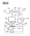
- FIG. 4 shows a portion of a gas field ion microscope that includes a flood gun 840 configured to deliver an electron beam 842 to surface 181 of sample 180 while a He ion beam 192 is incident on surface 181.
- the electron flux on surface 181 can, in general, be controlled so that surface charging effects are counterbalanced by electron beam 842 to the extent desired.
- FIG. 4 depicts ion beam 192 and electron beam 842 simultaneously impinging on surface 181 of sample 180
- flood gun 840 can be configured to deliver electron beam 842 to sample 180 to create a charge layer 846 in a sub-surface region of sample 180 ( FIG. 5 ).
- Layer 846 has an average depth m below surface 181, and layer 846 has a thickness r measured in a direction normal to surface 181.
- the depth m and thickness r, as well as the density of electrons in layer 846, can be controlled by the energy of the electrons in electron beam 842, the angle of incidence of the electrons in electron beam 842 with respect to surface 181, and the total dosage of electrons delivered to sample 180.
- the average energy of the electrons in electron beam 842 when incident on surface 181, is adjustable.
- the average energy of the electrons can be 500 eV or more (e.g., 1 keV or more, 2 keV or more), and/or 20 keV or less (e.g., 15 keV or less, 10 keV or less).
- the average energy of the electrons in electron beam 842 when incident on surface 181, can be from 500 eV to 20 keV (e.g., from 1 keV to 15 keV, from 2 keV to 10 keV).
- the angle of incidence ⁇ of the electrons in electron beam 842 with respect to surface 181 corresponds to the angle between a principal trajectory 850 of electron beam 842 and a normal 848 to surface 181.
- ⁇ is 0° or more (e.g., 10° or more, 20° or more), and/or 80° or less (e.g., 70° or less, 60° or less).
- ⁇ can be from 0° to 70° (e.g., from 0° to 10°, from 40° to 60°).
- the total current of electrons delivered to sample 180 is 10 pA or more (e.g., 100 pA or more, 1 nA or more, 10 nA or more), and/or 100 ⁇ A or less (e.g., 10 ⁇ A or less, 1 ⁇ A or less, 500 nA or less, 100 nA or less).
- the total current of electrons delivered to sample 180 can be from 10 pA to 1 ⁇ A (e.g., from 100 pA to 100 nA, from 1 nA to 10 nA).
- m is 10 nm or more (e.g., 25 nm or more, 50 nm or more, 75 nm or more, 100 nm or more), and/or 500 nm or less (e.g., 400 nm or less, 300 nm or less, 200 nm).
- m can be from 10 nm to 500 nm (e.g., from 25 nm to 500 nm, from 50 nm to 500 nm, from 75 nm to 400 nm, from 100 nm to 400 nm).
- multiple flood guns can be used.
- different flood guns can be used to expose different portions of surface 181 of sample 180 to electrons.
- each flood gun can be used to expose the same portion of surface 181 to electrons.
- different flood guns can be operated at different times. For example, one or more flood guns can be used to expose surface 181 to electrons before surface 181 is exposed to incident ions (e.g., to form a sub-surface charge layer), while one or more different flood guns can be used to expose surface 181 to electrons while surface 181 is also being exposed to incident ions.
- all the flood guns can be used to expose surface 181 to electrons before surface 181 is exposed to incident ions (e.g., to form a sub-surface charge layer), whereas in certain embodiments, all the flood guns can be used to expose surface 181 to electrons while surface 181 is also being exposed to incident ions. Other combinations may also be used.
- ion beam 192 can be formed of noble gas ions.
- ion beam 192 can be formed of one or more of helium ions, neon ions, krypton ions, and xenon ions.
- ion beam 192 can be formed of non-noble gas ions such as hydrogen ions.
- the implanted particle diffusion rate is temperature dependent, and increases with increasing temperature. Accordingly, in certain embodiments, the sample can be heated during exposure to ion beam 192 to increase the rate at which implanted particles leave the sample. When the sample is heated, implanted particles diffuse out of the sample faster, so that when ion beam 192 revisits a previously exposed portion of region 4000, the residual concentration of implanted particles therein is lower than if the sample had not been heated. As a result, sample damage and charging can be mitigated.
- each exposure spot on region 4000 corresponds to a particular portion of region 4000 that is exposed to ion beam 192. Particles which leave the sample in response to the incident ion beam are detected and generate an electronic signal that is correlated with the position of ion beam 192 relative to region 4000. A plurality of such electronic signals, together with their correlated positions, are used to form images of region 4000.
- each portion of region 4000 that is exposed to ion beam 192 corresponds to a single image pixel.
- region 4000 can be divided into an array of nxn regions, each corresponding to one of the image pixels.
- one or more portions (e.g., each portion) of region 4000 can correspond to multiple image pixels.
- successively exposed portions of region 4000 are spaced by a distance d s from one another along the x-axis.
- d s can represent the minimum spacing between successively exposed portions, and successively exposed portions can be spaced from one another by a distance d s or more along the x-axis.
- the spacing between successively exposed regions may or may not be equal between all pairs of regions.
- successively exposed portions can be variably spaced from one another along the x-axis. Variable spacing can be used, for example, where certain portions of the sample have relatively fine features that are best imaged at higher resolution so that smaller spacings between successively exposed portions are used. Conversely, portions that include relatively coarse (or no) features of interest can be imaged at lower resolution (larger spacings between successively exposed portions) to increase the speed of image acquisition.
- successive rows of exposed portions during implementation of the scanning protocol are spaced from one another by a distance e s in the y-direction.
- spacings between rows can vary, with e s representing a minimum spacing between pairs of exposed rows. Relatively short spacings can be used for imaging at higher resolution, while longer spacings can be used for lower resolution imaging and higher speed.
- d s and e s can have the same value so that exposed portions form a square pattern on region 4000, or different values so that a rectangular pattern is formed on region 4000.
- Scanning protocols can include moving ion beam 192 relative to region 4000 in the x-direction, in the y-direction, or in both the x- and y-directions between successively scanned portions.
- the x- and y-directions in general, may or may not be aligned with edges of region 4000 or of sample 180.
- patterns of exposure spots other than square and rectangular geometries can be used.
- circular (e.g., spiral) and/or elliptical patterns of exposure spots can be formed on region 4000.
- Ion beam 192 can be translated relative to region 4000 so that the ion beam exposes portions of region 4000 that form a series of concentric rings. The exposed portions can be spaced from one another by d s or more along the ring arcs, and concentric rings can be spaced along the radial direction by e s or more.
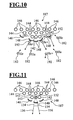
- FIG. 6 shows an example of a band scanning protocol applied to exposure of region 4000 to ion beam 192.
- Ion beam 192 is positioned initially in the upper left corner of region 4000 shown in FIG. 6 , and translated relative to region 4000 in the x-direction to form exposure line 5001 on region 4000.
- ion beam 192 is translated relative to region 4000, particles leave region 4000 in response to the incident ions. The particles are detected by one or more detectors and signals generated by the detectors are correlated with the positions of ion beam 192.
- ion beam 192 is re-positioned with respect to region 4000, and then scanned in the x-direction to form exposure line 5002.
- Repositioning of ion beam 192 includes translating ion beam 192 in the y-direction relative to region 4000 by an amount d t or more. A similar procedure is repeated to form exposure line 5003 on region 4000.
- ion beam 192 is re-positioned again with respect to region 4000, and then translated in the x-direction to form exposure line 5004.
- the process of re-positioning ion beam 192 and then translating the beam in the x-direction continues with formation of exposure lines 5005 and 5006.
- the pattern of exposing region 4000 along a series of exposure lines that are spaced by a distance d t from one another along the y-axis is repeated until all portions of region 4000 have been exposed.
- each exposure line includes a plurality of exposure spots.
- Ion beam 192 has an average spot size f s at the surface of region 4000, and the exposure spots in each exposure line are typically spaced from one another by a distance f s /2 or more in the x-direction. In general, however, any desired spacing of the exposure spots in the x-direction can be used.
- the distance d t between successively exposed lines on region 4000 can have the same value as d s discussed previously.
- the spacings between successive exposure lines can be constant or can vary, for example, to control the resolution at which different portions of region 4000 are imaged.
- a ratio d t /f s can be 2 or more (e.g., 3 or more, 4 or more, 5 or more, 10 or more, 15 or more, 20 or more, 25 or more, 30 or more) and/or 100 or less (e.g., 90 or less, 80 or less, 70 or less, 60 or less, 50 or less).
- Variations of the band scanning protocol can generally include any scanning protocol which prescribes forming exposure lines on region 4000, where doing so reduces sample damage and charging which would otherwise result from conventional scanning protocols such as raster scanning.
- all of the regions that correspond to the exposure lines are exposed the same number of times before any regions are exposed another time to ion beam 192.
- complete image frames are acquired before any portion of a new image frame is acquired.
- portions of region 4000 can be exposed multiple times to ion beam 192 while other portions are exposed to ion beam 192 a smaller number of times. This non-uniform exposure can be used, for example, to provide improved signal-to-noise ratios in images of certain portions of region 4000.
- images can be formed from interlaced image frames.
- ion beam 192 can be scanned relative to region 4000 to form a series of exposure lines on region 4000.
- the exposure lines can cover only a certain fraction (e.g., half) of region 4000, for example, and a first image frame can be formed based on particles leaving region 4000 in response to the incident ion beam.
- Ion beam 192 can then be scanned a second time relative to region 4000 to expose portions which were not exposed during the first scan.
- a second image frame can be formed based on particles leaving region 4000 in response to the incident ion beam.
- the first and second image frames can, for example, each include a series of alternating exposure lines on the surface of region 4000, so that the first and second image frames correspond to interlaced image frames.
- a complete image of region 4000 can be formed by combining the first and second image frames.
- different portions of the exposure lines can be formed on region 4000 at different times by scanning ion beam 192 relative to region 4000.
- ion beam 192 can be scanned along a first portion of each of the exposure lines shown in FIG. 6 in a first exposure step. Then, in a second exposure step, ion beam 192 can be scanned along the remaining portions of each of the exposure lines to complete exposure of region 4000.
- the exposure lines have a width gt measured in the y-direction.
- g t is 0.25 nm or more (e.g., 0.5 nm or more, 1 nm or more, 2 nm or more, 3 nm or more, 4 nm or more, 5 nm or more, 6 nm or more , 7 nm or more, 8 nm or more).
- a ratio d t /g t has a value of 2 or more (e. g., 3 or more, 4 or more, 5 or more, 6 or more, 7 or more, 10 or more, 15 or more, 20 or more, 30 or more, 40 or more, 50 or more).
- Table I Parameters of various scanning protocols are compared in Table I. To obtain the numbers shown in the table, a square exposure region with a side length of 100 nm was assumed. The square region was divided into an array of 1000 x 1000 pixels, each corresponding to an exposure spot. In addition, a minimum exposure time per pixel was established as 0.1 ⁇ s, corresponding to the maximum rate at which the ion beam could be translated relative to the sample.
- a region of a sample of interest is scanned line-by-line in a conventional raster pattern. That is, each successive row of the region is scanned from one end to the other, and the ion beam does not skip over rows during the scan.
- Table I for this scanning protocol, to avoid saturation of implanted He particles in the sample, the ion beam current must remain relatively low, which results in a relatively long acquisition time.
- each row of the region can be scanned multiple times before the ion beam moves to scan a successive row.
- the ion beam does not skip over rows during the scan.
- allowing the ion beam to revisit pixels in the same row multiple times before moving on to the next line permits higher ion beam currents to be used. As a result, the total acquisition time is reduced as shown in the second row of Table I.
- a frame averaging scanning protocol In a frame averaging scanning protocol, individual frames each corresponding to a pixel-averaged scan of the region - are obtained and combined to form the image. However, because the ion beam can re-scan each row of the region multiple times (e.g., once in each additional frame), the ion beam current can be further increased while avoiding saturation of implanted He particles in the sample. As shown in Table I, the frame averaging scanning protocol is effectively limited by the dwell time, which is in turn fixed by the maximum rate at which the ion beam can be translated relative to the region of interest.
- an image is acquired by scanning the region line-by-line, and the image can further be formed by integrating multiple frames.
- the difference between the frame averaging scanning protocol and the band scanning protocol is that in the band scanning protocol, successively scanned rows are separated by a distance d t measured along the y-direction. Due to the separation between successively scanned rows, interaction regions 3030 in portions of the sample that correspond to exposure spots in the scanned rows do not overlap too significantly with one another.
- the ratio of the exposure time per pixel to the time required for the ion beam to revisit the same pixel is roughly (d v /b v ).
- this ratio is roughly (d v /b v ) 2 , which has a significantly smaller value.
- Table I the band scanning protocol enables much higher ion beam currents to be used, and at the same time provides for shortened total acquisition times relative to the other scanning protocols.
- each image frame is subdivided into a series of square or rectangular sub-regions, and the ion beam visits a similar corresponding position in each sub-region before any sub-region is revisited. On subsequent visits from the ion beam, the relative position of the ion beam in each sub-region is shifted relative to the previous visit. Repeating this pattern exposes the entire region of interest.
- the checkerboard scanning protocol results in an even further reduction in spatial overlap between interaction regions 3030 that result from exposure of the sample to the ion beam.
- images of the sample can be formed by integrating multiple image frames.
- the ion beam current is limited to the same value as for the band scanning protocol due to the outgassing rate of implanted helium particles.
- the exposure time per pixel can increase due to the further decreased spatial overlap between interaction regions 3030, relative to the band scanning protocol. In fact, in the present calculations, the exposure time per pixel is constrained by the minimum dose of 600 particles per pixel.
- the exposure time per pixel could increase to 500 ⁇ s, which would help to reduce instrument noise that arises from rapid re-positioning of the ion beam.
- the increased exposure time per pixel could not be implemented in the other scanning protocols shown in Table I due to proximity of the interaction regions in each of the other protocols.
- a region 4000 of a sample 180 is to be exposed to ion beam 192 to obtain one or more images of the region.
- Region 4000 is typically a rectangular or square region with length R 1 and width R 2 .
- a side length S 1 of a square region 4050 is determined, where the square region 4050 corresponds to the smallest square region that fully encloses region 4000.
- determining the side length S 1 of square region 4050 for a rectangular or square region 4000 corresponds to determining a maximum dimension (e.g., R 1 or R 2 ) of region 4000.
- S 1 R 1.
- region 4000 may not be a square region, although in general, determining the side length of square region 4050 will still correspond to determining a maximum dimension of region 4000.
- Region 4000 has an area A.
- the next step in the procedure is to set the side length of square region 4050, S 1 , equal to the product F ⁇ A , where F is a numerical constant that is then easily determined. If region 4000 is a square region, then the value of F will be 1. However, if region 4000 is not square, then F can generally have values other than 1.
- region 4000 is divided into a series af M square portions, each of which has the same area and is to be separately exposed to ion beam 192.
- each of the M portions corresponds to a number of image pixels in images of region 4000.
- images of region 4000 include U total pixels, and each of the M portions corresponds to between 4 pixels and U/4 pixels of the image.
- Exposure of region 4000 to form a single image frame proceeds as follows. For each of the M portions of region 4000, a subset of the portion is continuously exposed to the ion beam for a time period t 1 . The subset of the portion corresponds to one or more pixels in images of the portion. Then, the ion beam is translated so that a subset of another portion is continuously exposed to the ion beam. Eventually, the ion beam returns to each of the M portions to expose a different subset of each portion (e.g., a subset of each portion which has not already been exposed to the ion beam). The exposing of subsets of portions, followed by translation of the ion beam to other portions, continues until all subsets of each of the portions have been exposed to the ion beam, thereby completing exposure of region 4000 and formation of a single image frame.
- the exposed subsets of each of the M portions correspond to equal numbers of image pixels. In certain embodiments, the exposed subsets correspond to different numbers of image pixels.
- the M portions can, in some embodiments, be determined according to an approximate interaction volume of incident ions with the material of region 4000. The interaction volume can be measured experimentally and used to determine the number (and therefore, the spacing) of portions M in region 4000. Alternatively, or in addition, the interaction volume of incident ions with the material of region 4000 can be estimated from a database such as a table of measured interaction volumes in particular materials. Once the interaction volume is estimated from such a database, the number and spacing of portions M in region 4000 can be determined.
- the time period between successive continuous exposures of one of the M portions to the ion beam is the same for that one portion, and the same for all M portions of region 4000. More generally, however, the time period between successive continuous exposures of one of the M portions to the ion beam can vary for a given portion, and can vary from portion to portion within region 4000.
- the time period t 2 is the shortest time period between successive exposures of any of the M portions to the ion beam.
- the values of t 1 and t 2 can vary widely according to different exposure protocols. In general, however, the time periods t 1 and t 2 are selected so that t 1 t 1 + t 2 ⁇ 1 2 ⁇ F ⁇ 1 M
- Equation (1) represents an upper limit on the value of the ratio t 1 t 1 + t 2 .
- the value of this ratio can be equal to or less than the value shown on the right side of Equation (1).
- the value of t 1 t 1 + t 2 is / 1 3 ⁇ F ⁇ / 1 M or less (e.g., / 1 4 ⁇ F ⁇ / 1 M or less, / 1 5 ⁇ F ⁇ / 1 M or less, / 1 10 ⁇ F ⁇ / 1 M or less, or even less).
- any of the scanning protocols disclosed herein can be implemented according to the relationship discussed above between the continuous exposure time t 1 of the M portions and the shortest time period t 2 between successive exposures of any of the M portions.
- both the checkerboard scanning protocol and the band scanning protocol, and variations thereof, can be implemented according to the relationship in Equation (1) to mitigate sample damage and charging.
- Each image pixel corresponds to a single exposure spot (e.g., where the ion beam exposes a spot in region 4000), and the exposure time for each spot is 1 ⁇ s. Therefore, without accounting for beam translation time and other factors, the total time required to expose all spots in region 4000 (e.g., all pixels in an image of region 4000) is 1 second.
- each of the M portions is exposed to the ion beam in the same manner for purposes of clarity.
- rows of exposure spots in region 4000 are exposed sequentially to the ion beam. For example, referring to FIG. 7A , rows are exposed in the order 1 ⁇ 2 ⁇ 3 ⁇ 4 ⁇ 5 ... -- 1000 to complete acquisition of an image of region 4000.
- the shortest time period between successive exposures of any one of the M portions to the ion beam, t 2 is the same for all portions.
- the ion beam exposes 100 spots in each of portions M2 through M10, and then returns to portion M1 to expose 100 spots in row 2.
- each of the rows of pixels (e.g., rows 1-100) in portions M1-M10 are exposed sequentially to the ion beam. Then, portions M11-M20 are skipped, and the rows of pixels (e.g., rows 201-300) in portions M21-M30 are exposed sequentially to the ion beam.
- a band scanning protocol such as the protocol shown schematically in FIG. 6
- single rows of spots within each of the M portions are exposed before additional rows of spots in any of the M portions are exposed.
- rows 1, 101, 201, 301, ... 901 are exposed, followed by rows 2, 102, 202, 302, ... 902, and so on.
- the shortest time between successive exposures of each of the portions is 9900 ⁇ s.
- t 2 corresponds to the time period between exposure of the last spot in row 1 of portion M1 and the first spot in row 2 of portion M1.
- This period includes 900 ⁇ s during which other spots in row 1 (e.g., in portions M2-M10) are exposed, and 9000 ⁇ s during which 1000 spots in each of rows 101, 201, 301, ... 901 are exposed.
- spots within each of the M portions are exposed before additional spots in any of the M portions are exposed.
- spots (1,1), (1,101), (1,201), ... (1,901), (101,1), (101,101), ... (901,901) are exposed-each of portions M1-M100 including exactly one of these spots) - and then the ion beam returns to portion M1 to expose (1,2), followed by (1,102) in portion M2, (1,202) in portion M3, and so on.
- the band scanning and checkerboard scanning protocols satisfy the relationship given by Equation (1), and are therefore effective at reducing sample damage and/or charging that arises from ion beam exposure.
- Gas assisted chemistry is commonly used during semiconductor fabrication to add material to and/or remove material from a given layer in a multi-layer semiconductor device.
- gas assisted chemistry can be used for semiconductor circuit editing - to repair damaged or incorrectly fabricated circuits formed in semiconductor articles.
- Gas assisted chemistry can also be used in photolithographic mask repair, where material can be added to or removed from masks to repair defects which result from use or incorrect fabrication.
- the process generally involves interacting electrons with an activating gas to form a reactive gas that can then participate in chemistry at the surface of a semiconductor article to add material to the surface, remove material from the surface, or both.
- the electrons are generated as secondary electrons resulting from the interaction of a Ga ion beam with the sample and/or the electrons are generated as secondary electrons resulting from the interaction of an electron beam (e.g., produced by a SEM) with the sample.
- an appropriate pumping system can be used to remove undesirable volatile products of the surface chemistry.
- activating gases that can be used to remove material from the surface include Cl 2 , O 2 , I 2 , XeF 2 , F 2 , CF 4 and H 2 O.
- a surface region formed of chrome, chrome oxide, chrome nitride and/or chrome oxynitride can be at least partially removed by interacting electrons with Cl 2 and/or O 2 , and allowing the resulting chemical species to etch the surface region.
- a surface region formed of a tantalum nitride can be at least partially removed by interacting electrons with XeF 2 , F 2 and/or CF 4 , and allowing the resulting chemical species to etch the surface region.
- a surface region formed of a carbon-containing material can be at least partially removed by interacting electrons with H 2 O and/or O 2 , and allowing the resulting chemical species to etch the surface region.
- An example of an activating gas that can be used to deposit a material on the surface is WF 6 (to deposit W, such as a W plug).
- An ion beam generated by the interaction of gas atoms with the gas field ion source (e.g., the He ion source) described herein can be used to perform gas assisted chemistry.
- the secondary electrons that leave the sample due to the interaction of the ion beam with the sample can be the electrons used to assist in the chemistry.
- Using such an ion beam can offer several advantages relative to using a Ga ion beam. As an example, undesirable ion implantation can be reduced (e.g., eliminated) using a He ion beam, whereas undesirable implantation of Ga is a common problem when a Ga ion beam is used.
- a gas field ion beam e.g., a He ion beam
- an incident electron beam e.g., an incident electron beam produced by a SEM
- This can, for example, reduce (e.g., eliminate) the undesirable interaction of ions with certain portions of a sample (e.g., such as can occur with a Ga ion beam where the beam profile has tails that extend to undesirable regions of the sample where Ga implantation can create problems with the performance of the semiconductor article).
- surface-adsorbed chemical agents interact with secondary electrons generated by the ion beam and undergo chemical reactions with the sample.
- the chemical reactions can lead to controlled structural modification of the sample.
- Consumed chemical agents on the sample surface can be replenished by exposing the sample to additional quantities of the agents (e.g., via a gas flow nozzle).
- the ion beam interrogates portions of the sample surface (e.g., ion beam spots) where the adsorbed chemical agents have already been depleted due to interactions with the ion beam positioned in a prior, adjacent location (e.g., beam spot).
- portions of the sample surface e.g., ion beam spots
- the ion beam is scanned according to the scanning protocols disclosed herein, sequential beam spots are spaced from one another by a larger amount than in conventional raster scanning protocols.
- the adsorbed chemical agents At each position of the ion beam on the surface of the sample, the adsorbed chemical agents have not yet interacted with secondary electrons produced by the ion beam or, alternatively, the adsorbed chemical agents have been replenished following a previous interaction with secondary electrons produced by the ion beam.
- the efficiency of ion beam-induced chemistry at the sample can be enhanced by scanning the sample surface with the ion beam according to the scanning protocols disclosed herein, so that the interval between successive exposures of any region of the sample is relatively long.
- This section discloses systems and methods for producing ion beams, and detecting particles that leave a sample of interest due to exposure of the sample to an ion beam.
- the systems and methods can be used to obtain one or more images of the sample.
- the gas ion beams that are used to interrogate samples are produced in multipurpose microscope systems.
- a gas field ion source is a device that includes an electrically conductive tip (typically having an apex with 10 or fewer atoms) that can be used to ionize neutral gas species to generate ions (e.g., in the form of an ion beam) by bringing the neutral gas species into the vicinity of the electrically conductive tip (e.g., within a distance of about four to five angstroms) while applying a high positive potential (e.g., one kV or more relative to the extractor (see discussion below)) to the apex of the electrically conductive tip.
- a high positive potential e.g., one kV or more relative to the extractor (see discussion below)
- FIG. 8 shows a schematic diagram of a gas field ion microscope system 100 that includes a gas source 110, a gas field ion source 120, ion optics 130, a sample manipulator 140, a front-side detector 150, a back-side detector 160, and an electronic control system 170 (e.g., an electronic processor, such as a computer) electrically connected to various components of system 100 via communication lines 172a-172f.
- a sample 180 is positioned in/on sample manipulator 140 between ion optics 130 and detectors 150, 160.
- an ion beam 192 is directed through ion optics 130 to a surface 181 of sample 180, and particles 194 resulting from the interaction of ion beam 192 with sample 180 are measured by detectors 150 and/or 160.
- gas field ion source 120 can be maintained at a pressure of approximately 10 -10 Torr.
- the background pressure rises to approximately 10 -5 Torr.
- Ion optics 130 are maintained at a background pressure of approximately 10 -8 Torr prior to the introduction of gas into gas field ion source 120.
- the background pressure in ion optics 130 typically increase to approximately 10 -7 Torr.
- Sample 180 is positioned within a chamber that is typically maintained at a background pressure of approximately 10 -6 Torr. This pressure does not vary significantly due to the presence or absence of gas in gas field ion source 120.
- gas source 110 is configured to supply one or more gases 182 to gas field ion source 120.
- gas source 110 can be configured to supply the gas(es) at a variety of purities, flow rates, pressures, and temperatures.
- at least one of the gases supplied by gas source 110 is a noble gas (helium (He), neon (Ne), argon (Ar), krypton (Kr), xenon (Xe)), and ions of the noble gas are desirably the primary constituent in ion beam 192.
- the current of ions in ion beam 192 increases monotonically as the pressure of the noble gas in system 100 increases.
- this relationship can be described by a power law where, for a certain range of noble gas pressures, the current increases generally in proportion to gas pressure.
- the pressure of the noble gas is typically 10 -2 Torr or less (e.g., 10 -3 Torr or less, 10 -4 Torr or less), and/or 10 -7 Torr or more (e.g., 10 -6 Torr or more, 10 -5 Torr or more) adjacent the tip apex (see discussion below).
- it is desirable to use relatively high purity gases e.g., to reduce the presence of undesirable chemical species in the system).
- the He when He is used, the He can be at least 99.99% pure (e.g., 99.995% pure, 99.999% pure, 99.9995% pure, 99.9999% pure).
- the purity of the gases is desirably high purity commercial grade.
- gas source 110 can supply one or more gases in addition to the noble gas(es).
- an example of such a gas is nitrogen.
- the additional gas(es) can be present at levels above the level of impurities in the noble gas(es), the additional gas(es) still constitute minority components of the overall gas mixture introduced by gas source 110.
- the overall gas mixture can include 20% or less (e.g., 15% or less, 12% or less) Ne, and/or 1% or more (e.g., 3% or more, 8% or more) Ne.
- the overall gas mixture can include from 5% to 15% (e.g., from 8% to 12%, from 9% to 11%) Ne.
- the overall gas mixture can include 1% or less (e.g., 0.5% or less, 0.1% or less) nitrogen, and/or 0.01% or more (e.g., 0.05% or more) nitrogen.
- the overall gas mixture can include from 0.01% to 1% (e.g., from 0.05% to 0.5%, from 0.08 to 0.12%) nitrogen.
- the additional gas(es) are mixed with the noble gas(es) before entering system 100 (e.g., via the use of a gas manifold that mixes the gases and then delivers the mixture into system 100 through a single inlet).
- the additional gas(es) are not mixed with the noble gas(es) before entering system 100 (e.g., a separate inlet is used for inputting each gas into system 100, but the separate inlets are sufficiently close that the gases become mixed before interacting with any of the elements in gas field ion source 120).
- Gas field ion source 120 is configured to receive the one or more gases 182 from gas source 110 and to produce gas ions from gas(es) 182.
- Gas field ion source 120 includes an electrically conductive tip 186 with a tip apex 187, an extractor 190 and optionally a suppressor 188.
- the distance from tip apex 187 to surface 181 of sample 180 is five cm or more (e.g., 10 cm or more, 15 cm or more, 20 cm or more, 25 cm or more), and/or 100 cm or less (e.g., 80 cm or less, 60 cm or less, 50 cm or less).
- the distance from tip apex 187 to surface 181 of sample 180 is from five cm to 100 cm (e.g., from 25 cm to 75 cm, from 40 cm to 60 cm, from 45 cm to 55 cm).
- Electrically conductive tip 186 can be formed of various materials.
- tip 186 is formed of a metal (e.g., tungsten (W), tantalum (Ta), iridium (Ir), rhenium (Rh), niobium (Nb), platinum (Pt), molybdenum (Mo)).
- electrically conductive tip 186 can be formed of an alloy.
- electrically conductive tip 186 can be formed of a different material (e.g., carbon (C)).
- tip 186 is biased positively (e.g., approximately 20 kV) with respect to extractor 190, extractor 190 is negatively or positively biased (e.g., from -20 kV to +50 kV) with respect to an external ground, and optional suppressor 188 is biased positively or negatively (e.g., from -5 kV to +5 kV) with respect to tip 186.
- tip 186 is formed of an electrically conductive material, the electric field of tip 186 at tip apex 187 points outward from the surface of tip apex 187. Due to the shape of tip 186, the electric field is strongest in the vicinity of tip apex 187.
- the strength of the electric field of tip 186 can be adjusted, for example, by changing the positive voltage applied to tip 186.
- un-ionized gas atoms 182 supplied by gas source 110 are ionized and become positively-charged ions in the vicinity of tip apex 187.
- the positively-charged ions are simultaneously repelled by positively charged tip 186 and attracted by negatively charged extractor 190 such that the positively-charged ions are directed from tip 186 into ion optics 130 as ion beam 192.
- Suppressor 188 assists in controlling the overall electric field between tip 186 and extractor 190 and, therefore, the trajectories of the positively-charged ions from tip 186 to ion optics 130.
- the overall electric field between tip 186 and extractor 190 can be adjusted to control the rate at which positively-charged ions are produced at tip apex 187, and the efficiency with which the positively-charged ions are transported from tip 186 to ion optics 130.
- He ions can be produced as follows.
- Gas field ion source 120 is configured so that the electric field of tip 186 in the vicinity of tip apex 187 exceeds the ionization field of the un-ionized He gas atoms 182, and tip 186 is maintained at a relatively low temperature.
- the He atoms can be polarized by the electric field of the tip, producing a weakly attractive force between He atoms 182 and tip apex 187.
- He atoms 182 may contact tip apex 187 and remain bound (e.g., physisorbed) thereto for some time.
- the electric field is high enough to ionize He atoms 182 adsorbed onto tip apex 187, generating positively charged He ions (e.g., in the form of an ion beam).
- FIG. 10 is a schematic representation of tip apex 187 (formed of W(111), see discussion below).
- Tip apex 187 includes layers of atoms arranged to form atomic shelves.
- a terminal atomic shelf is formed by atoms 142.
- a second atomic shelf is formed by atoms 144, and a third atomic shelf is formed by atoms 146.
- Neutral gas atoms 182 delivered by gas source 110 are present in the vicinity of tip apex 187.
- Atoms 182 become polarized due to the electric field of tip apex 187, and experience a relatively weak attractive force that causes atoms 182 to move towards tip apex 187, as indicated by the arrows on atoms 182.
- each atoms in the atomic shelves near tip apex 187 can have a corresponding ionization disk 148.
- An ionization disk 148 is a region of space in which a neutral He atom, venturing thereinto, has a high probability of undergoing ionization. Typically, ionization of a neutral He atom occurs via electron tunneling from the neutral He atom to a tip apex atom. Ionization disks 148 therefore represent spatial regions in which He ions are generated, and from which the He ions emerge.
- the sizes of the ionization disks 148 for particular tip apex atoms are dependent upon the shape of tip apex 187 and the electrical potential applied to tip apex 187.
- ionization of He atoms can occur in spatial regions adjacent to tip apex 187 where the local electric field exceeds the ionization potential of He atoms.
- many tip atoms will have ionization disks.
- the local electric field in the vicinity of tip apex 187 depends upon the shape of tip apex 187. For a relatively sharp tip apex, the local electric field in the vicinity of tip apex 187 will be relatively high. For a relatively blunt tip apex, the local electric field, even in the vicinity of tip apex 187, will be smaller.
- Ionization disks 148 corresponding to individual atoms of tip apex 187 are spatially separated from one another in FIG. 10 .
- ionization disks from more than one atom e.g., atoms 142
- the volume of space occupied by ionization disks 148 can be reduced, and the geometry depicted in FIG. 10 can be realized where a few tip apex atoms each have their own individual, spatially separated ionization disks.
- the electric field in the vicinity of tip apex 187 is typically controlled by adjusting the electrical potential applied to tip apex 187.
- tip apex 187 By further reducing the potential applied to tip apex 187, some of the ionization disks in FIG. 10 can be eliminated.
- tip apex 187 is not as sharp in the vicinity of second atomic shelf atoms 144, and by reducing the potential applied to tip apex 187, the electric field of tip apex 187 in the vicinity of atoms 144 can be reduced so that He atom ionization does not occur with high probability in these regions. As a result, ionization disks corresponding to atoms 144 are no longer present.
- tip apex 187 in the vicinity of terminal shelf atoms 142 can still be high enough to cause He atom ionization, and so ionization disks 148 corresponding to atoms 142 remain.
- ion source 120 can operate so that the only ionization disks present correspond to terminal shelf atoms 142, and the ionization disks corresponding to the terminal shelf atoms are spatially separated from one another.
- a He atom that is ionized in the vicinity of tip apex 187 is produced via ionization in the vicinity of a particular terminal shelf atom.
- Neutral He atoms 182 have a higher probability of undergoing ionization the longer they remain within ionization disks 148.
- the polarization of He atoms which is induced by the electric field of tip apex 187, and which causes polarized He atoms to move toward tip apex 187, further ensures that the polarized He atoms remain bound to tip apex 187, increasing the amount of time that the He atoms 182 remain within ionization disks 148, and increasing the probability of ionization of the polarized He atoms over time.
- Polarized He atoms can also move from one position to another along the surface of tip apex 187. Because the attractive force between a polarized He atom and tip apex 187 depends on the local strength of the electric field of tip apex 187 at the position of the polarized He atom, the motion of polarized He atoms tends to transport the atoms toward the end of tip apex 187 of tip 186 (e.g., toward terminal shelf 142) where the local electric field is highest.
- This transport mechanism of polarized He atoms in combination with control over the electrical potential applied to tip 186 (e.g., to ensure that discrete ionization disks corresponding to only terminal shelf atoms 142 are present), can be used to operate ion source 120 such that a He ion beam 192 is produced by gas field ionization source 120, where individual He ions in the ion beam are generated via the interaction of He gas with one of the terminal shelf atoms 142.
- Ion beam 192 therefore includes a plurality of He ions from each of the terminal shelf atoms 142, where each He ion can be attributed to ionization at one of the terminal shelf atoms 142.
- ionization disks 148 can be modified by changing the electrical potential applied to tip apex 187, and adjacent ionization disks 148 can be made to overlap with a suitably large applied potential, or maintained spatially distinct from one another by a suitably small applied potential.
- ionization disks 148 are spaced from tip atoms 142, 144, and 146 by a distance of approximately 0.4 nm.
- Individual ionization disks corresponding to tip atoms typically have a thickness of approximately 0.02 nm, measured in a direction along a line joining a given disk and its corresponding atom.
- Ionization disks 148 typically have a diameter, measured in a direction normal to the line joining a given disk and its corresponding atom, of approximately the diameter of the corresponding atom.
- FIG. 11 shows an operating configuration of tip apex 187 where the electrical potential applied to tip 186 produces three ionization disks 148, each of which corresponds to one of three terminal atomic shelf atoms 142.
- trajectories 156 are extrapolated backwards (e.g., along lines 154) to the position of the middle terminal shelf atom, they define a virtual source 152 for the middle terminal shelf atom.
- the diameter of virtual source 152 is typically smaller than the diameter of the middle terminal shelf atom, and may be much smaller than the diameter of the middle terminal shelf atom (e.g., by a factor of 2 or more, a factor of 3 or more, a factor of 5 or more, a factor of 10 or more). Similar considerations apply to the other terminal shelf atoms, and each terminal shelf atom has a corresponding virtual source size.
- the small virtual source size for terminal shelf atoms can provide a number of advantages.
- the small virtual source size of ion beam 192 and the relatively small thickness of the ionization disk 148 from which ions in ion beam 192 arise can assist in ensuring that ion beam 192 has a relatively high brightness and a relatively narrow ion energy distribution.
- the temperature of tip 186 is 5K or more (e.g., 10 K or more, 25K or more, 50K or more 75K or more), and/or 100K or less (e.g., 90K or less, 80K or less).
- the temperature of tip 186 can be from 5K to 100K (e.g., from 25K to 90K, from 50K to 90K, from 75K to 80K).
- the temperature of tip 186 can be attained by thermal coupling with a coolant, such as, for example, liquid helium or liquid nitrogen.
- a coolant such as, for example, liquid helium or liquid nitrogen.
- tip 186 can be thermally cooled using a cryogenic refrigerator.
- tip 186 It is also believed that, if the temperature of tip 186 is too high, polarized He atoms will have too much kinetic energy to remain bound to tip 186 for sufficiently long periods of time to ensure efficient ionization of He atoms in the vicinity of terminal shelf atoms 142. This can also result in disappearance of the emission pattern from individual terminal shelf atoms as observed using FIM and/or SFIM imaging techniques. As a result, to ensure that the He ionization process at each of the terminal shelf atoms 142 produces stable ion currents from each of the terminal shelf atoms 142, the temperature of tip 186 is carefully controlled to mitigate against both undesirable high- and low-temperature effects.
- ion optics 130 are configured to direct ion beam 192 onto surface 181 of sample 180.
- ion optics 130 can, for example, focus, collimate, deflect, accelerate, and/or decelerate ions in beam 192.
- Ion optics 130 can also allow only a portion of the ions in ion beam 192 to pass through ion optics 130.
- ion optics 130 include a variety of electrostatic and other ion optical elements that are configured as desired. By manipulating the electric field strengths of one or more components (e.g., electrostatic deflectors) in ion optics 130, He ion beam 192 can be scanned across surface 181 of sample 180.
- ion optics 130 can include two deflectors that deflect ion beam 192 in two orthogonal directions.
- the deflectors can have varying electric field strengths such that ion beam 192 is rastered across a region of surface 181.
- Detectors 150 and 160 are positioned and configured to each measure one or more different types of particles resulting from the interaction between He ion beam 192 and sample 180. As shown in FIG.
- detector 150 is positioned to detect particles 194 that originate primarily from surface 181 of sample 180
- detector 160 is positioned to detect particles 194 that emerge primarily from surface 183 of sample 180 (e.g., transmitted particles).
- any number and configuration of detectors can be used in the microscope systems disclosed herein.
- multiple detectors are used, and some of the multiple detectors are configured to measure different types of particles.
- the detectors are configured to provide different information about the same type of particle (e.g., energy of a particle, angular distribution of a given particle, total abundance of a given particle).
- combinations of such detector arrangements can be used.
- the information measured by the detectors is used to determine information about sample 180. Topically, this information is determined by obtaining one or more images of sample 180. By rastering ion beam 192 across surface 181, pixel-by-pixel information about sample 180 can be obtained in discrete steps.
- Detectors 150 and/or 160 can be configured to detect one or more different types of particles 194 at each pixel.
- a pixel is a square, although in some embodiments, pixels can have different shapes (e.g., rectangular).
- a pixel size, which corresponds to a length of a side of the pixel, can be, for example, from 100 pm to two ⁇ m (e.g., from one ⁇ m to one ⁇ m).
- the location of adjacent pixels can be determined to within at least 200 pm (e.g., to within at least 100 pm, to within at least 75 pm, to within at least 50 pm).
- the operator of the system can determine the location of the center of the beam spot to within at least 200 pm (e.g., to within at least 100 pm, to within at least 75 pm, to within at least 50 pm).
- the field of view (FOV) of sample 180 is 200 nm or more (e.g., 500 nm or more, 1 ⁇ m or more, 50 ⁇ m or more, 100 ⁇ m or more, 500 ⁇ m or more, 1 mm or more, 1.5 mm or more), and/or 25 mm or less (15 mm or less, 10 mm or less, five mm or less).
- the field of view refers to the area of a sample surface that is imaged by the ion microscope.
- microscope system 100 is typically controlled via electronic control system 170.
- electronic control system 170 can be configured to control the gas(es) supplied by gas source 110, the temperature of tip 186, the electrical potential of tip 186, the electrical potential of extractor 190, the electrical potential of suppressor 188, the settings of the components of ion optics 130, the position of sample manipulator 140, and/or the location and settings of detectors 150 and 160.
- one or more of these parameters may be manually controlled (e.g., via a user interface integral with electronic control system 170).
- electronic control system 170 can be used (e.g., via an electronic processor, such as a computer) to analyze the information collected by detectors 150 and 160 and to provide information about sample 180 (e.g., topography information, material constituent information, crystalline information, voltage contrast information, optical property information, magnetic information), which can optionally be in the form of an image, a graph, a table, a spreadsheet, or the like.
- electronic control system 170 includes a user interface that features a display or other kind of output device, an input device, and a storage medium.
- Electronic control system 170 can also be configured to scan ion beam 192 over a surface of sample 180 according to the scanning protocols disclosed herein.
- electronic control system 170 can be configured to permit manual (e.g., operator assisted) input of various scanning parameters such as the number and spacings of portions M in a scanning protocol.
- electronic control system 170 can be configured to determine various scanning parameters automatically (e.g., the number and spacings of portions M) based on input information (e.g., incident ion energy, sample material).
- electronic control system 170 can be configured to implement any of the scanning protocols disclosed herein in microscope system 100, with varying levels of automation from fully automatic operation to manual operation.
- FIG. 12 shows a schematic diagram of a He ion microscope system 200.
- Microscope system 200 includes a first vacuum housing 202 enclosing a He ion source and ion optics 130, and a second vacuum housing 204 enclosing sample 180 and detectors 150 and 160.
- Gas source 110 delivers He gas to microscope system 200 through a delivery tube 228.
- a flow regulator 230 controls the flow rate of He gas through delivery tube 228, and a temperature controller 232 controls the temperature of He gas in gas source 110.
- the He ion source includes a tip 186 affixed to a tip manipulator 208.
- the He ion source also includes an extractor 190 and a suppressor 188 that are configured to direct He ions from tip 186 into ion optics 130.
- Ion optics 130 include a first lens 216, alignment deflectors 220 and 222, an aperture 224, an astigmatism corrector 218, scanning deflectors 219 and 221, and a second lens 226.
- Aperture 224 is positioned in an aperture mount 234.
- Sample 180 is mounted in/on a sample manipulator 140 within second vacuum housing 204.
- Detectors 150 and 160 also positioned within second vacuum housing 204, are configured to detect particles 194 from sample 180.
- Gas source 110, tip manipulator 208, extractor 190, suppressor 188, first lens 216, alignment deflectors 220 and 222, aperture mount 234, astigmatism corrector 218, scanning deflectors 219 and 221, sample manipulator 140, and/or detectors 150 and/or 160 are typically controlled by electronic control system 170.
- electronic control system 170 also controls vacuum pumps 236 and 237, which are configured to provide reduced-pressure environments inside vacuum housings 202 and 204, and within ion optics 130.
- tip 186 can be formed of any appropriate electrically conductive material.
- tip 186 can be formed of a single crystal material, such as a single crystal metal.
- a particular single crystal orientation of the terminal shelf of atoms of tip apex 187 is aligned with a longitudinal axis of tip 186 to within 3° or less (e.g., within 2° or less, within 1° or less).
- apex 187 of tip 186 can terminate in an atomic shelf having a certain number of atoms (e.g., 20 atoms or less, 15 atoms or less, 10 atoms or less, nine atoms or less, six atoms or less, three atoms or less).
- apex 187 of tip 186 can be formed of W(111) and can have a terminal shelf with three atoms (a trimer).
- FIGS. 13 and 14 show schematic representations of enlarged top and side views, respectively, of the two atomic shelves of a W tip 186 that are nearest to the apex of tip.
- the terminal shelf which includes three W atoms 302 arranged in a trimer, corresponds to a (111) surface of W.
- this trimer surface is advantageous (in terms of its ease of formation, re-formation and stability) because the surface energy of the W(111) crystal face favorably supports a terminal shelf formed by three W atoms arranged in an equilateral triangle to form a trimer.
- the trimer atoms 302 are supported by a second shelf of W atoms 304.
- tip 186 can have a terminal shelf that includes fewer than three atoms or more than three atoms.
- a W(111) tip can have a terminal shelf that includes two atoms, or a terminal shelf that includes only one atom.
- a W(111) tip can have a terminal shelf that includes four or more atoms (e.g., five or more atoms, six or more atoms, seven or more atoms, eight or more atoms, nine or more atoms, ten or more atoms, more than ten atoms).
- tips that correspond to other W crystalline orientations can be used, and such tips can have terminal shelves that include one or more atoms (e.g., two or more atoms, three or more atoms, four or more atoms, five or more atoms, six or more atoms, seven or more atoms, eight or more atoms, nine or more atoms, ten or more atoms, more than ten atoms).
- tips formed from a material other than single crystal W can be used in the ion source (e.g., a single crystal of a metal, such as a single crystal of one of the metals noted above), and such tips can have terminal shelves that include one or more atoms (e.g., two or more atoms, three or more atoms, four or more atoms, five or more atoms, six or more atoms, seven or more atoms, eight or more atoms, nine or more atoms, ten or more atoms, more than ten atoms).
- atoms e.g., two or more atoms, three or more atoms, four or more atoms, five or more atoms, six or more atoms, seven or more atoms, eight or more atoms, nine or more atoms, ten or more atoms, more than ten atoms.
- tip apex 187 can have an impact on the quality of the ion beam, which can have an impact on the performance of microscope system 200.
- tip apex 187 when viewed from the side, can be symmetrically formed about its longitudinal axis, or it can be asymmetrically formed about its longitudinal axis. In certain embodiments, from one or more side views, tip apex 187 may be symmetrically formed about its longitudinal axis, and, from one or more different side views, tip apex 187 may be asymmetrically formed about its longitudinal axis.
- FIG. 15 is a flow chart for a process 400 of making a W(111) tip having a terminal atomic shelf that is a trimer.
- a single crystal W(111) precursor wire is attached to a support assembly.
- the precursor wire is etched in an electrochemical bath to shape the tip of the wire.
- the etched tip is examined to verify that the tip has suitable geometrical features. Determination of geometrical features typically includes obtaining profile images of the etched tip and calculating various geometrical parameters from data obtained from the profile images. The inspection can be performed using a SEM, for example.
- step 408 the terminal shelf of the apex of the tip of the etched wire is formed into a trimer.
- This process generally involves imaging the tip (e.g., using FIM or SFIM) and shaping the tip (e.g., using field evaporation).
- apex 187 of tip 186 is aligned within system 200.
- microscope system 200 is evacuated using one or more vacuum pumps, and then heat is applied to tip 187 to remove, for example, oxides, condensates, and/or any other impurities that may have adhered to the tip surface.
- tip 186 is heated to a temperature of 900 K or more (e.g., 1000 K or more, 1100 K or more) for a duration of 10 s or more (e.g., 30 s or more, 60 s or more). Heating may also assist in re-faceting tip 186, in the event that the tip shape is compromised by the presence of impurities.
- 900 K or more e.g., 1000 K or more, 1100 K or more
- Heating may also assist in re-faceting tip 186, in the event that the tip shape is compromised by the presence of impurities.
- microscope system 200 can be operated in He ion mode in step 412 of process 400.
- tip 186 can be periodically monitored by operating microscope system 200 in FIM or SFIM mode. If the trimer structure remains intact at tip apex 187, then tip 186 can continue to be used to provide ion beam 192 to microscope system 200. However, under certain circumstances, FIM or SFIM imaging of tip 186 may reveal that the trimer structure is no longer intact on tip apex 187. In this case, tip 186 can first be field evaporated to round the tip and remove the damaged trimer structure, and then re-sharpened in situ (e.g., without removing tip 186 from microscope system 200) using a process as described above.
- alignment of tip 186 in microscope system 200 includes aligning a longitudinal axis 207 of tip 186 with a longitudinal axis 132 of ion optics 130 so that the distance d between axes 207 and 132 at apex 187 of tip 186 is less than 2 mm (e.g., less than 1 mm, less than 500 ⁇ m, less than 200 ⁇ m). In some embodiments, the angle between axes 207 and 132 at apex 187 of tip 186 is 2° or less (e.g., 1° or less, 0.5° or less, 0.2° or less). Extractor 190 includes an opening 191. In general, the shape of extractor 190 and of opening 191 can be selected as desired.
- extractor 190 is positioned further in the +z direction than tip 186, as shown in FIG. 16 .
- extractor 190 is positioned further in the -z direction than tip 186.
- tip 186 protrudes through extractor 190 and extends further along the z-axis in the +z direction than extractor 190.
- extractor 190 is shown as having a particular configuration in FIG. 16 , more generally, extractor 190 can be of any desired design.
- opening 191 can have curved sides of any desired shape.
- Extractor 190 can generally be biased either positively or negatively with respect to tip 186.
- the electrical potential applied to extractor 190 is -10 kV or more (e.g., -5 kV or more, 0 kV or more), and/or 20 kV or less (e.g., 15 kV or less, 10 kV or less) with respect to tip 186.
- suppressor 188 can also be present in the vicinity of tip 186.
- Suppressor 188 can be used, for example, to alter the electric field distribution in the vicinity of tip 186 by adjusting the potential applied to suppressor 188.
- suppressor 188 can be used to control the trajectory of He ions produced at tip 186.
- suppressor 188 is positioned further along in the +z-direction than tip 186.
- tip 186 is positioned further along in the +z-direction than suppressor 188, so that tip 186 extends through suppressor 188 in the +z-direction.
- microscope system 200 can be configured so that after passing through extractor 190, the energy of the ions in ion beam 192 can be selected as desired.
- the average energy of the ions in ion beam 192 is 5 keV or more (e.g., 10 keV or more, 20 keV or more, 30 keV or more) and/or 100 keV or less (e.g., 90 keV or less, 80 keV less, 60 keV or less, 50kV or less, 40 kV or less, 30 kV or less) after passing through entry opening 133 to ion optics 130.
- the energy of the ions in ion beam 192 is from 5 keV to 100 keV (e.g., from 10 keV to 90 keV, from 20 keV to 80 keV).
- higher ion energies e.g., 50 keV to 100 keV may be used.
- the energy of the ions in ion beam 192 can be changed without changing the ion current. That is, the electrical potential applied to tip 186 can be adjusted to modify the average energy of ion beam 192 without substantially changing the ion beam current from ion beam 192.
- Ion optics 130 generally include one or more elements such as lenses, deflectors, and filters, that can be used to collimate, focus, deflect, and shape the ion beam emerging from ion source 120 prior to the beam impinging on a sample.
- Detectors 150 and 160 are depicted schematically in FIG. 12 , with detector 150 positioned to detect particles from surface 181 of sample 180 (the surface on which the ion beam impinges), and detector 160 positioned to detect particles from surface 183 of sample 180.
- a wide variety of different detectors can be employed in microscope system 200 to detect different particles, and a microscope system 200 can typically include any desired number of detectors.
- the configuration of the various detector(s) can be selected in accordance with particles to be measured and the measurement conditions.
- a spectrally resolved detector may be used. Such detectors are capable of detecting particles of different energy and/or wavelength, and resolving the particles based on the energy and/or wavelength of each detected particles.
- a spectrally resolved detector includes componentry capable of directing particles to different regions of the detector based on the energy and/or wavelength of the particle.
- FIG. 17 shows a schematic diagram of an ET detector 600 that includes a particle selector 601, a conversion material 602, a support 604, a photon detector 606, and voltage sources 607 and 608.
- voltage source 607 applies a voltage of relatively small magnitude (e.g., 500 V or less, such as from 100 V to 500 V) to particle selector 601 (formed of a conductive material), and voltage source 608 applies a voltage of relatively large magnitude (e.g., 5 kV or more, 10 kV or more) to conversion material 602.
- a voltage of relatively small magnitude e.g., 500 V or less, such as from 100 V to 500 V
- voltage source 608 applies a voltage of relatively large magnitude (e.g., 5 kV or more, 10 kV or more) to conversion material 602.
- the ET detector is used to measure electrons from sample 180 (e.g., secondary electrons)
- the sign of the voltage applied to particle selector 601 and conversion material 602 is positive with respect to sample 180.
- sample 180 can also be biased (with respect to the common external ground) to assist in delivering particles from sample 180 to detector 600.
- the ET detector when used to measure secondary electrons from sample 180, the sample can be negatively biased relative to the common external ground. Applying a negative potential bias to manipulator 140 may be particularly useful, for example, when detecting secondary electrons generated in a high aspect ratio (e.g., deep) hole or via in the sample.
- the negative potential bias relative to the common external ground can assist in accelerating electrons out of the hole or via and away from the sample, making detection of the electrons easier.
- many of the secondary electrons might instead re-enter the sample at points along the hole or via walls, never escaping the hole or via to be detected.
- Sample 180 can be positively biased, for example, when the ET detector is used to measure ions from the sample.
- the magnitude of the electrical potential applied to bias the sample can be 5 V or more (e.g., 10 V or more, 15 V or more, 20 V or more, 30 V or more, 50 V or more, 100 V or more).
- Charged particles 610 e.g., electrons or ions
- Charged particles 610 from sample 180 are attracted to particle selector 601, pass through particle selector 601, and are accelerated toward conversion material 602.
- Charged particles 610 then collide with conversion material 602, generating photons 612.
- Photons 612 pass through support 604 and are detected by photon detector 606.
- An ET detector can be located at any position relative to sample 180 to detect neutral or charged particles.
- an ET detector is positioned adjacent to second lens 226 of ion optics 130.
- an ET detector can also be positioned such that it is tilted downward slightly towards sample 180 (e.g., in a similar configuration as that depicted for detector 150 in FIG. 12 ).
- an ET detector can be positioned in the vicinity of surface 183 of sample 180. Such a configuration may be desirable, for example, when seeking to measure secondary electrons from sample 180 that emerge from surface 183 (e.g., after being transmitted through sample 180).
- the ET detector can have a configuration that is similar to the configuration of detector 160 in FIG. 12 .
- a microchannel plate detector can be used to amplify a flux of secondary electrons, neutral atoms, or ions from a sample.
- Microchannel plates are typically formed from materials such as fused silica, and generally include a large number of small diameter channels arranged in the form of an array. Particles enter individual channels and collide with channel walls, generating free electrons. Typically, multiple free electrons are generated on each collision of a particle (neutral atom, ion, or electron) with a channel wall. As a result, a cascaded electron signal corresponding to an amplification of the input particle signal exits the microchannel plate.
- Microchannel plate-based detectors (which can include one or more microchannel plates) can be configured to detect ions, secondary electrons, and/or neutral atoms from sample 180.
- Neutral particles and/or ions e.g., secondary ions and atoms, scattered ions and primary atoms
- Microchannel plate-based detectors configured to measure neutrals and/or ions from sample 180 are generally located at positions similar to the position of detector 150 depicted in FIGS. 8 and 12 .
- neutral particles and/or ions e.g., transmitted ions
- a microchannel plate-based detector can be located at positions similar to the position of detector 160 in FIGS. 8 and 12 .
- Secondary electrons can be detected either from surface 181 (the surface on which the ion beam impinges) and/or surface 183 of sample 180 (the surface on the opposite side from where the ion beam impinges), and microchannel plate-based detectors configured to detect secondary electrons from sample 180 are located at positions similar to detector 150 and/or detector 160 as depicted in FIGS. 10 and 14 .
- microchannel plates amplify an incoming particle signal and convert the incoming signal to an outgoing electron signal.
- microchannel plate-based detectors can also include a conversion material, a screen, and a photon detector (see discussion above).
- microchannel plates are affixed directly to elements of ion optics 130.
- FIG. 18 shows a cross-sectional view of a microchannel plate detector 620 mounted directly to an electrostatic lens 226.
- Lens 226 has a conical shape, with a flat lower surface 622.
- Detector 620 is mounted directly to surface 622.
- ions, secondary electrons, and/or neutral atoms from sample 180 can be detected by microchannel plate detector 620.
- Detector 620 registers a current that is proportional to the detected particle flux, which can be conveyed to electronic control system 170.
- a conversion plate can be used to detect ions (e.g., scattered ions, secondary ions) from a sample or neutral particles (e.g., primary neutral He atoms) from the sample.
- ions e.g., scattered ions, secondary ions
- neutral particles e.g., primary neutral He atoms
- a conversion plate can be formed from a thin foil material that, when struck by an incident ion or atom, has a high secondary electron yield.
- An example of such a material is platinum.
- the secondary electron yield produces an abundance of secondary electrons that are readily detected, for example, by an appropriate electron detector configured, for example, as detectors 150 and/or 160 ( FIGS. 8 and 12 ).
- Channeltron detectors can also be used to detect particles such as electrons, ions and neutral atoms leaving a sample.
- Channeltron detectors function by amplifying particle signals through multiple internal collisions in a manner similar to that described in connection with microchannel plate detectors.
- Measurement of relatively weak secondary electron, ion, or neutral atom fluxes from sample 180 is possible by measuring the amplified particle signals that are output by a channeltron detector (e.g., using electronic control system 170).
- a channeltron detector can be located in a position similar to that depicted for detector 150 and/or detector 160 in FIGS. 10 and 14 .
- a channeltron detector is located in a position similar to the position of detector 150 and/or the position of detector 160 as depicted in FIGS. 8 and 12 .
- Phosphor-based detectors which include a thin layer of a phosphor material deposited atop a transparent substrate, and a photon detector such as a CCD camera, a PMT, or one or more diodes, can be used to detect electrons, ions and/or neutral particles from a sample. Particles strike the phosphor layer, inducing emission of photons from the phosphor which are detected by the photon detector. Phosphor-based detectors can be arranged in positions similar to those of detector 150 and/or detector 160 as depicted in FIGS. 8 and 12 , depending upon the type of particle that is measured (see discussion above).
- Solid state detectors can be used to detect secondary electrons, ions, and/or neutral atoms from a sample.
- a solid state detector can be constructed from a sensor formed of a material such as silicon, or a doped silicon material. When incident particles strike the sensor, electron-hole pairs are created in the sensor material, producing a current that can be detected by electronic control system 170. The number of electron-hole pairs generated by an incident particle, and therefore the corresponding magnitude of the current produced, depends in part upon the particle's energy.
- a solid state detector can be particularly useful for energy measurements of particles, which can be especially advantageous when detecting high energy particles (e.g., scattered He ions and neutral He atoms) from sample 180.
- scintillator-based detectors include a scintillator material that generates photons in response to being struck by an incident particle (electron, ion, or neutral atom).
- Suitable scintillator materials include, for example, YAG and YAP.
- the photon yield in scintillator-based detectors depends on the energy of the incident particles.
- a scintillator detector can be particularly useful for energy measurements of particles, which can be especially advantageous when detecting high energy particles (e.g., scattered He ions and neutral He atoms) from sample 180.
- Electrostatic prism detectors in which an electric and/or magnetic field is used to deflect incident ions, where the amount of deflection depends on the energy of the ions, can be used to spatially separate ions with different energies.
- Magnetic prism detectors may also be used to spatially separate ions based on the energy of the ions. Any of the suitable detectors discussed above (e.g., microchannel plates, channeltrons, and others) can then be used to detect the deflected ions.
- Quadrupole detectors can also be used to analyze energies of ions from a sample.
- a radio-frequency (RF) field within the quadrupole ensures that ions having a chosen mass and energy propagate along a straight, undeflected trajectory within the quadrupole. Ions with a different mass and/or energy propagate along a curved trajectory within the quadrupole. From the deflected position of ions within the quadrupole analyzer, energies of the ions can be determined.
- RF radio-frequency
- ion energy can be determined by placing a positively biased particle selector (e.g., a screen or mesh of electrically conductive material, or a cylindrical metal tube or ring) along the flight path of the ions and in front of the detector.
- the magnitude of the electrical potential applied to particle selector 601 can initially be very high (e.g., a value certain to prevent ions from sample 180 from passing therethrough), and the magnitude of the electrical potential can be reduced while using an appropriate detector (see discussion above) to detect the ions.
- the current of ions that reach the detector as a function of the magnitude of the potential bias on the particle selector can be used to determine information about the energy of the ions.
- detectors and detection schemes can be implemented to measure energies of electrons (e.g., secondary electrons) from a sample.
- Prism detectors in which an electric and/or magnetic field is used to deflect incident electrons, and where the amount of deflection depends on the energy of the electrons, can be used to spatially separate electrons with different energies. Any of the suitable detectors discussed above can then be used to detect the deflected electrons.
- electron energies can be determined by placing a negatively biased particle selector (e.g., a screen or mesh of electrically conductive material, or a cylindrical metal tube or ring) along the flight path of the electrons and in front of the detector.
- the magnitude of the electrical potential of the particle selector can initially be very high (e.g., a value certain to prevent the electrons from sample 180 from passing therethrough), and the magnitude of the electrical potential can be reduced while using an appropriate detector (see discussion above) to detect the electrons.
- the electron current that reaches the detector as a function of the magnitude of the applied electrical potential on the particle selector can be used to determine information about the energies of the electrons.
- the detectors disclosed above can also be configured to measure lime-of-flight information for secondary electrons, ions, and neutral atoms.
- ion beam 192 is operated in pulsed mode.
- Ion beam 192 can be pulsed, for example, by rapidly changing the electrical potentials applied to one or more beam deflectors. By increasing these potentials, for example, ion beam 192 can be diverted from its usual path in ion optics 130 such that ion beam 192 is temporarily blocked by aperture 224. If the potentials of the deflectors are then returned to their normal values for a short time before being increased again, a pulse of He ions can be delivered to sample 180.
- detectors 150 and 160 can be synchronized to a clock signal from electronic control system 170 that is based upon the temporal variation in potentials applied to the deflectors.
- the time interval between the launch of a He ion pulse and the detection of particles from sample 180 can be accurately measured. From known information about the time of propagation of the He ion pulse within ion optics 130, the time-of-flight of the detected particles between sample 180 and detectors 150 and/or 160 can be determined.
- angle-dependent scattering information can be obtained using the detectors disclosed above.
- a detector is affixed to a mount (e.g., a swivel mount) that permits movement of the detector throughout a range of solid angles about sample 180.
- a mount e.g., a swivel mount
- abundance and/or energy measurements of particles are recorded.
- the detector is sequentially re-positioned at different solid angles and the measurements are repeated to determine the angular dependence of the measured quantities.
- a limiting aperture such as a pinhole can be placed in front of the detector in the path of the scattered particles to further restrict the range of angles over which measurement of particles from sample 180 occurs.
- a standard photon detector such as a PMT can be used. If the photon flux emanating from sample 180 is sufficiently large, less sensitive photon detectors such as diodes, diode arrays, and CCD cameras can be used.
- the photon detector can also include various optical elements that can be configured, for example, to isolate a particular optical signal of interest from among other optical signals.
- the photon detector can include optical elements such as filters to select particular wavelength bands in the photon signal emerging from sample 180, which can provide material constituent information about sample 180.
- the filters can, for example, block photons of undesired wavelengths (e.g., by absorbing photons of undesired wavelengths, by reflecting photons of undesired wavelengths, by diverting photons of undesired wavelengths).
- the optical elements can provide spectral resolution (e.g., to measure the spectrum of photons generated by sample 180) by dispersing different wavelengths spatially (e.g., diffractive elements such as one or more gratings, and/or refractive elements such as one or more prisms, and/or one or more spectrometer systems that provide wavelength-resolved detection of photons).
- the photon detector can include polarization manipulating elements such as waveplates and/or polarizers.
- polarization manipulating elements can be configured to permit photons having only a selected polarization state to reach the PMT, for example, allowing polarization-selective detection of the photon signal emerging from sample 180 (e.g., to assist in determining crystalline orientation information for sample 180).
- the photon detector can also include optical elements such as mirrors, lenses, beamsplitters, and other elements for re-directing and manipulating incident photons (e.g., to increase the solid angle of the photons that are detected).
- photon detectors can be positioned to detect photons at any desired angle and distance from sample 180.
- a photon detector can be positioned to detect photons emerging from surface 181 (the surface of sample 180 upon which ion beam 192 is incident), or from surface 183 (the surface of sample 180 opposite to the surface upon which ion beam 192 is incident).
- multiple photon detectors can be used and configured to detect photons from surfaces 181 (the surface on which the ion beam impinges), 183 (the surface on the opposite side from where the ion beam impinges) and/or other surfaces of sample 180.
- Ion beam 192 can have a relatively small spot size on surface 181 of sample 180.
- the spot size of ion beam 192 on surface 181 of sample 180 can have a dimension of 10 nm or less (e.g., nine nm or less, eight nm or less, seven nm or less, six nm or less, five nm or less, four nm or less, three nm or less, two nm or less, one nm or less).
- the spot size of ion beam 192 on surface 181 of sample 180 has a dimension of 0.05 nm or more (e.g., 0.1 nm or more, 0.2 nm or more, 0.25 nm or more, 0.5 nm or more, 0.75 nm or more, one nm or more, two nm or more, three nm or more).
- the spot size of ion beam 192 on surface 181 has a dimension of from 0.05 nm to 10 nm (e.g., from 0.1 nm to 10 nm, 0.2 nm to 10 nm, 0.25 nm to 3 nm, 0.25 nm to one nm, 0.1 nm to 0.5 nm, 0.1 nm to 0.2 nm).
- spot size is determined as follows with reference to FIGS. 19A-19C .
- An island 1700 formed of gold and having a dimension of from 50 nm to 2000 nm is disposed on a carbon surface 1710.
- the gold island is formed, for example, by vapor deposition of gold onto the carbon surface.
- Measurement samples that include gold islands deposited on carbon, suitable for the resolution measurements described herein, are available commercially from Structure Probe Inc. (West Chester, PA), for example.
- the ion microscope is operated such that it moves ion beam 192 linearly across a portion of the gold island, as well as the portions of the carbon surface on one side of the gold island (arrow 1730).
- the intensity of secondary electrons is measured as a function of the location of the ion beam ( FIG. 19C ).
- Asymptotic lines 1740 and 1750 are calculated (or drawn) corresponding to the average total abundance values for the carbon and gold, and vertical lines 1760 and 1770 are calculated (or drawn) corresponding to the locations where the total abundance is 25% and 75%, respectively, of the abundance difference between asymptotic lines 1740 and 1750.
- the spot size of ion microscope 200 is the distance between lines 1760 and 1770.
- the current of ion beam 192 at surface 181 of sample 180 is one nA or less (e.g., 100 pA or less, 50 pA or less), and/or 0.1 fA or more (e.g., one fA or more, 10 fA or more, 50 fA or more, 100 fA or more, one pA or more, 10 pA or more).
- the current of ion beam 192 at surface 181 of sample 180 is from 0.1 fA to one nA (e.g., from 10 fA to 100 pA, from 100 fA to 50 pA).
- one current can be used to prepare the gas field ion microscope for use (e.g., a current of 10 fA or more), and a different current can be used to image the sample (e.g., a current of less than one fA, such as 0.1 fA).
- ion beam 192 has an energy spread at surface 181 of sample 180 of five eV or less (e.g., four eV or less, three eV or less, two eV or less, one eV or less, 0.5 eV or less). In some embodiments, ion beam 192 has an energy spread at surface 181 of sample 180 of 0.1 eV or more (e.g., 0.2 eV or more, 0.3 eV or more, 0.4 eV or more). For example, ion beam 192 can have an energy spread at surface 181 of sample 180 of from 0.1 eV to five eV (e.g., from 0.1 eV to three eV, from 0.1 eV to one eV).
- Ion beam 192 can have a relatively high brightness at surface 181 of sample 180.
- ion beam 192 can have a brightness of 1x10 9 A/cm 2 sr (e.g., 1x10 10 A/cm 2 sr or more, 1x10 11 A/cm 2 sr or more) at surface 181 of sample 180.
- the brightness can be increased by increasing the gas pressure adjacent to tip 186 and/or decreasing the temperature of tip 186.
- the brightness of an ion beam is measured as follows.
- the FWHM of the distribution of ion trajectories in ion beam 192 - in a region of space between extractor 190 and first lens 216 where the net electric field is relatively small and the ion trajectories are nearly straight lines - is determined in both the x- and y-directions.
- a total of 100 ion trajectories that fall within the FWHM width in both the x- and y-directions are chosen at random from the distribution of ion trajectories in ion beam 192.
- Each of the 100 ion trajectories is nearly a straight line, and is projected back toward tip apex 187.
- the spatial extent of the trajectories at a particular point z t along the z-axis is assessed by constructing, in a plane Z t parallel to the x-y plane and passing through point z t , the smallest-diameter circle that encloses all of the points of intersection of the back-propagated trajectories with the plane Z t .
- the diameter of the smallest-diameter circle is d sm .
- d sm typically, for points z t closer to tip apex 187, d sm will be smaller and for points z t closer to sample 180, d sm will be larger.
- d sm will be a minimum value d 0 . That is, the spatial extent of the trajectories in a plane parallel to the x-y plane will be a minimum.
- the diameter d 0 of the minimum-diameter circle at point z 0 is referred to as the virtual source size of microscope system 200.
- Ion beam 192 can have a relatively high reduced brightness at surface 181 of sample 180.
- ion beam 192 can have a reduced brightness of 5x10 8 A/m 2 srV or more (e.g., 1x10 9 A/cm 2 srV or more, 1x10 10 A/cm 2 srV or more) at surface 181 of sample 180.
- the reduced brightness of an ion beam is the brightness of the ion beam divided by the average energy of the ions in the ion beam at the position where the beam current is measured
- Ion beam 192 can have a relatively low etendue at a distal end 193 of extractor 190.
- ion beam 192 can have an etendue of 5x10 -21 cm 2 sr or less (e.g., 1x10 -22 cm 2 sr or less, 1x10 -23 cm 2 sr or less, 1x10 -23 cm 2 sr or less, 1x10 -24 cm 2 sr or less) at distal end 193 of extractor 190.
- the etendue of an ion beam is calculated as the mathematical product of the reciprocal of the brightness and the beam current.
- Ion beam 192 can have a relatively low reduced etendue at a distal end 193 of extractor 190.
- ion beam 192 can have a reduced etendue of 1x10 -16 cm 2 sr or less (e.g., 1x10 -17 cm 2 sr or less, 1x10 -18 cm 2 sr or less, 1x10 -19 cm 2 sr or less) at distal end 193 of extractor 190.
- Reduced etendue of an ion beam is the mathematical product of the etendue of the ion beam and the ratio of the average energy-to-charge of ions in the ion beam at the position where the beam current is measured.
- Ion beam 192 can have a relatively low angular convergence with respect to surface 181 of sample 180.
- the convergence half angle of ion beam 192 can be 5 mrad or less (e.g., 1 mrad or less, 0.5 mrad or less, 0.1 mrad or less), and/or 0.05 mrad or more.
- the convergence half angle of an ion beam is determined as follows. A sample that includes a gold island atop a carbon substrate, as described above, is mounted in ion microscope 200 and translated in the z-direction so that the position of the focus of ion beam 192 lies, as nearly as possible, at the highest elevation point along a diameter of the gold island.
- Ion beam 192 is then translated linearly along the diameter of the gold island and the focused spot size, s f , of the ion beam is measured, as described above.
- the convergence half angle of ion microscope 200 is ⁇ /2.
- Ion microscope 200 can have a relatively good resolution.
- the resolution of ion microscope 200 can be 10 nm or less (e.g., nine nm or less, eight nm or less, seven nm or less, six nm or less, five nm or less, four nm or less, three nm or less, two nm or less, one nm or less).
- the resolution of ion microscope 200 can be 0.05 nm or more (e.g., 0.1 nm or more, 0.2 nm or more, 0.25 nm or more, 0.5 nm or more, 0.75 nm or more, one nm or more, two nm or more, three nm or more).
- the resolution of ion microscope 200 can be from 0.05 nm to 10 nm (e.g., from 0.1 nm to 10 nm, 0.2 nm to 10 nm, 0.25 nm to 3 nm, 0.25 nm to one nm, 0.1 nm to 0.5 nm, 0.1 nm to 0.2 nm).
- the resolution of an ion beam refers to the size of the smallest feature that can be reliably measured from images obtained using the ion microscope.
- a size of a feature is reliably measured if it can be determined to within an error of 10% or less of the actual size of the feature, and with a standard deviation in the measured size of less than 5% of the actual size of the feature, from ten images of the feature obtained under similar conditions.
- Ion microscope 200 can be used to take a good quality image in a relatively short period of time.
- ion microscope 200 can have a quality factor of 0.25 or more (e.g., 0.5 or more, 0.75 or more, one or more, 1.5 or more, two or more).
- the quality factor is determined as follows.
- the sample is imaged pixel-by-pixel by sub-dividing the surface of the sample into an x-y array of 512 pixels by 512 pixels.
- the dwell time per pixel is 100 ns during the measurement.
- the total abundance of secondary electrons from the sample is measured as a function of the position of the ion beam on the surface of the sample.
- an average pixel intensity G 1 is determined, along with a standard deviation SD 1 from the distribution of Si pixel intensities.
- an average pixel intensity G 2 is determined, along with a standard deviation SD 2 from the distribution of Cu pixel intensities.
- the quality factor is calculated according to the equation G 1 - G 2 S ⁇ D 1 ⁇ S ⁇ D 2
- Surface 181 of sample 180 can undergo relatively little damage when exposed to ion beam 192.
- surface 181 of sample 180 can have a value of 25 nm or less (e.g., 20 nm or less, 15 nm or less, 10 nm or less, five nm or less) according to the damage test.
- the damage test is performed as follows. An atomically flat silicon (99.99% purity) sample with a four square ⁇ m field of view is imaged for 120 seconds while rastering the ion beam across the surface of the sample pixel-by-pixel using an ion beam current at the sample of 10 pA and a spot size of the ion beam at the sample of 10 nm or less.
- the four square ⁇ m field of view is broken into a 512 pixel by 512 pixel array for rastering purposes.
- the value of the damage test corresponds to the maximum distance of etching into the imaged portion of the silicon sample resulting from performing the damage test.
- Ion microscope 200 can have a relatively large depth of focus.
- the depth of focus of ion microscope 200 can be five nm or more (e.g., 10 nm or more, 100nm or more, one ⁇ m or more), and/or 200 ⁇ m or less (e.g., 100 ⁇ m or less, 10 ⁇ m or less).
- the depth of focus of ion microscope 200 can be from 200 ⁇ m to five nm (e.g., from 500 ⁇ m to five nm, from one mm to five nm).
- the depth of focus of an ion beam is measured in the following manner.
- a sample that includes gold islands formed on a carbon substrate (as discussed previously in connection with measurement of the He ion beam spot size) is inserted into the He ion microscope, and a measurement of the He ion beam spot size is performed as discussed above.
- the location of the sample along the z-axis is iteratively adjusted so that the position of the sample that yields the smallest He ion beam spot size is determined. This position along the z-axis is denoted z f .
- the spot size of the He ion beam at z f is denoted ss f .
- the sample is then translated in increments along the -z direction relative to z f .
- a gas field ion microscope e.g., He ion microscope
- a gas field ion microscope can be used to distinguish elements in a sample having very close atomic numbers (Z values) using, for example, secondary electron yield, scattered ion abundance, and/or angle- and energy-resolved scattered ion detection.
- the gas field ion microscope can be used to distinguish elements having atomic numbers (Z values) that differ only by one.
- a gas field ion microscope e.g., He ion microscope
- a gas field ion microscope can be used to distinguish elements in a sample having a very close masses using, for example, secondary electron yield, scattered ion abundance, and/or angle- and energy-resolved scattered ion detection.
- the gas field ion microscope can be used to distinguish elements having masses that differ by one atomic mass unit or less (e.g., 0.9 atomic mass unit or less, 0.8 atomic mass unit or less, 0.7 atomic mass unit or less, 0.6 atomic mass unit or less, 0.5 atomic mass unit or less, 0.4 atomic mass unit or less, 0.3 atomic mass unit or less, 0.2 atomic mass unit or less, 0.1 atomic mass unit or less).
- a sample may have domains formed of materials (e.g., alloys) having different average masses.
- the gas field ion microscope can, for example, be used to distinguish domains of material having masses that differ only by one atomic mass unit or less (e.g., 0.9 atomic mass unit or less, 0.8 atomic mass unit or less, 0.7 atomic mass unit or less, 0.6 atomic mass unit or less, 0.5 atomic mass unit or less, 0.4 atomic mass unit or less, 0.3 atomic mass unit or less, 0.2 atomic mass unit or less, 0.1 atomic mass unit or less).
- one atomic mass unit or less e.g., 0.9 atomic mass unit or less, 0.8 atomic mass unit or less, 0.7 atomic mass unit or less, 0.6 atomic mass unit or less, 0.5 atomic mass unit or less, 0.4 atomic mass unit or less, 0.3 atomic mass unit or less, 0.2 atomic mass unit or less, 0.1 atomic mass unit or less.
- any of the analysis methods described above can be implemented in computer hardware or software, or a combination of both.
- the methods can be implemented in computer programs using standard programming techniques following the methods and figures described herein.
- Program code is applied to input data to perform the functions described herein and generate output information.
- the output information is applied to one or more output devices such as a display monitor.
- Each program may be implemented in a high level procedural or object oriented programming language to communicate with a computer system.
- the programs can be implemented in assembly or machine language, if desired. In any case, the language can be a compiled or interpreted language.
- the program can run on dedicated integrated circuits preprogrammed for that purpose.
- Each such computer program is preferably stored on a storage medium or device (e.g., ROM or magnetic diskette) readable by a general or special purpose programmable computer, for configuring and operating the computer when the storage media or device is read by the computer to perform the procedures described herein.
- the computer program can also reside in cache or main memory during program execution.
- the analysis methods can also be implemented as a computer-readable storage medium, configured with a computer program, where the storage medium so configured causes a computer to operate in a specific and predefined manner to perform the functions described herein.
- an ion beam can be used.
- an electron beam can be used.
- an electron beam can be created using a scanning electron microscope.
- the scanning protocols disclosed herein have similar advantages, including reducing sample damage and/or charging that arises from electron beam exposure.
- Electron beam sources and scanning electron microscope systems are disclosed, for example, in: U.S. Patent No. 7,186,976 entitled “SCANNING ELECTRON MICROSCOPE"; U.S. Patent No. 7,105,814 entitled “ELECTRON MICROSCOPY SYSTEM AND ELECTRON MICROSCOPY METHOD"; U.S. Patent No.
Landscapes
- Chemical & Material Sciences (AREA)
- Analytical Chemistry (AREA)
- Analysing Materials By The Use Of Radiation (AREA)
- Electron Sources, Ion Sources (AREA)
Claims (16)
- Procédé comprenant :la détermination d'une longueur de coté
 l'exposition de chacune des M parties de la région de l'échantillon à un faisceau de particules chargées, dans laquelle chacune des M parties est exposée en continu au faisceau de particules chargées pour une durée t1 , une durée la plus courte entre des expositions successives de chacune des M parties au faisceau de particules chargées est t2 , et les durées t1 et t2 sont choisies de telle sorte qu'un rapport

- Le procédé de la revendication 1, dans lequel le rapport


- Le procédé de la revendication 1, dans lequel l'échantillon et le faisceau de particules chargées sont placés à l'intérieur d'une chambre commune ayant une pression de gaz inférieure à 10-2 Torr, et dans laquelle une pluralité de particules quittant l'échantillon est détectée par un détecteur placé à l'intérieur de la chambre commune.
- Le procédé de la revendication 1, comprenant de plus la formation d'une image de la région basée sur une pluralité de particules quittant la région.
- Le procédé de la revendication 4, comprenant de plus la visualisation de l'image de l'échantillon sur une unité de visualisation électronique pour un opérateur du système.
- Le procédé de la revendication 1, dans lequel un courant de particules chargées du faisceau de particules chargées est de 10 pA ou plus.
- Le procédé de la revendication 1, dans lequel chacune des M parties de la région est exposée au faisceau de particules chargées pendant un temps d'exposition de 100 µs ou moins.
- Le procédé de la revendication 4, dans lequel un courant de particules chargées du faisceau de particules chargées est de 1 pA ou plus, chacune des M parties est exposée au faisceau de particules chargées pendant un temps d'exposition de 100 µs ou moins, et l'image est formée pendant un temps total d'acquisition de 100 secondes ou moins.
- Le procédé de la revendication 4, dans lequel la pluralité de particules comprend des électrons secondaires.
- Le procédé de la revendication 4, dans lequel la pluralité de particules comprend au moins un membre du groupe constitué d'ions diffusés et d'atomes neutres diffusés.
- Le procédé de la revendication 4, dans lequel chacune des M parties comprend de multiples pixels d'images.
- Le procédé de la revendication 1, comprenant de plus le chauffage de la région pendant l'exposition au faisceau de particules chargées.
- Le procédé de la revendication 1, dans lequel la détermination de la longueur de coté du plus petit carré comprend la détermination de la dimension maximum de la région.
- Le procédé de la revendication 1, comprenant de plus l'exposition en succession directe d'une première pluralité de M parties au faisceau de particules chargées, la première pluralité de parties formant une rangée dans une première direction, le faisceau de particules chargées ayant une dimension moyenne du spot de taille f sur une surface de l'échantillon, chaque partie de la première pluralité de parties étant espacée de ses parties voisines d'une distance d'au moins d dans la première direction, et un rapport d/f étant de 2 ou plus.
- Le procédé de la revendication 14, comprenant de plus l'exposition en succession directe d'une seconde pluralité de M parties au faisceau due particules chargées, la seconde pluralité de parties formant une rangée dans la première direction parallèle à la rangée formée par la première pluralité de parties, chaque partie de la seconde pluralité de parties étant espacée de ses parties voisines dans la seconde pluralité de parties d'une distance d'au moins d dans la première direction, et étant espacée de la première pluralité de parties d'une distance d'au moins e dans une seconde direction orthogonale à la première direction.
- Le procédé de la revendication 15, dans lequel e est plus grand que d.
Applications Claiming Priority (2)
| Application Number | Priority Date | Filing Date | Title |
|---|---|---|---|
| US1422907P | 2007-12-17 | 2007-12-17 | |
| PCT/EP2008/067419 WO2009077450A2 (fr) | 2007-12-17 | 2008-12-12 | Balayage de faisceaux de particules chargées |
Publications (2)
| Publication Number | Publication Date |
|---|---|
| EP2238606A2 EP2238606A2 (fr) | 2010-10-13 |
| EP2238606B1 true EP2238606B1 (fr) | 2011-08-24 |
Family
ID=40497572
Family Applications (1)
| Application Number | Title | Priority Date | Filing Date |
|---|---|---|---|
| EP08862809A Active EP2238606B1 (fr) | 2007-12-17 | 2008-12-12 | Balayage de faisceaux de particules chargées |
Country Status (5)
| Country | Link |
|---|---|
| US (1) | US8304750B2 (fr) |
| EP (1) | EP2238606B1 (fr) |
| JP (1) | JP5473004B2 (fr) |
| AT (1) | ATE521979T1 (fr) |
| WO (1) | WO2009077450A2 (fr) |
Families Citing this family (40)
| Publication number | Priority date | Publication date | Assignee | Title |
|---|---|---|---|---|
| EP3557956A1 (fr) | 2004-07-21 | 2019-10-23 | Mevion Medical Systems, Inc. | Générateur de forme d'onde de fréquence radio programmable pour un synchrocyclotron |
| CN101361156B (zh) | 2005-11-18 | 2012-12-12 | 梅维昂医疗系统股份有限公司 | 用于实施放射治疗的设备 |
| US8003964B2 (en) | 2007-10-11 | 2011-08-23 | Still River Systems Incorporated | Applying a particle beam to a patient |
| US8933650B2 (en) | 2007-11-30 | 2015-01-13 | Mevion Medical Systems, Inc. | Matching a resonant frequency of a resonant cavity to a frequency of an input voltage |
| US8581523B2 (en) | 2007-11-30 | 2013-11-12 | Mevion Medical Systems, Inc. | Interrupted particle source |
| US8907277B2 (en) * | 2008-03-07 | 2014-12-09 | Carl Zeiss Microscopy, Llc | Reducing particle implantation |
| EP2288904A2 (fr) * | 2008-06-20 | 2011-03-02 | Carl Zeiss NTS, LLC. | Procédés, systèmes et composants d'inspection d'échantillons |
| US8884224B2 (en) * | 2009-04-08 | 2014-11-11 | Hermes Microvision, Inc. | Charged particle beam imaging assembly and imaging method thereof |
| WO2011034985A1 (fr) | 2009-09-17 | 2011-03-24 | Sciaky, Inc. | Fabrication de couche de faisceau d'électron |
| JP2013506959A (ja) * | 2009-09-30 | 2013-02-28 | カール ツァイス エヌティーエス エルエルシー | 可変エネルギー荷電粒子システム |
| WO2011123195A1 (fr) | 2010-03-31 | 2011-10-06 | Sciaky, Inc. | Méthodologie de balayage, et appareil et système pour la fabrication de couches par faisceau d'électrons au moyen d'un système de commande en boucle fermée |
| US8847173B2 (en) * | 2010-08-06 | 2014-09-30 | Hitachi High-Technologies Corporation | Gas field ion source and method for using same, ion beam device, and emitter tip and method for manufacturing same |
| TWI447385B (zh) * | 2011-09-16 | 2014-08-01 | Inotera Memories Inc | 一種使用聚焦離子束系統進行晶片平面成像的方法 |
| US10254739B2 (en) | 2012-09-28 | 2019-04-09 | Mevion Medical Systems, Inc. | Coil positioning system |
| WO2014052721A1 (fr) | 2012-09-28 | 2014-04-03 | Mevion Medical Systems, Inc. | Système de commande pour un accélérateur de particules |
| JP6254600B2 (ja) | 2012-09-28 | 2017-12-27 | メビオン・メディカル・システムズ・インコーポレーテッド | 粒子加速器 |
| TW201424467A (zh) | 2012-09-28 | 2014-06-16 | Mevion Medical Systems Inc | 一粒子束之強度控制 |
| EP2900325B1 (fr) | 2012-09-28 | 2018-01-03 | Mevion Medical Systems, Inc. | Réglage de l'énergie d'un faisceau de particules |
| US9185789B2 (en) | 2012-09-28 | 2015-11-10 | Mevion Medical Systems, Inc. | Magnetic shims to alter magnetic fields |
| WO2014052716A2 (fr) | 2012-09-28 | 2014-04-03 | Mevion Medical Systems, Inc. | Régénérateur de champ magnétique |
| JP6121544B2 (ja) | 2012-09-28 | 2017-04-26 | メビオン・メディカル・システムズ・インコーポレーテッド | 粒子ビームの集束 |
| ES2739634T3 (es) | 2012-09-28 | 2020-02-03 | Mevion Medical Systems Inc | Control de terapia de partículas |
| SG11201509479WA (en) | 2013-05-30 | 2015-12-30 | Goldway Technology Ltd | Method of marking material and system therefore, and material marked according to same method |
| US8791656B1 (en) | 2013-05-31 | 2014-07-29 | Mevion Medical Systems, Inc. | Active return system |
| US9730308B2 (en) | 2013-06-12 | 2017-08-08 | Mevion Medical Systems, Inc. | Particle accelerator that produces charged particles having variable energies |
| US9530612B2 (en) | 2013-07-08 | 2016-12-27 | Carl Zeiss Microscopy, Llc | Charged particle beam system and method of operating a charged particle beam system |
| CN110237447B (zh) | 2013-09-27 | 2021-11-02 | 梅维昂医疗系统股份有限公司 | 粒子治疗系统 |
| WO2015051640A1 (fr) | 2013-10-11 | 2015-04-16 | Goldway Technology Limited | Procédé de marquage sur des pierres précieuses comprenant des pierres précieuses et des diamants, et marquages et pierres précieuses marquées selon un tel procédé |
| US10675487B2 (en) | 2013-12-20 | 2020-06-09 | Mevion Medical Systems, Inc. | Energy degrader enabling high-speed energy switching |
| US9962560B2 (en) | 2013-12-20 | 2018-05-08 | Mevion Medical Systems, Inc. | Collimator and energy degrader |
| US9661736B2 (en) | 2014-02-20 | 2017-05-23 | Mevion Medical Systems, Inc. | Scanning system for a particle therapy system |
| US9950194B2 (en) | 2014-09-09 | 2018-04-24 | Mevion Medical Systems, Inc. | Patient positioning system |
| US9619728B2 (en) * | 2015-05-31 | 2017-04-11 | Fei Company | Dynamic creation of backup fiducials |
| US10786689B2 (en) | 2015-11-10 | 2020-09-29 | Mevion Medical Systems, Inc. | Adaptive aperture |
| WO2018009779A1 (fr) | 2016-07-08 | 2018-01-11 | Mevion Medical Systems, Inc. | Planification de traitement |
| US11103730B2 (en) | 2017-02-23 | 2021-08-31 | Mevion Medical Systems, Inc. | Automated treatment in particle therapy |
| CN111093767B (zh) | 2017-06-30 | 2022-08-23 | 美国迈胜医疗系统有限公司 | 使用线性电动机而被控制的可配置准直仪 |
| JP7311620B2 (ja) | 2019-03-08 | 2023-07-19 | メビオン・メディカル・システムズ・インコーポレーテッド | 粒子線治療システムのためのコリメータおよびエネルギーデグレーダ |
| DE102020103339A1 (de) | 2020-02-10 | 2021-08-12 | Carl Zeiss Microscopy Gmbh | Verfahren zum Betrieb eines Teilchenstrahlgeräts, Computerprogrammprodukt und Teilchenstrahlgerät zur Durchführung des Verfahrens |
| US11804361B2 (en) * | 2021-05-18 | 2023-10-31 | Nuflare Technology, Inc. | Charged particle beam writing method, charged particle beam writing apparatus, and computer-readable recording medium |
Family Cites Families (16)
| Publication number | Priority date | Publication date | Assignee | Title |
|---|---|---|---|---|
| JPH0638329B2 (ja) * | 1986-12-29 | 1994-05-18 | セイコー電子工業株式会社 | 集束イオンビーム走査方法 |
| JPH0638329A (ja) | 1992-07-17 | 1994-02-10 | Totoku Electric Co Ltd | 絶縁被膜剥離装置および型巻線の製造方法 |
| JP4054445B2 (ja) * | 1998-06-30 | 2008-02-27 | 株式会社東芝 | 荷電ビーム描画方法 |
| US6614026B1 (en) | 1999-04-15 | 2003-09-02 | Applied Materials, Inc. | Charged particle beam column |
| JP4053723B2 (ja) * | 2000-09-27 | 2008-02-27 | 株式会社東芝 | 露光用マスクの製造方法 |
| WO2002037526A1 (fr) * | 2000-11-02 | 2002-05-10 | Ebara Corporation | Appareil a faisceau electronique et procede de fabrication d'un dispositif a semi-conducteur comprenant ledit appareil |
| GB2374723B (en) * | 2001-04-20 | 2005-04-20 | Leo Electron Microscopy Ltd | Scanning electron microscope |
| JP2003045780A (ja) * | 2001-07-30 | 2003-02-14 | Nec Corp | マスク描画データの作成方法 |
| DE10233002B4 (de) | 2002-07-19 | 2006-05-04 | Leo Elektronenmikroskopie Gmbh | Objektivlinse für ein Elektronenmikroskopiesystem und Elektronenmikroskopiesystem |
| DE10236738B9 (de) | 2002-08-09 | 2010-07-15 | Carl Zeiss Nts Gmbh | Elektronenmikroskopiesystem und Elektronenmikroskopieverfahren |
| DE10331137B4 (de) | 2003-07-09 | 2008-04-30 | Carl Zeiss Nts Gmbh | Detektorsystem für ein Rasterelektronenmikroskop und Rasterelektronenmikroskop mit einem entsprechenden Detektorsystem |
| US7557359B2 (en) | 2003-10-16 | 2009-07-07 | Alis Corporation | Ion sources, systems and methods |
| US7511279B2 (en) * | 2003-10-16 | 2009-03-31 | Alis Corporation | Ion sources, systems and methods |
| US7259373B2 (en) | 2005-07-08 | 2007-08-21 | Nexgensemi Holdings Corporation | Apparatus and method for controlled particle beam manufacturing |
| JP4748714B2 (ja) * | 2005-10-28 | 2011-08-17 | エスアイアイ・ナノテクノロジー株式会社 | 荷電粒子ビーム走査照射方法、荷電粒子ビーム装置、試料観察方法、及び、試料加工方法 |
| US8907277B2 (en) * | 2008-03-07 | 2014-12-09 | Carl Zeiss Microscopy, Llc | Reducing particle implantation |
-
2008
- 2008-12-12 AT AT08862809T patent/ATE521979T1/de not_active IP Right Cessation
- 2008-12-12 JP JP2010538606A patent/JP5473004B2/ja active Active
- 2008-12-12 US US12/744,152 patent/US8304750B2/en active Active
- 2008-12-12 EP EP08862809A patent/EP2238606B1/fr active Active
- 2008-12-12 WO PCT/EP2008/067419 patent/WO2009077450A2/fr active Application Filing
Also Published As
| Publication number | Publication date |
|---|---|
| US8304750B2 (en) | 2012-11-06 |
| JP5473004B2 (ja) | 2014-04-16 |
| WO2009077450A3 (fr) | 2009-12-03 |
| US20100294930A1 (en) | 2010-11-25 |
| EP2238606A2 (fr) | 2010-10-13 |
| WO2009077450A2 (fr) | 2009-06-25 |
| ATE521979T1 (de) | 2011-09-15 |
| JP2011507202A (ja) | 2011-03-03 |
Similar Documents
| Publication | Publication Date | Title |
|---|---|---|
| EP2238606B1 (fr) | Balayage de faisceaux de particules chargées | |
| JP5643262B2 (ja) | イオン源、システム及び方法 | |
| US7804068B2 (en) | Determining dopant information | |
| US7557359B2 (en) | Ion sources, systems and methods | |
| US7554096B2 (en) | Ion sources, systems and methods | |
| US20070158555A1 (en) | Ion sources, systems and methods | |
| US20070158556A1 (en) | Ion sources, systems and methods | |
| US20070158557A1 (en) | Ion sources, systems and methods |
Legal Events
| Date | Code | Title | Description |
|---|---|---|---|
| PUAI | Public reference made under article 153(3) epc to a published international application that has entered the european phase |
Free format text: ORIGINAL CODE: 0009012 |
|
| 17P | Request for examination filed |
Effective date: 20100716 |
|
| AK | Designated contracting states |
Kind code of ref document: A2 Designated state(s): AT BE BG CH CY CZ DE DK EE ES FI FR GB GR HR HU IE IS IT LI LT LU LV MC MT NL NO PL PT RO SE SI SK TR |
|
| AX | Request for extension of the european patent |
Extension state: AL BA MK RS |
|
| GRAP | Despatch of communication of intention to grant a patent |
Free format text: ORIGINAL CODE: EPIDOSNIGR1 |
|
| DAX | Request for extension of the european patent (deleted) | ||
| GRAS | Grant fee paid |
Free format text: ORIGINAL CODE: EPIDOSNIGR3 |
|
| GRAA | (expected) grant |
Free format text: ORIGINAL CODE: 0009210 |
|
| AK | Designated contracting states |
Kind code of ref document: B1 Designated state(s): AT BE BG CH CY CZ DE DK EE ES FI FR GB GR HR HU IE IS IT LI LT LU LV MC MT NL NO PL PT RO SE SI SK TR |
|
| REG | Reference to a national code |
Ref country code: GB Ref legal event code: FG4D |
|
| REG | Reference to a national code |
Ref country code: CH Ref legal event code: EP |
|
| REG | Reference to a national code |
Ref country code: IE Ref legal event code: FG4D |
|
| REG | Reference to a national code |
Ref country code: DE Ref legal event code: R096 Ref document number: 602008009186 Country of ref document: DE Effective date: 20111103 |
|
| REG | Reference to a national code |
Ref country code: NL Ref legal event code: T3 |
|
| LTIE | Lt: invalidation of european patent or patent extension |
Effective date: 20110824 |
|
| PG25 | Lapsed in a contracting state [announced via postgrant information from national office to epo] |
Ref country code: SE Free format text: LAPSE BECAUSE OF FAILURE TO SUBMIT A TRANSLATION OF THE DESCRIPTION OR TO PAY THE FEE WITHIN THE PRESCRIBED TIME-LIMIT Effective date: 20110824 Ref country code: HR Free format text: LAPSE BECAUSE OF FAILURE TO SUBMIT A TRANSLATION OF THE DESCRIPTION OR TO PAY THE FEE WITHIN THE PRESCRIBED TIME-LIMIT Effective date: 20110824 Ref country code: IS Free format text: LAPSE BECAUSE OF FAILURE TO SUBMIT A TRANSLATION OF THE DESCRIPTION OR TO PAY THE FEE WITHIN THE PRESCRIBED TIME-LIMIT Effective date: 20111224 Ref country code: FI Free format text: LAPSE BECAUSE OF FAILURE TO SUBMIT A TRANSLATION OF THE DESCRIPTION OR TO PAY THE FEE WITHIN THE PRESCRIBED TIME-LIMIT Effective date: 20110824 Ref country code: NO Free format text: LAPSE BECAUSE OF FAILURE TO SUBMIT A TRANSLATION OF THE DESCRIPTION OR TO PAY THE FEE WITHIN THE PRESCRIBED TIME-LIMIT Effective date: 20111124 Ref country code: LT Free format text: LAPSE BECAUSE OF FAILURE TO SUBMIT A TRANSLATION OF THE DESCRIPTION OR TO PAY THE FEE WITHIN THE PRESCRIBED TIME-LIMIT Effective date: 20110824 Ref country code: PT Free format text: LAPSE BECAUSE OF FAILURE TO SUBMIT A TRANSLATION OF THE DESCRIPTION OR TO PAY THE FEE WITHIN THE PRESCRIBED TIME-LIMIT Effective date: 20111226 |
|
| REG | Reference to a national code |
Ref country code: AT Ref legal event code: MK05 Ref document number: 521979 Country of ref document: AT Kind code of ref document: T Effective date: 20110824 |
|
| PG25 | Lapsed in a contracting state [announced via postgrant information from national office to epo] |
Ref country code: SI Free format text: LAPSE BECAUSE OF FAILURE TO SUBMIT A TRANSLATION OF THE DESCRIPTION OR TO PAY THE FEE WITHIN THE PRESCRIBED TIME-LIMIT Effective date: 20110824 Ref country code: PL Free format text: LAPSE BECAUSE OF FAILURE TO SUBMIT A TRANSLATION OF THE DESCRIPTION OR TO PAY THE FEE WITHIN THE PRESCRIBED TIME-LIMIT Effective date: 20110824 Ref country code: AT Free format text: LAPSE BECAUSE OF FAILURE TO SUBMIT A TRANSLATION OF THE DESCRIPTION OR TO PAY THE FEE WITHIN THE PRESCRIBED TIME-LIMIT Effective date: 20110824 Ref country code: LV Free format text: LAPSE BECAUSE OF FAILURE TO SUBMIT A TRANSLATION OF THE DESCRIPTION OR TO PAY THE FEE WITHIN THE PRESCRIBED TIME-LIMIT Effective date: 20110824 Ref country code: CY Free format text: LAPSE BECAUSE OF FAILURE TO SUBMIT A TRANSLATION OF THE DESCRIPTION OR TO PAY THE FEE WITHIN THE PRESCRIBED TIME-LIMIT Effective date: 20110824 Ref country code: GR Free format text: LAPSE BECAUSE OF FAILURE TO SUBMIT A TRANSLATION OF THE DESCRIPTION OR TO PAY THE FEE WITHIN THE PRESCRIBED TIME-LIMIT Effective date: 20111125 |
|
| PG25 | Lapsed in a contracting state [announced via postgrant information from national office to epo] |
Ref country code: BE Free format text: LAPSE BECAUSE OF FAILURE TO SUBMIT A TRANSLATION OF THE DESCRIPTION OR TO PAY THE FEE WITHIN THE PRESCRIBED TIME-LIMIT Effective date: 20110824 |
|
| PG25 | Lapsed in a contracting state [announced via postgrant information from national office to epo] |
Ref country code: SK Free format text: LAPSE BECAUSE OF FAILURE TO SUBMIT A TRANSLATION OF THE DESCRIPTION OR TO PAY THE FEE WITHIN THE PRESCRIBED TIME-LIMIT Effective date: 20110824 |
|
| PG25 | Lapsed in a contracting state [announced via postgrant information from national office to epo] |
Ref country code: IT Free format text: LAPSE BECAUSE OF FAILURE TO SUBMIT A TRANSLATION OF THE DESCRIPTION OR TO PAY THE FEE WITHIN THE PRESCRIBED TIME-LIMIT Effective date: 20110824 Ref country code: EE Free format text: LAPSE BECAUSE OF FAILURE TO SUBMIT A TRANSLATION OF THE DESCRIPTION OR TO PAY THE FEE WITHIN THE PRESCRIBED TIME-LIMIT Effective date: 20110824 Ref country code: RO Free format text: LAPSE BECAUSE OF FAILURE TO SUBMIT A TRANSLATION OF THE DESCRIPTION OR TO PAY THE FEE WITHIN THE PRESCRIBED TIME-LIMIT Effective date: 20110824 |
|
| PG25 | Lapsed in a contracting state [announced via postgrant information from national office to epo] |
Ref country code: DK Free format text: LAPSE BECAUSE OF FAILURE TO SUBMIT A TRANSLATION OF THE DESCRIPTION OR TO PAY THE FEE WITHIN THE PRESCRIBED TIME-LIMIT Effective date: 20110824 |
|
| PLBE | No opposition filed within time limit |
Free format text: ORIGINAL CODE: 0009261 |
|
| STAA | Information on the status of an ep patent application or granted ep patent |
Free format text: STATUS: NO OPPOSITION FILED WITHIN TIME LIMIT |
|
| PG25 | Lapsed in a contracting state [announced via postgrant information from national office to epo] |
Ref country code: MC Free format text: LAPSE BECAUSE OF NON-PAYMENT OF DUE FEES Effective date: 20111231 |
|
| 26N | No opposition filed |
Effective date: 20120525 |
|
| REG | Reference to a national code |
Ref country code: DE Ref legal event code: R097 Ref document number: 602008009186 Country of ref document: DE Effective date: 20120525 |
|
| REG | Reference to a national code |
Ref country code: IE Ref legal event code: MM4A |
|
| PG25 | Lapsed in a contracting state [announced via postgrant information from national office to epo] |
Ref country code: IE Free format text: LAPSE BECAUSE OF NON-PAYMENT OF DUE FEES Effective date: 20111212 |
|
| PG25 | Lapsed in a contracting state [announced via postgrant information from national office to epo] |
Ref country code: MT Free format text: LAPSE BECAUSE OF FAILURE TO SUBMIT A TRANSLATION OF THE DESCRIPTION OR TO PAY THE FEE WITHIN THE PRESCRIBED TIME-LIMIT Effective date: 20110824 |
|
| REG | Reference to a national code |
Ref country code: DE Ref legal event code: R081 Ref document number: 602008009186 Country of ref document: DE Owner name: CARL ZEISS MICROSCOPY GMBH, DE Free format text: FORMER OWNER: CARL ZEISS NTS GMBH, 73447 OBERKOCHEN, DE Effective date: 20130319 |
|
| PG25 | Lapsed in a contracting state [announced via postgrant information from national office to epo] |
Ref country code: LU Free format text: LAPSE BECAUSE OF NON-PAYMENT OF DUE FEES Effective date: 20111212 |
|
| PG25 | Lapsed in a contracting state [announced via postgrant information from national office to epo] |
Ref country code: BG Free format text: LAPSE BECAUSE OF FAILURE TO SUBMIT A TRANSLATION OF THE DESCRIPTION OR TO PAY THE FEE WITHIN THE PRESCRIBED TIME-LIMIT Effective date: 20111124 |
|
| REG | Reference to a national code |
Ref country code: CH Ref legal event code: PL |
|
| PG25 | Lapsed in a contracting state [announced via postgrant information from national office to epo] |
Ref country code: TR Free format text: LAPSE BECAUSE OF FAILURE TO SUBMIT A TRANSLATION OF THE DESCRIPTION OR TO PAY THE FEE WITHIN THE PRESCRIBED TIME-LIMIT Effective date: 20110824 |
|
| PG25 | Lapsed in a contracting state [announced via postgrant information from national office to epo] |
Ref country code: HU Free format text: LAPSE BECAUSE OF FAILURE TO SUBMIT A TRANSLATION OF THE DESCRIPTION OR TO PAY THE FEE WITHIN THE PRESCRIBED TIME-LIMIT Effective date: 20110824 Ref country code: CH Free format text: LAPSE BECAUSE OF NON-PAYMENT OF DUE FEES Effective date: 20121231 Ref country code: LI Free format text: LAPSE BECAUSE OF NON-PAYMENT OF DUE FEES Effective date: 20121231 Ref country code: ES Free format text: LAPSE BECAUSE OF FAILURE TO SUBMIT A TRANSLATION OF THE DESCRIPTION OR TO PAY THE FEE WITHIN THE PRESCRIBED TIME-LIMIT Effective date: 20111205 |
|
| PGFP | Annual fee paid to national office [announced via postgrant information from national office to epo] |
Ref country code: GB Payment date: 20141219 Year of fee payment: 7 |
|
| PGFP | Annual fee paid to national office [announced via postgrant information from national office to epo] |
Ref country code: FR Payment date: 20141219 Year of fee payment: 7 |
|
| GBPC | Gb: european patent ceased through non-payment of renewal fee |
Effective date: 20151212 |
|
| REG | Reference to a national code |
Ref country code: FR Ref legal event code: ST Effective date: 20160831 |
|
| PG25 | Lapsed in a contracting state [announced via postgrant information from national office to epo] |
Ref country code: GB Free format text: LAPSE BECAUSE OF NON-PAYMENT OF DUE FEES Effective date: 20151212 |
|
| PG25 | Lapsed in a contracting state [announced via postgrant information from national office to epo] |
Ref country code: FR Free format text: LAPSE BECAUSE OF NON-PAYMENT OF DUE FEES Effective date: 20151231 |
|
| PGFP | Annual fee paid to national office [announced via postgrant information from national office to epo] |
Ref country code: NL Payment date: 20211221 Year of fee payment: 14 |
|
| REG | Reference to a national code |
Ref country code: NL Ref legal event code: MM Effective date: 20230101 |
|
| PG25 | Lapsed in a contracting state [announced via postgrant information from national office to epo] |
Ref country code: NL Free format text: LAPSE BECAUSE OF NON-PAYMENT OF DUE FEES Effective date: 20230101 |
|
| PGFP | Annual fee paid to national office [announced via postgrant information from national office to epo] |
Ref country code: DE Payment date: 20231214 Year of fee payment: 16 Ref country code: CZ Payment date: 20231206 Year of fee payment: 16 |