EP2233961A1 - Mikroscanner und verfahren zur steuerung eines mikroscanners - Google Patents
Mikroscanner und verfahren zur steuerung eines mikroscanners Download PDFInfo
- Publication number
- EP2233961A1 EP2233961A1 EP08869942A EP08869942A EP2233961A1 EP 2233961 A1 EP2233961 A1 EP 2233961A1 EP 08869942 A EP08869942 A EP 08869942A EP 08869942 A EP08869942 A EP 08869942A EP 2233961 A1 EP2233961 A1 EP 2233961A1
- Authority
- EP
- European Patent Office
- Prior art keywords
- holder
- axis
- mirror
- axis portion
- micro scanner
- Prior art date
- Legal status (The legal status is an assumption and is not a legal conclusion. Google has not performed a legal analysis and makes no representation as to the accuracy of the status listed.)
- Granted
Links
Images


Classifications
-
- G—PHYSICS
- G02—OPTICS
- G02B—OPTICAL ELEMENTS, SYSTEMS OR APPARATUS
- G02B26/00—Optical devices or arrangements for the control of light using movable or deformable optical elements
- G02B26/08—Optical devices or arrangements for the control of light using movable or deformable optical elements for controlling the direction of light
- G02B26/10—Scanning systems
- G02B26/101—Scanning systems with both horizontal and vertical deflecting means, e.g. raster or XY scanners
-
- B—PERFORMING OPERATIONS; TRANSPORTING
- B81—MICROSTRUCTURAL TECHNOLOGY
- B81B—MICROSTRUCTURAL DEVICES OR SYSTEMS, e.g. MICROMECHANICAL DEVICES
- B81B3/00—Devices comprising flexible or deformable elements, e.g. comprising elastic tongues or membranes
- B81B3/0035—Constitution or structural means for controlling the movement of the flexible or deformable elements
- B81B3/004—Angular deflection
-
- G—PHYSICS
- G02—OPTICS
- G02B—OPTICAL ELEMENTS, SYSTEMS OR APPARATUS
- G02B26/00—Optical devices or arrangements for the control of light using movable or deformable optical elements
- G02B26/08—Optical devices or arrangements for the control of light using movable or deformable optical elements for controlling the direction of light
- G02B26/0816—Optical devices or arrangements for the control of light using movable or deformable optical elements for controlling the direction of light by means of one or more reflecting elements
- G02B26/0833—Optical devices or arrangements for the control of light using movable or deformable optical elements for controlling the direction of light by means of one or more reflecting elements the reflecting element being a micromechanical device, e.g. a MEMS mirror, DMD
- G02B26/085—Optical devices or arrangements for the control of light using movable or deformable optical elements for controlling the direction of light by means of one or more reflecting elements the reflecting element being a micromechanical device, e.g. a MEMS mirror, DMD the reflecting means being moved or deformed by electromagnetic means
-
- G—PHYSICS
- G02—OPTICS
- G02B—OPTICAL ELEMENTS, SYSTEMS OR APPARATUS
- G02B26/00—Optical devices or arrangements for the control of light using movable or deformable optical elements
- G02B26/08—Optical devices or arrangements for the control of light using movable or deformable optical elements for controlling the direction of light
- G02B26/0816—Optical devices or arrangements for the control of light using movable or deformable optical elements for controlling the direction of light by means of one or more reflecting elements
- G02B26/0833—Optical devices or arrangements for the control of light using movable or deformable optical elements for controlling the direction of light by means of one or more reflecting elements the reflecting element being a micromechanical device, e.g. a MEMS mirror, DMD
- G02B26/0858—Optical devices or arrangements for the control of light using movable or deformable optical elements for controlling the direction of light by means of one or more reflecting elements the reflecting element being a micromechanical device, e.g. a MEMS mirror, DMD the reflecting means being moved or deformed by piezoelectric means
-
- G—PHYSICS
- G02—OPTICS
- G02B—OPTICAL ELEMENTS, SYSTEMS OR APPARATUS
- G02B26/00—Optical devices or arrangements for the control of light using movable or deformable optical elements
- G02B26/08—Optical devices or arrangements for the control of light using movable or deformable optical elements for controlling the direction of light
- G02B26/10—Scanning systems
- G02B26/105—Scanning systems with one or more pivoting mirrors or galvano-mirrors
-
- G—PHYSICS
- G02—OPTICS
- G02B—OPTICAL ELEMENTS, SYSTEMS OR APPARATUS
- G02B7/00—Mountings, adjusting means, or light-tight connections, for optical elements
- G02B7/18—Mountings, adjusting means, or light-tight connections, for optical elements for prisms; for mirrors
- G02B7/182—Mountings, adjusting means, or light-tight connections, for optical elements for prisms; for mirrors for mirrors
- G02B7/1821—Mountings, adjusting means, or light-tight connections, for optical elements for prisms; for mirrors for mirrors for rotating or oscillating mirrors
-
- B—PERFORMING OPERATIONS; TRANSPORTING
- B81—MICROSTRUCTURAL TECHNOLOGY
- B81B—MICROSTRUCTURAL DEVICES OR SYSTEMS, e.g. MICROMECHANICAL DEVICES
- B81B2201/00—Specific applications of microelectromechanical systems
- B81B2201/04—Optical MEMS
- B81B2201/047—Optical MEMS not provided for in B81B2201/042 - B81B2201/045
-
- B—PERFORMING OPERATIONS; TRANSPORTING
- B81—MICROSTRUCTURAL TECHNOLOGY
- B81B—MICROSTRUCTURAL DEVICES OR SYSTEMS, e.g. MICROMECHANICAL DEVICES
- B81B2203/00—Basic microelectromechanical structures
- B81B2203/01—Suspended structures, i.e. structures allowing a movement
- B81B2203/0109—Bridges
Definitions
- the present invention relates to a micro scanner device including a micro scanner such as an optical scanner, and to a method for controlling the micro scanner device.
- a cantilever beam hd that supports a twisted beam ma connected to a mirror (moving portion) mr is resonated with an electrical signal applied to a piezoelectric element pe provided on a base member bs, and, with that resonance, the mirror mr is swung comparatively greatly.
- Patent Document 1 JP-A-2006-293116
- the mirror mr is swung more greatly than in an optical scanner that does not use resonance.
- the cantilever beam hd is deformed with resonance of first vibration mode (in a case of a vibration mode where no point, i.e., no so called node, occurs at which the amplitude is zero under steady state oscillation) particularly as shown in Figs. 11A and 11B , if the cantilever beam hd itself is short, the amount of displacement of the cantilever beam hd is not significantly large. Thus, the rotation angle of the mirror mr is not sufficiently large.
- the cantilever beam hd may be extended in length. However, if the cantilever beam hd is too long, the resonance frequency generally decreases. This prevents the mirror mr from moving at high speed.
- An object of the invention is to provide a micro scanner including a mirror (a moving portion) or the like that is able to move at high speed, a scanner device that is provided with the micro scanner, etc.
- a micro scanner device comprises a micro scanner and a drive circuit.
- a one dimensional micro scanner includes: a fixing frame serving as an outer frame; an axis portion; a holder having a cantilever beam structure in which one end of the holder is connected to the axis portion and another end of the holder is fixed to the fixing frame; a drive portion generating, in response to a voltage applied thereto, a force for deforming the holder; and a moving portion swinging with respect tothe axis portion according to displacement of the axis portion.
- the drive circuit applies to the drive portion a voltage having a frequency that is approximate to or equal to the natural frequency of the micro scanner itself and that generates in the holder at least one node intersecting with respect to the length of the holder.
- a two dimensional micro scanner includes: a fixing frame serving as an outer frame; a first axis portion and a second axis portion having axis directions different from one another; a holder having a cantilever beam structure in which one end of the holder is connected to the second axis portion and another end of the holder is fixed to the fixing frame; a drive portion generating, in response to a voltage applied thereto, a force for deforming the holder; and a moving portion, on one hand, swinging with respect tothe first axis portion according to displacement of the first axis portion and, on the other hand, swinging with respect tothe second axis portion according to displacement of the second axis portion.
- the second axis portion is displaced by deformation of the holder alone, whereas the first axis portion is displaced with resonance.
- the drive circuit applies to the drive portion a voltage having a frequency that is approximate to or equal to the natural frequency of the above described two dimensional micro scanner itself and that generates in the holder at least one node intersecting with respect to the length of the holder.
- the free end is displaced at a higher frequency in a case as described above where driving is performed by the holder being so deformed as to have a node (a point at which the amplitude is zero under steady state oscillation) than in a case where driving is performed by the holder being so deformed as to have no node.
- the amount of displacement of the free end in the holder is the deformation of the holder itself; thus, if the first and second axis portions are to be displaced by that deformation, the amount of displacement of the moving portion that swings with respect tothe first axis portion and with respect tothe second axis portion increases.
- the holder is preferably long. It should be noted that, in a case where the holder is deformed so as to have no node, the frequency of the voltage applied to the drive portion generally tends to be low. This results in a slow swinging speed of the moving portion. However, in a case where the holder is deformed so as to have a node, the frequency of the voltage applied to the drive portion generally tends to be high; as a result, even if the holder is comparatively long, the holder is deformed comparatively greatly at a higher frequency.
- the frequency of the voltage applied to the drive portion is set comparatively high and, at that high frequency, the micro scanner resonates.
- the swinging speed which is dependent on that frequency, increases, i.e., those one dimensional and two dimensional micro scanners scan at high speed.
- the natural frequency of a system (for example, a unimorph) that includes the holder and the drive portion is approximate to or equal to the natural frequency of a system (for example, the entire micro scanner) that includes the axis portion, the holder, the drive portion, the moving portion, and the fixing frame which surrounds the axis portion, the holder, the drive portion, and the moving portion.
- the natural frequency of a system that includes the holder and the drive portion is approximate to or equal to the natural frequency of a system (for example, the entire micro scanner) that includes the first axis portion, the second axis portion, the holder, the drive portion, the moving portion, and the fixing frame which includes the first axis portion, the second axis portion, the holder, the drive portion, and the moving portion.
- the peak value of the resonance of the micro scanner tends to increase, which is accompanied by an increased rotation angle of the moving portion that swings with respect tothe first axis portion.
- the natural frequency of the holder be approximate to or equal to the natural frequency of a system (for example, the entire micro scanner) that includes the axis portion, the holder, the moving portion, and the fixing frame which surrounds the axis portion, the holder, and the moving portion.
- the natural frequency of the holder be approximate to or equal to the natural frequency of a system (for example, the entire micro scanner) that includes the first axis portion, the second axis portion, the holder, the moving portion, and the fixing frame which surrounds the first axis portion, the second axis portion, the holder, and the moving portion.
- the peak value of the resonance of the micro scanner tends to increase, which is accompanied by an increased rotation angle of the moving portion that swings with respect tothe first axis portion.
- a voltage is applied to a drive portion by the drive circuit, the voltage having a frequency that is approximate to or equal to the natural frequency of the micro scanner itself and that generates in a holder at least one node intersecting with respect to the length of the holder.
- a second axis portion is displaced by deformation of a holder alone, whereas a first axis portion is displaced with resonance.
- a voltage is applied to a drive portion by the drive circuit, the voltage having a frequency that is approximate to or equal to the natural frequency of the two dimensional micro scanner itself and that generates in the holder at least one node intersecting with respect to the length of the holder.
- the holder is easily deformed greatly at a high frequency. This leads to an increased swinging speed of a swinging moving portion.
- a mirror is taken up as an example of a member (a moving portion) that moves
- an optical scanner is taken up as an example of a micro scanner that performs scanning operation by moving the mirror to thereby reflect light.
- hatching is used even in a plan view.
- a reference sign or hatching may be omitted, in which case another diagram will be referred to.
- a solid black circle on a drawing means a direction perpendicular to the plane of the figures.
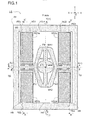
- Fig. 1 is a plan view of an optical scanner LS
- Fig. 2 is an enlarged view of a part of Fig. 1
- the optical scanner LS includes a mirror MR, a mirror axis MA, a movable frame FM, a frame axis FA, a holder HD, a piezoelectric element PE, torsion bars TB, and a fixing frame FF. These members are formed by etching a deformable silicon substrate or the like which serves as a base member BS.
- the mirror (moving portion) MR reflects light from a light source or the like, and is formed by attaching a reflective film of metal, aluminum, or the like to a part of the base member BS.
- a reflective film of metal, aluminum, or the like.
- a direction in which the first opening H1 and the second opening H2 are arrayed will be referred to as the X direction, and let the second opening H2 side of the X direction be plus ⁇ X (+) ⁇ of the X direction, and let the opposite direction with respect to the + direction be minus ⁇ (X (-) ⁇ of the X direction. Furthermore, a direction extending in the X direction from the center of the mirror MR will be referred to as the X axis.
- the mirror axis (a first axis portion) MA - an axial portion - is so created as to connect to one end and the other end of the mirror MR.
- One mirror axis MA (a first mirror axis MA1) connected to one end of the mirror MR and the other mirror axis MA (a second mirror axis MA2) connected to the other end of the mirror MR extend from the mirror MR in directions different from each other (note that the first mirror axis MA1 and the second mirror axis MA2 are parallel).
- the direction in which the mirror axis MA extends is orthogonal to (intersects with) the X direction.
- a direction in which the mirror axis MA extends will be refereed to as the Y direction, and let the first mirror axis MA1 side of the Y direction be plus ⁇ Y ⁇ +) ⁇ of the Y direction, and let the opposite direction with respect to the + direction be minus ⁇ (Y ⁇ -) ⁇ of the Y direction.
- a direction extending in the Y direction from the center of the mirror MR will be referred to as the Y axis.
- the direction orthogonal to the X direction and the Y direction be the Z direction (a warping direction), and, for the sake of convenience, let a light receiving side of the mirror MR be plus ⁇ Z (+) ⁇ of the Z direction, and let the opposite direction with respect to the + direction be minus ⁇ (Z (-) ⁇ of the Z direction.
- a direction extending in the Z direction from the point of intersection of the X axis and the Y axis will be referred to as the Z axis.
- the movable frame FM is a frame surrounding the mirror MR and the mirror axis MA.
- two openings H forming one opening H - a third opening H3 - so as to surround the first mirror axis MA1 and forming the other opening H - a fourth opening H4 - so as to surround the second mirror axis MA2 creates two remaining portions of the base member BS, specifically a remaining portion which is sandwiched by the third opening H3 and the first and second openings H1 and H2, and a remaining portion which is sandwiched by the fourth opening H4 and the first and second openings H1 and H2. Then, those two remaining portions serve as a frame shaped part of the base member BS that surrounds the mirror MR and the mirror axis MA, namely the movable frame FM.
- the frame axis (a second axis portion) FA holds the movable frame FM, at the outer periphery thereof, by extending outward from one end and the other end of the movable frame FM that coincide with the X axis and are opposite from each other.
- the bracket like third and fourth openings H3 and H4 are oppositely located and when both ends of the third opening H3 and both ends of the fourth opening H4 are oppositely located, parts of the base member BS sandwiched by those both ends have a bar shape, and that bar shaped parts serve as the frame axis FA.
- first frame axis FA1 one part of the frame axis FA extending toward the X (+) side
- second frame axis FA2 one part of the frame axis FA extending toward the X (+) side
- the holder HD holds the frame axis FA (the holder HD is connected to the frame axis FA) to thereby hold the movable frame FM.
- This holder HD is formed by a remaining portion of the base member BS which is created between openings H (a fifth opening H5 and a sixth opening H6) extending in the Y direction and the third and fourth openings H3 and H4.
- the fifth opening H5 and the sixth opening H6 are arrayed along the X direction, and sandwich the third and fourth openings H3 and H4. Then, a remaining portion of the base member BS which is located between the fifth opening H5 and the third and fourth openings H3 and H4 and extending in the Y direction serves as a first holder HD1, and a remaining portion of the base member BS which is located between the sixth opening H6 and the third and fourth openings H3 and H4 and extending in the Y direction serves as a second holder HD2. Note that such a holder HD with a shape (a linear shape) extending in the Y direction tends to warp.
- the piezoelectric element PE (PEa to PEd) is an element converting a voltage into a force.
- the piezoelectric element PE includes a piezoelectric member PB (PBa to PBd) that has been subjected to polarization treatment and electrodes EE1 and EE2 (EE1a to EE1d and EE2a to EE2d) that sandwich the piezoelectric member PB (see Figs 3 and 4 described below).
- a drive portion PE attached on the surface of the holder HD, a unimorph (an actuator) YM is formed.
- the unimorph YM (YMa to YMd) is formed.
- the piezoelectric member PB expands and contracts, and, according to the expansion and the contraction, the unimorph YM warps.
- the piezoelectric elements PEa and PEb are attached to the first holder HD1 so as to sandwich the first frame axis FA1.
- the piezoelectric elements PEc and PEd are attached to the second holder HD2 so as to sandwich the second frame axis FA2.
- the holder HD in response to deformation of expansion/contraction of the piezoelectric members PB (PBa to PBd) in the piezoelectric elements PEa and PEb and the piezoelectric elements PEc and PEd, the holder HD also is deformed (warps to be deformed or bends to be deformed).
- one strip of the first holder HD1 to which the piezoelectric element PEa is attached be a holding strip HD1a
- one strip of the first holder HD1 to which the piezoelectric element PEb is attached be a holding strip HD1b
- one strip of the second holder HD2 to which the piezoelectric element PEc is attached be a holding strip HD2c
- one strip of the second holder HD2 to which the piezoelectric element PEd is attached be a holding strip HD2d.
- the torsion bars TB are members for changing the deformation (warping deformation or the like) of the holder HD into twisting deformation (rotational torque) and transmitting it to the frame axis FA (see parts indicated by dotted lines in Figs. 1 and 2 ). These torsion bars TB are formed in the holder HD.
- parts of the base member BS serve as the torsion bars TB, the parts being located between first slits ST1 and ST1 extending in the X direction from ends of the third and fourth openings H3 and H4 and second slits ST2 and ST2 extending in the same direction (the X direction) as the first slits ST1 and ST1 and arrayed in parallel along the Y direction.
- Another parts of the base member BS serve as the torsion bars TB, the parts being located between third slits ST3 connected to the fifth opening H5, specifically, third slits ST3 extending in the X direction and arranged in lines with the first slits ST1 in the X direction and the second slits ST2.
- those torsion bars TB extend in a direction (for example in the X direction) intersecting with the direction (the Y direction) in which the holder HD extends. This makes it easier for the torsion bars TB to twist in a case where the holder HD warps.
- a part BS1 of the base member BS which is located between the first slits ST1 and ST1 is connected to the frame axis FA.
- a part BS3 of the base member BS which is located between the third slits ST3 and ST3 is arranged along the axis direction of the frame axis FA.
- those two parts BS1 and BS3 and a part BS M of the base member BS which is located between the two parts BS1 and BS3 may be collectively referred to as the frame axis FA.
- parts of the base member BS which is located between the part BS M and the second slits ST2 connect the torsion bars TB and the frame axis FA.
- those parts are referred to as connecting portions CB.
- the fixing frame FF is an outer frame of the optical scanner LS. Specifically, the fixing frame FF is a frame shaped member surrounding the mirror MR, the mirror axis MA, the movable frame FM, the frame axis FA, the holder HD, the piezoelectric element PE, and the torsion bars TB.
- the mirror MR is swingable (rotatetable) with respect tothe frame axis FA, and in addition the mirror MR is swingable with respect tothe mirror axis MA.
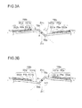
- a description will be given of the swinging of the mirror MR with respect tothe frame axis FA (the X axis) using Fig. 1 , and Figs. 3A and 3B which are cross sectional views taken along line A - A' in Fig. 1 .
- Fig. 3A shows the deformation of the first holder HD1 in a case where the mirror MR rotates in the normal direction
- Fig. 3B shows the deformation of the first holder HD1 in a case where the mirror MR rotates in the reverse direction.
- the first holder HD1 alone which is one of the two holders HD
- the other second holder HD2 deforms in a similar manner, i.e., rotates the mirror MR in the normal direction or in the reverse direction.
- a voltage for expanding the piezoelectric member PBa is applied, and in addition a voltage (a voltage of opposite phase from the voltage applied to the piezoelectric member PBa) for contracting the piezoelectric member PBb is applied.
- expansion of the piezoelectric member PBa causes the holding strip HD1a - to which the first electrode EE1a is attached - of the first holder HD1 to warp so as to bulge toward the Z (+) side. Consequently, the first frame axis FA1 side of the holding strip HD1a sags toward Z (-).
- contraction of the piezoelectric member PBb causes the holding strip HD1b - to which the first electrode EE1b is attached - of the first holder HD1 to warp so as to bulge toward the Z (-) side. Consequently, the first frame axis FA1 side of the holding strip HD1b springs up toward Z (+).
- the Y (+) side of the first frame axis FA1 is pushed down via the torsion bars TB (TBa), and the Y (-) side of the first frame axis FA1 is pushed up via the torsion bars TB (TBb).
- the torsion bars TBa and TBb easily twist with respect totheir axis directions (the bar axis directions), and the first frame axis FA1 is displaced.
- the mirror MR rotates with respect tothe frame axis FA in the normal direction.
- a voltage for contracting the piezoelectric member PBa is applied, and in addition a voltage for expanding the piezoelectric member PBb is applied.
- contraction of the piezoelectric member PBa causes the holding strip HD1a - to which the first electrode EE1a is attached - to warp so as to bulge toward the Z (-) side. Consequently, the first frame axis FA1 side of the holding strip HD1a springs up toward Z (+).
- expansion of the piezoelectric member PBb causes the holding strip HD1b - to which the first electrode EE1b is attached - to warp so as to bulge toward the Z (+) side. Consequently, the first frame axis FA1 side of the holding strip HD1b sags toward Z (-).
- the Y (+) side of the first frame axis FA1 is pushed up via the torsion bars TBa, and the Y (-) side of the first frame axis FA1 is pushed down via the torsion bars TBb.
- This displaces the first frame axis FA1 reversely with respect to the case where the first frame axis FA1 is rotated in the normal direction.
- the mirror MR rotates with respect tothe frame axis FA in the reverse direction.
- the mirror MR is swung (rotated in the normal direction or in the reverse direction) by utilizing the twisting deformation of the torsion bars TB which facilitates swinging of the frame axis FA and the warping of the holding strips HD1a and HD1b (namely the holder HD).
- the amount of swinging (a rotation angle ⁇ of normal rotation or reverse rotation) of such a frame axis FA is large (in other words, the amount of swinging of the frame axis FA is efficiently ensured) as compared with a case where the frame axis FA is swung by use of the warping of the holder HD alone.
- Figs. 4A and 4B show deformation of the first and second holders HD1 and HD2 in a case where the mirror MR rotates in the normal direction.
- Figs. 4C and 4D show deformation of the first and second holders HD1 and HD2 in a case where the mirror MR rotates in the reverse direction. Note that Figs. 4A and 4C are cross sectional views taken along line A - A' in Fig. 1 , and Figs. 4B and 4D are cross sectional views taken along line B - B' in Fig. 1 .
- a voltage for expanding the piezoelectric members PBa and PBb in the piezoelectric elements PEa and PEb is applied.
- both the holding strip HD1a - to which the first electrode EE1a is attached - of the first holder HD1 and the holding strip HD1b - to which the first electrode EE1b is attached - of the first holder HD1 warp so as to bulge toward the Z (+) side. Consequently, the first frame axis FA 1 sides of the holding strip HD1a and the holding strip HD1b sag toward Z (-), and the first frame axis FA1 is displaced toward Z (-) also.
- a voltage for contracting the piezoelectric members PBc and PBd in the piezoelectric elements PEc and PEd is applied.
- both the holding strip HD2c - to which the first electrode EE1c is attached - of the second holder HD2 and the holding strip HD2d - to which the first electrode EE1d is attached - of the second holder HD2 warp so as to bulge toward the Z (-) side. Consequently, the second frame axis FA2 sides of the holding strip HD2c and the holding strip HD2d spring up toward Z (+), and the second frame axis FA2 is displaced toward Z (+) also.
- the movable frame FM held by the first frame axis FA1 and the second frame axis FA2 tilts.
- the mirror MR included in the movable frame FM also tilts with respect tothe mirror axis MA. This tilting is caused by the displacements of the first frame axis FA1 and the second frame axis FA2 that are located away, approximately at equal intervals, from the mirror axis MA.
- the mirror MR rotates with respect tothe mirror axis MA in the normal direction.
- a voltage for contracting the piezoelectric members PBa and PBb of the piezoelectric elements PEa and PEb is applied.
- the holding strip HD1a and the holding strip HD1b in the first holder HD1 warp so as to bulge toward the Z (-) side. Consequently, the first frame axis FA1 sides of the holding strip HD1a and the holding strip HD1b spring up toward Z (+), and the first frame axis FA1 is displaced toward Z (+) also.
- a voltage for expanding the piezoelectric members PBc and PBd of the piezoelectric elements PEc and PEd is applied.
- the holding piec HD2c and the holding strip HD2d in the second holder HD2 warp so as to bulge toward the Z (+) side. Consequently, the second frame axis FA2 sides of the holding strip HD2 and the holding strip HD2d sag toward Z (-), and the second frame axis FA2 is displaced toward Z (-) also.
- the movable frame FM tilts, and in turn the mirror MR rotates with respect tothe mirror axis MA in the reverse direction.
- the rotation angles ⁇ (the inclination angles ⁇ ) of the normal/reverse rotations of the mirror MR with respect to the mirror axis MA - the Y axis - as described above is comparatively small.
- the frequency of the voltage applied to the piezoelectric element PE (PEa to PEd) for tilting the movable frame FM is the frequency around the resonance frequency of rotational vibration of the mirror MR with respect tothe mirror axis MA.
- the optical scanner LS includes the mirror axis MA and the frame axis FA having axis directions different from each other; the holder HD that is deformed in order to displace those two axes MA and FA; the piezoelectric element PE that generates, in response to a voltage applied thereto, a force for deforming the holder HD; and the mirror MR swinging, on one hand, with respect tothe mirror axis MA according the displacement of the mirror axis MA and, on the other hand, with respect to the frame axis FA according to the displacement of the frame axis FA.
- the mirror axis MA is displaced by resonating it in response to the frequency of the voltage applied to the piezoelectric element PE, whereas the frame axis FA is displaced by the deformation of the holder HD alone.
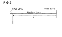
- a model system of a cantilever beam shown in Fig. 5 is taken up as an example.
- a side of the holding strip HD1a which is connected to the fixing frame FF is a fixed end
- a side of the holding strip HD1a which is close to the first frame axis FA1 is a free end.
- Equation (1) becomes the following niequation (3).
- EIv ⁇ ⁇ ⁇ + ⁇ A ⁇ ⁇ 2 ⁇ V 0
- first to fourth vibration models are represented by the following equations (13) to (16).
- the lengths of the cantilever beam in the first to fourth vibration modes are derived.
- a Young's modulus of 130 GPa, a density of 2300 kg/m 3 , and a cross sectional area of 0.2 mm 2 are set as the material physical properties of the cantilever beam to calculate the length L [mm] of the cantilever beam required at resonance frequencies of 10kHz, 20 kHz, and 30 kHz, the following Table 1 is obtained.
- the length L of the cantilever beam needs to be short (it is considered that the cantilever beam corresponds to the holding strip HD1a, the holding strip HD1b, the holding strip HD2a, and the holding strip HD2b).
- the cantilever beam has a comparatively short length L, it is generally less likely to warp (for example, the displacement of the free end of the cantilever beam tends to be small).
- the required displacement amount of the frame axis FA that is, the displacement amount of the first frame axis FA1 sides of the holding strip HD1a and the holding strip HD1b and the displacement amount of the second frame axis FA2 sides of the holding strip HD2a and the holding strip HD2b are comparatively small.
- the length of the holder HD (the holding strip HD1a, the holding strip HD1b, the holding strip HD2a, the holding strip HD2b) is short, although the mirror MR scans with respect tothe mirror axis MA at high speed, the rotation angle ⁇ of mirror MR with respect tothe frame axis FA is small. To overcome such an inconvenience, the length of the holder HD may be increased. However, if the holder HD is long, it is impossible for the mirror MR to swing with respect tothe mirror axis MA at high speed.
- the holder HD - the cantilever beam - needs to fulfill contradictory requirements in order to rotate the mirror MR with respect tothe frame axis FA comparatively greatly without resonance, and to swing the mirror MR with respect tothe mirror axis MA at high speed and at a great rotation angle.
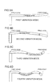
- Figs 7A to 7D are diagrams in which the displacement amounts of the cantilever beam in different first to fourth vibration modes in a case where the cantilever beam resonates at about 30 kHz is graphed, even though the cantilever beam is comparatively long, the displacement amount of the free end of the cantilever beam in the second to fourth vibration modes (multiple order vibration modes) with nodes is larger than the displacement amount of the free end of the cantilever beam in the first vibration mode without node.
- the mirror MR scan with respect tothe mirror axis MA at high speed, even though the holder HD is comparatively long in order to secure the angle of rotation - rotation without resonance with respect tothe frame axis FA - of the mirror MR.
- the optical scanner LS resonates at the frequency of the voltage applied to the piezoelectric element PE, preferably, that frequency vibrates the holder HD such that at least one node is generated that intersects with respect to the length of the holder HD itself.
- the frequency of the voltage applied to a piezoelectric element PE is approximate to or equal to the natural frequency of the optical scanner LS (a system including a mirror axis MA, a frame axis FA, a holder HD, a piezoelectric element PE, a mirror MR and a fixing frame FF).
- the mirror MR swings with respect tothe mirror axis MA comparatively greatly (in short, a great rotation angle is obtained).
- the natural frequency of the optical scanner LS is approximate to or equal to the natural frequency of a unimorph YM (a system including a holder HD and a piezoelectric element PE).
- a unimorph YM a system including a holder HD and a piezoelectric element PE.
- a drive portion of a piezoelectric system is not limited to a unimorph; it may be a bimorph.
- a member (a drive portion) that deforms the holder HD is not limited to the piezoelectric element PE.
- an electromagnetic unit 33 formed of an electromagnetic coil 31 and a permanent magnet 32 may serve as the drive portion (may serve as the drive portion of the electromagnetic system).
- Such an electromagnetic unit 33 has the electromagnetic coil 31 located on one face (the obverse face) of the holder HD, and has the permanent magnet 32 located at the rear side (to be apart from the reverse face of the holder HD) of the holder HD, so as to warp the holder HD by the electromagnetic force produced by the electromagnetic coil 31 and the permanent magnet 32.
- an electrostatic unit formed of two electrodes may serve as the drive portion (may serve as the drive portion of an electrostatic system).
- Such an electrostatic unit has one electrode located on the reverse face of the holder HD, and has the other electrode located apart from the reverse face of the holder HD (at the rear side of the holder HD), so as to warp the holder HD by the electrostatic force produced by the two electrodes.
- the drive portion may be of any of the electromagnetic system, the electrostatic system, the piezoelectric system, and another system, so long as it is able to deform the holder HD.
- the frequency of the voltage applied to the electrodes is approximate to or equal to the natural frequency of the optical scanner LS (a system including the mirror axis MA, the frame axis FA, the holder HD, the mirror MR, and the fixing frame FF).
- the natural frequency of the optical scanner LS is preferably approximate to the natural frequency of the holder HD. The reason for this is that, like in the case where the drive portion is the unimorph YM, the mirror MR swings with respect tothe mirror axis MA comparatively greatly.
- a two dimensional optical scanner LS is taken up as an example. This, however, is not meant to be any limitation; for example, the optical scanner LS may be a one dimensional optical scanner LS as shown in Fig. 9 .
- a mirror MR is directly connected to a holder HD via a mirror axis MA.
- the optical scanner LS includes the mirror axis (an axis portion) MA, the holder HD that is deformed in order to displace the mirror axis MA, a piezoelectric element PE that generates, in response to a voltage applied thereto, a force for deforming the holder HD, and the mirror MR that swings with respect tothe mirror axis MA according to the displacement of the mirror axis MA.
- the displacement of the mirror axis MA is caused by resonance, and the frequency of the voltage applied to the piezoelectric element PE is a frequency around the resonance frequency of the rotation vibration of the mirror MR.
- the frequency of the applied voltage that causes resonance is also a frequency that generates in the holder HD at least one node that intersects with respect to the length of the holder HD itself.
- the frequency of the voltage applied to the piezoelectric element PE is preferably approximate to or equal to the natural frequency of the optical scanner LS (a system including the mirror axis MA, the holder HD, the piezoelectric element PE, the mirror MR, and a fixing frame FF).
- the natural frequency of the optical scanner LS is approximate to the natural frequency of a unimorph YM. The reason for this is that the mirror MR swings with respect tothe mirror axis MA comparatively greatly.
- a drive portion may be of an electrostatic system.
- the frequency of the voltage applied to electrodes is approximate to or equal to the natural frequency of the optical scanner LS (a system including the mirror axis MA, the holder HD, the mirror MR, and the fixing frame FF).
- the natural frequency of the optical scanner LS is approximate to the natural frequency of the holder HD. The reason for this is that, as in the case where the drive portion is the unimorph YM, the mirror MR swings with respect tothe mirror axis MA comparatively greatly.
- the optical scanners LS described above are provided in micro scanner devices (optical devices) which various types are assumed (such micro scanner devices include a drive circuit that applies a voltage to a piezoelectric element PE).
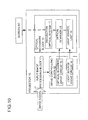
- a projector (an image projector) as shown in a block diagram of Fig. 10 is taken up as an example of the micro scanner devices.
- the projector 10 shown in Fig. 10 includes an inpu image processing block 11, a drive controlling block 12, and an optical mechanism block 15.
- the inpu image processing block 11 receives an image signal (such as a NTSC signal) transmitted from a personal computer (PC) or the like. Then, the inpu image processing block 11 applies, as necessary, correction ( ⁇ correction, distortion correction of an image, or the like) to the received image signal, and transmits the corrected image signal to the drive controlling block 12.
- an image signal such as a NTSC signal
- PC personal computer
- correction ⁇ correction, distortion correction of an image, or the like
- the drive controlling block 12 is configured with dedicated electronic circuitry, and includes an optical scanner drive circuit (a drive circuit) 13 and a light source drive circuit 14.
- the optical scanner drive circuit 13 generates a control signal for controlling the driving timing of an optical scanner LS to correspond to a vertical synchronizing signal and a horizontal synchronizing signal of the transmitted image signal. Then, the optical scanner drive circuit 13 transmits a drive signal of a potential corresponding to the control signal to the optical scanner LS included in the optical mechanism block 15.
- the optical scanner drive circuit 13 applies to a piezoelectric element PE a voltage having a frequency that is approximate to or equal to the natural frequency of the optical micro scanner LS itself and that generates in a holder HD at least one node that intersects with respect to the length of the holder HD.
- the light source drive circuit 14 controls light emission of a later described light source unit 16 (specifically, a light emitting block included in the light source unit 16) included in the optical mechanism block 15. Specifically, the light source drive circuit 14 makes the light source unit 16 emit light having color and luminance according to the gradation of the transmitted image signal. The timing for making the light source unit 16 illuminate corresponds to the vertical synchronizing signal and the horizontal synchronizing signal of the image signal.
- the optical mechanism block 15 includes the light source unit 16, the optical scanner LS, and a projection optical system 17, and projects light onto a screen SC (a projecting surface).
- the light source unit 16 includes, for example, a group of light emitting blocks where light emitting blocks such as lasers gather and a group of collimator lenses where collimator lenses that convert light from the light emitting blocks into an approximately parallel bundle of rays gather.
- the group of light emitting blocks includes a red light emitting block, a green light emitting block, and a blue light emitting block.
- the group of collimator lenses includes three collimator lenses to correspond to the light emitting blocks of different colors. Each light emitting block generates and emits a laser beam with a luminance according to a pixel value of a pixel signal from the light source drive circuit 14.
- the optical scanner LS is the optical scanner LS itself described above.
- the optical scanner LS has a mirror MR that reflects light traveling from the light source unit 16 and, by rotating the mirror MR with respect totwo respective axes (a mirror axis MA and a frame axis FA) that are substantially orthogonal to each other, reflects light two dimensionally to deflect it (scan).
- the projection optical system 17 leads, as necessary, the light deflected by the optical scanner LS onto the screen SC - the projecting surface - to project a moving image onto the screen SC.
- a dotted line arrow indicates light (a laser beam) from the light source unit 16 to the optical scanner LS, further to the projection optical system 17, and reaching the screen SC.
- a micro scanner device other than a projector 10 as shown in Fig. 10
- an image forming apparatus such as a copier and a printer.
- a micro scanner device it is possible to realize high speed scanning and provision of high resolution images.
- micro scanners other than optical scanners include those that are provided with, instead of a mirror MR, a lens (a refraction optical system) or a light source (a light emitting block).
Landscapes
- Physics & Mathematics (AREA)
- General Physics & Mathematics (AREA)
- Optics & Photonics (AREA)
- Engineering & Computer Science (AREA)
- Computer Hardware Design (AREA)
- Microelectronics & Electronic Packaging (AREA)
- Electromagnetism (AREA)
- Mechanical Optical Scanning Systems (AREA)
- Mechanical Light Control Or Optical Switches (AREA)
- Micromachines (AREA)
Applications Claiming Priority (2)
| Application Number | Priority Date | Filing Date | Title |
|---|---|---|---|
| JP2008002780 | 2008-01-10 | ||
| PCT/JP2008/073182 WO2009087883A1 (ja) | 2008-01-10 | 2008-12-19 | マイクロスキャナ装置およびマイクロスキャナ装置の制御方法 |
Publications (3)
| Publication Number | Publication Date |
|---|---|
| EP2233961A1 true EP2233961A1 (de) | 2010-09-29 |
| EP2233961A4 EP2233961A4 (de) | 2011-08-24 |
| EP2233961B1 EP2233961B1 (de) | 2016-02-17 |
Family
ID=40853007
Family Applications (1)
| Application Number | Title | Priority Date | Filing Date |
|---|---|---|---|
| EP08869942.6A Not-in-force EP2233961B1 (de) | 2008-01-10 | 2008-12-19 | Mikroscanner und verfahren zur steuerung eines mikroscanners |
Country Status (4)
| Country | Link |
|---|---|
| US (1) | US8717652B2 (de) |
| EP (1) | EP2233961B1 (de) |
| JP (1) | JP5310566B2 (de) |
| WO (1) | WO2009087883A1 (de) |
Cited By (3)
| Publication number | Priority date | Publication date | Assignee | Title |
|---|---|---|---|---|
| EP2803633A1 (de) | 2013-05-17 | 2014-11-19 | Fraunhofer-Gesellschaft zur Förderung der angewandten Forschung e.V. | Vorrichtung mit einem schwingfähig aufgehängten optischen Element |
| EP2808719A1 (de) * | 2013-05-28 | 2014-12-03 | Stanley Electric Co., Ltd. | Optischer Deflektor mit getrennten piezoelektrischen Abschnitten auf piezoelektrischen Aktuatoren und deren Entwurfsverfahren |
| EP4312070A1 (de) * | 2022-07-25 | 2024-01-31 | Ricoh Company, Ltd. | Bewegliche vorrichtung |
Families Citing this family (15)
| Publication number | Priority date | Publication date | Assignee | Title |
|---|---|---|---|---|
| EP2233961B1 (de) | 2008-01-10 | 2016-02-17 | Konica Minolta Opto, Inc. | Mikroscanner und verfahren zur steuerung eines mikroscanners |
| JP5381801B2 (ja) * | 2010-02-23 | 2014-01-08 | セイコーエプソン株式会社 | 画像形成装置 |
| JP5577742B2 (ja) | 2010-02-23 | 2014-08-27 | セイコーエプソン株式会社 | 光スキャナーおよび画像形成装置 |
| DE102010028111B4 (de) | 2010-04-22 | 2016-01-21 | Technische Universität Dresden | Mikromechanisches Element |
| JP5652336B2 (ja) * | 2011-06-06 | 2015-01-14 | 株式会社Jvcケンウッド | 光走査装置 |
| WO2012176492A1 (ja) * | 2011-06-21 | 2012-12-27 | コニカミノルタアドバンストレイヤー株式会社 | 共振駆動アクチュエーター、マイクロスキャナおよび光学機器 |
| JP6014234B2 (ja) * | 2012-05-10 | 2016-10-25 | パイオニア株式会社 | 駆動装置 |
| US9876418B2 (en) * | 2013-02-08 | 2018-01-23 | Pioneer Corporation | Actuator |
| DE102013210059B4 (de) | 2013-05-29 | 2021-07-01 | Fraunhofer-Gesellschaft zur Förderung der angewandten Forschung e.V. | Vorrichtung mit einer Feder und einem daran aufgehängten optischen Element |
| JP5867547B2 (ja) * | 2014-05-22 | 2016-02-24 | セイコーエプソン株式会社 | 光スキャナーおよび画像形成装置 |
| WO2018138193A1 (de) | 2017-01-27 | 2018-08-02 | Fraunhofer-Gesellschaft zur Förderung der angewandten Forschung e.V. | Mms, mms-array, mems-aktuator und verfahren zum bereitstellen eines mms |
| DE102017011821B4 (de) * | 2017-01-27 | 2020-12-31 | Fraunhofer-Gesellschaft zur Förderung der angewandten Forschung e.V. | MMS, MMS-Array, MEMS-Aktuator und Verfahren zum Bereitstellen eines MMS |
| DE102017217653A1 (de) * | 2017-10-05 | 2019-04-11 | Robert Bosch Gmbh | Mikromechanisches Bauteil, Herstellungsverfahren für ein mikromechanisches Bauteil und Verfahren zum Anregen einer Bewegung eines verstellbaren Teils um eine Rotationsachse |
| CN111428413B (zh) * | 2020-03-31 | 2022-05-31 | 广西交科集团有限公司 | 连续梁分段抗弯刚度识别方法 |
| US20220057514A1 (en) * | 2020-08-24 | 2022-02-24 | Beijing Voyager Technology Co., Ltd. | Mirror assembly for light steering |
Citations (7)
| Publication number | Priority date | Publication date | Assignee | Title |
|---|---|---|---|---|
| US20050219674A1 (en) * | 2002-11-26 | 2005-10-06 | Brother Kogyo Kabushiki Kaisha | Optical scanning apparatus and image forming apparatus |
| JP2005308863A (ja) * | 2004-04-19 | 2005-11-04 | Ricoh Co Ltd | 偏向ミラー、光走査装置及び画像形成装置 |
| US20070070481A1 (en) * | 2004-03-26 | 2007-03-29 | Brother Kogyo Kabushiki Kaisha | Resonant optical scanner using vibrating body with optimized resonant frequency characteristics and image forming apparatus having the same |
| US20070146858A1 (en) * | 2005-12-27 | 2007-06-28 | Konica Minolta Holdings, Inc. | Optical deflector and light beam scanning apparatus |
| US20070171500A1 (en) * | 2006-01-25 | 2007-07-26 | Samsung Electronics Co., Ltd. | Micro mirror employing piezo actuator |
| US20070268544A1 (en) * | 2006-05-19 | 2007-11-22 | Konica Minolta Holdings, Inc., | Optical scanner and scanning type projector |
| US20070269199A1 (en) * | 2006-05-16 | 2007-11-22 | Omron Corporation | Driving device, optical scanning device, and object information detecting device |
Family Cites Families (5)
| Publication number | Priority date | Publication date | Assignee | Title |
|---|---|---|---|---|
| JPH10104543A (ja) * | 1996-09-30 | 1998-04-24 | Omron Corp | 光走査装置および方法 |
| US7529011B2 (en) | 2004-04-12 | 2009-05-05 | Ricoh Company, Ltd. | Deflector mirror with regions of different flexural rigidity |
| JP4691704B2 (ja) | 2005-04-13 | 2011-06-01 | 独立行政法人産業技術総合研究所 | 光走査装置 |
| KR100682958B1 (ko) | 2006-01-10 | 2007-02-15 | 삼성전자주식회사 | 2축 마이크로 스캐너 |
| EP2233961B1 (de) | 2008-01-10 | 2016-02-17 | Konica Minolta Opto, Inc. | Mikroscanner und verfahren zur steuerung eines mikroscanners |
-
2008
- 2008-12-19 EP EP08869942.6A patent/EP2233961B1/de not_active Not-in-force
- 2008-12-19 WO PCT/JP2008/073182 patent/WO2009087883A1/ja active Application Filing
- 2008-12-19 JP JP2009548878A patent/JP5310566B2/ja not_active Expired - Fee Related
- 2008-12-19 US US12/811,944 patent/US8717652B2/en not_active Expired - Fee Related
Patent Citations (7)
| Publication number | Priority date | Publication date | Assignee | Title |
|---|---|---|---|---|
| US20050219674A1 (en) * | 2002-11-26 | 2005-10-06 | Brother Kogyo Kabushiki Kaisha | Optical scanning apparatus and image forming apparatus |
| US20070070481A1 (en) * | 2004-03-26 | 2007-03-29 | Brother Kogyo Kabushiki Kaisha | Resonant optical scanner using vibrating body with optimized resonant frequency characteristics and image forming apparatus having the same |
| JP2005308863A (ja) * | 2004-04-19 | 2005-11-04 | Ricoh Co Ltd | 偏向ミラー、光走査装置及び画像形成装置 |
| US20070146858A1 (en) * | 2005-12-27 | 2007-06-28 | Konica Minolta Holdings, Inc. | Optical deflector and light beam scanning apparatus |
| US20070171500A1 (en) * | 2006-01-25 | 2007-07-26 | Samsung Electronics Co., Ltd. | Micro mirror employing piezo actuator |
| US20070269199A1 (en) * | 2006-05-16 | 2007-11-22 | Omron Corporation | Driving device, optical scanning device, and object information detecting device |
| US20070268544A1 (en) * | 2006-05-19 | 2007-11-22 | Konica Minolta Holdings, Inc., | Optical scanner and scanning type projector |
Non-Patent Citations (1)
| Title |
|---|
| See also references of WO2009087883A1 * |
Cited By (6)
| Publication number | Priority date | Publication date | Assignee | Title |
|---|---|---|---|---|
| EP2803633A1 (de) | 2013-05-17 | 2014-11-19 | Fraunhofer-Gesellschaft zur Förderung der angewandten Forschung e.V. | Vorrichtung mit einem schwingfähig aufgehängten optischen Element |
| US9733470B2 (en) | 2013-05-17 | 2017-08-15 | Fraunhofer-Gesellschaft Zur Foerderung Der Angewandten Forschung E.V. | Device comprising a vibratably suspended optical element |
| DE102013209234B4 (de) | 2013-05-17 | 2018-04-05 | Fraunhofer-Gesellschaft zur Förderung der angewandten Forschung e.V. | Vorrichtung mit einem schwingfähig aufgehängten optischen Element |
| EP2808719A1 (de) * | 2013-05-28 | 2014-12-03 | Stanley Electric Co., Ltd. | Optischer Deflektor mit getrennten piezoelektrischen Abschnitten auf piezoelektrischen Aktuatoren und deren Entwurfsverfahren |
| US9395536B2 (en) | 2013-05-28 | 2016-07-19 | Stanley Electric Co., Ltd. | Optical deflector including separated piezoelectric portions on piezoelectric actuators and its designing method |
| EP4312070A1 (de) * | 2022-07-25 | 2024-01-31 | Ricoh Company, Ltd. | Bewegliche vorrichtung |
Also Published As
| Publication number | Publication date |
|---|---|
| JP5310566B2 (ja) | 2013-10-09 |
| EP2233961B1 (de) | 2016-02-17 |
| EP2233961A4 (de) | 2011-08-24 |
| WO2009087883A1 (ja) | 2009-07-16 |
| US8717652B2 (en) | 2014-05-06 |
| JPWO2009087883A1 (ja) | 2011-05-26 |
| US20100277783A1 (en) | 2010-11-04 |
Similar Documents
| Publication | Publication Date | Title |
|---|---|---|
| EP2233961A1 (de) | Mikroscanner und verfahren zur steuerung eines mikroscanners | |
| US8395834B2 (en) | Deflecting mirror for deflecting and scanning light beam | |
| JP4984117B2 (ja) | 2次元光スキャナ、それを用いた光学装置および2次元光スキャナの製造方法 | |
| JP4574396B2 (ja) | 光偏向器 | |
| US7220009B2 (en) | Optical deflector | |
| TWI446000B (zh) | 微機電系統掃描微鏡 | |
| JP2007310196A (ja) | 光スキャナ及び走査型プロジェクタ | |
| CN101750734B (zh) | 振动镜部件 | |
| US8659811B2 (en) | Actuator, optical scanner and image forming device | |
| JP6031683B2 (ja) | 光学反射素子 | |
| US20080198433A1 (en) | Microscanner and optical equipment with the same | |
| JP2006227144A (ja) | 光走査装置及び画像表示装置 | |
| JP2008304553A (ja) | アクチュエータ、光スキャナおよび画像形成装置 | |
| JP2016001275A (ja) | 光スキャナ | |
| JP2009002978A (ja) | マイクロスキャナ及びそれを備えた光走査装置。 | |
| WO2009081858A1 (ja) | マイクロスキャナ装置、およびマイクロスキャナ装置の制御方法 | |
| JP2008111882A (ja) | アクチュエータ、光スキャナおよび画像形成装置 | |
| EP2757405A1 (de) | Elektronische Vorrichtung mit einer Projektorfunktion und einem vibrierenden Spiegelelement | |
| EP1840625B1 (de) | Aktuator mit mechanischem Filter | |
| US8094356B2 (en) | Light scanning device and image forming device | |
| JP2001075042A (ja) | 光偏向器 | |
| JP4910902B2 (ja) | マイクロスキャナ及びそれを備えた光走査装置。 | |
| JP2009122293A (ja) | 揺動体装置、光偏向器、及びそれを用いた光学機器 | |
| JP6648443B2 (ja) | 光偏向器、2次元画像表示装置、光走査装置及び画像形成装置 | |
| JP5092406B2 (ja) | アクチュエータ、光スキャナおよび画像形成装置 |
Legal Events
| Date | Code | Title | Description |
|---|---|---|---|
| PUAI | Public reference made under article 153(3) epc to a published international application that has entered the european phase |
Free format text: ORIGINAL CODE: 0009012 |
|
| 17P | Request for examination filed |
Effective date: 20100708 |
|
| AK | Designated contracting states |
Kind code of ref document: A1 Designated state(s): AT BE BG CH CY CZ DE DK EE ES FI FR GB GR HR HU IE IS IT LI LT LU LV MC MT NL NO PL PT RO SE SI SK TR |
|
| AX | Request for extension of the european patent |
Extension state: AL BA MK RS |
|
| DAX | Request for extension of the european patent (deleted) | ||
| A4 | Supplementary search report drawn up and despatched |
Effective date: 20110725 |
|
| RIC1 | Information provided on ipc code assigned before grant |
Ipc: G02B 26/10 20060101AFI20110719BHEP Ipc: G02B 26/08 20060101ALI20110719BHEP Ipc: B81B 3/00 20060101ALI20110719BHEP |
|
| 17Q | First examination report despatched |
Effective date: 20130425 |
|
| GRAP | Despatch of communication of intention to grant a patent |
Free format text: ORIGINAL CODE: EPIDOSNIGR1 |
|
| INTG | Intention to grant announced |
Effective date: 20150814 |
|
| GRAS | Grant fee paid |
Free format text: ORIGINAL CODE: EPIDOSNIGR3 |
|
| GRAA | (expected) grant |
Free format text: ORIGINAL CODE: 0009210 |
|
| AK | Designated contracting states |
Kind code of ref document: B1 Designated state(s): AT BE BG CH CY CZ DE DK EE ES FI FR GB GR HR HU IE IS IT LI LT LU LV MC MT NL NO PL PT RO SE SI SK TR |
|
| REG | Reference to a national code |
Ref country code: GB Ref legal event code: FG4D |
|
| REG | Reference to a national code |
Ref country code: CH Ref legal event code: EP |
|
| REG | Reference to a national code |
Ref country code: IE Ref legal event code: FG4D |
|
| REG | Reference to a national code |
Ref country code: AT Ref legal event code: REF Ref document number: 775911 Country of ref document: AT Kind code of ref document: T Effective date: 20160315 |
|
| REG | Reference to a national code |
Ref country code: DE Ref legal event code: R096 Ref document number: 602008042455 Country of ref document: DE |
|
| REG | Reference to a national code |
Ref country code: NL Ref legal event code: MP Effective date: 20160217 |
|
| REG | Reference to a national code |
Ref country code: LT Ref legal event code: MG4D |
|
| REG | Reference to a national code |
Ref country code: AT Ref legal event code: MK05 Ref document number: 775911 Country of ref document: AT Kind code of ref document: T Effective date: 20160217 |
|
| PG25 | Lapsed in a contracting state [announced via postgrant information from national office to epo] |
Ref country code: IT Free format text: LAPSE BECAUSE OF FAILURE TO SUBMIT A TRANSLATION OF THE DESCRIPTION OR TO PAY THE FEE WITHIN THE PRESCRIBED TIME-LIMIT Effective date: 20160217 Ref country code: FI Free format text: LAPSE BECAUSE OF FAILURE TO SUBMIT A TRANSLATION OF THE DESCRIPTION OR TO PAY THE FEE WITHIN THE PRESCRIBED TIME-LIMIT Effective date: 20160217 Ref country code: ES Free format text: LAPSE BECAUSE OF FAILURE TO SUBMIT A TRANSLATION OF THE DESCRIPTION OR TO PAY THE FEE WITHIN THE PRESCRIBED TIME-LIMIT Effective date: 20160217 Ref country code: NO Free format text: LAPSE BECAUSE OF FAILURE TO SUBMIT A TRANSLATION OF THE DESCRIPTION OR TO PAY THE FEE WITHIN THE PRESCRIBED TIME-LIMIT Effective date: 20160517 Ref country code: GR Free format text: LAPSE BECAUSE OF FAILURE TO SUBMIT A TRANSLATION OF THE DESCRIPTION OR TO PAY THE FEE WITHIN THE PRESCRIBED TIME-LIMIT Effective date: 20160518 |
|
| PG25 | Lapsed in a contracting state [announced via postgrant information from national office to epo] |
Ref country code: PT Free format text: LAPSE BECAUSE OF FAILURE TO SUBMIT A TRANSLATION OF THE DESCRIPTION OR TO PAY THE FEE WITHIN THE PRESCRIBED TIME-LIMIT Effective date: 20160617 Ref country code: NL Free format text: LAPSE BECAUSE OF FAILURE TO SUBMIT A TRANSLATION OF THE DESCRIPTION OR TO PAY THE FEE WITHIN THE PRESCRIBED TIME-LIMIT Effective date: 20160217 Ref country code: LV Free format text: LAPSE BECAUSE OF FAILURE TO SUBMIT A TRANSLATION OF THE DESCRIPTION OR TO PAY THE FEE WITHIN THE PRESCRIBED TIME-LIMIT Effective date: 20160217 Ref country code: PL Free format text: LAPSE BECAUSE OF FAILURE TO SUBMIT A TRANSLATION OF THE DESCRIPTION OR TO PAY THE FEE WITHIN THE PRESCRIBED TIME-LIMIT Effective date: 20160217 Ref country code: LT Free format text: LAPSE BECAUSE OF FAILURE TO SUBMIT A TRANSLATION OF THE DESCRIPTION OR TO PAY THE FEE WITHIN THE PRESCRIBED TIME-LIMIT Effective date: 20160217 Ref country code: AT Free format text: LAPSE BECAUSE OF FAILURE TO SUBMIT A TRANSLATION OF THE DESCRIPTION OR TO PAY THE FEE WITHIN THE PRESCRIBED TIME-LIMIT Effective date: 20160217 Ref country code: SE Free format text: LAPSE BECAUSE OF FAILURE TO SUBMIT A TRANSLATION OF THE DESCRIPTION OR TO PAY THE FEE WITHIN THE PRESCRIBED TIME-LIMIT Effective date: 20160217 |
|
| PG25 | Lapsed in a contracting state [announced via postgrant information from national office to epo] |
Ref country code: DK Free format text: LAPSE BECAUSE OF FAILURE TO SUBMIT A TRANSLATION OF THE DESCRIPTION OR TO PAY THE FEE WITHIN THE PRESCRIBED TIME-LIMIT Effective date: 20160217 Ref country code: EE Free format text: LAPSE BECAUSE OF FAILURE TO SUBMIT A TRANSLATION OF THE DESCRIPTION OR TO PAY THE FEE WITHIN THE PRESCRIBED TIME-LIMIT Effective date: 20160217 |
|
| REG | Reference to a national code |
Ref country code: FR Ref legal event code: PLFP Year of fee payment: 9 |
|
| REG | Reference to a national code |
Ref country code: DE Ref legal event code: R097 Ref document number: 602008042455 Country of ref document: DE |
|
| PG25 | Lapsed in a contracting state [announced via postgrant information from national office to epo] |
Ref country code: SK Free format text: LAPSE BECAUSE OF FAILURE TO SUBMIT A TRANSLATION OF THE DESCRIPTION OR TO PAY THE FEE WITHIN THE PRESCRIBED TIME-LIMIT Effective date: 20160217 Ref country code: CZ Free format text: LAPSE BECAUSE OF FAILURE TO SUBMIT A TRANSLATION OF THE DESCRIPTION OR TO PAY THE FEE WITHIN THE PRESCRIBED TIME-LIMIT Effective date: 20160217 Ref country code: RO Free format text: LAPSE BECAUSE OF FAILURE TO SUBMIT A TRANSLATION OF THE DESCRIPTION OR TO PAY THE FEE WITHIN THE PRESCRIBED TIME-LIMIT Effective date: 20160217 |
|
| PLBE | No opposition filed within time limit |
Free format text: ORIGINAL CODE: 0009261 |
|
| STAA | Information on the status of an ep patent application or granted ep patent |
Free format text: STATUS: NO OPPOSITION FILED WITHIN TIME LIMIT |
|
| PG25 | Lapsed in a contracting state [announced via postgrant information from national office to epo] |
Ref country code: BE Free format text: LAPSE BECAUSE OF FAILURE TO SUBMIT A TRANSLATION OF THE DESCRIPTION OR TO PAY THE FEE WITHIN THE PRESCRIBED TIME-LIMIT Effective date: 20160217 |
|
| 26N | No opposition filed |
Effective date: 20161118 |
|
| PGFP | Annual fee paid to national office [announced via postgrant information from national office to epo] |
Ref country code: DE Payment date: 20161213 Year of fee payment: 9 Ref country code: GB Payment date: 20161214 Year of fee payment: 9 Ref country code: FR Payment date: 20161111 Year of fee payment: 9 |
|
| PG25 | Lapsed in a contracting state [announced via postgrant information from national office to epo] |
Ref country code: SI Free format text: LAPSE BECAUSE OF FAILURE TO SUBMIT A TRANSLATION OF THE DESCRIPTION OR TO PAY THE FEE WITHIN THE PRESCRIBED TIME-LIMIT Effective date: 20160217 Ref country code: BG Free format text: LAPSE BECAUSE OF FAILURE TO SUBMIT A TRANSLATION OF THE DESCRIPTION OR TO PAY THE FEE WITHIN THE PRESCRIBED TIME-LIMIT Effective date: 20160517 |
|
| REG | Reference to a national code |
Ref country code: CH Ref legal event code: PL |
|
| PG25 | Lapsed in a contracting state [announced via postgrant information from national office to epo] |
Ref country code: MC Free format text: LAPSE BECAUSE OF FAILURE TO SUBMIT A TRANSLATION OF THE DESCRIPTION OR TO PAY THE FEE WITHIN THE PRESCRIBED TIME-LIMIT Effective date: 20160217 |
|
| REG | Reference to a national code |
Ref country code: IE Ref legal event code: MM4A |
|
| PG25 | Lapsed in a contracting state [announced via postgrant information from national office to epo] |
Ref country code: CH Free format text: LAPSE BECAUSE OF NON-PAYMENT OF DUE FEES Effective date: 20161231 Ref country code: LU Free format text: LAPSE BECAUSE OF NON-PAYMENT OF DUE FEES Effective date: 20161219 Ref country code: LI Free format text: LAPSE BECAUSE OF NON-PAYMENT OF DUE FEES Effective date: 20161231 |
|
| PG25 | Lapsed in a contracting state [announced via postgrant information from national office to epo] |
Ref country code: IE Free format text: LAPSE BECAUSE OF NON-PAYMENT OF DUE FEES Effective date: 20161219 |
|
| PG25 | Lapsed in a contracting state [announced via postgrant information from national office to epo] |
Ref country code: HU Free format text: LAPSE BECAUSE OF FAILURE TO SUBMIT A TRANSLATION OF THE DESCRIPTION OR TO PAY THE FEE WITHIN THE PRESCRIBED TIME-LIMIT; INVALID AB INITIO Effective date: 20081219 Ref country code: CY Free format text: LAPSE BECAUSE OF FAILURE TO SUBMIT A TRANSLATION OF THE DESCRIPTION OR TO PAY THE FEE WITHIN THE PRESCRIBED TIME-LIMIT Effective date: 20160217 |
|
| PG25 | Lapsed in a contracting state [announced via postgrant information from national office to epo] |
Ref country code: HR Free format text: LAPSE BECAUSE OF FAILURE TO SUBMIT A TRANSLATION OF THE DESCRIPTION OR TO PAY THE FEE WITHIN THE PRESCRIBED TIME-LIMIT Effective date: 20160217 Ref country code: IS Free format text: LAPSE BECAUSE OF FAILURE TO SUBMIT A TRANSLATION OF THE DESCRIPTION OR TO PAY THE FEE WITHIN THE PRESCRIBED TIME-LIMIT Effective date: 20160217 Ref country code: TR Free format text: LAPSE BECAUSE OF FAILURE TO SUBMIT A TRANSLATION OF THE DESCRIPTION OR TO PAY THE FEE WITHIN THE PRESCRIBED TIME-LIMIT Effective date: 20160217 |
|
| REG | Reference to a national code |
Ref country code: DE Ref legal event code: R119 Ref document number: 602008042455 Country of ref document: DE |
|
| GBPC | Gb: european patent ceased through non-payment of renewal fee |
Effective date: 20171219 |
|
| PG25 | Lapsed in a contracting state [announced via postgrant information from national office to epo] |
Ref country code: MT Free format text: LAPSE BECAUSE OF NON-PAYMENT OF DUE FEES Effective date: 20161219 |
|
| REG | Reference to a national code |
Ref country code: FR Ref legal event code: ST Effective date: 20180831 |
|
| PG25 | Lapsed in a contracting state [announced via postgrant information from national office to epo] |
Ref country code: FR Free format text: LAPSE BECAUSE OF NON-PAYMENT OF DUE FEES Effective date: 20180102 Ref country code: DE Free format text: LAPSE BECAUSE OF NON-PAYMENT OF DUE FEES Effective date: 20180703 |
|
| PG25 | Lapsed in a contracting state [announced via postgrant information from national office to epo] |
Ref country code: GB Free format text: LAPSE BECAUSE OF NON-PAYMENT OF DUE FEES Effective date: 20171219 |