EP2211368B1 - Teilchenoptische Komponente - Google Patents
Teilchenoptische Komponente Download PDFInfo
- Publication number
- EP2211368B1 EP2211368B1 EP10003918A EP10003918A EP2211368B1 EP 2211368 B1 EP2211368 B1 EP 2211368B1 EP 10003918 A EP10003918 A EP 10003918A EP 10003918 A EP10003918 A EP 10003918A EP 2211368 B1 EP2211368 B1 EP 2211368B1
- Authority
- EP
- European Patent Office
- Prior art keywords
- pole piece
- objective lens
- lens arrangement
- pole
- disposed
- Prior art date
- Legal status (The legal status is an assumption and is not a legal conclusion. Google has not performed a legal analysis and makes no representation as to the accuracy of the status listed.)
- Active
Links
Images


Classifications
-
- H—ELECTRICITY
- H01—ELECTRIC ELEMENTS
- H01J—ELECTRIC DISCHARGE TUBES OR DISCHARGE LAMPS
- H01J37/00—Discharge tubes with provision for introducing objects or material to be exposed to the discharge, e.g. for the purpose of examination or processing thereof
- H01J37/02—Details
- H01J37/04—Arrangements of electrodes and associated parts for generating or controlling the discharge, e.g. electron-optical arrangement or ion-optical arrangement
- H01J37/10—Lenses
- H01J37/14—Lenses magnetic
- H01J37/141—Electromagnetic lenses
-
- H—ELECTRICITY
- H01—ELECTRIC ELEMENTS
- H01J—ELECTRIC DISCHARGE TUBES OR DISCHARGE LAMPS
- H01J37/00—Discharge tubes with provision for introducing objects or material to be exposed to the discharge, e.g. for the purpose of examination or processing thereof
- H01J37/02—Details
- H01J37/04—Arrangements of electrodes and associated parts for generating or controlling the discharge, e.g. electron-optical arrangement or ion-optical arrangement
- H01J37/10—Lenses
- H01J37/145—Combinations of electrostatic and magnetic lenses
-
- H—ELECTRICITY
- H01—ELECTRIC ELEMENTS
- H01J—ELECTRIC DISCHARGE TUBES OR DISCHARGE LAMPS
- H01J37/00—Discharge tubes with provision for introducing objects or material to be exposed to the discharge, e.g. for the purpose of examination or processing thereof
- H01J37/02—Details
- H01J37/20—Means for supporting or positioning the object or the material; Means for adjusting diaphragms or lenses associated with the support
-
- H—ELECTRICITY
- H01—ELECTRIC ELEMENTS
- H01J—ELECTRIC DISCHARGE TUBES OR DISCHARGE LAMPS
- H01J37/00—Discharge tubes with provision for introducing objects or material to be exposed to the discharge, e.g. for the purpose of examination or processing thereof
- H01J37/02—Details
- H01J37/21—Means for adjusting the focus
-
- H—ELECTRICITY
- H01—ELECTRIC ELEMENTS
- H01J—ELECTRIC DISCHARGE TUBES OR DISCHARGE LAMPS
- H01J37/00—Discharge tubes with provision for introducing objects or material to be exposed to the discharge, e.g. for the purpose of examination or processing thereof
- H01J37/02—Details
- H01J37/24—Circuit arrangements not adapted to a particular application of the tube and not otherwise provided for
-
- H—ELECTRICITY
- H01—ELECTRIC ELEMENTS
- H01J—ELECTRIC DISCHARGE TUBES OR DISCHARGE LAMPS
- H01J37/00—Discharge tubes with provision for introducing objects or material to be exposed to the discharge, e.g. for the purpose of examination or processing thereof
- H01J37/26—Electron or ion microscopes; Electron or ion diffraction tubes
- H01J37/28—Electron or ion microscopes; Electron or ion diffraction tubes with scanning beams
-
- H—ELECTRICITY
- H01—ELECTRIC ELEMENTS
- H01J—ELECTRIC DISCHARGE TUBES OR DISCHARGE LAMPS
- H01J2237/00—Discharge tubes exposing object to beam, e.g. for analysis treatment, etching, imaging
- H01J2237/002—Cooling arrangements
-
- H—ELECTRICITY
- H01—ELECTRIC ELEMENTS
- H01J—ELECTRIC DISCHARGE TUBES OR DISCHARGE LAMPS
- H01J2237/00—Discharge tubes exposing object to beam, e.g. for analysis treatment, etching, imaging
- H01J2237/04—Means for controlling the discharge
- H01J2237/049—Focusing means
- H01J2237/0492—Lens systems
- H01J2237/04922—Lens systems electromagnetic
-
- H—ELECTRICITY
- H01—ELECTRIC ELEMENTS
- H01J—ELECTRIC DISCHARGE TUBES OR DISCHARGE LAMPS
- H01J2237/00—Discharge tubes exposing object to beam, e.g. for analysis treatment, etching, imaging
- H01J2237/04—Means for controlling the discharge
- H01J2237/049—Focusing means
- H01J2237/0492—Lens systems
- H01J2237/04926—Lens systems combined
-
- H—ELECTRICITY
- H01—ELECTRIC ELEMENTS
- H01J—ELECTRIC DISCHARGE TUBES OR DISCHARGE LAMPS
- H01J2237/00—Discharge tubes exposing object to beam, e.g. for analysis treatment, etching, imaging
- H01J2237/10—Lenses
- H01J2237/12—Lenses electrostatic
-
- H—ELECTRICITY
- H01—ELECTRIC ELEMENTS
- H01J—ELECTRIC DISCHARGE TUBES OR DISCHARGE LAMPS
- H01J2237/00—Discharge tubes exposing object to beam, e.g. for analysis treatment, etching, imaging
- H01J2237/10—Lenses
- H01J2237/12—Lenses electrostatic
- H01J2237/121—Lenses electrostatic characterised by shape
- H01J2237/1215—Annular electrodes
-
- H—ELECTRICITY
- H01—ELECTRIC ELEMENTS
- H01J—ELECTRIC DISCHARGE TUBES OR DISCHARGE LAMPS
- H01J2237/00—Discharge tubes exposing object to beam, e.g. for analysis treatment, etching, imaging
- H01J2237/10—Lenses
- H01J2237/14—Lenses magnetic
-
- H—ELECTRICITY
- H01—ELECTRIC ELEMENTS
- H01J—ELECTRIC DISCHARGE TUBES OR DISCHARGE LAMPS
- H01J2237/00—Discharge tubes exposing object to beam, e.g. for analysis treatment, etching, imaging
- H01J2237/10—Lenses
- H01J2237/14—Lenses magnetic
- H01J2237/1405—Constructional details
-
- H—ELECTRICITY
- H01—ELECTRIC ELEMENTS
- H01J—ELECTRIC DISCHARGE TUBES OR DISCHARGE LAMPS
- H01J2237/00—Discharge tubes exposing object to beam, e.g. for analysis treatment, etching, imaging
- H01J2237/10—Lenses
- H01J2237/14—Lenses magnetic
- H01J2237/1405—Constructional details
- H01J2237/141—Coils
-
- H—ELECTRICITY
- H01—ELECTRIC ELEMENTS
- H01J—ELECTRIC DISCHARGE TUBES OR DISCHARGE LAMPS
- H01J2237/00—Discharge tubes exposing object to beam, e.g. for analysis treatment, etching, imaging
- H01J2237/10—Lenses
- H01J2237/14—Lenses magnetic
- H01J2237/1405—Constructional details
- H01J2237/1415—Bores or yokes, i.e. magnetic circuit in general
-
- H—ELECTRICITY
- H01—ELECTRIC ELEMENTS
- H01J—ELECTRIC DISCHARGE TUBES OR DISCHARGE LAMPS
- H01J2237/00—Discharge tubes exposing object to beam, e.g. for analysis treatment, etching, imaging
- H01J2237/26—Electron or ion microscopes
- H01J2237/28—Scanning microscopes
- H01J2237/2813—Scanning microscopes characterised by the application
- H01J2237/2817—Pattern inspection
Definitions
- the present invention relates to an objective lens arrangement for use in particle-optical systems.
- the invention relates to a particle-optical beam system as well as a particle-optical inspection system.
- the invention may be applied to charged particles of any type, such as electrons, positrons, muons, ions (charged atoms or molecules) and others.
- the increasing demand for ever smaller and more complex microstructured devices and the continuing demand for an increase of a throughput in the manufacturing and inspection processes thereof have been an incentive for the development of particle-optical systems that use multiple charged particle beamlets in place of a single charged particle beam, thus significantly improving the throughput of such systems.
- the multiple charged particle beamlets may be provided by a single column using a multi-aperture array, for instance, or by multiple individual columns, or a combination of both, as will be described in more detail below.
- the use of multiple beamlets is associated with a whole range of new challenges to the design of particle-optical components, arrangements and systems, such as microscopes and lithography systems.
- a conventional particle-optical system is known from US 6,252,412 B1 .
- the electron microscopy apparatus disclosed therein is used for inspecting an object, such as a semiconductor wafer.
- a plurality of primary electron beams is focused in parallel to each other on the object to form a plurality of primary electron spots thereon. Secondary electrons generated by the primary electrons and emanating from respective primary electron spots are detected.
- For each primary electron beam a separate electron beam column is provided.
- the plurality of separate electron beam columns is closely packed.
- a density of the primary electron beam spots formed on the object is limited by a remaining footstep size of the electron beam columns forming the electron microscopy apparatus.
- the number of primary electron beam spots, which may be formed simultaneously on the object is also limited in practice, resulting in a limited throughput of the apparatus when inspecting semiconductor wafers of a high surface area at a high resolution.
- electron microscopy apparatus which use a plurality of primary electron beamlets focused onto the surface of the object to be inspected.
- the beamlets are generated by a multi-aperture plate having a plurality of apertures formed therein, wherein an electron source generating a single electron beam is provided upstream of the multi-aperture plate for illuminating the apertures formed therein.
- a plurality of electron beamlets is formed by those electrons of the electron beam that pass the apertures.
- the plurality of primary electron beamlets is focused on the object by an objective lens having an aperture, which is passed by all primary electron beamlets.
- An array of primary electron spots is then formed on the object. Secondary electrons emanating from each primary electron spot form a respective secondary electron beamlet, such that a plurality of secondary electron beamlets corresponding to the plurality of primary electron beam spots is generated.
- the plurality of secondary electron beamlets also pass the objective lens, and the apparatus provides a secondary electron beam path such that each of the secondary electron beamlets is supplied to a respective one of a plurality of detector pixels of a CCD electron detector.
- a Wien-filter is used for separating the secondary electron beam path from a beam path of the primary electron beamlets.
- one single electron-optical column may be employed, and the density of primary electron beam spots formed on the object is not limited by a foot step size of the single electron-optical column.
- the number of primary electron beam spots disclosed in the embodiments of the above-mentioned documents is in the order of some ten spots. Since the number of primary electron beam spots formed on the object at the same time limits the throughput, it is desirable to increase the number of primary electron beam spots in order to achieve a higher throughput. It has been found, however, that it is difficult to increase the number of primary electron beam spots formed at the same time, or to increase a primary electron beam spot density, employing the technology disclosed in those documents while maintaining a desired imaging resolution of the electron microscopy apparatus.
- the present invention is applicable to particle-optical systems using multiple beamlets of charged particles; the present invention is, however, not limited in the application to systems using multiple beamlets, but is equally applicable to particle-optical systems using only one single beam of charged particles.
- Embodiments of the present invention provide an objective lens arrangement having an object plane and an axis of symmetry and comprising first, second and third pole pieces which are substantially rotationally symmetric with respect to an axis of symmetry and which are disposed on a same side of the object plane.
- the first, second and third pole pieces extend towards the axis of symmetry such that radial inner ends of the first, second and third pole pieces each define a bore which is to be traversed by a beam path of one or more beams of charged particles.
- a radial inner end of the first pole piece is disposed at a distance from a radial inner end of the second pole piece to form a first gap between them, and a radial inner end of the third pole piece is disposed at a distance from the radial inner end of the second pole piece to form a second gap between them.
- the axis of symmetry referred to above generally coincides with the optical axis of a particle-optical system the objective lens arrangement is comprised in, such that the two terms are used to the same effect herein.
- the objective lens arrangement may also be described as having a central axis which may or may not also be an axis of symmetry, which central axis generally coincides with the optical axis of a system the objective lens arrangement is comprised in and thus also be used synonymously to the term optical axis.
- a first excitation coil is provided for generating a magnetic field in a region of the first gap, and a second excitation coil is provided for generating a magnetic field in a region of the second gap.
- a first power supply is provided for supplying an excitation current to the first excitation coil, and a second power supply is provided for supplying an excitation current to the second excitation coil.
- the first and second power supplies may be two portions of a same power supply.
- the first and second power supplies are configured to supply currents to the first and second excitation coils and thus generate excitation currents such that a magnetic flux generated by the first excitation coil in the second pole piece is oriented in the same or a different direction as a magnetic flux generated by the second excitation coil in the second pole piece.
- the first excitation coil is disposed between the first and second pole pieces and the second excitation coil disposed between the second and third pole pieces.
- the magnetic field generated in a region of the gap may have different magnetic field strengths and different dimensions.
- the magnetic field may extend only over a region close to the gap or may extend as far as the object plane. Since magnetic lenses are usually employed in inspection optical systems to provide a focusing effect, a magnetic focusing field generally extends as far as the object plane in order to achieve a good focusing effect, avoid defocusing before the object plane and avoid particle-optical aberrations.
- the objective lens arrangement according to this embodiment allows adjusting the magnetic fields in the first and second gaps such that the magnetic field in the first gap provides a focusing effect on the one or more beams of charged particles traversing the focusing magnetic field whilst the magnetic field generated in the second gap is configured to compensate for the focusing magnetic field extending from the first gap to locations on or at least close to the object plane.
- the first and second gaps may be disposed at an angle to one another, for instance.
- the angle formed between the first and second radial gaps may be in a range of from 10 to about 170 degrees, for instance, and may be in a range of from 45 to 135 degrees or from 60 to 120 degrees, by way of example.
- the first gap is disposed at an angle to the axis of symmetry that is different from an angle formed between the second gap and the axis of symmetry.
- a straight line connecting the radial inner ends of the respective pole pieces forming the gap may be employed to represent the gap.
- the first gap is oriented substantially in an axial direction, i.e. substantially parallel or at a relatively small angle to the axis of symmetry, and thus forms an axial gap.
- An axial gap does not necessarily imply that radial innermost ends of the pole pieces forming the gap need to have the same distance from the axis of symmetry, but also encompasses those embodiments wherein the innermost ends have different distances from the axis of symmetry and wherein the gap formed between points on radial inner ends of the pole pieces that are disposed closest to one another form an angle of less than 45°, for instance less than 30° or less than 15° to the axis of symmetry.
- the second gap may be oriented substantially in a radial direction with respect to the objective lens arrangement, i.e. orthogonal to the axis of symmetry and thus form a radial gap.
- Radial gaps also encompass those embodiments wherein the gap defined by a closest distance (straight line along the closest distance) between the inner radial ends of the pole pieces is disposed at an angle of from about 50° to 90° to the axis of symmetry, such as from about 80° to 90° to the axis of symmetry.
- the focusing magnetic field (generated in the first gap) is compensated for by the magnetic field generated in the second gap to such an extent that a total magnetic field in a region on the object plane and about the optical axis is substantially zero, in other words, the compensating magnetic field substantially cancels the focusing magnetic field in a region on the object plane.
- Such a configuration allows obtaining advantageous imaging properties with the objective lens arrangement.
- an image rotation caused by the focusing magnetic field may be eliminated in the vicinity of the object plane. This allows achieving improved overall performance of the system, in particular with regard to structured objects, which are inspected and/or processed using the objective lens arrangement.
- the configuration of, in particular, the embodiment with the first gap being an axial gap and the second gap being a radial gap is particularly advantageous, since the pole pieces can be arranged such that the radial inner end of the second pole piece is disposed close to the object plane such that the focusing magnetic field is also generated and disposed close to the object plane.
- having a radial gap formed between the inner radial end of the second pole piece, which also defines the lower end of the first gap, and the third pole piece allows the radial gap to be disposed close to the first gap and the focusing magnetic field to be generated close to the object plane, thus providing the magnetic field compensating effect in very close vicinity to the object plane.
- the radial orientation of the second gap also allows generating the compensating magnetic field downstream of the objective lens arrangement thus not interfering with the focusing magnetic field inside the objective lens arrangement and thus not impairing a focusing effect provided thereby.
- This embodiment thus advantageously allows the major portion of the focusing magnetic field to remain unaffected and enables the compensating field to take effect on/close to the object plane.
- the radial inner end of the third pole piece and the radial inner end of the second pole piece are disposed in substantially a same plane, which plane is disposed substantially parallel to the object plane.
- the objective lens arrangement may additionally comprise a fourth pole piece which is substantially rotationally symmetric with respect to the axis of symmetry, wherein a third gap is formed between the fourth pole piece and the first pole piece, and wherein the third gap is disposed at a greater distance from the object plane than the first gap; and a third excitation coil for generating an adjusting magnetic field in the third gap.
- the adjusting magnetic field may be used to adjust the focusing magnetic field in terms of its strength, location, dimension and other parameters.
- the adjusting magnetic field may be used to increase or decrease the focusing magnetic field strength, for instance.
- the fourth gap may be an axial gap, for example.
- the inner radial end of the fourth pole piece may be disposed at a distance from the axis of symmetry that is greater, equal to or smaller than a distance between the radial inner end of the first pole piece and the axis of symmetry, for instance.
- the pole pieces may be disposed and configured such that, for instance, the second and third pole pieces are electrically connected to each other and the first pole piece is electrically insulated from the second and third pole pieces, such as by an insulating layer.
- the insulating layer may be provided between an outer cylindrical portion of or integrally formed with the first pole piece and a substantially cylindrical yoke formed by and connecting the second and third pole pieces.
- the outer cylindrical portion may extend around and substantially parallel to the yoke as well as the axis of symmetry, for example, such that the insulating layer also extends substantially in an axial direction.
- the first pole piece may comprise an annular, substantially disc-shaped or disc-like portion or have an annular disc-shaped or disc-like portion integrally formed with it.
- the insulating layer may be provided between the outer annular disc shaped portion integrally formed with the first pole piece, and an outer portion of the second pole piece.
- the annular disc-shape or disc-like portion and the outer portion are arranged to have parallel surfaces over at least a portion thereof.
- the first pole piece comprises an inner member and an outer member, that is comprises two distinct parts, with the inner and outer members being electrically insulated from one another by an insulating layer.
- Inner and outer refer to a radial distance from the axis of symmetry, i.e. a distance from the axis of symmetry in a plane orthogonal to the axis of symmetry.
- an additional insulating layer may be provided between the outer member of the first pole piece and an outer portion of the second pole piece.
- the outer member of the first pole piece in this exemplary embodiment of the objective lens arrangement according to the present invention may be configured to accommodate the first excitation coil.
- the inner member of the first pole piece may comprise or consist of a substantially conical portion extending towards the axis of symmetry.
- the outer member may have or comprise a substantially annular shape, for instance.
- the invention provides an objective lens arrangement having an object plane and an axis of symmetry and comprising first and second pole pieces which are rotationally symmetric with respect to the axis of symmetry, with inner ends of the first and second pole pieces defining respective bores which are configured to be traversed by a beam path of one or more beams of charged particles.
- the radial inner end of the first pole piece is disposed at a distance from the radial inner end of the second pole piece to form a (first) gap between them, with the second pole piece being disposed closer to the object plane than the first pole piece.
- the first and second pole pieces are electrically insulated from each other.
- a first excitation coil is provided for generating a focusing magnetic field in the first gap, and a beam tube extends through the bore formed by the radial inner end of the first pole piece.
- the objective lens arrangement according to this embodiment further comprises an object mount for mounting an object to be processed such that the object is disposed in the object plane.
- the object mount includes an electrical connector for supplying an electrical voltage to the object to be processed.
- object to be processed is to be understood as encompassing objects that are inspected, imaged and/or manipulated by a charged particle beam or a plurality of charged particle beamlets.
- the objective lens arrangement according to this embodiment further comprises a first voltage source configured for supplying a voltage to the beam tube such that the beam tube is more than about 15 kV above ground potential.
- a second voltage source is provided and configured for supplying a voltage to the electrical connector such that the electrical connector is grounded or below ground potential.
- the second voltage source may be configured to supply a voltage such that the electrical connector is more than about 15 kV below ground potential.
- the objective lens arrangement further comprises a third voltage source configured for supplying a voltage to the second pole piece such that a potential of the second pole piece is from about 0.1 kV to about 10 kV above a potential of the electrical connector.
- the first through third voltage sources may be individual voltage sources or portions of a same voltage source.
- Such an arrangement allows to obtain advantageous optical properties of an electron microscopy system, for instance, using the objective lens arrangement since a primary electron beam having a particularly high kinetic energy may be generated and formed by beam shaping components of the electron microscopy system, and the primary electrons of the beam are decelerated to desired kinetic energies only shortly above the object plane, thus greatly reducing Coulomb interactions between the primary electrons. Further, an electrical field generated between the object disposed in the object plane and the second pole piece will accelerate secondary electrons emanating from the object.
- voltages supplied by the first or second voltage sources include voltages which may be equal to or higher than 20 kV, 25 kV, 30 kV and may be equal to or higher than 45 kV, for instance.
- the voltage supplied by the third voltage source may be an adjustable voltage, for instance, which allows precise adjustment of an electrical field immediately above the object plane to a desired value.
- the first and/or second voltage sources may be adjustable voltage sources.
- the beam tube is electrically insulated from the first pole piece.
- the first pole piece is substantially at ground potential.
- the third voltage source has one of its connectors connected to the second pole piece and another of its connectors connected to the electrical connector of the object mount, i.e. is connected to both the second pole piece and the electrical connector.
- the first pole piece is electrically insulated from the second and third pole pieces by a thin insulating layer.
- a large area of overlap is provided between the first pole piece on one side and the second or third pole pieces on the other side, in other words a large area is provided in which opposite surfaces of the respective pole pieces are arranged in the vicinity of one another and preferably parallel or nearly parallel to one another. This allows for a sufficient electrical insulation between the first pole piece and the second and third pole pieces whilst maintaining a sufficiently low magnetic resistance for generating the focusing magnetic field in the first gap.
- the insulating layer is preferably provided between an outer portion of the first pole piece and an outer portion of the second pole piece.
- the insulating layer is preferably provided between the cylindrical portion of the first pole piece and an outer portion of the second pole piece.
- the objective lens arrangement may further comprise a third pole piece having a radial inner end which is disposed at a distance from the radial inner end of the second pole piece to form a second gap, wherein the first pole piece is electrically insulated from both the second and third pole pieces by an insulating layer.
- the first pole piece comprises an inner member and an outer member, that is two separate parts, with the inner and outer members being electrically insulated from each other by an insulating layer.
- the outer member would then also comprise the outer portion of the pole piece that is generally disposed to face the outer portion of the second pole piece.
- the outer member of the first pole piece is configured to accommodate the first excitation coil and the inner member of the first pole piece comprises a substantially conical portion extending towards the axis of symmetry.
- Dividing the first pole piece into an inner member and an outer member and electrically connecting the inner member and the beam tube extending through the bore formed by the inner member has the advantage that provision of electrical power to the beam tube is facilitated. Rather than having to provide electrical wiring to the beam tube itself, the electrical power is provided via the inner member of the pole piece, which is more easily accessible for electrical connections.
- dividing the first pole piece into two members and electrically insulating the two members from one another saves the provision of an electrically insulating layer between the beam tube and the first pole piece, which tends to require a complex layout to avoid creep currents and the like.
- the invention provides an objective lens arrangement, comprising a second pole piece and a third pole piece, wherein the second and third pole pieces are substantially rotationally symmetric with respect to an axis of symmetry, wherein the second and third pole pieces are disposed on a same side of an object plane of the objective lens arrangement, wherein a radial inner end of the third pole piece is disposed at a distance from a radial inner end of the second pole piece to form a second gap, and wherein the second and third pole pieces are electrically connected to each other; a second excitation coil for generating a magnetic field in the second gap; and a second power supply configured for supplying an excitation current to the second excitation coil, wherein the second power supply is substantially at ground potential; and a third voltage source configured for supplying a voltage to the second pole piece such that the second pole piece is at a potential differing from a potential of the second excitation coil by more than 15 kV, in particular more than 20 kV, in particular more than 25 kV, and in particular more than
- pole pieces of the objective lens arrangement according to of the invention are denoted “second” and “third” pole pieces (rather than “first” and “second”) simply for sake of clarity and easier reference to other embodiments and aspects of the present invention as described herein, the same applies to the numbering of the power supplies.
- the second pole piece may be advantageously used for shaping the electrical field in a region close to the object plane whilst, at the same time, avoiding to operate the power supply for supplying the excitation current to the second excitation coil at a high electrical potential.
- the objective lens arrangement according to the present invention further comprises: a first pole piece, wherein the first pole piece is substantially rotationally symmetric with respect to the axis of symmetry, wherein the first pole piece is disposed on the same side of the object plane of the objective lens arrangement as the second and third pole pieces, wherein a radial inner end of the first pole piece is disposed at a distance from the radial inner end of the second pole piece to form a first gap, and wherein the first pole piece is electrically insulated from the second and third pole pieces, wherein the third voltage source is further configured to supply the voltage to the second pole piece such that the second pole piece is at a potential differing from a potential of the first pole piece by more than 15 kV, in particular more than 20 kV, in particular more than 25 kV, and in particular more than 30 kV; and a first excitation coil for generating a magnetic field in the first gap.
- a cooling system which includes a cooling medium supply for supplying a cooling medium to the second excitation coil.
- the cooling medium supply may be set to ground potential or near ground potential.
- the cooling medium may be water, for instance.
- an objective lens arrangement comprising a second pole piece and a third pole piece, wherein the second and third pole pieces are substantially rotationally symmetric with respect to an axis of symmetry, wherein the second and third pole pieces are disposed on a same side of an object plane of the objective lens arrangement, wherein a radial inner end of the third pole piece is disposed at a distance from a radial inner end of the second pole piece to form a second gap, wherein the second and third pole pieces are electrically connected with each other.
- the objective lens arrangement further comprises a second excitation coil for generating a magnetic field in the second gap; and a third voltage source configured for supplying a voltage to the second pole piece such that the second pole piece is at a potential differing from a potential of the compensating coil by more than 15 kV, in particular more than 20 kV, in particular more than 25 kV, in particular more than 30 kV, and in particular more than 45 kV.
- the second excitation coil of the objective lens according the present invention comprises a plurality of windings of an insulated wire, and at least one further insulating layer is provided for supporting the second excitation coil with respect to at least one of the second and third pole pieces.
- Such further insulating layer which is different from an insulating layer surrounding a wire forming the individual windings, allows to efficiently insulate the whole body of the second excitation coil from the second and third pole pieces and thus allows a power supply for supplying the second excitation coil with a suitable current to be maintained at a potential different from the potential of the second and third pole pieces.
- the insulating layer may be made from ceramic material or cast resin, for instance.
- the objective lens arrangement comprises a first pole piece, wherein the first pole piece is substantially rotationally symmetric with respect to the axis of symmetry, wherein the first pole piece is disposed on the same side of the object plane of the objective lens arrangement as the second and third pole pieces, wherein a radial inner end of the first pole piece is disposed at a distance from the radial inner end of the second pole piece to form a first gap, and wherein the first pole piece is electrically insulated from the second and third pole pieces, wherein the third voltage source is further configured to supply the voltage to the second pole piece such that the second pole piece is at a potential differing from a potential of the first pole piece by more than about 15 kV, in particular more than 20 kV, in particular more than 25 kV, and in particular more than 30 kV; and a first excitation coil for generating a magnetic field in the first gap.
- an objective lens arrangement comprises an object mount for mounting an object to be processed such that the object is disposed in an object plane of the objective lens arrangement, wherein the object mount includes an electrical connector for delivering an electrical voltage to the object.
- the objective lens arrangement further comprises a pole piece, which is referred to as the third pole piece in line with the terminology of the other embodiments, which third pole piece is substantially rotationally symmetric with respect to an axis of symmetry of the objective lens arrangement and which extends substantially transversely to the axis of symmetry.
- a voltage source referred to in the following as the third voltage source, is provided and configured for supplying a voltage to the third pole piece such that the third pole piece is at a potential differing from a potential of the electrical connector by from about 0.1 kV to about 10 kV.
- the objective lens arrangement further comprises a shielding electrode which is disposed between the third pole piece and the object plane, and which is electrically insulated from the third pole piece.
- the voltage applied to the third pole piece serves to generate an electrical field on a surface of the object in a region where it is being processed, whereas the provision of the shielding electrode allows to shield regions of the object outside of the region being processed from said electrical field. This shielding effect thus allows avoiding or reducing charging effects on the object.
- the shielding electrode is electrically connected to the electrical connector of the object mount such that substantially no electrical field is present in the space between the object plane and the shielding electrode.
- the shielding electrode substantially has a ring-shape with an inner aperture, which is substantially concentric with the optical axis of the system or the axis of symmetry of the objective lens arrangement, respectively.
- the third pole piece has a surface facing in a direction of the object mount.
- the third pole piece has a radial inner annular portion in which said surface extends substantially parallel to the object plane at a first distance from the object plane, and a radial outer annular portion in which the surface extends substantially parallel to the object plane at a second distance from the object plane, wherein the second distance is greater than the first distance.
- the radial inner annular portion has a radial inner end which may coincide with the inner peripheral edge of the third pole piece, and a radial outer end which may coincide with the surface of the third pole piece which is disposed at a different angle to the object plane than the inner angular portion.
- the inner annular portion is disposed closer to the object plane than the outer annular portion.
- the shielding electrode has an inner aperture, which may be concentric about the axis of symmetry of the third pole piece, as described above, wherein the inner annular portion of the third pole piece is disposed and configured such that its radial outer end is disposed within the inner aperture of the shielding electrode.
- a diameter of the inner aperture is greater than a diameter of the inner annular portion of the third pole piece such that the inner annular portion may be contained entirely within the inner aperture of the shielding electrode, and the inner annular portion may be disposed in a same plane as the shielding electrode.
- the shielding electrode would also be disposed at about the first distance from the object plane.
- the second distance of the outer annular portion of the third pole piece would need to be chosen such that it permits the shielding electrode to be arranged in the same plane and a gap to be kept in between the third pole piece, in particular in a region of the annular outer portion, and the shielding electrode
- the inner annular portion and the outer annular portion may be disposed immediately adjacent one another, such that the surface of the third pole piece (facing the object plane) would have a step to accommodate the transition from the first to the second distance, or the inner and outer annular portions may be joined to one another by a middle annular portion disposed at an angle to the object plane to accommodate the transition from the first to the second distance.
- the middle annular portion could be relatively small compared to the other annular portions, for instance, such that most of the surface of the third pole piece opposite the object would be disposed substantially parallel to the object plane, such that in those embodiments, the third pole piece would comprise a small bend in the middle annular portion.
- Substantially parallel shall also comprise those embodiments wherein the surface of the radial outer annular portion is disposed at an angle of up to 30°, for instance, or up to 20° in a further example, with respect to the object plane and/or wherein the radial inner annular portion is disposed at an angle of up to 20° with respect to the object plane, or up to 10° in another example.
- the objective lens arrangement may also comprise additional components and features as described herein in connection with the other aspects of the present invention.
- the objective lens arrangement further comprises a second pole piece, wherein a radial inner end of the third pole piece and a radial inner end of the second pole piece form a gap between them.
- the second pole piece has an inner angular portion with a surface facing the third pole piece and the third pole piece has an angular portion with a surface facing the second pole piece, wherein the surfaces of the third and second pole pieces facing each other form an angle of less than 40°, for instance less than 35° between them.
- the gap may be a substantially radial gap.
- the second pole piece has a inner annular portion wherein the surface facing the third pole piece is disposed at an angle of from between about 3° to about 35° with respect to the surface of the inner annular portion of the third pole piece facing the second pole piece.
- an objective lens arrangement which comprises an object mount for mounting an object to be processed in an object plane, and first and second pole pieces which are substantially rotationally symmetric with respect to an axis of symmetry of the objective lens arrangement.
- the first and second pole pieces extend towards the axis of symmetry such that radial inner ends of the first and second pole pieces define bores which are configured to be traversed by one or more beams of charged particles.
- a first excitation coil is provided for generating a focusing magnetic field in a first gap formed between the radial inner end of the first pole piece and the radial inner end of the second pole piece.
- a beam tube configured for guiding the one ore more beams of charged particles extends through the bore formed by the radial inner end of the first pole piece.
- the bore of the first pole piece generally extends from a first plane where a diameter of the bore is a minimum diameter to a second plane in which a front surface portion of the first pole piece is disposed.
- the diameter of the bore increases from its minimum diameter in the first plane to a front diameter in the second plane by more than about 10 mm, wherein a distance between the first and second planes is more than about 5 mm, thus resulting in a tapering shape.
- Such a tapering or conical shape of the first pole piece allows shaping a distribution of a magnetic field strength on the axis of symmetry, which generally coincides with an optical axis of a particle-optical system, such that desired optical properties of the objective lens may be achieved.
- a charged particle beam system which comprises a charged particle source for generating a beam of charged particles, at least one beam shaping lens configured to be traversed by the charged particles and an objective lens configured to be traversed by the charged particles, wherein the objective lens has an axis of symmetry and an object plane associated therewith.
- the at least one beam shaping lens and the objective lens are configured such that an average direction of incidence of charged particles, which average direction of incidence may be defined as an average over all directions from which charged particles are incident at a respective location of the object plane, is oriented away from the optical axis in a ring-shaped inner portion of the object surrounding the optical axis, and such that the average directions of incidence at locations within a ring-shaped outer portion of the portion of the object plane surrounding the ring-shaped inner portion are oriented towards the optical axis.
- Such a configuration allows to reduce a third order telecentricity error in the object plane by a substantial amount.
- a maximum average angle ⁇ i of the average angles of incidence at the location within the ring-shaped inner portion relates to a maximum average angle ⁇ o of the average angles of incidence at the locations within the ring-shaped outer portion as defined by the following equation: 0.5 ⁇ ⁇ i ⁇ 0 ⁇ 2.
- the maximum average angle ⁇ i differs from the maximum average angle ⁇ o by at most 30% of the absolute value of the maximum average angle ⁇ o , for instance at most 20%. It may even differ by as little as 15% or less or even 10% or less.
- the maximum average angle of the average angles of incidence at the locations within the ring-shaped outer portion is more than about 1 mrad.
- Such a configuration may be advantageously put into practice using an objective lens arrangement that includes a pole piece having a tapering shape, as described above.
- a further advantage of such a configuration is that it allows reducing a field curvature associated with the objective lens arrangement.
- an objective lens arrangement which comprises an object mount for mounting an object to be processed in an object plane, a first electrode disposed at a distance from the object plane and having an aperture of a first diameter which is concentric with an axis of symmetry of the objective lens arrangement, and a second electrode disposed at a second distance from the object plane and in between the first electrode and the object plane, and having an aperture of a second diameter, which aperture is concentric to the axis of symmetry.
- a first voltage supply is connected to the first electrode and may be configured and operated such that the first electrode is set to a first potential relative to the object to be processed
- a second voltage supply is connected to the second electrode and may be configured and operated such that the second electrode is set to a second potential relative to the object to be processed.
- the first and second distances, the first and second diameters and the first and second voltages are adjusted such that a contribution of the first electrode to an electrical field generated immediately above the object plane is of a same order of magnitude as a contribution of the second electrode to said electrical field.
- the contributions of the first or second electrodes to the generated electrical field may be assessed and tested by comparing two settings, a first and a second setting.
- the first electrode is at the first potential relative to the electrical connector and thus the object and the second electrode is at the same potential as the electrical connector.
- the first electrode is at the first potential relative to the electrical connector and the second electrode is at the same potential as the first electrode.
- E 1 is the electrical field at the object plane in the first setting
- E 2 is the electrical field at the object plane in the second setting.
- the above defined ratio (E 1 -E 2 )/2(E 1 +E 2 ) may be equal to or smaller than 0.2, or be equal to or smaller than 0.1, or be equal to or smaller than 0.05.
- a configuration wherein this relation is fulfilled is particularly advantageous when a large aperture of the electrode adjacent to the object plane generating the electrical field in the object plane and a correspondingly large electrical field in the object plane are applied.
- a homogenous electrical field in the region of the object plane provides a homogeneous extraction field for secondary electrons, which is likely to result in improved secondary electron yield and/or good aberration coefficients for the secondary electrons.
- a particle-optical inspection system comprises: an objective lens arrangement comprising a first pole piece and a second pole piece, wherein the first and second pole pieces are substantially rotationally symmetric with respect to an axis of symmetry, wherein a radial inner end of the first pole piece is disposed at a distance from a radial inner end of the second pole piece to form a first gap between them, wherein the first pole piece has an inner portion extending at an angle towards the axis of symmetry and wherein the first and second pole pieces are electrically insulated from each other; a first excitation coil for generating a focusing magnetic field in a region of the first gap; a beam tube extending through a bore formed by the radial inner end of the first pole piece; and a first voltage source configured for supplying a voltage to the beam tube; with the particle-optical inspection system further comprising a beam path splitting arrangement comprising at least one magnetic field arrangement, wherein a lower end of the at least one magnetic field arrangement of the beam path splitting
- Lower as used above indicates a direction with respect to the object plane, i.e. lower indicates a closer distance to the object plane than upper.
- Beam splitting arrangements are advantageously used in multi-beam inspection systems, such as described for instance in WO 2005/024881 A2 ( US provisional application serial no. 60/500,256 ) to the same Assignee, the entire content of which is incorporated by reference herein.
- a beam splitting arrangement will be described in detail with reference to the drawings.
- the beam path splitting arrangement It has been found to be favorable for the beam path splitting arrangement to be disposed close to the object plane. In conventional systems employing a beam splitting arrangement, this arrangement is typically disposed upstream of the objective lens arrangement without any overlap between these two components. In contrast thereto, according to this embodiment, a lower portion of the beam splitting arrangement, i.e. the portion of the beam splitting arrangement disposed closest to and facing the object plane, is practically inserted into the objective lens arrangement. This is particularly advantageous in inspection systems using electrons as charged particles since an image of secondary electrons generated by electrons impinging on the object to be inspected is usually formed closely above the object plane. Insertion of the beam splitting arrangement into the objective lens arrangement thus allows shortening a path between the image of secondary electrons and a nearest focusing optical element of the inspection system and thus enables enhanced inspection performance.
- the inner portion of the first pole piece extends towards the axis of symmetry such that the radial inner end of the first pole piece is disposed closer to the object plane than a radial outer end of the inner portion of the first pole piece and thus allows the lower end of the at least one magnetic field arrangement to be disposed within a bore or space defined by the inner portion of the first pole piece.
- the particle-optical inspection system may further comprise a mounting structure, that may be attached to the first pole piece, for mounting the magnetic field arrangement of the beam path splitting arrangement or, more generally, a lower portion of the beam path splitting arrangement.
- the mounting structure may also allow adjusting a position of the magnetic field arrangement of the beam splitting arrangement relative to at least the first pole piece.
- the inner portion of the first pole piece may have a substantially conical shape with the radial inner end of the first pole piece being disposed closer to the object plane than a radial outer end thereof, and with the lower end of the magnetic field arrangement being disposed inside the conus formed by the inner portion of the first pole piece.
- the conus formed by the inner portion of the first pole piece may having a conus opening angle ⁇ in a range of from 20° to about 70°, for example.
- the inner portion may comprise two substantially cylindrical shapes with a lower of the two cylinders forming a bore having a smaller diameter than an upper cylinder.
- the lower portion of the beam path splitting arrangement may be disposed at least partially within the bore formed by the upper cylinder.
- the bore of the lower cylinder it is not necessary for the bore of the lower cylinder to be smaller, it may also be greater or may be the same as the bore of the upper cylinder.
- Other configurations are also possible and will be readily apparent to the person skilled in the art.
- the objective lens arrangements according to the present invention may further comprise a heating system disposed within at least one excitation coil, the heating system comprising a heating coil disposed in the vicinity of the at least one excitation coil and a control portion for controlling and adjusting a current passing through the heating coil.
- the at least one excitation coil may be the first, second and/or third excitation coil of the embodiments described above.
- the heating coil may be disposed within the excitation coil, i.e. in a cavity within the excitation coil, or be interlaced therewith.
- control portion may be configured to adjust the current passing through the heating coil in dependence of at least one of a current passing through the at least one excitation coil (excitation current), for instance the at least one of the first, second and third excitation coils, a temperature of at least one of the first, second and third pole pieces, as desired and applicable.
- excitation current for instance the at least one of the first, second and third excitation coils
- a temperature sensor may be provided in those embodiments for sensing the temperatures of at least one of the first, second and third pole pieces. The sensed temperature may then be transmitted to the control portion to control a current provided by the power supply to the heating coil.
- This embodiment has the advantage that a temperature of one or more pole pieces may be kept substantially constant.
- Heating of the pole pieces may result from prolonged operation of the objective lens system and may also result from a change of application and thus a change of focusing power and associated change of excitation current.
- This embodiment allows keeping a magnetic field and thus focusing characteristics of the objective lens arrangements constant and well controllable.
- the heating coil may take a shape of an only nearly closed ring about the axis of symmetry, i.e. an incomplete circle wherein ends thereof do not touch. This embodiment is advantageous in that undesired magnetic fields that might be generated by the heating coil can be avoided.
- the second and third pole pieces are substantially integrally formed and connected by a yoke, and accommodate the second excitation coil between them in a region of their outer annular regions.
- the excitation coil generally comprises a number of windings of an insulated wire, which is connected to a power supply.
- at least an outer side of a body of the excitation coil formed by the wire windings is at least partially encapsulated by one ore more layers of thermally well conducting and electrically insulating ceramic material.
- This ceramic encapsulation is connected to or integrally formed with connecting members made of the same or a similar material that extends through portions of the yoke connecting the second and third pole pieces.
- Those connecting portions may be distributed at regular intervals around a circumference of the yoke to establish a thermally conducting contact to a ring of thermally well conducting solid material disposed around and adjacent to the radial outer end of the yoke.
- the ring of thermally well conducting material may be made from ceramic material, copper or comprise both a ring of ceramic material and a ring of copper that are in contact with one another.
- Those rings are connected, preferably via copper wire, to a cooling system further remote from the second and third pole pieces, which may be a cooling system based on liquid cooling, for instance.
- the solid-state cooling system has the advantage that insulating the cooling system from the high voltage parts comprised in the objective lens arrangements is easier to achieve than in the case of liquid cooling.
- This embodiment has therefore the advantage that no electrically conductive material is introduced into the vicinity of the excitation coil inside the pole piece. It will be apparent to the person skilled in the art that other suitable thermally well conductive materials may be used and that this kind of cooling system may also be used for the first and second pole pieces or any other parts of the system that may require cooling.
- the objective lens arrangement according to the present invention may further comprise an adjustable mounting structure for mounting the second and third pole pieces.
- the mounting structure allows adjusting a position of the second and third pole pieces in particular relative to the first pole piece.
- the adjustable mounting structure may comprise, for instance, a mounting ring disposed around the yoke connecting the first and second pole pieces and fixedly attached thereto.
- the mounting ring is held in place by three or more wires, or flexible elements, more generally.
- Lower ends of the wires are fixed to the mounting ring, for instance, preferably at points spaced equally about a perimeter of the mounting ring, and upper ends of the wires are advantageously attached to one or more components upstream of the second and third pole pieces, such as the first pole piece.
- This mounting structure allows holding the second and third pole pieces in place without the need for any bulky holding components.
- the second and third pole pieces may be held entirely in a vacuum environment.
- a position of the second and third pole pieces, in particular relative the first pole piece, may be adjusted by suitable shortening or lengthening one or more of the wires, as required.
- the adjustable mounting structure further comprises a fine adjustment arrangement.
- the fine adjusting arrangement may comprise, for instance, a mechanism for adjusting an axial position of the mounting ring, or the second and third pole pieces, more generally, and a mechanism for adjusting a radial position of the mounting ring, or the second and third pole pieces, more generally, in the objective lens arrangement or a combination of the two.
- the mechanism for adjusting an axial position of the mounting ring and thus the second and third pole pieces may comprise a screw having one end attached to a component of the objective lens arrangement which has a fixed or fixable position, with the screw having a winding which is connected to the mounting ring such that turning of the screw results in a change of an axial position thereof. For instance, turning the screw may lift or lower the mounting ring relative to other components of the objective lens arrangement, such as the first pole piece, for instance.
- An adjustment mechanism for adjustment of a radial position may be provided by an arrangement comprising a combination of a wedge-shaped member, a bearing comprising a chamber with two balls inside, and a screw.
- the chamber and the balls are configured such that the balls touch each of four side walls of the chamber, the chamber being open to one side such that a pointed side of the wedge can be arranged in between and in contact with the two balls.
- One end of the screw extends into the top of the chamber such that turning of the screw drives a lower end of the screw further into or out of the chamber and optionally moves the chamber in an upwards or downwards direction. Turning of the screw thus effects a change in the distance between the two balls, which upon approaching one another push the pointed side of the wedge outwards.
- the wedge which is directly or indirectly connected to the pole pieces transfers this movement onto the pole pieces, and thus changes their radial position in the objective lens arrangement, for instance relative to the first pole piece.
- Other adjustment mechanisms known in the art may also be used.
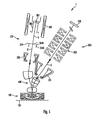
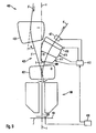
- FIG. 1 is a schematic diagram symbolically illustrating basic functions and components of an electron microscopy system 1.
- the electron microscopy system 1 is of a scanning electron microscope type (SEM) using a plurality of primary electron beamlets 3' for generating primary electron beam spots on a surface of an object to be inspected, which surface is arranged in an object plane 101 of an objective lens arrangement 100.
- SEM scanning electron microscope type
- the primary electrons incident on the object at the beam spots generate secondary electrons emanating from the surface of the object.
- the secondary electrons form secondary electron beamlets entering the objective lens arrangement 100.
- the electron microscopy system 1 provides a secondary electron beam path 4' for supplying the plurality of secondary electron beamlets to a detecting arrangement 200.
- Detecting arrangement 200 comprises a projecting lens arrangement 201, 202 for projecting the secondary electron beamlets 4' onto a surface plane of an electron sensitive detector 203.
- the detector 203 can be one or more selected from a solid state CCD or CMOS, a scintillator arrangement, a micro channel plate, an array of PIN diodes and others.
- the primary electron beamlets 3' are generated by a beamlet generating arrangement 300 comprising an electron source 301, a beam liner tube 302, a collimating lens 303, a multi-aperture plate arrangement 304 and a field lens 305.
- an electron source 301 is arranged on an optical axis of the system in a beam liner tube 302 and is additionally immersed in a magnetic field generated by collimating lens 303.
- the electrons are extracted from the electron source 301 and form a diverging electron beam, which is collimated by collimating lens 303 to form a beam 3 for illuminating multi-aperture arrangement 304.
- Multi-aperture arrangement 304 comprises a multi-aperture plate 304A, which is mounted in a center of a cup-shaped electrode 304B.
- An electrical field may be generated between the cup-shaped electrode 304B and a flange at the end of beam liner tube 302, which may be a decelerating or retarding field, for instance.
- the multi-aperture arrangement forms a plurality of primary electron beamlets 3' from the single illuminating beam 3 impinging on the multi-aperture plate 304A. Details of multi-aperture arrangements may be found in the references cited in the introduction or WO 2005/024881 A2 ( U.S. provisional application serial no. 60/500,256 ) to the same Assignee, for instance.
- a field lens 305 and objective lens arrangement 100 are provided in the beam path 3' of the plurality of primary electron beamlets to project an image of a focus plane of the multi-aperture arrangement 304 onto object plane 101 to form an array of primary electron beam spots on the object.
- a beam path splitting/combining arrangement 400 is also provided in the primary electron beam path 3' in between the beamlet generating arrangement 300 and objective lens arrangement 100 and in the secondary electron beam path 4' in between the objective lens arrangement 100 and the detecting arrangement 200.
- Beam splitting arrangement 400 allows the beam paths of the primary electron beamlets 3' and the secondary electron beamlets 4' which both pass through the objective lens arrangement 100 to be separated such that the secondary electron beamlets are directed towards the detecting arrangement 200.
- An exemplary beam splitting arrangement will be described in more detail with reference to Figure 9 .
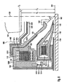
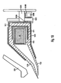
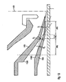
- Figure 2 shows a schematic cross section of a side view of an exemplary embodiment of an objective lens arrangement 100 which may be used in the electron microscopy system shown in Figure 1 .
- the objective lens arrangement 100 comprises an object mount 121 for mounting an object 7 to be inspected such that a surface of the object 7 is disposed within the object plane 101 of the electron microscopy system 1.
- the object 7 may be a semiconductor wafer, for instance, which is to be inspected for defects.
- the objective lens 102 comprises a first pole piece 123, which is concentric about the optical axis 120 (or axis of symmetry) of the objective lens 102 and has a radial inner end 124.
- a second magnetic pole piece 125 which is also rotationally symmetric and concentric about the optical axis 120 has a radial inner end 126 and is disposed at a distance from radial inner end 124 of the first pole piece 123 such that a substantially axial gap is formed between the radial inner ends 124 and 126.
- An excitation coil 129 is disposed radially outwardly of (i.e. at a greater distance from) the gap formed between inner ends 124, 126 in between the first and second pole pieces 123, 125.
- a yoke 130 forms part of the first pole piece and extends radially outwardly there from and is disposed opposite a yoke 131 formed by and extending radially outwardly from second pole piece 125.
- An electrically insulating resin 133 is provided in a gap between yoke 130, or excitation coil 129, respectively, which is disposed to be at least partially surrounded by yoke 130, and yoke 131 in that region where yokes 130, 131 are disposed adjacent to one another.
- Yoke 130 comprises a cylindrical portion 135, which is separated by insulating resin 133 from a corresponding adjacent cylindrical portion 136 of yoke 131, with the cylindrical portion 135 of the yoke 130 of the first pole piece 123 partially surrounding the cylindrical portion 136 of the yoke 131 of the second pole piece 125.
- the first yoke 130 further comprises an annular disc-shaped portion 137, which is separated by the insulating resin 133 from an adjacent corresponding annular disc-shaped portion 138 of yoke 131.
- first and second yokes 130, 131 are configured and arranged such that a region between yokes 130 and 131, or more precisely cylindrical and annular disc-shaped portions thereof, provides a considerable surface area such that a magnetic resistance between yokes 130 and 131 extending from and forming part of pole pieces 123 and 125, respectively, is low whilst both pole pieces 123, 125 are kept electrically insulated from each other.
- a power supply 141 is connected to first excitation coil 129 for supplying an excitation current to the first excitation coil 129 for generation of a magnetic field in the gap between radial inner ends 124, 126 of first and second pole pieces 123, 125.
- the electric field generated by the first excitation coil 129 induces a magnetic flux, indicated by arrows 142, in a magnetic circuit formed by magnetic pole pieces 123, 125 and yokes 130 and 131 such that the magnetic circuit is closed via the first gap formed between radial inner ends 124 and 126 of the first and second pole pieces 123 and 125, respectively.
- the magnetic field generated by the first excitation coil 129 has a focusing effect on the electrons of primary electron beamlets exiting from a beam tube 152 arranged coaxially with the optical axis 120.
- a lower end of the beam tube 152 is disposed in a region of the first gap between radial inner ends 124, 126 of the first and second pole pieces 123, 125.
- a high voltage supply 153 is provided to maintain the beam tube 152 at a potential of about +30 kV, in this embodiment.
- a voltage supply 155 is connected to the object mount 121 via a connector 156 to supply an adjustable high voltage of about -29.7 to -28 kV to the object mount 121.
- the object 7 to be inspected is arranged to be in electrical contact with object mount 121 such that object 7, too, is maintained at the adjustable potential of about -29.7 to 28.0 kV.
- a cathode of an electrode arrangement (upstream, not depicted) is maintained at a voltage of from about -30 kV to about -45 kV such that the primary electrons have a kinetic energy of from about 60 to 90 keV when they travel through the beam tube 152.
- a lower end of beam tube 152 is disposed at a distance from the object plane 101 such that the primary electrons experience a decelerating electric field in a space between the lower end of the beam tube 152 and the object plane 101. The primary electrons will then be incident on the object 7 with a landing energy of from about 50 eV to about 3000 eV.
- a radial inner portion of the first pole piece 123 i.e. a portion comprising a radial inner part of yoke 130 and radial inner end 124 of the first pole piece 123, includes a cavity 124" in which an excitation coil 127 is disposed. Excitation coil 127 is connected to a non-depicted further power supply in a manner similar to power supply 141 and electrically insulated from the first pole piece 123 including yoke 130.
- a further gap 124' is formed within the radial inner end 124 of the first pole piece 123 which gap 124' is joined with cavity 124".
- the first pole piece is functionally divided and configured to form a fourth pole piece and a third gap 124'.
- excitation coil 127 When excitation coil 127 is excited by the respective power supply, a magnetic field is generated in a region of the gap 124', which magnetic field serves to finely adjust a strength and position of the focusing magnetic field generated by excitation coil 129 in the first gap between the first pole piece 123 and the second pole piece 125.
- the electrical field generated between the lower end of beam tube 152 and the object 7 is not only defined by their positions and voltages applied thereto, but is in the depicted embodiment also influenced by a voltage applied to the second pole piece 125.
- the radial inner end 126 of the second pole piece 125 may, for instance, be maintained at a voltage of +3.9 kV relative to the electrical connector 156 of object mount 121, by a high voltage source 159 which is coupled to both the electrical connector 156 and the second pole piece 125. An effect thereof is described in more detail with reference to Figure 5 below.
- shielding electrode 154 is shown to which the same voltage as to electrical connector 156 or object mount 121, respectively, is applied so as to shield the object from an electrical field in an area of the shielding electrode 154, thus preventing undesired charging of the object.
- the shielding electrode has an annular shape with an inner aperture, and is symmetric with respect to the optical axis 120 and further disposed such that charged particles may pass through the inner aperture to reach the object.
- a lower edge of second pole piece 125 is disposed, at its radial inner end 126, at a distance d 1 from the surface of object 7 which surface coincides with object plane 101.
- the lower end of beam tube 152 is disposed at a distance d 2 from the object plane 101.
- a diameter of the bore defined by radial inner end 126 of pole piece 125 is denoted D 1 and a diameter of the beam tube 152 at its lower end is denoted D 2 .
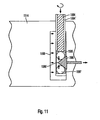
- FIG. 3 shows several field lines or equipotential lines representing the electrostatic field between the lower end of beam tube 152 and pole piece 125, and between pole piece 125 and the object 7.
- a field line 161 closest to the object plane 101 is a substantially straight line indicating a substantially homogeneous electrical field in a region around optical axis 120.
- Such a substantially homogeneous electrical field is generated for the purpose of decelerating each of the primary electron beamlets 3 to a desired landing energy.
- the substantially homogenous electrical field may also provide a extraction field for the secondary electrons emanating from the object 7 such that each of the secondary electron beamlets 4' has a substantially same kinetic energy when entering the objective lens 102.
- the electrical field at the object plane 101 may be divided into two components: A first component E 1 of the electrical field is generated by the potential difference between pole piece 125 and object 7, and a second component E 2 is generated by the potential difference between beam tube 152 and object 7. Both components have a substantially same effect on the electrical field at the object plane 101 in a region around the optical axis 120. This may be illustrated by changing the voltages applied to the beam tube 152 and to the pole piece 125 according to the following two settings: in a first setting, beam tube 152 is set to a potential of 59 kV relative to the object 7, and pole piece 125 is at the same potential as the object 7.
- the resulting electrical field at the object plane 101 and on the optical axis 120 is 1.8 kV/mm.
- pole piece 125 is at a potential of 3.9 kV relative to the object 7 and the beam tube 152, and the resulting electrical field at the object plane 101 is 1.2 kV/mm.
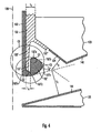
- a third pole piece 163 extends almost parallel to the object plane and has a radial inner end 164.
- the radial inner end 164 of the third pole piece 163 is disposed at a greater distance from the optical axis 120 than the radial inner end 126 of the second pole piece 125, and both radial inner ends are disposed in a same plane orthogonal to the optical axis 120.
- a radial gap is thus formed between radial inner end 164 of third pole piece 163 and radial inner end 126 of second pole piece 125.
- Pole piece 163 is integrally formed with yoke 131 such that a magnetic circuit is formed by pole piece 125, yoke 131 and pole piece 163, with this magnetic circuit being closed via the gap formed between inner ends 126 and 164 of pole pieces 125 and 163, respectively.
- a magnetic flux, indicated by arrows 166, in this magnetic circuit is generated by an excitation coil 167 to which current is supplied by a power supply 169.
- a space formed in the gap between pole pieces 125 and 163 is filled with an insulating resin 170 which serves to form a layer of insulating material between excitation coil 167 and pole pieces 125 and 163 and yoke 131.
- the excitation coil 167 is electrically insulated from pole pieces 125 and 163 such that it may be operated at ground potential.
- the third pole piece 163 has a radial inner annular portion 1631P where a surface of the third pole piece facing the object 7 extends substantially parallel to the object 7 disposed in the object plane at a first distance from the object 7.
- the third pole piece 163 has a radial outer annular portion 163OP where the surface of the third pole piece 163 facing the object 7 extends substantially parallel to the object plane 101 at a second distance from the object 7. The second distance is greater than the first distance, that is the outer annular portion 163OP is disposed further away from the object 7 than the inner annular portion 163IP.
- first and second distances may refer to average first and second distances.
- Inner and outer annular portions 163IP, 163OP are joined by middle portion 163MP, which is disposed at a greater angle relative to the object 7 than both the inner and outer annular portions 163IP, 163OP of the third pole piece 163. It can also be seen from Fig. 2 that a radial outer end of the inner annular portion of the third pole piece is disposed radially within the inner aperture of the shielding electrode.
- FIG. 2 further schematically indicates a supply line 171 of cooling water to provide cooling for excitation coil 167.
- the line 171 is supplied with cooling water by a cooling water supply 172, which is also set to ground potential.
- the cooling water supply 172 and the power supply 169 may be conveniently operated at ground potential as a result of electrical insulation being provided between excitation coil 167 and pole pieces 163 and 125.
- the power supply 169 is adjusted to supply an excitation current such that the magnetic field generated in the gap between inner ends 126 and 164 of pole pieces 125 and 163 compensates the focusing magnetic field, generated in the gap between inner ends 124 and 126 of pole pieces 123 and 125, in the object plane 101 and on the optical axis 120.
- the focusing field may be advantageously compensated to zero, which results in the electrons of the primary electron beamlets, which are incident on the object 7, experiencing substantially no magnetic field immediately above the object 7. This absence of magnetic field in said region allows improving telecentricity as well as errors resulting from an image rotation, which would be induced by the focusing magnetic field.
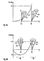
- Figure 5 shows graphs of magnetic flux density or magnetic field strength B and electrical field strength E along the optical axis 120.
- the magnetic field strength B steeply rises to a maximum at a position 181 on the optical axis 120 of the embodiment depicted in Figure 2 .
- the magnetic field B shows only a slow decrease with increasing further distance from object plane 101.
- Such a moderate decrease of B at an increasing distance from the object plane 101 may be achieved by a tapering shape of a bore formed by radial inner end 124 (the inner portion) of pole piece 123.
- the bore has a minimum diameter of about 20 mm.
- a front surface portion of pole piece 123 which is closest to the object plane 101, is disposed at a distance of about 20 mm in a second plane 184, and a diameter of the bore at this portion is about 41 mm (front diameter).
- the diameter of the bore formed by the radial inner end 124 of pole piece 123 radially increases with decreasing distance from the object plane 101 from a minimum value of about 22 mm to a maximum value of about 41 mm (front diameter) in plane 184.
- This particular geometry of the radial inner end 124 (or inner portion) of pole piece 123 allows to achieve the relatively moderate decrease of focusing magnetic field strength B with increasing distance from the object plane 101.
- Figure 5 also indicates a ⁇ -ray, which represents a ray starting off at a distance from the optical axis 120 and parallel to the optical axis 120 in the focus plane of the objective lens.
- This ray ⁇ crosses the optical axis 120 at a position close to position 181, which is the location of the maximum of the focusing magnetic field strength B. This results in a low value of the field curvature, for instance.
- Figure 5 further illustrates that ray ⁇ intersects the object plane 101 at an angle with respect to the optical axis. This indicates that a linear telecentric error may be present in the optical system. However, the small linear telecentric error is not only tolerated but purposely chosen such that a third order telecentric error is reduced, as illustrated with reference to Figures 6a and 6b below.
- Figure 6a illustrates a dependency of the third order telecentric error which objective lens 102 would provide if no first order telecentric error was present.
- An average angle of incidence ⁇ and thus the third order telecentric error increases with increasing distance r from the central axis or optical axis 120, respectively, according to r 3 .
- cones 191 indicate focused beams of primary electrons incident on object plane 101 at locations 192.
- Directions 193 indicate average directions of incidence of the primary electrons of these focused beams at the respective locations 192. These average directions 193 are oriented under average angles of incidence ⁇ with respect to the optical axis.
- a maximum average angle ⁇ at a maximum distance of a primary electron beam 191 from the optical axis 120 may be as much as 40 mrad.
- the field lens 305 shown in Figure 1 may be designed such that it introduces a linear telecentric error such that the beam path entering objective lens arrangement 100 is not a telecentric beam path.
- This results in a dependency of the third order telecentric error as shown in Figure 6b : starting from r 0, the average angle of incidence ⁇ will first pass through a minimum of -10 mrad and then reach a maximum of +10 mrad at the maximum value of r.
- a maximum value of the third order telecentric error has been successfully reduced.
- Figure 6b may be also interpreted as follows: in an inner ring portion 195 where the negative maximum ⁇ (r) is located, the electron beams incident on the object plane 101 are diverging from the optical axis (negative average angle of incidence, negative maximum ⁇ i ), and in an outer ring portion 196 surrounding inner ring portion 195, the primary electron beams incident on the object plane 101 are converging with respect to the optical axis (positive angle of incidence, maximum average angle of incidence ⁇ o ).
- This scenario may be suitably expressed by the ratio 0.5 ⁇ ⁇ i ⁇ 0 ⁇ 2.
- Line C S in Figure 5 further indicates the dependency of the field curvature, and line E' a dependency of the derivative of the electrical field strength E along the optical axis 120.
- Beam tube 152 is, for the largest part, a straight pipe having a substantially constant wall thickness down to a lower end.
- Lower end of beam tube 152 is constituted by a part of beam tube 152, which is turned by about 180° in a direction of a radial outer side of beam tube 152.
- the lower end is formed into a rounded rim, leaving a gap 152" between a radially outer side of the straight section of beam tube 152 and rounded rim 152'.
- Gap 152" has a substantially rectangular shape and extends parallel to the wall of the straight part of beam tube 152.
- a width t 4 i.e. a dimension in radial direction, of gap 152" is about 2mm.
- a cross-section of rim 152' may be suitably described by means of radii of circles fitted to an outer surface of rim 152', i.e. a surface facing away from the straight part of beam tube 152.
- the surface profile of rim 152' may be described by a radius of circle C1, which radius is about 1.2 mm, an adjacent part 152'b described by a radius of circle C4, which is about 11 mm, further adjacent part 152'c by a radius of circle C3, which radius is about 3 mm, a radially outer lower end 152'd of rim 152' by a radius of circle C5, which radius is about 6 mm, and a radially inner lower end 152'e of rim 152' by a radius of circle C2, which radius is about 1.2 mm.
- the uppermost part 152'a of rim 152' is spaced a distance t 2 of about 5mm apart from a radial inner end 124 of the first pole piece 123.
- the radially lower end 152'd of rim 152' is spaced a distance t 3 of about 10 mm apart from electrode 144 disposed on the second pole piece 125.
- This shape of the beam tube 152 in particular the design of rim 152' enables the realization of an advantageous shape of electrical field.
- a slanted and/or tapered area of inner end 124 of first pole piece 123 is efficiently separated from the optical axis 120.
- An insulating member 132 is disposed in a spacing formed in between a part of radial inner end 124 that extends in parallel to an outer side of beam tube 152 and the outer side of beam tube 152 and has a thickness or width t 1 of about 4mm in that area.
- insulating member 132 is split into two portions 132' and 132", with portion 132' extending further along a radial outer side of beam tube 152 until a lower end of gap 152" and portion 132" extending a short way along the slanted portion of the first pole piece 123.
- This shape and arrangement of insulating member 132 allows efficient electrical insulation of the first pole piece 123 as well as rim 152' from the pipe-shaped portion of beam tube.
- the region inside gap 152" is void of any electrical fields thus being advantageous for avoiding occurrences of creeping currents and surface leakages.
- a portion of the slanted (or tapered) portion of the first pole piece 123 is covered by electrode material 140.
- Figure 7 illustrates a further embodiment of the objective lens arrangement according to the present invention.
- the numbering of components of the objective lens arrangement of Figure 2 is adhered to.
- a shape of the first pole piece 123 is different from the embodiment depicted in Figure 2 in that is does not provide a cavity and thus no fourth pole piece, and thus no additional adjusting magnetic field is provided. Instead, alignment elements (not depicted) are disposed in a space 149 between upper radial inner end 124'" of the first pole piece 123 and insulation 132 of beam tube 152. Insulation 132 of beam tube 152 comprises several subsections 132', 132" that have been described in detail with reference to Figure 4 .
- a surface of the second magnetic pole piece 125 facing away from the object plane 101 is, in a radially inner area, covered by electrode material 144, which is connected to electrode material 144' disposed on a radially inner portion of a surface of the third pole piece 163 facing towards the object plane 101.
- An insulation between first pole piece 123 and second pole piece 125 is provided by insulating resin 133, which insulating resin 133 extends radially inwards up to a radially outer edge of electrode material 144.
- a space in which excitation coil 129 is disposed inside the first pole piece 123 is separated from an inside of the objective lens arrangement via insulating member 143, one end of which is attached to the first pole piece 123 by a screw 145, wherein a gasket 146 is provided in a gap adjacent to the screw in between the one end of the insulating member 143 and first pole piece 123.
- An additional gasket 146' is provided at the other end of insulating member 143, which end of the insulating member 143 is interposed between insulating resin 133 and the annular disc-shaped portion of the first pole piece 123.
- Water-cooling system 173 is disposed immediately adjacent to a side of excitation coil 129, which faces away from the object plane 101, which water cooling system 173 is attached via an electrically insulated screw 175 to yoke 130 of the first pole piece 123. Water-cooling system 173 is connected to a cooling water supply 174 disposed outside of objective lens arrangement 102. The water-cooling system is thus provided conveniently in an environment of about atmospheric pressure.
- Excitation coil 167 as well as a line of cooling water 171 are embedded in cast resin 170 in a spacing formed inside second and third pole pieces 125, 163 and yoke 131 to provide electrical insulation from the second and third pole pieces 125, 167 as well as allowing cooling water supply 172 to be provided in an environment of about atmospheric pressure.
- a gasket 147 is provided adjacent to a radial inner end of cast resin 170, which is also pressed against a surface of the second pole piece 125 facing towards the object plane 101 and a surface of the third pole piece 163 facing away from the object plane 101, thus providing a pressure seal.
- the above-described insulating arrangements are advantageous in that they dispose of the need to evacuate large spacings inside the objective lens arrangement.
- a ceramic/cast resin member 134 is provided between shielding electrode 154 and a surface of the third pole piece 163 facing towards the object plane 101 in order to provide both electrical insulation between the third pole piece 163 and the shielding electrode 154 as well as to provide a pressure seal.
- a radially inner end of cast resin/ceramic member 134 has a portion of decreased thickness to accommodate a gasket 148 in between the thin portion of resin/ceramic member 134 and the object-facing surface of the third pole piece 163.
- Cast resin/ceramic member 134 and shielding electrode 154 are attached to connecting ring 180', which connects the shielding electrode to a further ring 180, disposed in alignment with shielding electrode 154.
- the further ring 180 has a ring 139 of ceramic/resin material disposed thereon, which, in turn, is connected to cast resin/ceramic member 134 and yoke 130 via screw 179, connecting member 178, and connecting member 177, which is attached to yoke 130 via screw 176.
- FIG 8 a further embodiment of the objective lens arrangement according to the present invention is illustrated.
- the principal layout of the main components, such as pole pieces and beam tube, corresponds largely to that of the previously described embodiments.
- a main difference between the embodiments of Figures 2 and 7 on the one hand and Figure 8 on the other hand is given by the arrangement of the first pole piece relative to the beam tube.
- the first pole piece 123 was electrically insulated from the beam tube 152 and at ground potential
- an inner portion of the first pole piece 1501 is electrically connected to beam tube 1152.
- the beam tube 1152 is attached to a radial innermost portion of the first pole piece 1501.
- This configuration has an advantage in that provision of voltage to the beam tube 1152 is facilitated as compared to the previously described embodiments.
- the first pole piece is hence, in this embodiment, set to the same potential as the beam tube. This has no detrimental effect on an electrostatic field or magnetic field in the region of the beam tube 1152.
- the first pole piece being set to a voltage necessitates the division of the first pole piece into an inner portion 1501 which is connected to the beam tube 1152 and electrically insulated from a second portion 1502 of the first pole piece by an insulating layer 1503.
- the inner portion 1501 comprises a cylindrical portion 1501A which is arranged to face and be arranged in parallel to a cylindrical portion 1502A of the outer portion 1502 of the first pole piece. Additionally, the inner portion 1501 of the first pole piece comprises a flat, annular section 1501B joined in a radially outwards direction to the cylindrical portion 1501A and being arranged parallel and opposite to an annular section 1502B of the outer portion of the second pole piece, such as to enable a closed magnetic circuit. Insulating layer 1503 extends along a section of tapering inner portion of the first pole piece 1501, and fills a gap formed between cylindrical portions 1501A, 1502B as well as annular portions 1501B, 1502B.
- the inner portion 1501 of the first pole piece also comprises a conus-shaped section having a conus opening angle ⁇ with respect to the optical axis 1120.
- water-cooling lines 1173 disposed around excitation coil 1129 are also illustrated in Figure 8 .
- a further difference to the previously described embodiments lies in the mounting of the second and third pole pieces, the cooling of the excitation coil arranged in between the second and third pole pieces, and the sealing of spaces inside the various components.
- Excitation coil 1167 is encased on three sides in ceramic insulting material 1510, with both the excitation coil 1167 as well as the ceramic insulating material 1510 being fixed in the space between the second and third pole pieces by cast resin 1511.
- the ceramic insulating material 1510 is connected to an outer ring of thermally conductive material, which in turn, is connected to the first pole piece via copper wiring. This arrangement is not depicted in Figure 8 , for simplicity's sake, but described in detail with reference to Figure 10 .
- Figure 8 shows a part of the mounting structure for holding the second and third pole pieces 1163, 1125.
- the mounting structure comprises a holding bracket 1512 disposed on a radially outer side of the second and third pole pieces 1163, 1125, which bracket 1512 spans an upper side of the second pole piece 1125 and a lower side of the third pole piece 1163.
- a further insulating layer 1513 is provided, which extends further along the pole pieces 1163, 1125.
- the bracket 1512 is fixed to a mounting ring 1514.
- Mounting ring 1514 is held in position by three metal wires 1515 which are fixed to a lower portion of the first pole piece via connecting member 1516. This mounting structure allows adjusting a position of the pole pieces 1125, 1163 with respect to the first pole piece and the object plane.
- this mounting structure enables the second and third pole pieces 1125, 1163 to be disposed entirely in a vacuum environment thus eliminating the need to evacuate a space inside the two pole pieces 1125, 1163 and eliminating a plurality of seals thus increasing an ease of operation and installation.
- the shape chosen for the inner portion 1501 of the first pole piece allows to integrate a component disposed upstream of the objective lens arrangement within a space or bore formed by the inner portion 1501, thus decreasing an overall space requirement of an inspection system and improving optical properties of the system.
- a lower part of a beam path splitting arrangement 1400 is depicted, with an outside thereof being shown in a schematic and simplified manner as outline 1400'.
- a lower portion of a magnetic field arrangement 1407 is shown.
- a step-shaped protrusion 1501C is formed on an inside of the inner portion of the first pole piece 1501, which inside faces away from the object plane.
- a holding element 1575 having an upper side with an insulating layer 1576 attached thereto is held by and fixed to protrusion 1501C of the inner portion 1501 of the first pole piece.
- the outside 1400' of the beam path splitting arrangement may be advantageously formed such that its outline corresponds to that formed by the holding elements 1575 and the insulating layer 1576 thereon.
- the lower portion of the beam path splitting arrangement 1400 may then be arranged such that it remains spaced apart from the holding element 1575 or alternatively such that it rests on holding element 1575 (or insulating layer 1576, respectively).
- the lower portion of beam path splitting arrangement 1400 is inserted into a space formed by the cylindrical portion 1501A and annular portion 1501B of the first pole piece.
- a lower end of the beam path splitting arrangement and in particular a lower end P1 of the magnetic field arrangement 1407, is disposed at a first distance D 1 from the object plane 1101 which first distance D 1 is smaller than a second distance D 2 between an upper side P2 of the excitation coil 1129 and the object plane 1101.
- a conical shaped inner lower portion and a cylindrical upper portion of the inner portion of the first pole piece thus accommodate a portion of the beam splitting arrangement.
- FIG 9 a schematic illustration of an exemplary beam path splitting arrangement 400 and a simplified embodiment of objective lens arrangement 100 is given.
- Primary electron beam path 3' comprising a plurality of primary electron beamlets enters a first magnetic field portion 403 of beam path splitting arrangement 400.
- Field portion 403 provides a homogeneous magnetic field deflecting the primary electron beam path by an angle ⁇ to one side, in particular to the left in a direction of travel of the electrons, as viewed in Figure 9 .
- the primary electron beam path 3' subsequently passes a drift region 405 which is substantially free of magnetic fields such that the primary electron beam path 3' follows a straight line in drift region 405.
- the primary electron beam path 3' enters a field region 407 in which a homogeneous magnetic field is provided for deflecting the primary electron beam path 13 at an angle ⁇ to the right.
- primary electron beam path 3' enters the objective lens arrangement 100 which serves to focus the primary electron beamlets onto the surface of object 7 positioned in object plane 101.
- the axis 120 of the objective lens arrangement 100 coincides with optical axis z of the entire system.
- the objective lens arrangement 100 comprises a magnetic lens group having a magnetic focusing function and an electrostatic lens group having an electrostatic focusing function on the primary electron beamlets. Possible configurations of this electrostatic lens group according to the present invention have been described before, with reference to Figures 2 and 8 , for instance. Further, the electrostatic lens may be configured to exert a decelerating effect on the primary electrons by an electrical field for decelerating the primary electrons before impinging on object surface 7.
- the electrostatic lens arrangement referred to in the context of the description of this Figure may be chosen from any suitable embodiments as described above.
- a controller 420 is provided for changing the voltage supplied to the electrostatic lens arrangement such that the kinetic energy with which the primary electrons impinge onto the object, the landing energy, may be adjusted, for instance in a range of about 0,3 keV to 2,0 keV.
- the kinetic energy with which the primary electrons pass the beam path splitting arrangement 400 is generally constant and independent of the landing energy of the primary electrons on the object surface.
- the absolute values of the field strengths in field portions 403 and 407 are about equal, and lengths of field portions 403 and 407 are chosen such that a spatial dispersion induced by the deflection by the angle ⁇ to the left and the subsequent deflection by the angle ⁇ to the right is substantially zero. Further, the field portions 403 and 407 and the drift region 405 are chosen such that the deflections induced by the beam path splitting arrangement 400 on the primary electron beam path 3' are in first order substantially stigmatic and in first order substantially distortion free. Thus, a pattern may be imaged in high quality onto the surface of object 7. This imaging quality is maintained substantially independent of the landing energy of the primary electrons onto the object 7.
- the secondary electron beam path 4' comprising a plurality of secondary electron beamlets is separated from the primary electron beam path 3' by field region 407 which deflects the secondary electron beam path 4' by an angle ⁇ to the right.
- the secondary electrons emanating from the object 7 with a kinetic energy range of about 0 eV to 100 eV, for instance, will be accelerated by the electrical field generated by electrostatic lens arrangement of the objective lens arrangement 100 to a kinetic energy which is dependent on a setting provided by controller 420 for adjusting the landing energy of the primary electrons.
- the kinetic energy of the secondary electrons entering field region 407 will change in dependence of the landing energy of the primary electrons.
- Deflection angle ⁇ for the secondary electron beam path 4' provided by field region 407 will change, accordingly.
- the secondary electron beam path passes a drift region 409 which is substantially free of magnetic fields before entering a further magnetic field region 411 providing a homogeneous magnetic field deflecting the secondary electron beam path 4' further to the right.
- Field strength of field region 411 may be adjusted by a controller 413.
- the secondary electron beam path immediately enters a further field region 415 providing a homogeneous magnetic field, a field strength of which may be also adjusted by controller 413.
- Controller 413 operates in dependence of a setting of the landing energy of primary electron beams and adjusts the magnetic field strength in field regions 411 and 415 such that the primary electron beam path leaves field region 415 at a pre-defined position and in a pre-defined direction which are independent of the landing energy of the primary electrons and the deflection angle ⁇ , respectively.
- the two field regions 411, 415 perform a function of two subsequent beam deflectors which allows to adjust the secondary electron beam to coincide with the pre-defined secondary electron beam path 4' when the same leaves magnetic field region 415.
- the changes in the magnetic field strengths of field regions 411, 415 caused by controller 413 result in changes of a quadrupole effect, which these electron optical elements 411, 415 have on the secondary electrons.
- a further magnetic field region 419 is provided immediately downstream of field region 415.
- a homogeneous magnetic field is provided, a field strength of which is controlled by controller 413.
- a quadrupole lens 421 is provided downstream of magnetic field region 419 which is controlled by controller 413 to compensate, in cooperation with magnetic field region 419, the remaining quadrupole effect induced by field portions 411, 415 when compensating the beam path for different landing energies of the primary electrons.
- the electron-optical components 407, 409, 411, 415, 419 and 421 provided in the secondary electron beam path are configured such that, for one particular setting of the landing energy of the primary electrons, the secondary electron beam path through the beam path splitting arrangement 400 is in first order substantially stigmatic, in first order distortion free, and in first order dispersion corrected. For other settings of the landing energy than 2 kV this imaging quality may be maintained, a reduction of the dispersion correction to a limited amount occurs, however.
- an intermediate image of object plane 101 is formed in a region of field portions 407, 411, 415 and 419.
- a position of the intermediate image will change along the beam axis in dependence of the setting of the landing energy of the primary electrons and the kinetic energy of the secondary electrons, accordingly.
- Excitation coil 1167 is, in this exemplary embodiment, surrounded on practically all sides by a ceramic, electrically insulating layer 1510. Both the excitation coil 1167 and the insulating layer 1510 extend substantially continuously in a full circle around the optical axis (with the exception of electrical connections of the excitation coil penetrating through the ceramic insulation which are connected to an external power supply, not shown).
- a further layer 1511 of electrically insulating material, in this instance cast resin, is provided on three sides of the arrangement of the excitation coil 1167 and ceramic insulation 1510.
- the ceramic insulation 1510 is connected via connecting members 1510A to an outer ring comprising both a ring of ceramic material 1512 and a ring comprising an outer ceramic sheath 1510B encasing an inner core 1510C made of copper. Both rings are fixed to mounting ring 1514, which is fixedly attached to the second and third pole pieces 1125, 1163 and has been described with reference to Figure 8 .
- the ceramic connecting member 1510A provides a thermally conductive contact between the ceramic insulation 1510 around the excitation coil 1167 and the copper core ring 1510C and the ceramic ring 1512 for removing heat generated by the excitation coil 1167.
- the connecting member 1510A is not formed as a continuous ring, but is formed of small ring sections disposed around a circumference of the yoke integrally formed with and connecting the second and third pole pieces 1125, 1163, which small sections penetrate through a radial outer side of the second and third pole pieces 1125, 1163 of said yoke.
- the copper and ceramic rings, 1510 A through C are connected via a (non-depicted) copper wire to a cooling system outside the evacuated inside of the objective lens arrangement.
- connection may be configured, for instance, in analogy to wire 1515 and connecting piece 1516 shown in Figure 8 in connection with the mounting structure and further extend through the first pole piece to connect to a cooling system of the excitation coil accommodated within the first pole piece.
- a cooling system is provided which facilitates electrical insulation of the cooling system from the excitation coil and also allows for a flexible mounting structure for the second and third pole pieces.
- FIG 11 an adjusting arrangement for adjusting a radial position of the second and third pole pieces, which are held by mounting ring 1514, as shown in Figure 8 , is illustrated in a schematic and simplified manner.
- An adjustment screw 1594 is accommodated in a bore 1594' of the mounting ring 1514.
- the lower end of the bore 1594' and thus the lower end of the screw 1594 are operably linked to a top of a chamber 1595 which contains two balls 1597 on top of one another, i.e. an upper and a lower ball, and a wedge-shaped member 1596, with a pointed edge 1596' of the wedge-shaped member 1596 being disposed in between the two balls 1597.
- This arrangement may further comprise a counter-bearing, which is only indicated in terms of its effect as arrows 1598 in Figure 11 .
- the top of chamber 1595 and the screw 1594 are further connected such that turning of the screw 1594 does not only drive the screw 1594 further into the mounting ring 1514 and into the chamber 1595 but also lifts up the mounting ring 1514 together with the bottom of the chamber such that, upon turning of the screw 1594, not only the upper ball is pushed downwards, but also the lower ball pushed upwards.
- the two balls are pushed further together, they both exert a force onto the wedge-shaped member 1596 such that the wedge-shaped member 1596 is moved in a radial direction.
- the embodiment schematically shown in Figure 12 largely corresponds to that shown in Figure 8 , the difference being that the embodiment shown in Figure 12 comprises a heating system.
- the depicted heating system comprises a heating coil 1199 which is provided inside the second excitation coil 1167.
- the heating coil 1199 comprises several windings of a wire, which is made from the same material as the wire of the second excitation coil 1167 and is disposed adjacent to the wire forming the secondary excitation coil 1167.
- the heating coil 1199 is connected to a power supply PS and controlled by a control unit C1 which adjusts a current supplied by the power supply PS to the heating coil 1199 in dependence of a temperature of the second and third pole pieces 1163, 1125 and an excitation current supplied to the second excitation coil 1167.
- the temperature of the second and third pole pieces 1163, 1125 is measured by temperature sensors T1 and T2, which supply the data of the measured temperatures to a control unit C2.
- the excitation current supplied to the second excitation coil 1167 is controlled by control unit C3.
- Control units C2 and C3 supply the data of the temperatures of the second and third pole pieces 1163, 1125 and of the excitation current supplied to the second excitation coil 1167 to control unit C1 of the heating system, which calculates an excitation current to be provided to the heating coil 1199 on the basis of the supplied data.
- Control units C1, C2, C3 may also be portions of a single control unit.
- the pole pieces and an environment on the inside of the objective lens arrangement may be kept at a constant temperature and maintain a constant environment.
- FIG 13 a detail of the embodiment shown in Figure 8 is shown to illustrate angles formed between inside surfaces of the second and third pole pieces 1163, 1125.
- the second pole piece 1125 has a surface 1125S facing the third pole piece 1163 and the third pole piece 1163 has a surface 1163S facing the second pole piece 1125.
- the surfaces 1125S, 1163S of the second and third pole pieces 1125, 1163 form an angle ⁇ 1 between them which is about 9°.
- IPR2 in Fig.
- the surfaces 1125S, 1163S of the second and third pole pieces 1125, 1163 form an angle ⁇ 2 between them which is about 10°.
- the surfaces 1125S, 1163S of the second and third pole pieces 1125, 1163 form an angle ⁇ 3 between them which is about 15°.
- Combination 1 An objective lens arrangement comprising:
- Combination 2 The objective lens arrangement according to Combination 1, wherein the first power supply is configured to generate the excitation currents such that a magnetic field in a region on the object plane and about the axis of symmetry is substantially zero.
- Combination 3 The objective lens arrangement according to Combination 1 or 2, further comprising:
- Combination 4 The objective lens arrangement according to one of Combinations 1 to 3, wherein the second and third pole pieces are electrically connected with each other and wherein the first pole piece is electrically insulated from the second and third pole pieces by an insulating layer.
- Combination 5 The objective lens arrangement according to Combination 4, wherein the insulating layer is provided between an outer cylindrical portion integrally formed with the first pole piece and a yoke formed by the second and third pole pieces.
- Combination 6 The objective lens arrangement according to Combinations 4 or 5, wherein the insulating layer is provided between an outer annular disc shaped portion integrally formed with the first pole piece, and an outer portion of the second pole piece.
- Combination 7 The objective lens arrangement according to Combination 4, wherein the first pole piece comprises an inner member and an outer member with the inner and outer members being electrically insulated from one another by an insulating layer.
- Combination 8 The objective lens arrangement according to Combination 7, wherein the insulating layer is provided between the outer member of the first pole piece and an outer portion of the second pole piece.
- Combination 9 The objective lens arrangement according to Combination 7 or 8, wherein the outer member of the first pole piece is configured to accommodate the first excitation coil and wherein the inner member of the first pole piece comprises a substantially conical portion extending towards the axis of symmetry.
- Combination 10 The objective lens arrangement according to Combination 7, wherein the outer member has a substantially annular shape.
- Combination 11 The objective lens arrangement according to one of Combinations 1 to 10 wherein the first gap is a substantially axial gap and the second gap is a substantially radial gap.
- Combination 12 The objective lens arrangement according to Combination 11, wherein the radial inner end of the third pole piece and the radial inner end of the second pole piece are disposed in substantially a same plane extending substantially parallel to the object plane.
- Combination 13 The objective lens arrangement according to Combination 11 or 12, wherein the radial inner end of the third pole piece and the radial inner end of the second pole piece are disposed closer to the object plane than the radial inner end of the first pole piece.
- Combination 14 The objective lens arrangement according to one of Combinations 1 to 13, further comprising a heating system disposed within at least one of the first and second excitation coil, the heating system comprising a heating coils disposed in the vicinity of the at least one of the first and second excitation coils and a control portion for controlling and adjusting a current passing through the heating coil.
- Combination 15 The objective lens arrangement according to Combination 14, wherein the control portion is configured to adjust the current passing through the heating coil in dependence of at least one of a current passing through the at least one of the first and second excitation coils, a temperature of the third pole piece and a temperature of the second pole piece.
- Combination 16 An objective lens arrangement, comprising:
- Combination 17 The objective lens arrangement according to Combination 16, further comprising a third voltage source for supplying a voltage to the second pole piece such that a potential of the second pole piece is from about 0.1 kV to about 10 kV above a potential of the electrical connector.
- Combination 18 An objective lens arrangement according to Combination 17, wherein the third voltage source is an adjustable voltage source.
- Combination 19 An objective lens arrangement according to one of Combinations 16 to 18, wherein the beam tube is electrically insulated from the first pole piece.
- Combination 20 The objective lens arrangement according to Combination 19, wherein the first pole piece is set substantially at ground potential.
- Combination 21 The objective lens arrangement according to Combination 17, wherein the third voltage source is connected to the electrical connector and the second pole piece.
- Combination 22 The objective lens arrangement according to Combination 17, further comprising a third pole piece having a radial inner end which is disposed at a distance from the radial inner end of the second pole piece to form a second gap, wherein the first pole piece is electrically insulated from the second and third pole pieces by an insulating layer.
- Combination 23 The objective lens arrangement according to Combination 22, wherein the insulating layer is provided between an outer portion of the first pole piece and an outer portion of the second pole piece.
- Combination 24 The objective lens arrangement according to Combination 23, wherein the first pole piece comprises an inner member and an outer member, the outer member comprising the outer portion, with the inner and outer members being electrically insulated from each other by an insulating layer.
- Combination 25 The objective lens arrangement according to Combination 24, wherein the outer member of the first pole piece is configured to accommodate the first excitation coil and wherein the inner member of the first pole piece comprises a substantially conical portion extending towards the axis of symmetry.
- Combination 26 The objective lens arrangement according to Combination 24 or 25, wherein the inner member of the first pole piece is disposed adjacent to the beam tube and electrically connected thereto.
- Combination 27 An objective lens arrangement, comprising:
- Combination 28 The objective lens arrangement according to Combination 27, further comprising: a first pole piece, wherein the first pole piece is substantially rotationally symmetric with respect to the axis of symmetry, wherein the first pole piece is disposed on the same side of the object plane of the objective lens arrangement as the second and third pole pieces, wherein a radial inner end of the first pole piece is disposed at a distance from the radial inner end of the second pole piece to form a first gap, and wherein the first pole piece is electrically insulated from the second and third pole pieces, wherein the third voltage source is further configured to supply the voltage to the second pole piece such that the second pole piece is at a potential differing from a potential of the first pole piece by more than about 15 kV, in particular more than 20 kV, in particular more than 25 kV, and in particular more than 30 kV; and a first excitation coil for generating a magnetic field in the first gap.
- Combination 29 The objective lens arrangement according to Combination 27 or 28, further comprising a cooling system having a cooling medium supply for supplying a cooling medium to the second excitation coil, wherein the cooling medium supply is substantially at ground potential.
- Combination 30 An objective lens arrangement, comprising:
- Combination 31 The objective lens arrangement according to Combination 30, further comprising:
- Combination 32 The objective lens arrangement according to Combination 30 or 31, further comprising a cooling system having a cooling medium supply for supplying a cooling medium to the second excitation coil.
- Combination 33 An objective lens arrangement, comprising:
- Combination 34 The objective lens arrangement according to Combination 33, wherein the shielding electrode is electrically connected to the electrical connector of the object mount.
- Combination 35 The objective lens arrangement according to Combination 33 or 34, wherein the shielding electrode has a substantially annular shape, wherein the axis of symmetry passes through an inner aperture formed by the annular shape.
- Combination 36 The objective lens arrangement according to one of Combinations 33 to 35, wherein the third pole piece has a surface opposite to the object mount, wherein the third pole piece has a radial inner annular portion in which the surface extends substantially parallel to the object plane at a first distance therefrom, wherein the third pole piece has a radial outer annular portion in which the surface extends substantially parallel to the object plane at a second distance therefrom, wherein the second distance is greater than the first distance, wherein the shielding electrode has an inner aperture and wherein a radial outer end of the inner annular portion of the third pole piece is disposed radially within the inner aperture of the shielding electrode.
- Combination 37 The objective lens arrangement according to Combination 36, wherein the radial outer annular portion is disposed at an angle of less than 30° with respect to the object plane.
- Combination 38 The objective lens arrangement according to Combination 36 or 37, wherein the radial inner annular portion is disposed at an angle of less than 20° with respect to the object plane.
- Combination 39 The objective lens arrangement according to one of Combinations 36 to 38, further comprising a second pole piece, wherein a radial inner end of the third pole piece and a radial inner end of the second pole piece form a gap between them, wherein the second pole piece has an inner angular portion with a surface facing the third pole piece and wherein the third pole piece has an angular portion with a surface facing the second pole piece, wherein the surfaces of the third and second pole pieces facing each other form an angle of less than 40°, in particular less than 35° between them.
- Combination 40 The objective lens arrangement according to Combination 39, wherein the gap is a substantially radial gap.
- Combination 41 The objective lens arrangement according to Combination 39 or 40, wherein the second pole piece has a radial inner portion wherein the surface facing the third pole piece is disposed at an angle of from between about 3° to about 35° with respect to the surface of the inner annular portion of the third pole piece facing the second pole piece.
- Combination 42 An objective lens arrangement, comprising:
- Combination 43 A charged particle beam system, comprising:
- Combination 44 The charged particle beam system according to Combination 43, wherein the following relation is fulfilled: 0.5 ⁇
- Combination 45 The charged particle beam system according to Combination 44, wherein
- Combination 46 The charged particle beam system according to Combination 45, wherein the location in the outer ring shaped portion where the average angle of incidence is the maximum average angle is disposed at a distance of more than 30 ⁇ m from the central axis.
- Combination 47 An objective lens arrangement, comprising:
- Combination 48 A particle optical inspection system, comprising an objective lens arrangement comprising:
- Combination 49 The particle optical inspection system according to Combination 48, wherein the inner portion of the first pole piece extends towards the axis of symmetry such that the radial inner end of the first pole piece is disposed closer to the object plane than a radial outer end of the inner portion of the first pole piece and wherein the lower end of the at least one magnetic lens is disposed within a space defined by the inner portion of the first pole piece.
- Combination 50 The particle-optical inspection system according to Combination 48, wherein the inner portion of the first pole piece has a substantially conical shape with the radial inner end being disposed closer to the object plane than a radial outer end and wherein the lower end of the at least one magnetic lens is disposed within the conus formed by the inner portion of the first pole piece.
- Combination 51 The particle optical inspection system according to Combination 50, the conus formed by the inner portion of the first pole piece having a conus opening angle in a range of from about 20° to about 70°.
Landscapes
- Chemical & Material Sciences (AREA)
- Analytical Chemistry (AREA)
- Physics & Mathematics (AREA)
- Electromagnetism (AREA)
- Electron Beam Exposure (AREA)
- Electric Connection Of Electric Components To Printed Circuits (AREA)
- Optical Recording Or Reproduction (AREA)
- Multi-Conductor Connections (AREA)
- Investigating Or Analyzing Materials By The Use Of Magnetic Means (AREA)
- Optical Head (AREA)
- Transition And Organic Metals Composition Catalysts For Addition Polymerization (AREA)
Claims (15)
- Objektivlinsenanordnung, umfassend:einen ersten Polschuh (125) und einen zweiten Polschuh (163), wobei die ersten und zweiten Polschuhe im Verhältnis zu einer Symmetrieachse (120) im Wesentlichen rotationssymmetrisch sind, wobei die ersten und zweiten Polschuhe auf einer gleichen Seite einer Objektebene (101) der Objektivlinsenanordnung angeordnet sind, wobei ein radiales inneres Ende des zweiten Polschuhs in einem Abstand von einem radialen inneren Ende des ersten Polschuhs angeordnet ist, um einen ersten Spalt zu bilden, wobei die ersten und zweiten Polschuhe elektrisch miteinander verbunden sind;eine erste Erregerspule (167), um in dem ersten Spalt ein Magnetfeld zu erzeugen; undeine erste Spannungsquelle (159), um den ersten Polschuh mit Spannung zu versorgen, so dass der erste Polschuh auf einem Potential liegt, das sich von einem Potential der ersten Erregerspule um mehr als 15 kV, insbesondere um mehr als 20 kV, insbesondere um mehr als 25 kV, insbesondere um mehr als 30 kV und insbesondere um mehr als 45 kV unterscheidet;wobei:(i) die Objektivlinsenanordnung ferner eine erste Energieversorgung (169) umfasst, um die erste Erregerspule mit einem Erregerstrom zu versorgen, wobei die erste Energieversorgung im Wesentlichen auf Massepotential liegt, und/oder(ii) die erste Erregerspule eine Vielzahl von Wicklungen aus einem isolierten Draht umfasst, und wobei mindestens eine weitere Isolierschicht (170) bereitgestellt wird, um die erste Erregerspule im Verhältnis zu mindestens einem der ersten und zweiten Polschuhe zu tragen.
- Objektivlinsenanordnung gemäß Anspruch 1, ferner umfassend:einen dritten Polschuh (123), wobei der dritte Polschuh zu der Symmetrieachse im Wesentlichen rotationssymmetrisch ist, wobei der dritte Polschuh auf der gleichen Seite der Objektebene der Objektivlinsenanordnung angeordnet ist wie die ersten und zweiten Polschuhe, wobei ein radiales inneres Ende des dritten Polschuhs in einem Abstand von dem radialen inneren Ende des ersten Polschuhs angeordnet ist, um einen zweiten Spalt zu bilden, wobei der dritte Polschuh von den ersten und zweiten Polschuhen elektrisch isoliert ist, wobei die erste Spannungsquelle ferner konfiguriert ist, um den ersten Polschuh mit der Spannung zu versorgen, so dass der erste Polschuh auf einem Potential liegt, das sich von einem Potential des dritten Polschuhs um mehr als 15 kV, insbesondere um mehr als 20 kV, insbesondere um mehr als 25 kV und insbesondere um mehr als 30 kV unterscheidet;und eine zweite Erregerspule (129), um in dem zweiten Spalt ein Magnetfeld zu erzeugen.
- Objektivlinsenanordnung gemäß Anspruch 2, wobei der dritte Polschuh von den ersten und zweiten Polschuhen durch eine Isolierschicht (133) elektrisch isoliert ist.
- Objektivlinsenanordnung gemäß Anspruch 3, wobei die Isolierschicht zwischen einem äußeren zylindrischen Abschnitt (135), der mit dem dritten Polschuh einstückig gebildet ist, und einem Joch, das durch die ersten und zweiten Polschuhe gebildet wird, bereitgestellt wird, und/oder wobei die Isolierschicht zwischen einem äußeren ringscheibenförmigen Abschnitt, der mit dem dritten Polschuh einstückig gebildet ist, und einem äußeren Abschnitt des ersten Polschuhs bereitgestellt wird.
- Objektivlinsenanordnung gemäß Anspruch 4, wobei der dritte Polschuh ein inneres Element und ein äußeres Element umfasst, wobei die inneren und äußeren Elemente durch eine Isolierschicht voneinander elektrisch isoliert sind, wobei die Isolierschicht zwischen dem äußeren Element des dritten Polschuhs und einem äußeren Abschnitt des ersten Polschuhs bereitgestellt werden kann, und wobei das äußere Element eine im Wesentlichen ringförmige Gestalt haben kann.
- Objektivlinsenanordnung gemäß Anspruch 5, wobei das äußere Element des dritten Polschuhs konfiguriert ist, um die zweite Erregerspule aufzunehmen, und wobei das innere Element des dritten Polschuhs einen im Wesentlichen konischen Abschnitt umfasst, der sich in Richtung auf die Symmetrieachse erstreckt.
- Objektivlinsenanordnung gemäß einem der Ansprüche 1 bis 6, ferner umfassend ein Kühlsystem (171, 172), das eine Kühlmittelversorgung aufweist, um die erste Erregerspule mit einem Kühlmittel zu versorgen, wobei die Kühlmittelversorgung insbesondere im Wesentlichen auf Massepotential liegt.
- Objektivlinsenanordnung gemäß einem der Ansprüche 1 bis 7, wobei der zweite Polschuh sich quer zur Symmetrieachse erstreckt, und wobei die Objektivlinsenanordnung ferner Folgendes umfasst:einen Objekthalter, um ein zu prozessuierendes Objekt in einer Objektebene zu halten, wobei der Objekthalter (121) einen elektrischen Verbinder (156) aufweist, um das Objekt mit einer elektrischen Spannung zu versorgen; undeine Abschirmelektrode (154), die von dem zweiten Polschuh elektrisch isoliert ist und zwischen dem zweiten Polschuh und dem Objekthalter angeordnet ist.
- Objektivlinsenanordnung gemäß Anspruch 8, wobei die Abschirmelektrode an den elektrischen Verbinder des Objekthalters elektrisch angeschlossen ist.
- Objektivlinsenanordnung gemäß Anspruch 8 oder 9, wobei die Abschirmelektrode im Wesentlichen ringförmig ist, wobei die Symmetrieachse durch eine Innenöffnung geht, die von der Ringform gebildet wird.
- Objektivlinsenanordnung gemäß einem der Ansprüche 8 bis 10, wobei der zweite Polschuh eine Oberfläche gegenüber dem Objekthalter aufweist, wobei der zweite Polschuh einen radialen inneren ringförmigen Abschnitt (163IP) aufweist, in dem sich die Oberfläche im Wesentlichen parallel zur Objektebene in einem ersten Abstand davon erstreckt, wobei der zweite Polschuh einen radialen äußeren ringförmigen Abschnitt (163OP) aufweist, in dem sich die Oberfläche im Wesentlichen parallel zur Objektebene in einem zweiten Abstand davon erstreckt, wobei der zweite Abstand größer ist als der erste Abstand, wobei die Abschirmelektrode eine innere Öffnung aufweist, und wobei ein radiales äußeres Ende des inneren ringförmigen Abschnitts des dritten Polschuhs radial innerhalb der inneren Öffnung der Abschirmelektrode angeordnet ist.
- Objektivlinsenanordnung gemäß Anspruch 11, wobei der radiale äußere ringförmige Abschnitt in einem Winkel von weniger als 30° im Verhältnis zur Objektebene angeordnet ist.
- Objektivlinsenanordnung gemäß Anspruch 11 oder 12, wobei der radiale innere ringförmige Abschnitt in einem Winkel von weniger als 20° im Verhältnis zu der Objektebene angeordnet ist.
- Objektivlinsenanordnung gemäß einem der Ansprüche 1 bis 13, wobei der erste Polschuh einen inneren Winkelabschnitt mit einer Oberfläche aufweist, die dem zweiten Polschuh zugewandt ist, und wobei das zweite Polschuh einen Winkelabschnitt mit einer Oberfläche aufweist, die dem ersten Polschuh zugewandt ist, wobei die Oberflächen der zweiten und ersten Polschuhe, die einander zugewandt sind, eine Winkel von weniger als 40°, insbesondere von weniger als 35° dazwischen bilden.
- Objektivlinsenanordnung gemäß einem der Ansprüche 1 bis 14, wobei der erste Polschuh einen radialen inneren Abschnitt aufweist, wobei die Oberfläche, die dem zweiten Polschuh zugewandt ist, in einem Winkel zwischen 3° bis 35° im Verhältnis zur Oberfläche des inneren ringförmigen Abschnitts des zweiten Polschuhs, das dem ersten Polschuh zugewandt ist, angeordnet ist.
Priority Applications (5)
| Application Number | Priority Date | Filing Date | Title |
|---|---|---|---|
| EP10012454A EP2270836B1 (de) | 2005-11-28 | 2006-11-28 | Teilchenoptische Komponente |
| EP10012424A EP2267754B1 (de) | 2005-11-28 | 2006-11-28 | Teilchenoptisches Inspektionssystem |
| EP10012397A EP2267753A3 (de) | 2005-11-28 | 2006-11-28 | Teilchenoptische Komponente |
| EP10012453A EP2270835B1 (de) | 2005-11-28 | 2006-11-28 | Teilchenoptische Komponente |
| EP10012425A EP2267755A3 (de) | 2005-11-28 | 2006-11-28 | Teilchenoptische Komponente |
Applications Claiming Priority (2)
| Application Number | Priority Date | Filing Date | Title |
|---|---|---|---|
| US74058105P | 2005-11-28 | 2005-11-28 | |
| EP06829160A EP1966815B1 (de) | 2005-11-28 | 2006-11-28 | Teilchenoptische komponente |
Related Parent Applications (1)
| Application Number | Title | Priority Date | Filing Date |
|---|---|---|---|
| EP06829160.8 Division | 2006-11-28 |
Related Child Applications (7)
| Application Number | Title | Priority Date | Filing Date |
|---|---|---|---|
| EP10012454A Division EP2270836B1 (de) | 2005-11-28 | 2006-11-28 | Teilchenoptische Komponente |
| EP10012453A Division EP2270835B1 (de) | 2005-11-28 | 2006-11-28 | Teilchenoptische Komponente |
| EP10012454.4 Division-Into | 2010-09-30 | ||
| EP10012425.4 Division-Into | 2010-09-30 | ||
| EP10012424.7 Division-Into | 2010-09-30 | ||
| EP10012397.5 Division-Into | 2010-09-30 | ||
| EP10012453.6 Division-Into | 2010-09-30 |
Publications (2)
| Publication Number | Publication Date |
|---|---|
| EP2211368A1 EP2211368A1 (de) | 2010-07-28 |
| EP2211368B1 true EP2211368B1 (de) | 2012-06-27 |
Family
ID=37728176
Family Applications (7)
| Application Number | Title | Priority Date | Filing Date |
|---|---|---|---|
| EP10012424A Active EP2267754B1 (de) | 2005-11-28 | 2006-11-28 | Teilchenoptisches Inspektionssystem |
| EP10012425A Withdrawn EP2267755A3 (de) | 2005-11-28 | 2006-11-28 | Teilchenoptische Komponente |
| EP06829160A Active EP1966815B1 (de) | 2005-11-28 | 2006-11-28 | Teilchenoptische komponente |
| EP10012453A Active EP2270835B1 (de) | 2005-11-28 | 2006-11-28 | Teilchenoptische Komponente |
| EP10012397A Withdrawn EP2267753A3 (de) | 2005-11-28 | 2006-11-28 | Teilchenoptische Komponente |
| EP10012454A Not-in-force EP2270836B1 (de) | 2005-11-28 | 2006-11-28 | Teilchenoptische Komponente |
| EP10003918A Active EP2211368B1 (de) | 2005-11-28 | 2006-11-28 | Teilchenoptische Komponente |
Family Applications Before (6)
| Application Number | Title | Priority Date | Filing Date |
|---|---|---|---|
| EP10012424A Active EP2267754B1 (de) | 2005-11-28 | 2006-11-28 | Teilchenoptisches Inspektionssystem |
| EP10012425A Withdrawn EP2267755A3 (de) | 2005-11-28 | 2006-11-28 | Teilchenoptische Komponente |
| EP06829160A Active EP1966815B1 (de) | 2005-11-28 | 2006-11-28 | Teilchenoptische komponente |
| EP10012453A Active EP2270835B1 (de) | 2005-11-28 | 2006-11-28 | Teilchenoptische Komponente |
| EP10012397A Withdrawn EP2267753A3 (de) | 2005-11-28 | 2006-11-28 | Teilchenoptische Komponente |
| EP10012454A Not-in-force EP2270836B1 (de) | 2005-11-28 | 2006-11-28 | Teilchenoptische Komponente |
Country Status (8)
| Country | Link |
|---|---|
| US (4) | US20090159810A1 (de) |
| EP (7) | EP2267754B1 (de) |
| JP (1) | JP5663722B2 (de) |
| KR (2) | KR101589306B1 (de) |
| CN (3) | CN102103966B (de) |
| AT (1) | ATE464647T1 (de) |
| DE (1) | DE602006013707D1 (de) |
| WO (1) | WO2007060017A2 (de) |
Families Citing this family (107)
| Publication number | Priority date | Publication date | Assignee | Title |
|---|---|---|---|---|
| JP5227643B2 (ja) * | 2008-04-14 | 2013-07-03 | 株式会社日立ハイテクノロジーズ | 高分解能でかつ高コントラストな観察が可能な電子線応用装置 |
| DE102008064696B4 (de) * | 2008-12-23 | 2022-01-27 | Carl Zeiss Microscopy Gmbh | Teilchenoptische Vorrichtung mit Magnetanordnung und ihre Verwendung zum Abbilden oder Beleuchten |
| US9336981B2 (en) | 2010-04-09 | 2016-05-10 | Applied Materials Israel Ltd. | Charged particle detection system and multi-beamlet inspection system |
| WO2012041464A1 (en) | 2010-09-28 | 2012-04-05 | Applied Materials Israel Ltd. | Particle-optical systems and arrangements and particle-optical components for such systems and arrangements |
| US8519353B2 (en) * | 2010-12-29 | 2013-08-27 | Varian Semiconductor Equipment Associates, Inc. | Method and apparatus for controlling an asymmetric electrostatic lens about a central ray trajectory of an ion beam |
| CN102148122B (zh) * | 2011-02-16 | 2012-07-18 | 北京航空航天大学 | 应用于透射电子显微镜的层叠式低像差会聚小透镜 |
| US8835866B2 (en) * | 2011-05-19 | 2014-09-16 | Fei Company | Method and structure for controlling magnetic field distributions in an ExB Wien filter |
| GB2497758A (en) * | 2011-12-20 | 2013-06-26 | Univ Antwerpen | Generation of charged particle vortex waves |
| EP2665082A1 (de) * | 2012-05-16 | 2013-11-20 | ICT Integrated Circuit Testing Gesellschaft für Halbleiterprüftechnik mbH | Element für schnelle Magnetstrahlablenkung |
| JP5667618B2 (ja) * | 2012-12-14 | 2015-02-12 | 株式会社アドバンテスト | 電磁レンズ及び電子ビーム露光装置 |
| JP6161430B2 (ja) * | 2013-06-25 | 2017-07-12 | 株式会社日立ハイテクノロジーズ | 電子レンズ及び荷電粒子線装置 |
| DE102013014976A1 (de) | 2013-09-09 | 2015-03-12 | Carl Zeiss Microscopy Gmbh | Teilchenoptisches System |
| DE102013016113B4 (de) | 2013-09-26 | 2018-11-29 | Carl Zeiss Microscopy Gmbh | Verfahren zum Detektieren von Elektronen, Elektronendetektor und Inspektionssystem |
| US9263233B2 (en) | 2013-09-29 | 2016-02-16 | Carl Zeiss Microscopy Gmbh | Charged particle multi-beam inspection system and method of operating the same |
| CN105765691B (zh) | 2013-09-30 | 2018-02-02 | 卡尔蔡司显微镜有限责任公司 | 带电粒子束系统和操作带电粒子束系统的方法 |
| US9966218B2 (en) * | 2014-04-28 | 2018-05-08 | Hitachi High-Technologies Corporation | Electron beam device |
| DE102014008083B9 (de) | 2014-05-30 | 2018-03-22 | Carl Zeiss Microscopy Gmbh | Teilchenstrahlsystem |
| DE102014008105B4 (de) | 2014-05-30 | 2021-11-11 | Carl Zeiss Multisem Gmbh | Mehrstrahl-Teilchenmikroskop |
| DE102014008383B9 (de) | 2014-06-06 | 2018-03-22 | Carl Zeiss Microscopy Gmbh | Teilchenstrahlsystem und Verfahren zum Betreiben einer Teilchenoptik |
| TWI502616B (zh) * | 2014-08-08 | 2015-10-01 | Nat Univ Tsing Hua | 桌上型電子顯微鏡以及其廣域可調式磁透鏡 |
| JP6204388B2 (ja) * | 2015-01-30 | 2017-09-27 | 松定プレシジョン株式会社 | 荷電粒子線装置及び走査電子顕微鏡 |
| JP6177817B2 (ja) * | 2015-01-30 | 2017-08-09 | 松定プレシジョン株式会社 | 荷電粒子線装置及び走査電子顕微鏡 |
| DE102015202172B4 (de) | 2015-02-06 | 2017-01-19 | Carl Zeiss Microscopy Gmbh | Teilchenstrahlsystem und Verfahren zur teilchenoptischen Untersuchung eines Objekts |
| US9691588B2 (en) | 2015-03-10 | 2017-06-27 | Hermes Microvision, Inc. | Apparatus of plural charged-particle beams |
| JP6718782B2 (ja) * | 2016-09-21 | 2020-07-08 | 日本電子株式会社 | 対物レンズおよび透過電子顕微鏡 |
| DE102016120902B4 (de) | 2016-11-02 | 2018-08-23 | Carl Zeiss Microscopy Gmbh | Vielstrahl-Teilchenmikroskop |
| JP6814282B2 (ja) | 2017-03-29 | 2021-01-13 | 株式会社日立ハイテク | 荷電粒子線装置 |
| CN111033676B (zh) | 2017-09-04 | 2022-08-30 | 株式会社日立高新技术 | 带电粒子线装置 |
| DE102018202428B3 (de) | 2018-02-16 | 2019-05-09 | Carl Zeiss Microscopy Gmbh | Vielstrahl-Teilchenmikroskop |
| DE102018202421B3 (de) | 2018-02-16 | 2019-07-11 | Carl Zeiss Microscopy Gmbh | Vielstrahl-Teilchenstrahlsystem |
| CN112055886A (zh) | 2018-02-27 | 2020-12-08 | 卡尔蔡司MultiSEM有限责任公司 | 带电粒子多束系统及方法 |
| US10811215B2 (en) | 2018-05-21 | 2020-10-20 | Carl Zeiss Multisem Gmbh | Charged particle beam system |
| DE102018115012A1 (de) | 2018-06-21 | 2019-12-24 | Carl Zeiss Microscopy Gmbh | Teilchenstrahlsystem |
| DE102018007455B4 (de) | 2018-09-21 | 2020-07-09 | Carl Zeiss Multisem Gmbh | Verfahren zum Detektorabgleich bei der Abbildung von Objekten mittels eines Mehrstrahl-Teilchenmikroskops, System sowie Computerprogrammprodukt |
| DE102018007652B4 (de) | 2018-09-27 | 2021-03-25 | Carl Zeiss Multisem Gmbh | Teilchenstrahl-System sowie Verfahren zur Stromregulierung von Einzel-Teilchenstrahlen |
| DE102018124044B3 (de) * | 2018-09-28 | 2020-02-06 | Carl Zeiss Microscopy Gmbh | Verfahren zum Betreiben eines Vielstrahl-Teilchenstrahlmikroskops und Vielstrahl-Teilchenstrahlsystem |
| DE102018124219A1 (de) | 2018-10-01 | 2020-04-02 | Carl Zeiss Microscopy Gmbh | Vielstrahl-Teilchenstrahlsystem und Verfahren zum Betreiben eines solchen |
| US11264198B2 (en) * | 2018-10-15 | 2022-03-01 | Applied Materials Israel Ltd. | Objective lens arrangement |
| DE102018133703B4 (de) | 2018-12-29 | 2020-08-06 | Carl Zeiss Multisem Gmbh | Vorrichtung zur Erzeugung einer Vielzahl von Teilchenstrahlen und Vielstrahl-Teilchenstrahlsysteme |
| TWI743626B (zh) | 2019-01-24 | 2021-10-21 | 德商卡爾蔡司多重掃描電子顯微鏡有限公司 | 包含多束粒子顯微鏡的系統、對3d樣本逐層成像之方法及電腦程式產品 |
| CN111477530B (zh) | 2019-01-24 | 2023-05-05 | 卡尔蔡司MultiSEM有限责任公司 | 利用多束粒子显微镜对3d样本成像的方法 |
| US10741355B1 (en) | 2019-02-04 | 2020-08-11 | Carl Zeiss Multisem Gmbh | Multi-beam charged particle system |
| DE102019004124B4 (de) | 2019-06-13 | 2024-03-21 | Carl Zeiss Multisem Gmbh | Teilchenstrahl-System zur azimutalen Ablenkung von Einzel-Teilchenstrahlen sowie seine Verwendung und Verfahren zur Azimut-Korrektur bei einem Teilchenstrahl-System |
| DE102019005364B3 (de) * | 2019-07-31 | 2020-10-08 | Carl Zeiss Multisem Gmbh | System-Kombination eines Teilchenstrahlsystem und eines lichtoptischen Systems mit kollinearer Strahlführung sowie Verwendung der System-Kombination |
| DE102019005362A1 (de) | 2019-07-31 | 2021-02-04 | Carl Zeiss Multisem Gmbh | Verfahren zum Betreiben eines Vielzahl-Teilchenstrahlsystems unter Veränderung der numerischen Apertur, zugehöriges Computerprogrammprodukt und Vielzahl-Teilchenstrahlsystem |
| DE102019008249B3 (de) | 2019-11-27 | 2020-11-19 | Carl Zeiss Multisem Gmbh | Teilchenstrahl-System mit einer Multistrahl-Ablenkeinrichtung und einem Strahlfänger, Verfahren zum Betreiben des Teilchenstrahl-Systems und zugehöriges Computerprogrammprodukt |
| KR102919104B1 (ko) | 2020-02-03 | 2026-01-29 | 아이엠에스 나노패브릭케이션 게엠베하 | 멀티―빔 라이터의 블러 변화 보정 |
| EP4100986A1 (de) | 2020-02-04 | 2022-12-14 | Carl Zeiss MultiSEM GmbH | Mehrstrahl-digitalabtastung und bilderfassung |
| EP3872837A1 (de) * | 2020-02-25 | 2021-09-01 | The Provost, Fellows, Scholars and other Members of Board of Trinity College Dublin | Polstück für ein elektronenmikroskop |
| JP7689139B2 (ja) | 2020-03-12 | 2025-06-05 | カール ツァイス マルティセム ゲゼルシヤフト ミット ベシュレンクテル ハフツング | マルチビーム発生ユニットおよびマルチビーム偏向ユニットの特定の改善 |
| DE102020107738B3 (de) | 2020-03-20 | 2021-01-14 | Carl Zeiss Multisem Gmbh | Teilchenstrahl-System mit einer Multipol-Linsen-Sequenz zur unabhängigen Fokussierung einer Vielzahl von Einzel-Teilchenstrahlen, seine Verwendung und zugehöriges Verfahren |
| DE102020115183B4 (de) | 2020-06-08 | 2026-01-29 | Carl Zeiss Multisem Gmbh | Teilchenstrahlsystem mit Multiquellensystem sowie Mehrstrahl-Teilchenmikroskop |
| DE102020121132B3 (de) | 2020-08-11 | 2021-09-23 | Carl Zeiss Multisem Gmbh | Verfahren zum Betreiben eines Vielzahl-Teilchenstrahlsystems mit einem Spiegel-Betriebsmodus und zugehöriges Computerprogrammprodukt |
| DE102020123567B4 (de) | 2020-09-09 | 2025-02-13 | Carl Zeiss Multisem Gmbh | Vielzahl-Teilchenstrahl-System mit Kontrast-Korrektur-Linsen-System |
| DE102021105201B4 (de) | 2021-03-04 | 2024-10-02 | Carl Zeiss Multisem Gmbh | Vielzahl-Teilchenstrahlmikroskop und zugehöriges Verfahren mit schnellem Autofokus mit speziellen Ausführungen |
| DE102020125534B3 (de) | 2020-09-30 | 2021-12-02 | Carl Zeiss Multisem Gmbh | Vielzahl-Teilchenstrahlmikroskop und zugehöriges Verfahren mit schnellem Autofokus um einen einstellbaren Arbeitsabstand |
| TW202220012A (zh) | 2020-09-30 | 2022-05-16 | 德商卡爾蔡司多重掃描電子顯微鏡有限公司 | 在可調工作距離附近具快速自動對焦之多重粒子束顯微鏡及相關方法 |
| DE102021200799B3 (de) | 2021-01-29 | 2022-03-31 | Carl Zeiss Multisem Gmbh | Verfahren mit verbesserter Fokuseinstellung unter Berücksichtigung eines Bildebenenkipps in einem Vielzahl-Teilchenstrahlmikroskop |
| DE102021112503B4 (de) * | 2021-05-12 | 2025-03-27 | Carl Zeiss Microscopy Gmbh | Teilchenstrahlvorrichtung mit einer Ablenkeinheit |
| TW202312205A (zh) | 2021-05-27 | 2023-03-16 | 德商卡爾蔡司多重掃描電子顯微鏡有限公司 | 多重射束帶電粒子系統與在多重射束帶電粒子系統中控制工作距離的方法 |
| DE102021205394B4 (de) | 2021-05-27 | 2022-12-08 | Carl Zeiss Multisem Gmbh | Verfahren zum Betrieb eines Vielstrahlmikroskops mit an eine Inspektionsstelle angepassten Einstellungen |
| DE102021116969B3 (de) | 2021-07-01 | 2022-09-22 | Carl Zeiss Multisem Gmbh | Verfahren zur bereichsweisen Probeninspektion mittels eines Vielstrahl-Teilchenmikroskopes, Computerprogrammprodukt und Vielstrahl-Teilchenmikroskop zur Halbleiterprobeninspektion |
| DE102021118561B4 (de) | 2021-07-19 | 2023-03-30 | Carl Zeiss Multisem Gmbh | Verfahren zum Betreiben eines Vielstrahl-Teilchenmikroskopes mit schneller Strahlstromregelung, Computerprogrammprodukt und Vielstrahl-Teilchenmikroskop |
| DE102021118684B4 (de) | 2021-07-20 | 2024-11-28 | Carl Zeiss Multisem Gmbh | Verfahren zur Analyse von Störeinflüssen bei einem Vielstrahl-Teilchenmikroskop, zugehöriges Computerprogrammprodukt und Vielstrahl-Teilchenmikroskop |
| DE102021119008A1 (de) | 2021-07-30 | 2023-02-02 | Carl Zeiss Multisem Gmbh | Verfahren zur Defekterkennung in einer Halbleiterprobe bei Probenbildern mit Verzeichnung |
| DE102021124099B4 (de) | 2021-09-17 | 2023-09-28 | Carl Zeiss Multisem Gmbh | Verfahren zum Betreiben eines Vielstrahl-Teilchenmikroskops in einem Kontrast-Betriebsmodus mit defokussierter Strahlführung, Computerprogramprodukt und Vielstrahlteilchenmikroskop |
| DE102022104535B4 (de) * | 2022-02-25 | 2024-03-21 | Carl Zeiss Multisem Gmbh | Vielstrahl-Teilchenmikroskop zur Reduktion von Teilchenstrahl-induzierten Spuren auf einer Probe |
| JP2023165626A (ja) | 2022-05-04 | 2023-11-16 | アイエムエス ナノファブリケーション ゲーエムベーハー | マルチビームパターン規定装置 |
| JP2023166336A (ja) * | 2022-05-09 | 2023-11-21 | アイエムエス ナノファブリケーション ゲーエムベーハー | シャント装置を有する調節可能永久磁石レンズ |
| DE102022114098A1 (de) | 2022-06-03 | 2023-12-14 | Carl Zeiss Multisem Gmbh | Vielstrahl-Teilchenmikroskop mit verbesserter Justage und Verfahren zum Justieren des Vielstrahl-Teilchenmikroskops sowie Computerprogrammprodukt |
| WO2023237225A1 (en) | 2022-06-10 | 2023-12-14 | Carl Zeiss Multisem Gmbh | Multi-beam charged particle imaging system with improved imaging of secondary electron beamlets on a detector |
| DE102022114923B4 (de) | 2022-06-14 | 2024-10-17 | Carl Zeiss Multisem Gmbh | Verfahren zum Betreiben eines Vielstrahl-Teilchenmikroskops, Computerprogrammprodukt und Vielstrahl-Teilchenmikroskop |
| CN119404277A (zh) | 2022-06-23 | 2025-02-07 | 卡尔蔡司MultiSEM有限责任公司 | 多束系统与具有减小的对二次辐射的敏感度的多束形成单元 |
| KR20240007062A (ko) * | 2022-07-07 | 2024-01-16 | 가부시키가이샤 뉴플레어 테크놀로지 | 실장 기판, 블랭킹 애퍼처 어레이 칩, 블랭킹 애퍼처 어레이 시스템 및 멀티 하전 입자 빔 조사 장치 |
| DE102022120496B4 (de) * | 2022-08-12 | 2025-05-28 | Carl Zeiss Multisem Gmbh | Teilchenoptische Anordnung, insbesondere Vielstrahl-Teilchenmikroskop, mit einer Magnetanordnung zum Separieren eines primären und eines sekundären teilchenoptischen Strahlenganges |
| DE102022124933A1 (de) | 2022-09-28 | 2024-03-28 | Carl Zeiss Multisem Gmbh | Vielstrahl-Teilchenmikroskop mit verbessertem Strahlrohr |
| WO2024099587A1 (en) | 2022-11-10 | 2024-05-16 | Carl Zeiss Multisem Gmbh | Multi-beam charged particle imaging system with reduced charging effects |
| DE102022131862A1 (de) | 2022-12-01 | 2024-06-06 | Carl Zeiss Multisem Gmbh | Vielstrahl-Teilchenmikroskop umfassend eine Aberrationskorrektureinheit mit Geometrie-basierten Korrekturelektroden und Verfahren zum Einstellen der Aberrationskorrektur sowie Computerprogrammprodukt |
| KR102921229B1 (ko) | 2022-12-28 | 2026-02-03 | 주식회사 히타치하이테크 | 하전 입자 빔 제어 디바이스, 및 그것을 구비하는 하전 입자 빔 장치 |
| TWI903291B (zh) | 2023-01-19 | 2025-11-01 | 德商卡爾蔡司多重掃描電子顯微鏡有限公司 | 多束帶電粒子系統的快速閉迴路控制以及操作多數帶電粒子成像裝置的電腦實施方法 |
| DE102023101774B4 (de) | 2023-01-25 | 2025-05-15 | Carl Zeiss Multisem Gmbh | Verfahren zum Auslegen eines Vielstrahl-Teilchenstrahlsystems mit monolithischen Bahnverlaufskorrekturplatten, Computerprogrammprodukt und Vielstrahl-Teilchenstrahlsystem |
| WO2024156469A1 (en) | 2023-01-25 | 2024-08-02 | Carl Zeiss Multisem Gmbh | Multi-beam particle microscope with improved multi-beam generator for field curvature correction and multi-beam generator |
| US20240304415A1 (en) * | 2023-03-08 | 2024-09-12 | Ims Nanofabrication Gmbh | Method for Determining Focal Properties in a Target Beam Field of a Multi-Beam Charged-Particle Processing Apparatus |
| TWI902164B (zh) | 2023-03-14 | 2025-10-21 | 德商卡爾蔡司多重掃描電子顯微鏡有限公司 | 掃描電子顯微鏡的成像參數之監控的方法、程式碼、與控制系統 |
| DE102023202582A1 (de) | 2023-03-22 | 2024-09-26 | Carl Zeiss Multisem Gmbh | Verbesserte Vielstrahl-Erzeugungseinrichtung und Methode zum Betrieb einer Vielstrahl-Erzeugungseinrichtung |
| DE102023107961B3 (de) | 2023-03-29 | 2024-09-26 | Carl Zeiss Multisem Gmbh | Vielstrahl-Teilchenmikroskop mit schnell austauschbarer Teilchenquelle und Verfahren zum schnellen Austauschen einer Teilchenquelle in dem Vielstrahl-Teilchenmikroskop |
| DE102023116627B4 (de) | 2023-06-23 | 2025-07-31 | Carl Zeiss Multisem Gmbh | Vielzahl-Teilchenstrahlsystem, insbesondere Vielstrahl-Teilchenmikroskop, mit einer schnellen Magnetlinse und seine Verwendung |
| DE102023120127B4 (de) | 2023-07-28 | 2025-03-27 | Carl Zeiss Multisem Gmbh | Teilchenoptische Anordnung, insbesondere Vielstrahl-Teilchenmikroskop, mit einer Magnetanordnung zum Separieren eines primären und eines sekundären teilchenoptischen Strahlenganges mit verbesserter Performance |
| DE102023126251B4 (de) | 2023-09-27 | 2025-04-10 | Carl Zeiss Multisem Gmbh | Verfahren zum Betreiben eines Vielzahl-Teilchenstrahlsystems, Computerprogrammprodukt und Vielzahl-Teilchenstrahlsystem mit gesteigerter Performance |
| DE102023126510B3 (de) | 2023-09-28 | 2025-02-13 | Carl Zeiss Multisem Gmbh | Monolithische Multi-Aperturplatte für ein Vielstrahl-Elektronenstrahlsystem, Verfahren zur Herstellung einer monolithischen Multi-Aperturplatte, und Vielstrahl-Elektronenstrahlsystem mit einer monolithischen Multi-Aperturplatte |
| WO2025098639A1 (en) | 2023-11-07 | 2025-05-15 | Carl Zeiss Multisem Gmbh | Multi-beam charged particle microscope for inspection with reduced charging effects |
| DE102023133567A1 (de) | 2023-11-30 | 2025-06-05 | Carl Zeiss Multisem Gmbh | Verfahren zum Herstellen einer Mikrooptik für ein Vielzahl-Teilchenstrahlsystem, Mikrooptik und Vielzahl-Teilchenstrahlsystem |
| WO2025131323A1 (en) | 2023-12-19 | 2025-06-26 | Carl Zeiss Multisem Gmbh | Multi-beam charged particle microscope for inspection with reduced charging effects |
| WO2025131496A1 (en) | 2023-12-20 | 2025-06-26 | Carl Zeiss Multisem Gmbh | Frame aggregation for multi-beam raster scanning microscopes |
| DE102024105793B3 (de) | 2024-02-29 | 2025-07-31 | Carl Zeiss Multisem Gmbh | Fertigungsverfahren für eine monolithische Multi-Aperturplatte und monolithische Multi-Aperturplatte für ein Vielstrahl-Elektronenstrahlsystem |
| TW202541082A (zh) | 2024-03-21 | 2025-10-16 | 德商卡爾蔡司多重掃描電子顯微鏡有限公司 | 具有範圍廣的著陸能量的多束粒子顯微鏡 |
| WO2025202056A1 (en) | 2024-03-25 | 2025-10-02 | Carl Zeiss Multisem Gmbh | Multi electron-beam system for inspection with backscattered electrons |
| WO2025224235A2 (en) | 2024-04-25 | 2025-10-30 | Carl Zeiss Multisem Gmbh | Improved beam control for a multi-beam scanning particle imaging system |
| TW202548823A (zh) | 2024-05-10 | 2025-12-16 | 德商卡爾蔡司多重掃描電子顯微鏡有限公司 | 基於二次帶電粒子束測量的多束掃描帶電粒子顯微鏡的一次帶電粒子束像差 |
| DE102024118384B4 (de) | 2024-06-28 | 2026-02-05 | Carl Zeiss Multisem Gmbh | Verfahren zum Betreiben eines Vielzahl-Teilchenstrahlsystems sowie Vielzahl-Teilchenstrahlsystem mit elektrostatischen Fangelektroden |
| DE102024119459B3 (de) | 2024-07-09 | 2026-01-15 | Carl Zeiss Multisem Gmbh | Strahlerzeugungsvorrichtung für ein Vielzahl-Teilchenstrahlsystem und Vielzahl-Teilchenstrahlsystem |
| WO2026037730A2 (en) | 2024-08-12 | 2026-02-19 | Carl Zeiss Multisem Gmbh | Photoemission of charged-particle beams in multi-beam charged-particle microscopes |
| DE102024127358A1 (de) | 2024-09-23 | 2026-03-26 | Carl Zeiss Multisem Gmbh | Verfahren zum Betreiben eines Vielzahl-Teilchenstrahlsystems mit Detektion eines Ring-Kollaps-Prozesses und Triggern eines Materialaufbauprozesses, zugehöriges Computerprogrammprodukt sowie Vielzahl-Teilchenstrahlsystem und Vielstrahl-Teilchenmikroskop |
| WO2026068185A2 (en) | 2024-09-26 | 2026-04-02 | Carl Zeiss Multisem Gmbh | High-throughput multi-beam scanning microscope with hexagonal raster of beamlets |
| DE102024128159B3 (de) | 2024-09-27 | 2026-03-12 | Carl Zeiss Multisem Gmbh | Multiapertur-Array zum Manipulieren einer Vielzahl von geladenen ersten Einzelteilchenstrahlen sowie Vielzahl-Teilchenstrahlsystem mit dem Multiapertur-Array |
| DE102024128162B3 (de) | 2024-09-27 | 2026-03-19 | Carl Zeiss Multisem Gmbh | Verfahren zum Einstellen einer Vielkanal-Detektionseinheit eines Vielstrahl-Teilchenmikroskops bei einer Inspektion aufladbarer Proben, zugehöriges Computerprogrammprodukt und Vielstrahl-Teilchenmikroskop |
| DE102024128202A1 (de) | 2024-09-30 | 2026-04-02 | Carl Zeiss Multisem Gmbh | Verfahren zur passiven Justage einer teilchenoptischen Komponente für eine Funktionseinheit eines Teilchenstrahlsystems, insbesondere eines Polschuhs für eine Magnetlinse, Verfahren zum Ausrüsten eines Teilchenstrahlsystems mit der Funktionseinheit, insbesondere einer Magnetlinse, sowie Teilchenstrahlsystem |
Family Cites Families (81)
| Publication number | Priority date | Publication date | Assignee | Title |
|---|---|---|---|---|
| NL145716B (nl) * | 1964-06-06 | 1975-04-15 | Philips Nv | Elektronenstraalapparaat. |
| US3394354A (en) * | 1965-11-30 | 1968-07-23 | Ibm | Multiple word random access memory |
| US3911321A (en) * | 1971-11-26 | 1975-10-07 | Ibm | Error compensating deflection coils in a conducting magnetic tube |
| US4200302A (en) * | 1977-09-26 | 1980-04-29 | International Promotion Public Relation Establishment | Sail-propelled land vehicle |
| JPS55137652A (en) * | 1979-04-16 | 1980-10-27 | Hitachi Ltd | Magnetic lens for electron microscope |
| JPS5719947A (en) * | 1980-07-09 | 1982-02-02 | Hitachi Ltd | Electromagnetic coil |
| US4345152A (en) * | 1980-08-11 | 1982-08-17 | The Perkin-Elmer Corporation | Magnetic lens |
| JPS57118357A (en) * | 1981-01-14 | 1982-07-23 | Jeol Ltd | Objective lens for scan type electron microscope |
| JPS5978434A (ja) * | 1982-10-26 | 1984-05-07 | Akashi Seisakusho Co Ltd | 電磁式対物レンズ |
| US4585942A (en) * | 1983-03-17 | 1986-04-29 | Jeol Ltd. | Transmission electron microscope |
| EP0182360B1 (de) * | 1984-11-22 | 1989-06-28 | Toshiba Machine Company Limited | System zum kontinuierlichen Belichten gewünschter Muster und deren Hintergründe auf einer Target-Oberfläche |
| US5250808A (en) * | 1987-05-21 | 1993-10-05 | Electroscan Corporation | Integrated electron optical/differential pumping/imaging signal system for an environmental scanning electron microscope |
| KR920000941B1 (ko) * | 1988-02-16 | 1992-01-31 | 후지쓰 가부시끼가이샤 | 전자빔 노광장치 |
| US4926054A (en) * | 1988-03-17 | 1990-05-15 | Ict Integrated Circuit Testing Gesellschaft Fur Halbleiterpruftechnik Mbh | Objective lens for focusing charged particles in an electron microscope |
| US5057689A (en) * | 1989-09-20 | 1991-10-15 | Matsushita Electric Industrial Co., Ltd. | Scanning electron microscope and a method of displaying cross sectional profiles using the same |
| JPH05225936A (ja) * | 1992-02-07 | 1993-09-03 | Elionix Kk | 走査電子顕微鏡の対物レンズ |
| US5285074A (en) * | 1992-06-03 | 1994-02-08 | International Business Machines Corporation | Dynamic compensation of non-linear electron beam landing angle in variable axis lenses |
| EP0767482B1 (de) | 1994-04-12 | 1999-09-22 | Koninklijke Philips Electronics N.V. | Partikel-optisches Gerät mit einem Sekundärelektrodendetektor |
| DE69638126D1 (de) * | 1995-10-19 | 2010-04-01 | Hitachi Ltd | Rasterelektronenmikroskop |
| JP3774953B2 (ja) * | 1995-10-19 | 2006-05-17 | 株式会社日立製作所 | 走査形電子顕微鏡 |
| JP2914264B2 (ja) | 1996-01-16 | 1999-06-28 | 日本電気株式会社 | 電子ビーム描画方法 |
| KR970071598A (ko) * | 1996-04-30 | 1997-11-07 | 배순훈 | 전자제품의 모드 판별 장치 |
| US5892224A (en) | 1996-05-13 | 1999-04-06 | Nikon Corporation | Apparatus and methods for inspecting wafers and masks using multiple charged-particle beams |
| US6580074B1 (en) * | 1996-09-24 | 2003-06-17 | Hitachi, Ltd. | Charged particle beam emitting device |
| JPH10106466A (ja) * | 1996-09-30 | 1998-04-24 | Eiko Eng:Kk | 磁界形対物電子レンズ |
| US5838006A (en) * | 1996-10-17 | 1998-11-17 | Etec Systems, Inc. | Conical baffle for reducing charging drift in a particle beam system |
| JPH10208680A (ja) * | 1997-01-27 | 1998-08-07 | Nikon Corp | 荷電粒子線装置 |
| US6060711A (en) * | 1997-01-27 | 2000-05-09 | Nikon Corporation | Charged-particle optical systems and pattern transfer apparatus comprising same |
| US5920073A (en) * | 1997-04-22 | 1999-07-06 | Schlumberger Technologies, Inc. | Optical system |
| DE19732093B4 (de) * | 1997-07-25 | 2008-09-25 | Carl Zeiss Nts Gmbh | Korpuskularstrahlgerät |
| DE19738070A1 (de) | 1997-09-01 | 1999-03-04 | Leo Elektronenmikroskopie Gmbh | Energiefilter, insbesondere für ein Elektronenmikroskop |
| EP0910109B1 (de) * | 1997-09-29 | 2004-09-15 | Advantest Corporation | Objektivlinse |
| EP0910108B1 (de) * | 1997-09-29 | 2004-11-24 | Advantest Corporation | Elektronenstrahl-Linse |
| JP2002507045A (ja) * | 1998-03-10 | 2002-03-05 | エッサーズ、エリック | 走査型電子顕微鏡 |
| JP2000064100A (ja) | 1998-08-24 | 2000-02-29 | Hitachi Ltd | 鋼帯の脱スケ−ル装置及び鋼帯の製造装置 |
| EP0989583A1 (de) * | 1998-09-25 | 2000-03-29 | ICT Integrated Circuit Testing Gesellschaft für Halbleiterprüftechnik mbH | Verfahren und Vorrichtung zur Fokusierung eines Ladungsträgerstrahls |
| US6252412B1 (en) | 1999-01-08 | 2001-06-26 | Schlumberger Technologies, Inc. | Method of detecting defects in patterned substrates |
| JP2000232052A (ja) * | 1999-02-09 | 2000-08-22 | Nikon Corp | 荷電粒子線転写露光装置 |
| US6452175B1 (en) * | 1999-04-15 | 2002-09-17 | Applied Materials, Inc. | Column for charged particle beam device |
| JP2001143999A (ja) * | 1999-11-16 | 2001-05-25 | Nikon Corp | 荷電粒子線転写装置及びそれを用いるデバイス製造方法 |
| EP1120809B1 (de) * | 2000-01-27 | 2012-02-22 | ICT Integrated Circuit Testing Gesellschaft für Halbleiterprüftechnik mbH | Objektivlinse für eine Ladungsträgerstrahl-Vorrichtung |
| DE60143751D1 (de) * | 2000-04-24 | 2011-02-10 | Fei Co | Sammeln von sekundärelektronen durch die objektivl |
| WO2001097245A2 (en) * | 2000-06-15 | 2001-12-20 | Kla-Tencor, Inc. | Sectored magnetic lens and method of use |
| EP2587515A1 (de) | 2000-06-27 | 2013-05-01 | Ebara Corporation | Prüfsystem durch Strahl geladener Teilchen und Verfahren zur Herstellung von Vorrichtungen unter Verwendung des Systems |
| TWI297167B (en) | 2000-06-27 | 2008-05-21 | Ebara Corp | Inspection apparatus and inspection method |
| WO2002013227A1 (en) | 2000-07-27 | 2002-02-14 | Ebara Corporation | Sheet beam test apparatus |
| JP2002056794A (ja) * | 2000-08-08 | 2002-02-22 | National Institute For Materials Science | 電子顕微鏡用対物レンズ |
| US6586746B1 (en) * | 2000-09-27 | 2003-07-01 | International Business Machines Corporation | Multipole electrostatic e-beam deflector |
| JP2002134051A (ja) * | 2000-10-20 | 2002-05-10 | Seiko Instruments Inc | 電磁界重畳型レンズ及びこれを用いた電子線装置 |
| US7244932B2 (en) | 2000-11-02 | 2007-07-17 | Ebara Corporation | Electron beam apparatus and device fabrication method using the electron beam apparatus |
| WO2002037526A1 (en) | 2000-11-02 | 2002-05-10 | Ebara Corporation | Electron beam apparatus and method for manufacturing semiconductor device comprising the apparatus |
| JP2003068241A (ja) * | 2000-11-08 | 2003-03-07 | Seiko Instruments Inc | 走査型電子線装置 |
| US7109483B2 (en) | 2000-11-17 | 2006-09-19 | Ebara Corporation | Method for inspecting substrate, substrate inspecting system and electron beam apparatus |
| US7095022B2 (en) | 2000-12-12 | 2006-08-22 | Ebara Corporation | Electron beam apparatus and method of manufacturing semiconductor device using the apparatus |
| US20020148971A1 (en) * | 2001-03-05 | 2002-10-17 | Michael Sogard | Lens assembly for electron beam column |
| JP2004534360A (ja) * | 2001-06-15 | 2004-11-11 | 株式会社荏原製作所 | 電子線装置及びその電子線装置を用いたデバイスの製造方法 |
| TW579536B (en) | 2001-07-02 | 2004-03-11 | Zeiss Carl Semiconductor Mfg | Examining system for the particle-optical imaging of an object, deflector for charged particles as well as method for the operation of the same |
| JP2003028999A (ja) * | 2001-07-11 | 2003-01-29 | Ebara Corp | 荷電粒子ビーム制御装置、及びそれを用いた荷電粒子ビーム光学装置、荷電粒子ビーム欠陥検査装置、並びに荷電粒子ビーム制御方法 |
| US6853143B2 (en) | 2002-01-09 | 2005-02-08 | Ebara Corporation | Electron beam system and method of manufacturing devices using the system |
| US7084407B2 (en) * | 2002-02-13 | 2006-08-01 | The Regents Of The University Of California | Ion beam extractor with counterbore |
| JP2003331770A (ja) * | 2002-05-15 | 2003-11-21 | Seiko Instruments Inc | 電子線装置 |
| EP1532649A2 (de) * | 2002-06-15 | 2005-05-25 | NFAB Limited | Vorrichtung zur erzeugung geladener teilchen |
| DE10230929A1 (de) | 2002-07-09 | 2004-01-29 | Leo Elektronenmikroskopie Gmbh | Verfahren zum elektronenmikroskopischen Beobachten einer Halbleiteranordnung und Vorrichtung hierfür |
| DE10233002B4 (de) * | 2002-07-19 | 2006-05-04 | Leo Elektronenmikroskopie Gmbh | Objektivlinse für ein Elektronenmikroskopiesystem und Elektronenmikroskopiesystem |
| DE10237135A1 (de) | 2002-08-13 | 2004-02-26 | Leo Elektronenmikroskopie Gmbh | Teilchenoptische Vorrichtung und Verfahren zum Betrieb derselben |
| US6825475B2 (en) * | 2002-09-19 | 2004-11-30 | Applied Materials Israel, Ltd. | Deflection method and system for use in a charged particle beam column |
| DE10317894B9 (de) * | 2003-04-17 | 2007-03-22 | Leo Elektronenmikroskopie Gmbh | Fokussiersystem für geladene Teilchen, Elektronenmikroskopiesystem und Elektronenmikroskopieverfahren |
| US6852982B1 (en) | 2003-07-14 | 2005-02-08 | Fei Company | Magnetic lens |
| CN102709143B (zh) | 2003-09-05 | 2016-03-09 | 卡尔蔡司Smt有限责任公司 | 电子光学排布结构、多电子分束检验系统和方法 |
| US7176459B2 (en) * | 2003-12-25 | 2007-02-13 | Ebara Corporation | Electron beam apparatus |
| JP2005251440A (ja) * | 2004-03-02 | 2005-09-15 | Ebara Corp | 電子線装置及び該装置を用いたデバイス製造方法 |
| US7425703B2 (en) * | 2004-02-20 | 2008-09-16 | Ebara Corporation | Electron beam apparatus, a device manufacturing method using the same apparatus, a pattern evaluation method, a device manufacturing method using the same method, and a resist pattern or processed wafer evaluation method |
| JP2005236061A (ja) * | 2004-02-20 | 2005-09-02 | Ebara Corp | レジスト・パターン又は仕上がりウェーハの評価方法 |
| NL1026006C2 (nl) * | 2004-04-22 | 2005-10-25 | Fei Co | Deeltjes-optisch apparaat voorzien van lenzen met permanent magnetisch materiaal. |
| US7420164B2 (en) * | 2004-05-26 | 2008-09-02 | Ebara Corporation | Objective lens, electron beam system and method of inspecting defect |
| EP1657736B1 (de) * | 2004-11-15 | 2016-12-14 | ICT Integrated Circuit Testing Gesellschaft für Halbleiterprüftechnik mbH | Elektronenstrahlvorrichtung für hohe Stromdichten |
| JP2006252994A (ja) * | 2005-03-11 | 2006-09-21 | Jeol Ltd | 走査電子顕微鏡 |
| US7560691B1 (en) * | 2007-01-19 | 2009-07-14 | Kla-Tencor Technologies Corporation | High-resolution auger electron spectrometer |
| DE102007010873B4 (de) * | 2007-03-06 | 2009-07-30 | Carl Zeiss Nts Gmbh | Objektivlinse |
| US8461526B2 (en) * | 2010-12-01 | 2013-06-11 | Kla-Tencor Corporation | Electron beam column and methods of using same |
| WO2019072704A1 (en) * | 2017-10-10 | 2019-04-18 | Asml Netherlands B.V. | LOW DOSE CHARGED PARTICLE METROLOGY SYSTEM |
-
2006
- 2006-11-28 CN CN2010105282862A patent/CN102103966B/zh not_active Expired - Fee Related
- 2006-11-28 KR KR1020087015748A patent/KR101589306B1/ko active Active
- 2006-11-28 DE DE602006013707T patent/DE602006013707D1/de active Active
- 2006-11-28 EP EP10012424A patent/EP2267754B1/de active Active
- 2006-11-28 CN CN2010105282491A patent/CN102103967B/zh active Active
- 2006-11-28 JP JP2008542650A patent/JP5663722B2/ja active Active
- 2006-11-28 EP EP10012425A patent/EP2267755A3/de not_active Withdrawn
- 2006-11-28 WO PCT/EP2006/011413 patent/WO2007060017A2/en not_active Ceased
- 2006-11-28 EP EP06829160A patent/EP1966815B1/de active Active
- 2006-11-28 CN CN2006800446092A patent/CN101379584B/zh not_active Expired - Fee Related
- 2006-11-28 US US12/095,198 patent/US20090159810A1/en not_active Abandoned
- 2006-11-28 AT AT06829160T patent/ATE464647T1/de not_active IP Right Cessation
- 2006-11-28 EP EP10012453A patent/EP2270835B1/de active Active
- 2006-11-28 EP EP10012397A patent/EP2267753A3/de not_active Withdrawn
- 2006-11-28 EP EP10012454A patent/EP2270836B1/de not_active Not-in-force
- 2006-11-28 KR KR1020147008558A patent/KR20140061480A/ko not_active Withdrawn
- 2006-11-28 EP EP10003918A patent/EP2211368B1/de active Active
-
2016
- 2016-02-29 US US15/056,143 patent/US20160181054A1/en not_active Abandoned
-
2017
- 2017-06-26 US US15/632,658 patent/US10622184B2/en active Active
-
2020
- 2020-04-10 US US16/845,992 patent/US11527379B2/en active Active
Also Published As
Similar Documents
| Publication | Publication Date | Title |
|---|---|---|
| US11527379B2 (en) | Objective lens arrangement usable in particle-optical systems | |
| US7947964B2 (en) | Charged particle beam orbit corrector and charged particle beam apparatus | |
| EP1432008B1 (de) | Mehrachsige Verbundlinse, Strahlvorrichtung und Verfahren zur Anwendung dieser kombinierten Linse | |
| EP1668662B1 (de) | Optische partikelsysteme und anordnungen und optische partikelkomponenten für solche systeme und anordnungen | |
| US20040056207A1 (en) | Deflection method and system for use in a charged particle beam column |
Legal Events
| Date | Code | Title | Description |
|---|---|---|---|
| PUAI | Public reference made under article 153(3) epc to a published international application that has entered the european phase |
Free format text: ORIGINAL CODE: 0009012 |
|
| AC | Divisional application: reference to earlier application |
Ref document number: 1966815 Country of ref document: EP Kind code of ref document: P |
|
| AK | Designated contracting states |
Kind code of ref document: A1 Designated state(s): AT BE BG CH CY CZ DE DK EE ES FI FR GB GR HU IE IS IT LI LT LU LV MC NL PL PT RO SE SI SK TR |
|
| RAP1 | Party data changed (applicant data changed or rights of an application transferred) |
Owner name: APPLIED MATERIALS ISRAEL, LTD. Owner name: CARL ZEISS SMT AG |
|
| RIN1 | Information on inventor provided before grant (corrected) |
Inventor name: KNIPPELMEYER, RAINER Inventor name: SCHUBERT, STEFAN |
|
| RAP1 | Party data changed (applicant data changed or rights of an application transferred) |
Owner name: APPLIED MATERIALS ISRAEL, LTD. Owner name: CARL ZEISS SMT GMBH |
|
| 17P | Request for examination filed |
Effective date: 20110127 |
|
| RIC1 | Information provided on ipc code assigned before grant |
Ipc: H01J 37/28 20060101ALI20110330BHEP Ipc: H01J 37/141 20060101ALI20110330BHEP Ipc: H01J 37/145 20060101AFI20110330BHEP |
|
| GRAP | Despatch of communication of intention to grant a patent |
Free format text: ORIGINAL CODE: EPIDOSNIGR1 |
|
| GRAS | Grant fee paid |
Free format text: ORIGINAL CODE: EPIDOSNIGR3 |
|
| GRAA | (expected) grant |
Free format text: ORIGINAL CODE: 0009210 |
|
| AC | Divisional application: reference to earlier application |
Ref document number: 1966815 Country of ref document: EP Kind code of ref document: P |
|
| AK | Designated contracting states |
Kind code of ref document: B1 Designated state(s): AT BE BG CH CY CZ DE DK EE ES FI FR GB GR HU IE IS IT LI LT LU LV MC NL PL PT RO SE SI SK TR |
|
| REG | Reference to a national code |
Ref country code: GB Ref legal event code: FG4D |
|
| REG | Reference to a national code |
Ref country code: CH Ref legal event code: EP |
|
| REG | Reference to a national code |
Ref country code: AT Ref legal event code: REF Ref document number: 564589 Country of ref document: AT Kind code of ref document: T Effective date: 20120715 |
|
| REG | Reference to a national code |
Ref country code: IE Ref legal event code: FG4D |
|
| REG | Reference to a national code |
Ref country code: DE Ref legal event code: R096 Ref document number: 602006030510 Country of ref document: DE Effective date: 20120823 |
|
| REG | Reference to a national code |
Ref country code: NL Ref legal event code: T3 |
|
| PG25 | Lapsed in a contracting state [announced via postgrant information from national office to epo] |
Ref country code: LT Free format text: LAPSE BECAUSE OF FAILURE TO SUBMIT A TRANSLATION OF THE DESCRIPTION OR TO PAY THE FEE WITHIN THE PRESCRIBED TIME-LIMIT Effective date: 20120627 Ref country code: SE Free format text: LAPSE BECAUSE OF FAILURE TO SUBMIT A TRANSLATION OF THE DESCRIPTION OR TO PAY THE FEE WITHIN THE PRESCRIBED TIME-LIMIT Effective date: 20120627 Ref country code: FI Free format text: LAPSE BECAUSE OF FAILURE TO SUBMIT A TRANSLATION OF THE DESCRIPTION OR TO PAY THE FEE WITHIN THE PRESCRIBED TIME-LIMIT Effective date: 20120627 |
|
| REG | Reference to a national code |
Ref country code: AT Ref legal event code: MK05 Ref document number: 564589 Country of ref document: AT Kind code of ref document: T Effective date: 20120627 |
|
| REG | Reference to a national code |
Ref country code: LT Ref legal event code: MG4D Effective date: 20120627 |
|
| PG25 | Lapsed in a contracting state [announced via postgrant information from national office to epo] |
Ref country code: LV Free format text: LAPSE BECAUSE OF FAILURE TO SUBMIT A TRANSLATION OF THE DESCRIPTION OR TO PAY THE FEE WITHIN THE PRESCRIBED TIME-LIMIT Effective date: 20120627 Ref country code: GR Free format text: LAPSE BECAUSE OF FAILURE TO SUBMIT A TRANSLATION OF THE DESCRIPTION OR TO PAY THE FEE WITHIN THE PRESCRIBED TIME-LIMIT Effective date: 20120928 Ref country code: SI Free format text: LAPSE BECAUSE OF FAILURE TO SUBMIT A TRANSLATION OF THE DESCRIPTION OR TO PAY THE FEE WITHIN THE PRESCRIBED TIME-LIMIT Effective date: 20120627 |
|
| PG25 | Lapsed in a contracting state [announced via postgrant information from national office to epo] |
Ref country code: BE Free format text: LAPSE BECAUSE OF FAILURE TO SUBMIT A TRANSLATION OF THE DESCRIPTION OR TO PAY THE FEE WITHIN THE PRESCRIBED TIME-LIMIT Effective date: 20120627 Ref country code: SK Free format text: LAPSE BECAUSE OF FAILURE TO SUBMIT A TRANSLATION OF THE DESCRIPTION OR TO PAY THE FEE WITHIN THE PRESCRIBED TIME-LIMIT Effective date: 20120627 Ref country code: RO Free format text: LAPSE BECAUSE OF FAILURE TO SUBMIT A TRANSLATION OF THE DESCRIPTION OR TO PAY THE FEE WITHIN THE PRESCRIBED TIME-LIMIT Effective date: 20120627 Ref country code: CY Free format text: LAPSE BECAUSE OF FAILURE TO SUBMIT A TRANSLATION OF THE DESCRIPTION OR TO PAY THE FEE WITHIN THE PRESCRIBED TIME-LIMIT Effective date: 20120627 Ref country code: EE Free format text: LAPSE BECAUSE OF FAILURE TO SUBMIT A TRANSLATION OF THE DESCRIPTION OR TO PAY THE FEE WITHIN THE PRESCRIBED TIME-LIMIT Effective date: 20120627 Ref country code: IS Free format text: LAPSE BECAUSE OF FAILURE TO SUBMIT A TRANSLATION OF THE DESCRIPTION OR TO PAY THE FEE WITHIN THE PRESCRIBED TIME-LIMIT Effective date: 20121027 Ref country code: CZ Free format text: LAPSE BECAUSE OF FAILURE TO SUBMIT A TRANSLATION OF THE DESCRIPTION OR TO PAY THE FEE WITHIN THE PRESCRIBED TIME-LIMIT Effective date: 20120627 Ref country code: AT Free format text: LAPSE BECAUSE OF FAILURE TO SUBMIT A TRANSLATION OF THE DESCRIPTION OR TO PAY THE FEE WITHIN THE PRESCRIBED TIME-LIMIT Effective date: 20120627 |
|
| PG25 | Lapsed in a contracting state [announced via postgrant information from national office to epo] |
Ref country code: IT Free format text: LAPSE BECAUSE OF FAILURE TO SUBMIT A TRANSLATION OF THE DESCRIPTION OR TO PAY THE FEE WITHIN THE PRESCRIBED TIME-LIMIT Effective date: 20120627 Ref country code: PL Free format text: LAPSE BECAUSE OF FAILURE TO SUBMIT A TRANSLATION OF THE DESCRIPTION OR TO PAY THE FEE WITHIN THE PRESCRIBED TIME-LIMIT Effective date: 20120627 Ref country code: PT Free format text: LAPSE BECAUSE OF FAILURE TO SUBMIT A TRANSLATION OF THE DESCRIPTION OR TO PAY THE FEE WITHIN THE PRESCRIBED TIME-LIMIT Effective date: 20121029 |
|
| PG25 | Lapsed in a contracting state [announced via postgrant information from national office to epo] |
Ref country code: ES Free format text: LAPSE BECAUSE OF FAILURE TO SUBMIT A TRANSLATION OF THE DESCRIPTION OR TO PAY THE FEE WITHIN THE PRESCRIBED TIME-LIMIT Effective date: 20121008 Ref country code: DK Free format text: LAPSE BECAUSE OF FAILURE TO SUBMIT A TRANSLATION OF THE DESCRIPTION OR TO PAY THE FEE WITHIN THE PRESCRIBED TIME-LIMIT Effective date: 20120627 |
|
| PLBE | No opposition filed within time limit |
Free format text: ORIGINAL CODE: 0009261 |
|
| STAA | Information on the status of an ep patent application or granted ep patent |
Free format text: STATUS: NO OPPOSITION FILED WITHIN TIME LIMIT |
|
| 26N | No opposition filed |
Effective date: 20130328 |
|
| REG | Reference to a national code |
Ref country code: CH Ref legal event code: PL |
|
| GBPC | Gb: european patent ceased through non-payment of renewal fee |
Effective date: 20121128 |
|
| REG | Reference to a national code |
Ref country code: DE Ref legal event code: R097 Ref document number: 602006030510 Country of ref document: DE Effective date: 20130328 |
|
| PG25 | Lapsed in a contracting state [announced via postgrant information from national office to epo] |
Ref country code: LI Free format text: LAPSE BECAUSE OF NON-PAYMENT OF DUE FEES Effective date: 20121130 Ref country code: BG Free format text: LAPSE BECAUSE OF FAILURE TO SUBMIT A TRANSLATION OF THE DESCRIPTION OR TO PAY THE FEE WITHIN THE PRESCRIBED TIME-LIMIT Effective date: 20120927 Ref country code: CH Free format text: LAPSE BECAUSE OF NON-PAYMENT OF DUE FEES Effective date: 20121130 |
|
| REG | Reference to a national code |
Ref country code: FR Ref legal event code: ST Effective date: 20130731 |
|
| REG | Reference to a national code |
Ref country code: IE Ref legal event code: MM4A |
|
| PG25 | Lapsed in a contracting state [announced via postgrant information from national office to epo] |
Ref country code: IE Free format text: LAPSE BECAUSE OF NON-PAYMENT OF DUE FEES Effective date: 20121128 |
|
| REG | Reference to a national code |
Ref country code: DE Ref legal event code: R082 Ref document number: 602006030510 Country of ref document: DE Representative=s name: DIEHL & PARTNER GBR, DE |
|
| PG25 | Lapsed in a contracting state [announced via postgrant information from national office to epo] |
Ref country code: GB Free format text: LAPSE BECAUSE OF NON-PAYMENT OF DUE FEES Effective date: 20121128 Ref country code: FR Free format text: LAPSE BECAUSE OF NON-PAYMENT OF DUE FEES Effective date: 20121130 |
|
| REG | Reference to a national code |
Ref country code: DE Ref legal event code: R081 Ref document number: 602006030510 Country of ref document: DE Owner name: CARL ZEISS MICROSCOPY GMBH, DE Free format text: FORMER OWNER: APPLIED MATERIALS ISRAEL LTD., CARL ZEISS SMT GMBH, , IL Effective date: 20131108 Ref country code: DE Ref legal event code: R081 Ref document number: 602006030510 Country of ref document: DE Owner name: CARL ZEISS MICROSCOPY GMBH, DE Free format text: FORMER OWNERS: APPLIED MATERIALS ISRAEL LTD., REHOVOT, IL; CARL ZEISS SMT GMBH, 73447 OBERKOCHEN, DE Effective date: 20131108 Ref country code: DE Ref legal event code: R081 Ref document number: 602006030510 Country of ref document: DE Owner name: APPLIED MATERIALS ISRAEL LTD., IL Free format text: FORMER OWNERS: APPLIED MATERIALS ISRAEL LTD., REHOVOT, IL; CARL ZEISS SMT GMBH, 73447 OBERKOCHEN, DE Effective date: 20131108 Ref country code: DE Ref legal event code: R081 Ref document number: 602006030510 Country of ref document: DE Owner name: APPLIED MATERIALS ISRAEL LTD., IL Free format text: FORMER OWNER: APPLIED MATERIALS ISRAEL LTD., CARL ZEISS SMT GMBH, , IL Effective date: 20131108 Ref country code: DE Ref legal event code: R082 Ref document number: 602006030510 Country of ref document: DE Representative=s name: PATENT- UND RECHTSANWAELTE DIEHL & PARTNER GBR, DE Effective date: 20131108 |
|
| PG25 | Lapsed in a contracting state [announced via postgrant information from national office to epo] |
Ref country code: TR Free format text: LAPSE BECAUSE OF FAILURE TO SUBMIT A TRANSLATION OF THE DESCRIPTION OR TO PAY THE FEE WITHIN THE PRESCRIBED TIME-LIMIT Effective date: 20120627 Ref country code: MC Free format text: LAPSE BECAUSE OF NON-PAYMENT OF DUE FEES Effective date: 20121130 |
|
| PG25 | Lapsed in a contracting state [announced via postgrant information from national office to epo] |
Ref country code: LU Free format text: LAPSE BECAUSE OF NON-PAYMENT OF DUE FEES Effective date: 20121128 |
|
| PG25 | Lapsed in a contracting state [announced via postgrant information from national office to epo] |
Ref country code: HU Free format text: LAPSE BECAUSE OF FAILURE TO SUBMIT A TRANSLATION OF THE DESCRIPTION OR TO PAY THE FEE WITHIN THE PRESCRIBED TIME-LIMIT Effective date: 20061128 |
|
| REG | Reference to a national code |
Ref country code: NL Ref legal event code: PD Owner name: APPLIED MATERIALS ISRAEL, LTD.; IL Free format text: DETAILS ASSIGNMENT: VERANDERING VAN EIGENAAR(S), OVERDRACHT; FORMER OWNER NAME: CARL ZEISS SMT GMBH Effective date: 20160211 |
|
| PGFP | Annual fee paid to national office [announced via postgrant information from national office to epo] |
Ref country code: DE Payment date: 20231121 Year of fee payment: 18 |
|
| REG | Reference to a national code |
Ref country code: DE Ref legal event code: R119 Ref document number: 602006030510 Country of ref document: DE |
|
| PG25 | Lapsed in a contracting state [announced via postgrant information from national office to epo] |
Ref country code: DE Free format text: LAPSE BECAUSE OF NON-PAYMENT OF DUE FEES Effective date: 20250603 |
|
| PGFP | Annual fee paid to national office [announced via postgrant information from national office to epo] |
Ref country code: NL Payment date: 20251119 Year of fee payment: 20 |