EP1432008B1 - Mehrachsige Verbundlinse, Strahlvorrichtung und Verfahren zur Anwendung dieser kombinierten Linse - Google Patents
Mehrachsige Verbundlinse, Strahlvorrichtung und Verfahren zur Anwendung dieser kombinierten Linse Download PDFInfo
- Publication number
- EP1432008B1 EP1432008B1 EP02028345A EP02028345A EP1432008B1 EP 1432008 B1 EP1432008 B1 EP 1432008B1 EP 02028345 A EP02028345 A EP 02028345A EP 02028345 A EP02028345 A EP 02028345A EP 1432008 B1 EP1432008 B1 EP 1432008B1
- Authority
- EP
- European Patent Office
- Prior art keywords
- lens
- optical system
- charged particle
- sub
- electrostatic
- Prior art date
- Legal status (The legal status is an assumption and is not a legal conclusion. Google has not performed a legal analysis and makes no representation as to the accuracy of the status listed.)
- Expired - Lifetime
Links
Images


Classifications
-
- B—PERFORMING OPERATIONS; TRANSPORTING
- B82—NANOTECHNOLOGY
- B82Y—SPECIFIC USES OR APPLICATIONS OF NANOSTRUCTURES; MEASUREMENT OR ANALYSIS OF NANOSTRUCTURES; MANUFACTURE OR TREATMENT OF NANOSTRUCTURES
- B82Y10/00—Nanotechnology for information processing, storage or transmission, e.g. quantum computing or single electron logic
-
- H—ELECTRICITY
- H01—ELECTRIC ELEMENTS
- H01J—ELECTRIC DISCHARGE TUBES OR DISCHARGE LAMPS
- H01J37/00—Discharge tubes with provision for introducing objects or material to be exposed to the discharge, e.g. for the purpose of examination or processing thereof
- H01J37/30—Electron-beam or ion-beam tubes for localised treatment of objects
- H01J37/317—Electron-beam or ion-beam tubes for localised treatment of objects for changing properties of the objects or for applying thin layers thereon, e.g. for ion implantation
- H01J37/3174—Particle-beam lithography, e.g. electron beam lithography
- H01J37/3177—Multi-beam, e.g. fly's eye, comb probe
-
- B—PERFORMING OPERATIONS; TRANSPORTING
- B82—NANOTECHNOLOGY
- B82Y—SPECIFIC USES OR APPLICATIONS OF NANOSTRUCTURES; MEASUREMENT OR ANALYSIS OF NANOSTRUCTURES; MANUFACTURE OR TREATMENT OF NANOSTRUCTURES
- B82Y40/00—Manufacture or treatment of nanostructures
-
- H—ELECTRICITY
- H01—ELECTRIC ELEMENTS
- H01J—ELECTRIC DISCHARGE TUBES OR DISCHARGE LAMPS
- H01J37/00—Discharge tubes with provision for introducing objects or material to be exposed to the discharge, e.g. for the purpose of examination or processing thereof
- H01J37/02—Details
- H01J37/04—Arrangements of electrodes and associated parts for generating or controlling the discharge, e.g. electron-optical arrangement, ion-optical arrangement
- H01J37/10—Lenses
- H01J37/145—Combinations of electrostatic and magnetic lenses
Claims (28)
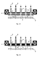
- Optisches System (10; 20) für ein Multistrahlsystem geladener Teilchen, umfassend
eine elektrostatische Linsenkomponente für eine Vielzahl von geladene Teilchenstrahlen (12) umfassend zumindest zwei elektrostatische Unterlinsen, wobei jede der Unterlinsen zumindest eine obere und eine untere Elektrode umfasst;
eine magnetische Linsenkomponente für eine Vielzahl von geladenen Teilchenstrahlen umfassend zumindest zwei magnetische Unterlinsen, wobei die Unterlinsen eine gemeinsame Erregerspule (15) teilen;
wobei die elektrostatische und die magnetische Linsenkomponente eine Multilinse für eine Vielzahl geladener Teilchenstrahlen bilden, umfassend zumindest zwei Unterlinsen;
wobei jede Unterlinse eine Öffnung (14) für einen geladenen Teilchenstrahl umfasst; und
wobei jede Unterlinse eingerichtet ist, einen geladenen Teilchenstrahl zu fokussieren. - Das optische System nach einem der vorangehenden Ansprüche, wobei eine der oberen und der unteren Elektrode von den zumindest zwei elektrostatischen Unterlinsen eine gemeinsame Elektrode (18) ist, wobei die gemeinsamen Elektroden der zumindest zwei elektrostatischen Unterlinsen auf einem gemeinsamen Potential liegen.
- Das optische System nach einem der vorangehenden Ansprüche, wobei die obere und untere Elektrode von jeder der zumindest zwei elektrostatischen Unterlinsen als die elektrostatische Linse konfiguriert ist, um weiterhin einen Elektronenstrahl zu fokussieren.
- Das optische System nach einem der vorangehenden Ansprüche, wobei die oberen Elektroden der zumindest zwei elektrostatischen Unterlinsen auf einem gemeinsamen Potential liegen, und die unteren Elektroden der zumindest zwei elektrostatischen Unterlinsen auf einem gemeinsamen Potential liegen.
- Das optische System nach einem der vorangehenden Ansprüche, wobei die elektrostatische Linsenkomponente für eine Vielzahl von geladenen Teilchenstrahlen eine Immersionslinsenkomponente für eine Vielzahl von geladenen Teilchenstrahlen ist.
- Das optische System nach einem der vorangehenden Ansprüche, wobei die elektrostatische Linsenkomponente für eine Vielzahl von geladenen Teilchenstrahlen eine Verzögerungslinsenkomponente für eine Vielzahl von geladenen Teilchenstrahlen ist.
- Das optische System (10; 20) nach einem der vorangehenden Ansprüche, wobei die magnetischen Unterlinsen Linsen mit radialem Spalt sind.
- Das optische System nach einem der Ansprüche 1 bis 6, wobei die magnetischen Unterlinsen Linsen mit axialem Spalt sind.
- Das optische System nach einem der Ansprüche 1 bis 6, wobei die magnetischen Unterlinsen Linsen mit radial-axialem Spalt sind.
- Das optische System nach einem der vorangehenden Ansprüche, wobei sich ein Linsenfeldbereich der elektrostatischen Unterlinse unter einem Linsenfeldbereich der entsprechenden magnetischen Unterlinse befindet.
- Das optische System nach einem der Ansprüche 1 bis 9, wobei sich ein Linsenfeldbereich der elektrostatischen Unterlinse über einem Linsenfeldbereich der entsprechenden magnetischen Unterlinse befindet.
- Das optische System nach einem der Ansprüche 1 bis 9, wobei sich ein Linsenfeldbereich der elektrostatischen Unterlinse und ein entsprechender Linsenfeldbereich der magnetischen Unterlinse überlappen.
- Das optische System nach einem der vorangehenden Ansprüche, wobei das Immersionsverhältnis des optischen Systems ungleich 1 ist.
- Das optische System (10; 20) nach einem der vorangehenden Ansprüche, umfassend Mittel (102; 112) zur individuellen Feineinstellung der fokussierenden Eigenschaften der Vielzahl der geladenen Teilchenstrahlen.
- Das optische System nach einem der vorangehenden Ansprüche, umfassend eine Extraktionselektrodenkomponente (122) mit einer Extraktionselektrode für jeden der zumindest zwei geladenen Teilchenstrahlen.
- Das optische System nach einem der vorangehenden Ansprüche, umfassend eine Scanablenkeinheit (144; 146; 152).
- Das optische System nach einem der vorangehenden Ansprüche, umfassend eine individuelle Scanablenkeinheit für jeden der zumindest zwei geladenen Teilchenstrahlen.
- Das optische System nach einem der Ansprüche 16 bis 17, wobei die Scanablenkeinheit eine Scanablenkeinheit (152) in der Linse ist.
- Das optische System nach einem der vorangehenden Ansprüche, umfassend eine Detektionseinheit (162; 174) zum Detektieren von Sekundärteilchen.
- Das optische System nach Anspruch 19, wobei die Detektionseinheit ein Spektrometer umfasst.
- Verfahren zum Fokussieren von zumindest zwei geladenen Teilchenstrahlen auf eine Probe, umfassend die Schritte:Bereitstellen eine optischen Systems mit
einer elektrostatischen Linsenkomponente für eine Vielzahl von geladenen Teilchenstrahlen, umfassend zumindest zwei elektrostatische Unterlinsen, wobei jede Unterlinse zumindest eine obere und eine untere Elektrode umfasst, und
einer magnetischen Linsenkomponente für eine Vielzahl von geladenen Teilchenstrahlen, umfassend zumindest zwei magnetische Unterlinsen, und
zumindest zwei separaten Öffnungen für jeden der zumindest zwei geladenen Teilchenstrahlen, die durch das optische System laufen,Kontrollieren eines Stroms für eine Erregerspule der magnetischen Linsenkomponente, dadurch Fokussieren der zumindest zwei Elektronenstrahlen;Kontrollieren von zumindest zwei Potentialen der elektrostatischen Linsenkomponente, dadurch Fokussieren der zumindest zwei Elektronenstrahlen. - Verfahren nach Anspruch 21, umfassend: getrennt Kontrollieren der obere Elektroden oder der unteren Elektroden für jede der zumindest zwei elektrostatischen Unterlinsen.
- Verfahren nach einem der Ansprüche 21 bis 22, weiterhin umfassend: Kontrollieren eines Korrekturmittels für Fokussiereigenschaften.
- Verfahren nach einem der Ansprüche 21 bis 23, weiterhin umfassend: Scannen der zumindest zwei geladenen Teilchenstrahlen über einen Bereich der Probe.
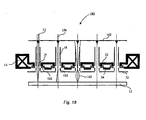
- Vorrichtung für einen Mehrfachstrahl geladener Teilchen, umfassend:eine Quelle für einen geladenen Teilchenstrahl (102);einen Detektor zum Detektieren von Sekundärteilchen (162);Strahl-formende Mittel (A);ein Gehäuse (191) für die Säule des geladenen Teilchenstrahls, wobei das Gehäuse evakuiert werden kann;zumindest ein optisches System (20; 180) nach einem der Ansprüche 1 bis 18, und zumindest eine Kontrolleinheit (7, 8, 9) für das zumindest eine optische System.
- Die Vorrichtung (190) für einen Mehrfachstrahl geladener Teilchen nach Anspruch 25, weiterhin umfassend eine Ablenkeinheit (172a, 172b) zum Leiten des geladenen Teilchenstrahls weg von der optischen Achse (11) und Umleiten des geladenen Teilchenstrahls.
- Die Vorrichtung für einen Mehrfachstrahl geladener Teilchen nach einem der Ansprüche 25 oder 26, wobei die Ablenkeinheit zumindest zwei magnetische Deflektoren (172a, 172b) umfasst.
- Die Vorrichtung für einen Mehrfachstrahl geladener Teilchen nach einem der Ansprüche 25 bis 27, wobei der Detektor ein Spektrometer umfasst.
Priority Applications (6)
| Application Number | Priority Date | Filing Date | Title |
|---|---|---|---|
| EP02028345A EP1432008B1 (de) | 2002-12-17 | 2002-12-17 | Mehrachsige Verbundlinse, Strahlvorrichtung und Verfahren zur Anwendung dieser kombinierten Linse |
| DE60236302T DE60236302D1 (de) | 2002-12-17 | 2002-12-17 | Mehrachsige Verbundlinse, Strahlvorrichtung und Verfahren zur Anwendung dieser kombinierten Linse |
| JP2004560384A JP4378290B2 (ja) | 2002-12-17 | 2003-12-12 | 多重軸複合レンズ、その複合レンズを用いたビーム系、およびその複合レンズの使用方法 |
| AU2003293862A AU2003293862A1 (en) | 2002-12-17 | 2003-12-12 | Multi-axis compound lens, beam system making use of the compound lens, and method using the compound lens |
| PCT/EP2003/014140 WO2004055856A2 (en) | 2002-12-17 | 2003-12-12 | Multi-axis compound lens, beam system making use of the compound lens, and method using the compound lens |
| US10/539,179 US7253417B2 (en) | 2002-12-17 | 2003-12-12 | Multi-axis compound lens, beam system making use of the compound lens, and method using the compound lens |
Applications Claiming Priority (1)
| Application Number | Priority Date | Filing Date | Title |
|---|---|---|---|
| EP02028345A EP1432008B1 (de) | 2002-12-17 | 2002-12-17 | Mehrachsige Verbundlinse, Strahlvorrichtung und Verfahren zur Anwendung dieser kombinierten Linse |
Publications (2)
| Publication Number | Publication Date |
|---|---|
| EP1432008A1 EP1432008A1 (de) | 2004-06-23 |
| EP1432008B1 true EP1432008B1 (de) | 2010-05-05 |
Family
ID=32338033
Family Applications (1)
| Application Number | Title | Priority Date | Filing Date |
|---|---|---|---|
| EP02028345A Expired - Lifetime EP1432008B1 (de) | 2002-12-17 | 2002-12-17 | Mehrachsige Verbundlinse, Strahlvorrichtung und Verfahren zur Anwendung dieser kombinierten Linse |
Country Status (6)
| Country | Link |
|---|---|
| US (1) | US7253417B2 (de) |
| EP (1) | EP1432008B1 (de) |
| JP (1) | JP4378290B2 (de) |
| AU (1) | AU2003293862A1 (de) |
| DE (1) | DE60236302D1 (de) |
| WO (1) | WO2004055856A2 (de) |
Families Citing this family (54)
| Publication number | Priority date | Publication date | Assignee | Title |
|---|---|---|---|---|
| DE60235636D1 (de) * | 2002-12-17 | 2010-04-22 | Integrated Circuit Testing | it dieser Linse, und Herstellungsverfahren für diese Linse |
| JP4824542B2 (ja) * | 2003-05-08 | 2011-11-30 | ザ サイエンス アンド テクノロジー ファシリティーズ カウンシル | 電子顕微鏡 |
| EP1657736B1 (de) * | 2004-11-15 | 2016-12-14 | ICT Integrated Circuit Testing Gesellschaft für Halbleiterprüftechnik mbH | Elektronenstrahlvorrichtung für hohe Stromdichten |
| US20090212213A1 (en) * | 2005-03-03 | 2009-08-27 | Ebara Corporation | Projection electron beam apparatus and defect inspection system using the apparatus |
| KR20070116260A (ko) * | 2005-03-22 | 2007-12-07 | 가부시키가이샤 에바라 세이사꾸쇼 | 전자선장치 |
| JP2007019192A (ja) * | 2005-07-06 | 2007-01-25 | Canon Inc | 荷電ビームレンズ、及び荷電ビーム露光装置 |
| WO2007013398A1 (ja) * | 2005-07-26 | 2007-02-01 | Ebara Corporation | 電子線装置 |
| EP1760762B1 (de) * | 2005-09-06 | 2012-02-01 | ICT Integrated Circuit Testing Gesellschaft für Halbleiterprüftechnik mbH | Vorrichtung und Verfahren zur Auswahl einer Emissionsfläche einer Emissionsstruktur |
| JP4878501B2 (ja) * | 2006-05-25 | 2012-02-15 | 株式会社日立ハイテクノロジーズ | 荷電粒子線応用装置 |
| JP2008066359A (ja) * | 2006-09-05 | 2008-03-21 | Canon Inc | 荷電ビームレンズアレイ、露光装置及びデバイス製造方法 |
| US7667208B2 (en) * | 2006-10-17 | 2010-02-23 | Varian Semiconductor Equipment Associates, Inc. | Technique for confining secondary electrons in plasma-based ion implantation |
| JP2010509709A (ja) | 2006-10-24 | 2010-03-25 | ビー・ナノ・リミテッド | インターフェース、非真空環境内で物体を観察する方法、および走査型電子顕微鏡 |
| JP5227512B2 (ja) * | 2006-12-27 | 2013-07-03 | 株式会社日立ハイテクノロジーズ | 電子線応用装置 |
| US8642959B2 (en) | 2007-10-29 | 2014-02-04 | Micron Technology, Inc. | Method and system of performing three-dimensional imaging using an electron microscope |
| WO2009113169A1 (ja) * | 2008-03-13 | 2009-09-17 | 株式会社アドバンテスト | マルチコラム電子ビーム露光装置 |
| US8981294B2 (en) | 2008-07-03 | 2015-03-17 | B-Nano Ltd. | Scanning electron microscope, an interface and a method for observing an object within a non-vacuum environment |
| US9405203B2 (en) | 2008-09-23 | 2016-08-02 | Applied Materials, Inc. | Pixel blending for multiple charged-particle beam lithography |
| US8253923B1 (en) | 2008-09-23 | 2012-08-28 | Pinebrook Imaging Technology, Ltd. | Optical imaging writer system |
| US8670106B2 (en) | 2008-09-23 | 2014-03-11 | Pinebrook Imaging, Inc. | Optical imaging writer system |
| EP2329252A4 (de) * | 2008-09-28 | 2012-04-11 | Nano Ltd B | Vakuumvorrichtung und elektronenmikroskop |
| DE102008062450B4 (de) * | 2008-12-13 | 2012-05-03 | Vistec Electron Beam Gmbh | Anordnung zur Beleuchtung eines Substrats mit mehreren individuell geformten Partikelstrahlen zur hochauflösenden Lithographie von Strukturmustern |
| JP5634052B2 (ja) * | 2009-01-09 | 2014-12-03 | キヤノン株式会社 | 荷電粒子線描画装置およびデバイス製造方法 |
| KR20120098627A (ko) | 2009-09-18 | 2012-09-05 | 마퍼 리쏘그라피 아이피 비.브이. | 다중 빔을 갖는 대전 입자 광학 시스템 |
| US8003953B2 (en) | 2009-12-11 | 2011-08-23 | Hermes Microvision, Inc. | Multi-axis magnetic lens |
| US8399852B2 (en) * | 2010-11-24 | 2013-03-19 | Alexander Klein | Systems and methods for control of multiple charged particle beams |
| US8445862B2 (en) * | 2010-12-14 | 2013-05-21 | Hermes Microvision, Inc. | Apparatus of plural charged particle beams with multi-axis magnetic lens |
| US8294095B2 (en) | 2010-12-14 | 2012-10-23 | Hermes Microvision, Inc. | Apparatus of plural charged particle beams with multi-axis magnetic lens |
| TWI593961B (zh) | 2010-12-15 | 2017-08-01 | 日立全球先端科技股份有限公司 | Charged particle line application device, and irradiation method |
| JP5749028B2 (ja) * | 2011-02-11 | 2015-07-15 | 株式会社ホロン | 走査型電子顕微鏡 |
| EP2913837B1 (de) * | 2011-02-18 | 2020-07-29 | Applied Materials Israel Ltd. | Fokussierung eines abbildungssystems mit geladenen teilchen |
| NL2006868C2 (en) * | 2011-05-30 | 2012-12-03 | Mapper Lithography Ip Bv | Charged particle multi-beamlet apparatus. |
| US8455838B2 (en) * | 2011-06-29 | 2013-06-04 | Kla-Tencor Corporation | Multiple-column electron beam apparatus and methods |
| JP5970213B2 (ja) * | 2012-03-19 | 2016-08-17 | 株式会社ニューフレアテクノロジー | マルチ荷電粒子ビーム描画装置及びマルチ荷電粒子ビーム描画方法 |
| NL2009053C2 (en) | 2012-06-22 | 2013-12-24 | Univ Delft Tech | Apparatus and method for inspecting a surface of a sample. |
| JP2014116518A (ja) * | 2012-12-11 | 2014-06-26 | Canon Inc | 描画装置及び物品の製造方法 |
| JP6087154B2 (ja) * | 2013-01-18 | 2017-03-01 | 株式会社ニューフレアテクノロジー | 荷電粒子ビーム描画装置、試料面へのビーム入射角調整方法、および荷電粒子ビーム描画方法 |
| JP2016513349A (ja) | 2013-02-20 | 2016-05-12 | ビー−ナノ リミテッド | 走査型電子顕微鏡 |
| KR102166879B1 (ko) * | 2014-03-10 | 2020-10-16 | 어플라이드 머티어리얼스, 인코포레이티드 | 다중 하전-입자 빔 리소그래피를 위한 픽셀 블렌딩 |
| US9431209B2 (en) | 2014-08-26 | 2016-08-30 | Hermes-Microvision, Inc. | Apparatus of plural charged particle beams with multi-axis magnetic lenses |
| EP3010031B1 (de) * | 2014-10-16 | 2017-03-22 | Fei Company | Geladenes Teilchenmikroskop mit spezieller Aperturplatte |
| US9922799B2 (en) * | 2015-07-21 | 2018-03-20 | Hermes Microvision, Inc. | Apparatus of plural charged-particle beams |
| JP6684586B2 (ja) * | 2015-12-22 | 2020-04-22 | 株式会社ニューフレアテクノロジー | マルチ荷電粒子ビーム装置 |
| US9984848B2 (en) * | 2016-03-10 | 2018-05-29 | ICT Integrated Circuit Testing Gesellschaft für Halbleiterprüftechnik mbH | Multi-beam lens device, charged particle beam device, and method of operating a multi-beam lens device |
| US10157723B2 (en) | 2016-08-03 | 2018-12-18 | Nuflare Technology, Inc. | Multi charged particle beam writing apparatus and method of adjusting the same |
| US10453645B2 (en) * | 2016-12-01 | 2019-10-22 | Applied Materials Israel Ltd. | Method for inspecting a specimen and charged particle multi-beam device |
| US11101106B2 (en) | 2017-04-11 | 2021-08-24 | Advantest Corporation | Exposure device |
| US10354832B2 (en) * | 2017-06-07 | 2019-07-16 | Kla-Tencor Corporation | Multi-column scanning electron microscopy system |
| US10395887B1 (en) * | 2018-02-20 | 2019-08-27 | Technische Universiteit Delft | Apparatus and method for inspecting a surface of a sample, using a multi-beam charged particle column |
| US10504687B2 (en) | 2018-02-20 | 2019-12-10 | Technische Universiteit Delft | Signal separator for a multi-beam charged particle inspection apparatus |
| NL2020465B1 (en) * | 2018-02-20 | 2019-08-29 | Univ Delft Tech | Apparatus and method for inspecting a surface of a sample, using a multi-beam charged particle column |
| EP3834222A1 (de) * | 2018-08-09 | 2021-06-16 | ASML Netherlands B.V. | Vorrichtung für mehrere ladungsteilchenstrahlen |
| EP3618095A1 (de) * | 2018-08-28 | 2020-03-04 | ASML Netherlands B.V. | Verfahren und systeme zur inspektion mit mehreren elektronenstrahlen |
| DE102018007652B4 (de) * | 2018-09-27 | 2021-03-25 | Carl Zeiss Multisem Gmbh | Teilchenstrahl-System sowie Verfahren zur Stromregulierung von Einzel-Teilchenstrahlen |
| JP2023509397A (ja) * | 2020-01-06 | 2023-03-08 | エーエスエムエル ネザーランズ ビー.ブイ. | 荷電粒子評価ツール、検査方法 |
Citations (1)
| Publication number | Priority date | Publication date | Assignee | Title |
|---|---|---|---|---|
| WO2001039243A1 (en) * | 1999-11-23 | 2001-05-31 | Ion Diagnostics, Inc. | Electron optics for multi-beam electron beam lithography tool |
Family Cites Families (5)
| Publication number | Priority date | Publication date | Assignee | Title |
|---|---|---|---|---|
| DE19605855A1 (de) * | 1996-02-16 | 1997-08-21 | Act Advanced Circuit Testing | Detektorobjektiv für Korpuskularstrahlgeräte |
| WO2001075949A1 (fr) * | 2000-04-04 | 2001-10-11 | Advantest Corporation | Appareil d'exposition multifaisceau comprenant une lentille electronique multiaxe, et procede de fabrication d'un dispositif a semi-conducteur |
| JP4535602B2 (ja) * | 2000-11-13 | 2010-09-01 | 株式会社アドバンテスト | 電子ビーム露光装置及び電子レンズ |
| US6750455B2 (en) * | 2001-07-02 | 2004-06-15 | Applied Materials, Inc. | Method and apparatus for multiple charged particle beams |
| JP2003203836A (ja) * | 2001-12-28 | 2003-07-18 | Canon Inc | 露光装置及びその制御方法並びにデバイス製造方法 |
-
2002
- 2002-12-17 DE DE60236302T patent/DE60236302D1/de not_active Expired - Lifetime
- 2002-12-17 EP EP02028345A patent/EP1432008B1/de not_active Expired - Lifetime
-
2003
- 2003-12-12 US US10/539,179 patent/US7253417B2/en not_active Expired - Lifetime
- 2003-12-12 JP JP2004560384A patent/JP4378290B2/ja not_active Expired - Lifetime
- 2003-12-12 AU AU2003293862A patent/AU2003293862A1/en not_active Abandoned
- 2003-12-12 WO PCT/EP2003/014140 patent/WO2004055856A2/en active Application Filing
Patent Citations (1)
| Publication number | Priority date | Publication date | Assignee | Title |
|---|---|---|---|---|
| WO2001039243A1 (en) * | 1999-11-23 | 2001-05-31 | Ion Diagnostics, Inc. | Electron optics for multi-beam electron beam lithography tool |
Also Published As
| Publication number | Publication date |
|---|---|
| US20060169910A1 (en) | 2006-08-03 |
| EP1432008A1 (de) | 2004-06-23 |
| AU2003293862A1 (en) | 2004-07-09 |
| AU2003293862A8 (en) | 2004-07-09 |
| WO2004055856A2 (en) | 2004-07-01 |
| JP4378290B2 (ja) | 2009-12-02 |
| DE60236302D1 (de) | 2010-06-17 |
| JP2006510184A (ja) | 2006-03-23 |
| WO2004055856A3 (en) | 2004-08-12 |
| US7253417B2 (en) | 2007-08-07 |
Similar Documents
| Publication | Publication Date | Title |
|---|---|---|
| EP1432008B1 (de) | Mehrachsige Verbundlinse, Strahlvorrichtung und Verfahren zur Anwendung dieser kombinierten Linse | |
| KR102214294B1 (ko) | 1차 하전 입자 빔렛들의 어레이를 이용한 시료의 검사를 위한 하전 입자 빔 디바이스 | |
| CN109427524B (zh) | 带电粒子束装置、用于带电粒子束装置的孔布置和用于操作带电粒子束装置的方法 | |
| EP2879155B1 (de) | Mehrstrahlsystem mit Hochdurchsatz-EBI | |
| JP5710061B2 (ja) | 高スループットsemツール | |
| US9153413B2 (en) | Multi-beam scanning electron beam device and methods of using the same | |
| US9997326B2 (en) | Charged particle beam device | |
| WO2001084592A1 (en) | Multi beam charged particle device | |
| CN210136840U (zh) | 用于带电粒子束装置的带电粒子束转储器和多束带电粒子束装置 | |
| US20060033035A1 (en) | Electron microscope array for inspection and lithography | |
| JP2023063390A (ja) | 電磁複合レンズ及びそのようなレンズを備えた荷電粒子光学システム | |
| US20240006147A1 (en) | Flood column and charged particle apparatus |
Legal Events
| Date | Code | Title | Description |
|---|---|---|---|
| PUAI | Public reference made under article 153(3) epc to a published international application that has entered the european phase |
Free format text: ORIGINAL CODE: 0009012 |
|
| AK | Designated contracting states |
Kind code of ref document: A1 Designated state(s): AT BE BG CH CY CZ DE DK EE ES FI FR GB GR IE IT LI LU MC NL PT SE SI SK TR |
|
| AX | Request for extension of the european patent |
Extension state: AL LT LV MK RO |
|
| 17P | Request for examination filed |
Effective date: 20041118 |
|
| AKX | Designation fees paid |
Designated state(s): DE GB NL |
|
| 17Q | First examination report despatched |
Effective date: 20071004 |
|
| GRAP | Despatch of communication of intention to grant a patent |
Free format text: ORIGINAL CODE: EPIDOSNIGR1 |
|
| RAP1 | Party data changed (applicant data changed or rights of an application transferred) |
Owner name: ICT, INTEGRATED CIRCUIT TESTING GESELLSCHAFT FUER |
|
| GRAS | Grant fee paid |
Free format text: ORIGINAL CODE: EPIDOSNIGR3 |
|
| GRAA | (expected) grant |
Free format text: ORIGINAL CODE: 0009210 |
|
| AK | Designated contracting states |
Kind code of ref document: B1 Designated state(s): DE GB NL |
|
| REG | Reference to a national code |
Ref country code: GB Ref legal event code: FG4D |
|
| REF | Corresponds to: |
Ref document number: 60236302 Country of ref document: DE Date of ref document: 20100617 Kind code of ref document: P |
|
| REG | Reference to a national code |
Ref country code: NL Ref legal event code: T3 |
|
| PLBE | No opposition filed within time limit |
Free format text: ORIGINAL CODE: 0009261 |
|
| STAA | Information on the status of an ep patent application or granted ep patent |
Free format text: STATUS: NO OPPOSITION FILED WITHIN TIME LIMIT |
|
| PGFP | Annual fee paid to national office [announced via postgrant information from national office to epo] |
Ref country code: GB Payment date: 20101123 Year of fee payment: 9 |
|
| 26N | No opposition filed |
Effective date: 20110208 |
|
| REG | Reference to a national code |
Ref country code: DE Ref legal event code: R097 Ref document number: 60236302 Country of ref document: DE Effective date: 20110207 |
|
| GBPC | Gb: european patent ceased through non-payment of renewal fee |
Effective date: 20111217 |
|
| PG25 | Lapsed in a contracting state [announced via postgrant information from national office to epo] |
Ref country code: GB Free format text: LAPSE BECAUSE OF NON-PAYMENT OF DUE FEES Effective date: 20111217 |
|
| PGFP | Annual fee paid to national office [announced via postgrant information from national office to epo] |
Ref country code: DE Payment date: 20191119 Year of fee payment: 18 |
|
| REG | Reference to a national code |
Ref country code: DE Ref legal event code: R119 Ref document number: 60236302 Country of ref document: DE |
|
| PG25 | Lapsed in a contracting state [announced via postgrant information from national office to epo] |
Ref country code: DE Free format text: LAPSE BECAUSE OF NON-PAYMENT OF DUE FEES Effective date: 20210701 |
|
| PGFP | Annual fee paid to national office [announced via postgrant information from national office to epo] |
Ref country code: NL Payment date: 20211118 Year of fee payment: 20 |
|
| REG | Reference to a national code |
Ref country code: NL Ref legal event code: MK Effective date: 20221216 |