WO2009113169A1 - マルチコラム電子ビーム露光装置 - Google Patents
マルチコラム電子ビーム露光装置 Download PDFInfo
- Publication number
- WO2009113169A1 WO2009113169A1 PCT/JP2008/054594 JP2008054594W WO2009113169A1 WO 2009113169 A1 WO2009113169 A1 WO 2009113169A1 JP 2008054594 W JP2008054594 W JP 2008054594W WO 2009113169 A1 WO2009113169 A1 WO 2009113169A1
- Authority
- WO
- WIPO (PCT)
- Prior art keywords
- electron beam
- column
- lens
- coil
- exposure apparatus
- Prior art date
Links
- 238000010894 electron beam technology Methods 0.000 title claims abstract description 116
- 238000000206 photolithography Methods 0.000 title abstract 3
- 230000004075 alteration Effects 0.000 claims abstract description 26
- 201000009310 astigmatism Diseases 0.000 claims description 20
- 238000010586 diagram Methods 0.000 description 23
- 230000003287 optical effect Effects 0.000 description 17
- 239000000758 substrate Substances 0.000 description 14
- 238000004088 simulation Methods 0.000 description 4
- 230000001678 irradiating effect Effects 0.000 description 2
- 230000001133 acceleration Effects 0.000 description 1
- 238000006243 chemical reaction Methods 0.000 description 1
- 238000000034 method Methods 0.000 description 1
- 238000007493 shaping process Methods 0.000 description 1
Images


Classifications
-
- H—ELECTRICITY
- H01—ELECTRIC ELEMENTS
- H01J—ELECTRIC DISCHARGE TUBES OR DISCHARGE LAMPS
- H01J37/00—Discharge tubes with provision for introducing objects or material to be exposed to the discharge, e.g. for the purpose of examination or processing thereof
- H01J37/02—Details
- H01J37/04—Arrangements of electrodes and associated parts for generating or controlling the discharge, e.g. electron-optical arrangement or ion-optical arrangement
- H01J37/10—Lenses
- H01J37/14—Lenses magnetic
- H01J37/141—Electromagnetic lenses
-
- B—PERFORMING OPERATIONS; TRANSPORTING
- B82—NANOTECHNOLOGY
- B82Y—SPECIFIC USES OR APPLICATIONS OF NANOSTRUCTURES; MEASUREMENT OR ANALYSIS OF NANOSTRUCTURES; MANUFACTURE OR TREATMENT OF NANOSTRUCTURES
- B82Y10/00—Nanotechnology for information processing, storage or transmission, e.g. quantum computing or single electron logic
-
- B—PERFORMING OPERATIONS; TRANSPORTING
- B82—NANOTECHNOLOGY
- B82Y—SPECIFIC USES OR APPLICATIONS OF NANOSTRUCTURES; MEASUREMENT OR ANALYSIS OF NANOSTRUCTURES; MANUFACTURE OR TREATMENT OF NANOSTRUCTURES
- B82Y40/00—Manufacture or treatment of nanostructures
-
- H—ELECTRICITY
- H01—ELECTRIC ELEMENTS
- H01J—ELECTRIC DISCHARGE TUBES OR DISCHARGE LAMPS
- H01J37/00—Discharge tubes with provision for introducing objects or material to be exposed to the discharge, e.g. for the purpose of examination or processing thereof
- H01J37/02—Details
- H01J37/04—Arrangements of electrodes and associated parts for generating or controlling the discharge, e.g. electron-optical arrangement or ion-optical arrangement
- H01J37/153—Electron-optical or ion-optical arrangements for the correction of image defects, e.g. stigmators
-
- H—ELECTRICITY
- H01—ELECTRIC ELEMENTS
- H01J—ELECTRIC DISCHARGE TUBES OR DISCHARGE LAMPS
- H01J37/00—Discharge tubes with provision for introducing objects or material to be exposed to the discharge, e.g. for the purpose of examination or processing thereof
- H01J37/30—Electron-beam or ion-beam tubes for localised treatment of objects
- H01J37/317—Electron-beam or ion-beam tubes for localised treatment of objects for changing properties of the objects or for applying thin layers thereon, e.g. for ion implantation
- H01J37/3174—Particle-beam lithography, e.g. electron beam lithography
- H01J37/3177—Multi-beam, e.g. fly's eye, comb probe
Definitions
- the present invention relates to a multi-column electron beam exposure apparatus, and more particularly to a multi-column electron beam exposure apparatus that enables an electromagnetic lens of each column cell to be axisymmetric.
- a variable rectangular opening or a plurality of stencil mask patterns are prepared in a stencil mask, and these are selected by beam deflection and transferred and exposed on a wafer.
- Patent Document 1 discloses an electron beam exposure apparatus that performs partial batch exposure.
- a beam is irradiated to a single pattern region selected by beam deflection from a plurality of, for example, 100 stencil patterns arranged on a mask, for example, a 20 ⁇ 20 ⁇ m region, and the beam cross section is formed into a stencil pattern shape.
- the beam that has been shaped and then passed through the mask is deflected back by a subsequent deflector, reduced to a constant reduction rate determined by the electron optical system, for example, 1/10, and transferred to the sample surface.
- the stencil pattern on the mask is appropriately prepared according to the device pattern to be exposed, the number of exposure shots required is greatly reduced and the throughput is improved as compared with the case of only the variable rectangular aperture.
- a multi-column electron beam exposure apparatus that collects a plurality of such columns each having a smaller size (hereinafter referred to as a column cell) and performs exposure processing in parallel on a wafer.
- Each column cell is equivalent to the column of a single column electron beam exposure apparatus, but the entire multi-column processes in parallel, so that the exposure throughput can be increased by the number of columns.
- the column cells are required to be equivalent.
- a multi-column electron beam exposure system for example, when an electromagnetic lens is used to converge the beam by an electromagnetic lens and each current is applied, the same function is exhibited due to the configuration of the electromagnetic lens and the difference in applied current between each column. There is a risk that it cannot be done. Therefore, if it is common to each column, it is desirable to make it one. By making common, the distance between the columns can be reduced, and the entire apparatus can be made compact.
- the present invention has been made in view of the problems of the prior art, and an object thereof is to provide a multi-column electron beam exposure apparatus capable of making the electromagnetic lens of each column cell uniform and axially symmetric.
- the above-described problem is a multi-column electron beam exposure apparatus including a plurality of column cells, and each column cell includes two magnetic pole plates provided with openings through which electron beams used in each column cell pass. At least 6 poles inside the lens formed between the pair of openings of the electromagnetic lens or outside the lens above the opening. This is solved by a multi-column electron beam exposure apparatus in which a deflection aberration corrector is arranged.
- the deflection aberration corrector may be configured by an electromagnet that is reversely wound every 60 degrees and has substantially the same number of turns.
- the two pairs of deflection aberration correctors may be arranged at the same height inside the lens and at the same or different height outside the lens. You may be made to do.
- a quadrupole deflector for deflecting the electron beam in the XY directions is disposed on a side surface of the opening, and the lens is formed between the pair of openings. Further, a focus correction coil and an astigmatism correction coil may be arranged, and an alignment coil for deflecting the electron beam into the lens may be arranged outside the lens above the opening.
- a small lens opening is formed by a circular hole through which the electron beam of each column cell passes through an electromagnetic lens common to a plurality of column cells.
- the small lens aperture is provided with a correction coil for converging the electron beam on the optical axis.
- the correction coil includes a focus correction coil, an XY-direction deflection coil, an astigmatism correction coil, an alignment coil for irradiating the circular hole with an electron beam, and a beam shape aberration correction coil for correcting the beam shape to a circle. It is.
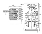
- FIG. 1 is a block diagram of a multi-column electron beam exposure apparatus according to the present invention.
- FIG. 2 is a block diagram of one column cell in the exposure apparatus according to FIG.
- FIG. 3 is a schematic diagram of a column cell control unit of the exposure apparatus according to FIG.
- FIG. 4 is a view schematically showing the electromagnetic lens portion of the multi-column electron beam exposure apparatus.
- FIGS. 5A and 5B are diagrams showing problems with the electromagnetic lens of the multi-column electron beam exposure apparatus.
- FIGS. 6A and 6B are diagrams schematically showing a one-stage electromagnetic lens.
- FIG. 7 is a diagram (part 1) schematically illustrating the correction coil.
- FIG. 8 is a diagram (part 2) schematically illustrating the correction coil.
- FIG. 7 is a diagram (part 1) schematically illustrating the correction coil.
- FIG. 9 is a diagram showing an example of an astigmatism correction coil.
- FIGS. 10A and 10B are diagrams for explaining how the electron beam is converged by the electromagnetic lens.
- FIG. 11A is a diagram illustrating an example of a beam shape
- FIG. 11B is a diagram illustrating a hexapole coil that corrects the beam shape of FIG. 11A.
- FIG. 12 is a diagram for explaining the symmetry of the magnetic lens.
- FIG. 1 is a schematic block diagram of a multi-column electron beam exposure apparatus according to this embodiment.
- the multi-column electron beam exposure apparatus is roughly divided into an electron beam column 10 and a controller 20 that controls the electron beam column 10.
- the electron beam column 10 is composed of a plurality of equivalent column cells 11, for example, 16 to form an entire column. All the column cells 11 are composed of the same unit described later. Under the column cell 11, for example, a wafer stage 13 on which a 300 mm wafer 12 is mounted is disposed.
- the control unit 20 includes an electron gun high-voltage power supply 21, a lens power supply 22, a digital control unit 23, a stage drive controller 24, and a stage position sensor 25.
- the electron gun high-voltage power supply 21 supplies power for driving the electron gun of each column cell 11 in the electron beam column 10.
- the lens power supply 22 supplies power for driving the electromagnetic lens of each column cell 11 in the electron beam column 10.
- the digital control unit 23 is an electric circuit that controls the deflection output of each deflector in the column cell 11 and outputs a high-speed deflection output or the like. The number of digital control units 23 corresponding to the number of column cells 11 is prepared.
- the stage drive controller 24 moves the wafer stage 13 based on the position information from the stage position sensor 25 so that the desired position of the wafer 12 is irradiated with the electron beam.
- the above-described units 21 to 25 are controlled in an integrated manner by an integrated control system 26 such as a workstation.
- all the column cells 11 are composed of the same column unit.
- FIG. 2 is a schematic configuration diagram of each column cell 11 used in the multi-column electron beam exposure apparatus.
- Each column cell 11 is roughly divided into an exposure unit 100 and a column cell control unit 31 that controls the exposure unit 100.
- the exposure unit 100 includes an electron beam generation unit 130, a mask deflection unit 140, and a substrate deflection unit 150.
- the electron beam EB generated from the electron gun 101 is converged by the first electromagnetic lens 102, then passes through the rectangular aperture 103 a of the beam shaping mask 103, and the electron beam EB has a rectangular cross section. To be molded.
- the electron beam EB is imaged on the exposure mask 110 by the second electromagnetic lens 105 of the mask deflection unit 140. Then, the electron beam EB is deflected to a specific pattern P formed on the exposure mask 110 by the first and second electrostatic deflectors 104 and 106, and the cross-sectional shape thereof is formed into the pattern P shape.
- the exposure mask 110 is fixed to a mask stage 123 in the electron beam column 10, but the mask stage 123 is movable in a horizontal plane, and the deflection range of the first and second electrostatic deflectors 104 and 106.
- the pattern P is moved into the beam deflection area by moving the mask stage 123.
- the third and fourth electromagnetic lenses 108 and 111 arranged above and below the exposure mask 110 play a role of forming an image of the electron beam EB on the substrate by adjusting their current amounts.
- the electron beam EB that has passed through the exposure mask 110 is returned to the optical axis C by the deflection action of the third and fourth electrostatic deflectors 112 and 113 and then reduced in size by the fifth electromagnetic lens 114.
- the mask deflection unit 140 is provided with first and second correction coils 107 and 109, which correct beam deflection aberrations generated by the first to fourth electrostatic deflectors 104, 106, 112, and 113. Is done.
- the electron beam EB passes through the aperture 115 a of the shielding plate 115 constituting the substrate deflecting unit 150 and is projected onto the substrate by the first and second projection electromagnetic lenses 116 and 121.
- the pattern image of the exposure mask 110 is transferred to the substrate at a predetermined reduction ratio, for example, a reduction ratio of 1/10.
- the substrate deflecting unit 150 is provided with a fifth electrostatic deflector 119 and an electromagnetic deflector 120, and the electron beam EB is deflected by these deflectors 119 and 120, and the exposure mask is placed at a predetermined position on the substrate. An image of the pattern is projected.
- the substrate deflection unit 150 is provided with third and fourth correction coils 117 and 118 for correcting the deflection aberration of the electron beam EB on the substrate.
- the column cell control unit 31 includes an electron gun control unit 202, an electron optical system control unit 203, a mask deflection control unit 204, a mask stage control unit 205, a blanking control unit 206, and a substrate deflection control unit 207.
- the electron gun control unit 202 controls the electron gun 101 to control the acceleration voltage of the electron beam EB, beam emission conditions, and the like.
- the electron optical system control unit 203 controls the amount of current to the electromagnetic lenses 102, 105, 108, 111, 114, 116 and 121, and the magnification and focus of the electron optical system in which these electromagnetic lenses are configured. Adjust the position.
- the blanking control unit 206 controls the voltage applied to the blanking electrode 127 to deflect the electron beam EB generated before the start of exposure onto the shielding plate 115, and before the exposure, the electron beam EB is applied onto the substrate. Is prevented from being irradiated.
- the substrate deflection control unit 207 controls the applied voltage to the fifth electrostatic deflector 119 and the amount of current to the electromagnetic deflector 120 so that the electron beam EB is deflected to a predetermined position on the substrate. To do.
- the above-described units 202 to 207 are controlled in an integrated manner by an integrated control system 26 such as a workstation.
- FIG. 3 is a schematic diagram of the column cell control unit 31 in the multi-column electron beam exposure apparatus.
- Each column cell 11 has a column cell control unit 31.
- Each column cell control unit 31 is connected by a bus 34 to an integrated control system 26 that controls the entire multi-column electron beam exposure apparatus.
- the integrated storage unit 33 stores data necessary for all column cells such as exposure data.
- the integrated storage unit 33 is also connected to the integrated control system 26 via the bus 34.
- exposure data of a pattern to be exposed on the wafer 12 placed on the wafer stage 13 is transferred from the integrated storage unit 33 to the column cell storage unit 35 of each column cell control unit 31. Forward to.
- the transferred exposure data is corrected by the correction unit 36 of each column cell control unit 31, converted into data actually required for the exposure processing by the exposure data conversion unit 37, and assigned to each column cell 11.
- the same pattern is exposed in the upper exposure area.
- magnification and rotation of an image projected onto a substrate are adjusted using an electron optical system, and the focal position of the image is adjusted.
- the magnetic field is changed by changing the current flowing through the coil.
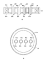
- FIG. 4 is a diagram schematically showing an electromagnetic lens portion of the multi-column electron beam exposure apparatus.
- FIG. 4 shows an apparatus having four column cells. One sample 13 is exposed by electron beams EB1 to EB4 irradiated by electron guns 43a to 43d.
- this apparatus includes four stages of electromagnetic lenses 41a to 41d.
- the electromagnetic lens 41a includes a coil 42a that supplies a magnetic field in common to all the column cells, and a magnetic pole plate is installed so as to sandwich the coil 42a.
- the magnetic pole plate is provided with openings 44a to 44d for allowing an electron beam to pass. Yes. In each opening, correction coils 45a to 45d for correcting the magnetic field generated by the coil 42a are provided.
- FIG. 5 is a diagram showing problems with the electromagnetic lens of the multi-column electron beam exposure apparatus.
- FIG. 5A is a diagram showing the focus of the electron beam when the electromagnetic lens of each column cell is configured by only the coil 52 common to the entire column cell of the apparatus. As shown in FIG. 5A, when the electron beam is irradiated under the same conditions, the focal length of the electromagnetic lens in the column cells on both sides is shorter than that in the central column cell so that the focal length of the electromagnetic lens is reduced. Simulations reveal that the distances are different.
- This factor may be that the coils are wound in common and that the magnetic poles of the multi-column cell magnetic field are not uniform between the parallel plate magnetic poles.
- the coils are independent in each column, adjustment such as supplying the same current is difficult, and there is a possibility that an error will increase between the columns. Therefore, in this embodiment, correction is performed on the lenses in each column cell while using the entire common coil.
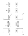
- FIG. 6 is a diagram schematically showing a one-stage electromagnetic lens provided with a correction coil.
- FIG. 6A is a sectional view
- FIG. 6B is a plan view.
- the electromagnetic lens 61 of the multi-column electron beam exposure apparatus includes a coil 62 that is commonly used for the entire column cell, and two upper and lower magnetic pole plates (pole pieces) 61a sandwiching the coil 62. 61b.
- the pole plate is provided with openings (circular holes) 63a to 63d through which the electron beams EB1 to EB4 of the column cells pass, and correction coils 64a to 64d are provided in the vicinity of the openings. This opening is called a small lens opening for convenience.
- each column cell In order to make the electromagnetic lens by the small lens aperture of each column cell axially symmetric, it is required to deflect the electron beam to the optical axis and correct the positional deviation in the height direction of the image. In addition, when the electron beam is deflected, an aberration associated with the deflection is generated, and it is required to correct the aberration. Furthermore, it is required to eliminate the factor of beam blur that has been found out as a result of simulation described later.
- FIG 7 and 8 are diagrams showing in detail the correction coil provided in the small lens opening to satisfy these requirements.
- the correction coil includes an alignment coil 71 for allowing the electron beam to pass through the circular hole, a Z-direction correction (focus correction) coil 74, an astigmatism correction coil 75, and an electron beam for deflecting the electron beam in the XY direction.
- the XY deflection coils 73a and 73b and a beam shape aberration correction coil 72 for correcting the cross-sectional shape of the electron beam to a circle are constituted by five types of coils.
- the focus correction coil 74 is a circular coil centered on the optical axis, and adjusts the focus position by correcting the magnetic field in the Z-axis direction (height direction) of the electron beam.
- the astigmatism correction coil 75 corrects astigmatism inherent to the electron lens and astigmatism due to deflection of the electron beam, and is composed of an 8-pole coil shifted by 45 degrees.
- An astigmatism is produced by adjusting the amount of current so that a magnetic field is generated by applying a current to the astigmatism correction coil to generate a magnetic field, exerting a force on the electron beam, and generating a magnetic field that makes the elliptical beam cross-section circular. Correct aberrations.
- FIG. 9 is a view showing an example of the astigmatism correction coil 75.
- FIG. 9A is a plan view of the astigmatism correction coil 75
- FIG. 9B is a plan view schematically showing the operating principle of the coil of FIG. 9A.
- the astigmatism correction coil 75 has two sets of quadrupole coils 81a and 81b.
- the two sets of quadrupole coils 81a and 81b are arranged so that the coils of each set are alternately wound in opposite directions, and the axis of the coils is radial with respect to the optical axis (Z axis). Has been.
- the two sets of quadrupole coils 81a and 81b are driven by the two sets of power sources Ia and Ib, respectively.
- One series of coils 81a1 to 81a4 is connected to the power source Ia, and the other series of coils 81b1 to 81b4 is connected to the power source Ib.
- FIG. 9B shows a set of coils 81a1 to 81a4 connected in series among the two sets of quadrupole coils 81a and 81b of FIG. 9A.
- the electron beam receives a force approaching the optical axis in the upper right and lower left regions, and in the lower right and upper left regions, the force is applied in a direction away from the optical axis. receive.
- the electron beam passing through the magnetic field of the astigmatism correction coil in FIG. 9B is compressed in the right oblique direction, expanded in the direction orthogonal thereto, and elongated astigmatism is produced in the right oblique direction. Canceled.
- Astigmatism in various directions is corrected by controlling the current supplied from the power supply to each coil.
- the alignment coil 71 is a coil provided to allow the electron beam to pass through the circular hole 63, and is composed of two upper and lower quadrupole coils above each small lens opening. A mode in which the two coils are interlocked to deflect the electron beam is combined so that the electron beam is incident on the lens center along the axis.
- a mode for deflecting the electron beam for example, there are a shift mode in which the direction of the incident electron beam is shifted in the lateral direction and a pivot mode in which the direction of the electron beam is changed around a certain fulcrum. The electron beam is moved to the aperture in the shift mode, and then the direction of the electron beam is swung with the aperture center as a fulcrum in the pivot mode, and control is performed so as to enter the lens center along the axis.
- the XY deflection coils 73a and 73b are configured by installing a quadrupole deflector on the side surface of the circular hole of each of the upper and lower magnetic pole plates.
- the quadrupole deflector is composed of a four-pole coil shifted by 90 degrees as shown in FIG. 9B, and a current is passed through the coil to generate a magnetic field to correct the position of the electron beam in the XY directions.
- the beam shape aberration correction coil 72 is a coil that corrects the shape of the beam immediately before convergence to a shape close to a circle, and is a position in the electromagnetic lens between the small lens openings between the circular holes or a position before entering the electromagnetic lens. Two hexapole coils are installed.
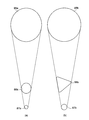
- FIG. 10 is a diagram for explaining how the electron beam is converged by the electromagnetic lens.
- FIG. 10A shows a case where the electromagnetic lens is normal
- FIG. 10B shows a case where the electromagnetic lens has aberration.
- FIG. 10 (b) is a result of simulating the trajectory of the electron beam irradiated with no correction coil installed, and it has been found that the beam near the focal point has a diameter of about 6 nm and the beam shape is blurred. In this simulation, it was found that when the shape of the beam immediately before the focal point was calculated, a substantially triangular shape 86b was obtained as shown in FIG.
- the cross-sectional shape of the electron beam is substantially triangular before the minimum circle of confusion is formed due to the influence of aberration, astigmatism and deflection aberration of the electromagnetic lens. Accordingly, if the aberration can be eliminated, it is considered that the substantially triangular shape is eliminated, but it is difficult to predict the aberration caused by various factors.
- correction is made so that the beam is not blurred by providing a coil so that the substantially triangular beam cross section as shown in FIG.
- the magnetic field is applied by the hexapole coil so that the vicinity of the apex portion (P1 to P3) of the approximate triangle is deflected in the center direction and the vicinity of the center (Q1 to Q3) of the approximately triangular side is deflected away from the center. It is done by generating.
- FIG. 11 (b) is a diagram schematically showing a hexapole coil.
- the hexapole coils 91a1 to 91a6 are installed every 60 degrees, are wound so as to be alternately reversed, and are arranged so that the axis of the coil is radial with respect to the optical axis.
- the group of coils 91a1 to 91a6 are connected to one power source, and current is supplied from the power source.
- a current is supplied to these coils 91a1 to 91a6
- a magnetic field indicated by the magnetic field lines indicated by arrows in FIG. 11B is generated.
- an electron beam traveling in the Z direction near the optical axis receives a force in a direction indicated by a double arrow and is deflected in that direction.
- the apex By controlling the current applied to the coil so that a force toward the center acts on the triangular apex, the apex can be crushed in the central direction, and the center of the side can be extended away from the center.
- the position of the apex is rotated 60 degrees, and the triangular shape can be made circular by reversing the polarity of the current supplied to the coil.
- the electron beam moves toward the sample surface while rotating. Therefore, since the triangular cross section also rotates, it is difficult to specify where the vertex position is in the XY direction. Therefore, it is ideal to construct an n-pole electromagnetic lens that can handle all cases in consideration of all rotation cases.
- FIG. 12 is a diagram showing the symmetry of the magnetic lens. Four examples are shown in which 360 degrees are divided by an integer in consideration of rotation.
- FIG. 12A shows a case where a magnetic field that is reversed every 180 degrees is formed, and a magnetic field as shown by an arrow is formed to become a deflection field.
- FIG. 12B shows a case where a magnetic field that reverses every 90 degrees is formed. In this case, a magnetic field as indicated by an arrow is formed and used for correcting astigmatism and the like.
- FIG. 12C shows a case where a magnetic field that is reversed every 60 degrees is formed, and a three-fold symmetry field is obtained. This is used for correcting the beam shape aberration.
- FIG. 12D shows a case where a magnetic field that is reversed every 45 degrees is formed, and an octupole field is formed. This is also used for correction of astigmatism and the like.
- ⁇ Combination of such magnetic lenses constitutes the magnetic pole so that the magnetic field is generated in the direction of crushing the apex of the triangle and expanding the sides.
- the triangular shape is corrected by using a hexapole coil.
- two hexapole coils are used that are offset by 30 degrees from each other. .
- a beam shape correction coil using two hexapole coils may be installed at a position before an electron beam is incident on an electromagnetic lens having a small lens opening as shown in FIG. 7, or as shown in FIG. You may install in the electromagnetic lens of a lens opening. However, when installing in an electromagnetic lens having a small lens opening, the electron beam rotates in the electromagnetic lens, so that the two hexapole coils are installed at the same height.
- the correction coil described above is installed in each electromagnetic lens included in the multi-column electron beam exposure apparatus.
- a simulation of electron beam irradiation is performed on the electromagnetic lens on which the correction coil is installed, and the current applied to the correction coil is determined so that the electron beam of each column converges on each optical axis.
- a small lens opening is provided by a circular hole through which the electron beam of each column cell passes through an electromagnetic lens common to a plurality of column cells.
- the small lens aperture is provided with a correction coil for converging the electron beam on the optical axis.
- the correction coil includes a focus correction coil, an XY-direction deflection coil, an astigmatism correction coil, an alignment coil for irradiating the circular hole with an electron beam, and a beam shape aberration correction coil for correcting the beam shape to a circle. It is.
Landscapes
- Chemical & Material Sciences (AREA)
- Engineering & Computer Science (AREA)
- Nanotechnology (AREA)
- Analytical Chemistry (AREA)
- Physics & Mathematics (AREA)
- Crystallography & Structural Chemistry (AREA)
- Electromagnetism (AREA)
- Manufacturing & Machinery (AREA)
- General Physics & Mathematics (AREA)
- Condensed Matter Physics & Semiconductors (AREA)
- Mathematical Physics (AREA)
- Theoretical Computer Science (AREA)
- Electron Beam Exposure (AREA)
Abstract
【課題】各コラムセルの電磁レンズを均一かつ軸対称にすることのできるマルチコラム電子ビーム露光装置を提供すること。 【解決手段】複数のコラムセルを備えるマルチコラム電子ビーム露光装置は、各コラムセルで使用される電子ビームが通過するための開口部が設けられた2枚の磁極板が各コラムセルを囲む共通のコイルを挟んで対向して配置された電磁レンズを有し、電磁レンズの一対の各開口部間に形成されるレンズ内部又は開口部の上部のレンズ外部に少なくとも6極の偏向収差補正器が配置される。偏向収差補正器は、60度毎に逆巻きで略巻数の等しい電磁石で構成されているようにしてもよく、6極の偏向収差補正器は、30度回転させて2対配置されるようにしてもよい。
Description
本発明は、マルチコラム電子ビーム露光装置に関し、特に、各コラムセルの電磁レンズを軸対称にすることを可能にするマルチコラム電子ビーム露光装置に関する。
電子ビーム露光装置では、スループットの向上を図るために、ステンシルマスクに可変矩形開口又は複数のステンシルマスクパターンを用意し、ビーム偏向によりそれらを選択してウエハに転写露光している。
このような露光装置として、例えば特許文献1には部分一括露光をする電子ビーム露光装置が開示されている。部分一括露光では、マスク上に配置した複数個、例えば100個のステンシルパターンからビーム偏向により選択した一つのパターン領域、例えば20×20μmの領域にビームを照射し、ビーム断面をステンシルパターンの形状に成形し、さらにマスクを通過したビームを後段の偏向器で偏向振り戻し、電子光学系で決まる一定の縮小率、例えば1/10に縮小し、試料面に転写する。露光するデバイスパターンに応じてマスク上のステンシルパターンを適切に用意すれば、可変矩形開口だけの場合より、必要な露光ショット数が大幅に減少し、スループットが向上する。
さらに、このようなコラム一つ一つの大きさを小さくしたもの(以下、コラムセルと呼ぶ)を複数個集め、ウエハ上に並べて並列して露光処理するマルチコラム電子ビーム露光装置が提案されている。各コラムセルはシングルコラムの電子ビーム露光装置のコラムと同等であるが、マルチコラム全体では並列して処理するため、コラム数倍の露光スループットの増加が可能である。
このようにコラム数倍の露光スループットを達成するためには、各コラムセルが同等であることが要求される。マルチコラム電子ビーム露光装置において、例えば電磁レンズによるビームの収束を個々に電磁レンズを設けてそれぞれ電流を印加した場合、電磁レンズの構成や各コラム間の印加電流の違いなどから同一の機能を発揮することができないおそれがある。そのため、各コラムに共通のものであれば、一つにすることが望ましい。共通化を図ることによって、コラム間の距離も狭めることができ、装置全体をコンパクトにすることも可能である。
しかし、マルチコラム電子ビーム露光装置のすべてのコラムセルに共通に電磁レンズを設けて電子ビーム軌道のシミュレーションを行った結果、各コラムセル間で焦点距離が異なり、均一な軸対称レンズとならないことが明らかとなった。
特開2004-88071号公報
本発明は、かかる従来技術の課題に鑑みなされたものであり、各コラムセルの電磁レンズを均一かつ軸対称にすることのできるマルチコラム電子ビーム露光装置を提供することを目的とする。
上記した課題は、複数のコラムセルを備えるマルチコラム電子ビーム露光装置であって、各コラムセルで使用される電子ビームが通過するための開口部が設けられた2枚の磁極板が各コラムセルを囲む共通のコイルを挟んで対向して配置された電磁レンズを有し、当該電磁レンズの一対の前記各開口部間に形成されるレンズ内部又は前記開口部の上部のレンズ外部に少なくとも6極の偏向収差補正器が配置されることを特徴とするマルチコラム電子ビーム露光装置により解決する。
この形態に係るマルチコラム電子ビーム露光装置において、前記偏向収差補正器は、60度毎に逆巻きで略巻数の等しい電磁石で構成されているようにしてもよく、前記6極の偏向収差補正器は、30度回転させて2対配置されるようにしてもよく、前記2対の偏向収差補正器は、前記レンズ内部では同一の高さに配置され、前記レンズ外部では同一又は異なる高さに配置されるようにしてもよい。
また、この形態に係るマルチコラム電子ビーム露光装置において、前記開口部の側面に前記電子ビームをXY方向に偏向させる4極偏向器が配置され、前記一対の開口部間に形成されるレンズ内部に、焦点補正コイル、及び非点収差補正コイルが配置され、前記開口部の上部のレンズ外部に、前記電子ビームを前記レンズ内に偏向させるアライメントコイルが配置されているようにしてもよい。
本発明のマルチコラム電子ビーム露光装置では、複数のコラムセルに共通な電磁レンズに対して各コラムセルの電子ビームが通過する円型孔による小レンズ開口を設けている。この小レンズ開口には電子ビームを光軸上で収束させるために補正用コイルを設けている。補正用コイルは、焦点補正コイル、XY方向の偏向用コイル、非点収差補正用コイル、円型孔へ電子ビームを照射させるためのアライメントコイル、及びビーム形状を円形に補正するビーム形状収差補正コイルである。
このような補正用コイルを設け、コイルに供給する電流を調整することにより、各コラムセルにおいて均一な軸対称レンズを構成することが可能となる。
以下、本発明の実施の形態について、図面を参照して説明する。
(電子ビーム露光装置の構成)
図1は、本実施形態に係るマルチコラム電子ビーム露光装置の概略構成図である。
マルチコラム電子ビーム露光装置は、電子ビームコラム10と電子ビームコラム10を制御する制御部20に大別される。このうち、電子ビームコラム10は、同等なコラムセル11が複数、例えば16集まって、全体のコラムが構成されている。すべてのコラムセル11は後述する同じユニットで構成される。コラムセル11の下には、例えば300mmウエハ12を搭載したウエハステージ13が配置されている。
図1は、本実施形態に係るマルチコラム電子ビーム露光装置の概略構成図である。
マルチコラム電子ビーム露光装置は、電子ビームコラム10と電子ビームコラム10を制御する制御部20に大別される。このうち、電子ビームコラム10は、同等なコラムセル11が複数、例えば16集まって、全体のコラムが構成されている。すべてのコラムセル11は後述する同じユニットで構成される。コラムセル11の下には、例えば300mmウエハ12を搭載したウエハステージ13が配置されている。
一方、制御部20は、電子銃高圧電源21、レンズ電源22、デジタル制御部23、ステージ駆動コントローラ24及びステージ位置センサ25を有する。これらのうち、電子銃高圧電源21は電子ビームコラム10内の各コラムセル11の電子銃を駆動させるための電源を供給する。レンズ電源22は電子ビームコラム10内の各コラムセル11の電磁レンズを駆動させるための電源を供給する。デジタル制御部23は、コラムセル11内の各偏向器の偏向出力をコントロールする電気回路であり、ハイスピードの偏向出力などを出力する。デジタル制御部23はコラムセル11の数に対応する分だけ用意される。
ステージ駆動コントローラ24は、ステージ位置センサ25からの位置情報を基に、ウエハ12の所望の位置に電子ビームが照射されるようにウエハステージ13を移動させる。上記の各部21~25は、ワークステーション等の統合制御系26によって統合的に制御される。
上述したマルチコラム電子ビーム露光装置では、すべてのコラムセル11は同じコラムユニットで構成されている。
図2は、マルチコラム電子ビーム露光装置に使用される各コラムセル11の概略構成図である。
各コラムセル11は、露光部100と、露光部100を制御するコラムセル制御部31とに大別される。このうち、露光部100は、電子ビーム生成部130、マスク偏向部140及び基板偏向部150によって構成される。
電子ビーム生成部130では、電子銃101から生成した電子ビームEBが第1電磁レンズ102で収束作用を受けた後、ビーム成形用マスク103の矩形アパーチャ103aを透過し、電子ビームEBの断面が矩形に成形される。
その後、電子ビームEBは、マスク偏向部140の第2電磁レンズ105によって露光マスク110上に結像される。そして、電子ビームEBは、第1、第2静電偏向器104、106により、露光マスク110に形成された特定のパターンPに偏向され、その断面形状がパターンPの形状に成形される。
なお、露光マスク110は電子ビームコラム10内のマスクステージ123に固定されるが、そのマスクステージ123は水平面内において移動可能であって、第1、第2静電偏向器104、106の偏向範囲(ビーム偏向領域)を超える部分にあるパターンPを使用する場合、マスクステージ123を移動することにより、そのパターンPをビーム偏向領域内に移動させる。
露光マスク110の上下に配された第3、第4電磁レンズ108、111は、それらの電流量を調節することにより、電子ビームEBを基板上で結像させる役割を担う。
露光マスク110を通った電子ビームEBは、第3、第4静電偏向器112、113の偏向作用によって光軸Cに振り戻された後、第5電磁レンズ114によってそのサイズが縮小される。
マスク偏向部140には、第1、第2補正コイル107、109が設けられており、それらにより、第1~第4静電偏向器104、106、112、113で発生するビーム偏向収差が補正される。
その後、電子ビームEBは、基板偏向部150を構成する遮蔽板115のアパーチャ115aを通過し、第1、第2投影用電磁レンズ116、121によって基板上に投影される。これにより、露光マスク110のパターンの像が、所定の縮小率、例えば1/10の縮小率で基板に転写されることになる。
基板偏向部150には、第5静電偏向器119と電磁偏向器120とが設けられており、これらの偏向器119、120によって電子ビームEBが偏向され、基板の所定の位置に露光マスクのパターンの像が投影される。
更に、基板偏向部150には、基板上における電子ビームEBの偏向収差を補正するための第3、第4補正コイル117、118が設けられる。
一方、コラムセル制御部31は、電子銃制御部202、電子光学系制御部203、マスク偏向制御部204、マスクステージ制御部205、ブランキング制御部206及び基板偏向制御部207を有する。これらのうち、電子銃制御部202は電子銃101を制御して、電子ビームEBの加速電圧やビーム放射条件等を制御する。また、電子光学系制御部203は、電磁レンズ102、105、108、111、114、116及び121への電流量等を制御して、これらの電磁レンズが構成される電子光学系の倍率や焦点位置等を調節する。ブランキング制御部206は、ブランキング電極127への印加電圧を制御することにより、露光開始前から発生している電子ビームEBを遮蔽板115上に偏向し、露光前に基板上に電子ビームEBが照射されるのを防ぐ。
基板偏向制御部207は、第5静電偏向器119への印加電圧と、電磁偏向器120への電流量を制御することにより、基板の所定の位置上に電子ビームEBが偏向されるようにする。上記の各部202~207は、ワークステーション等の統合制御系26によって統合的に制御される。
図3は、マルチコラム型電子ビーム露光装置におけるコラムセル制御部31の模式図である。コラムセル制御部31はコラムセル11のそれぞれが有している。各コラムセル制御部31はマルチコラム型電子ビーム露光装置の全体を制御する統合制御系26とバス34で接続される。また、統合記憶部33には、露光データ等すべてのコラムセルで必要となるデータが格納されている。統合記憶部33も統合制御系26とバス34で接続されている。
このように構成されたマルチコラム型電子ビーム露光装置において、ウエハステージ13に載置したウエハ12上に露光するパターンの露光データを統合記憶部33から各コラムセル制御部31のコラムセル記憶部35に転送する。転送された露光データは、各コラムセル制御部31の補正部36において補正され、露光データ変換部37で実際に露光処理に必要なデータに変換されて、各コラムセル11に割り当てられたウエハ12上の露光領域で同一のパターンが露光される。
(電磁レンズの構成)
次に、マルチコラム電子ビーム露光装置の電磁レンズについて説明する。
次に、マルチコラム電子ビーム露光装置の電磁レンズについて説明する。
電子ビーム露光装置では、電子光学系を用いて基板上に投影される像の倍率や回転、像の焦点位置などを調整しており、電磁レンズではコイルに流す電流を変化させることによって磁場を変えて、像の焦点位置、回転、倍率を所望の値になるように調整している。
図4は、マルチコラム電子ビーム露光装置の電磁レンズの部分を模式的に示した図である。図4は4つのコラムセルを有した装置を示しており、電子銃43a~43dにより照射される電子ビームEB1~EB4によって一つの試料13を露光する。また、この装置は4段の電磁レンズ41a~41dを備えている。電磁レンズ41aはすべてのコラムセルに共通に磁界を供給するコイル42aを備え、コイル42aを挟むようにして磁極板が設置され、磁極板には電子ビームが通過するための開口44a~44dが設けられている。各開口部には、コイル42aで生成される磁界を補正するための補正用コイル45a~45dが設けられている。
図5は、マルチコラム電子ビーム露光装置の電磁レンズについての問題点を示す図である。図5(a)は、装置のコラムセル全体に共通するコイル52だけで各コラムセルの電磁レンズを構成した場合の電子ビームの焦点を示す図である。この図5(a)に示すように、同じ条件で電子ビームを照射したとき、中央のコラムセルに比較して両側のコラムセルでの電磁レンズの焦点距離が短くなるように、コラムセルによって焦点距離が異なることがシミュレーションにより明らかとなった。
この要因は、コイルが共通して巻かれていること、及び、並行平板の磁極の間では、マルチコラムセル磁界の磁極が不均一になることが考えられる。これに対し、コイルを各コラムで独立にすると、同一の値の電流を供給する等の調整が困難となり、各コラム間で誤差が大きくなるおそれがある。よって、本実施形態では、全体の共通コイルを使用しながら、各コラムセルにおけるレンズに対して補正を行うようにしている。
図6は、補正コイルを設けた一段の電磁レンズを模式的に示した図である。図6(a)はその断面図であり、図6(b)は平面図である。
図6に示すように、マルチコラム電子ビーム露光装置の電磁レンズ61は全体のコラムセルに共通して使用されるコイル62と、コイル62を挟んで上下2枚の磁極板(ポールピース)61a、61bを有している。磁極板は各コラムセルの電子ビームEB1~EB4が通る開口(円型孔)63a~63dが設けられ、開口部近傍に補正用コイル64a~64dが設けられている。この開口部分を便宜上小レンズ開口と呼ぶ。
各コラムセルの小レンズ開口による電磁レンズを軸対称とするためには、電子ビームを光軸に偏向させること、及び像の高さ方向の位置ずれを修正することが要求される。また、電子ビームを偏向させると偏向に付随した収差が発生するため、その収差を補正することが要求される。さらに、後述するシミュレーションの結果判明したビームボケの要因をなくすことが要求される。
図7及び図8は、これらの要求を満たすために小レンズ開口部に設けられた補正用コイルを詳細に示した図である。
補正用コイルは、円型孔に電子ビームを通過させるためのアライメントコイル71、Z方向の補正(焦点補正)コイル74と、非点収差補正用コイル75、電子ビームをXY方向に偏向するためのXY偏向コイル73a、73bと、電子ビームの断面形状を円形に補正するビーム形状収差補正コイル72の5種類のコイルで構成されている。
焦点補正コイル74は、光軸を中心とした円形コイルで構成され、電子ビームのZ軸方向(高さ方向)の磁界を補正して焦点位置を調整する。
非点収差補正用コイル75は、電子レンズ固有の非点収差や、電子ビームの偏向による非点収差を補正するもので、45度ずらした8極のコイルで構成している。この非点収差補正コイルに電流を流して磁界を発生させて、電子ビームに力を及ぼし、楕円状のビーム断面を円形状にするような磁界を発生するように電流量を調整して非点収差を補正する。
図9は非点収差補正用コイル75の一例を示す図である。図9(a)は非点収差補正用コイル75の平面図を示し、図9(b)は図9(a)の同コイルの動作原理を模式的に示す平面図である。非点収差補正用コイル75は、2組の4極子コイル81a、81bを有している。2組の4極子コイル81a、81bは、各組の各コイルが交互に逆向きになるように巻かれ、かつ、コイルの軸芯が光軸(Z軸)に対して放射状となるように配置されている。
2組の4極子コイル81a,81bは、2組の電源Ia,Ibでそれぞれ駆動される。一方の一連に繋がれたコイル81a1~81a4は電源Iaに接続されており、他方の一連に繋がれたコイル81b1~81b4は電源Ibに接続されている。図9(b)は図9(a)の2組の4極子コイル81a,81bのうち、一連に繋がれた一組のコイル81a1~81a4を示している。これらの4個のコイルに電源Iaから電流が供給されると、矢印の磁力線で示される磁界が発生する。この磁界により、光軸付近をZ方向(紙面の上から下)に向う電子線は、二重矢印で示される方向へ力を受け、その方向に偏向される。
図9(b)の場合は、右斜め上及び左斜め下の領域では、電子ビームは光軸に近づく力を受け、右斜め下及び左斜め上の領域では、光軸から遠ざかる方向に力を受ける。この結果、図9(b)の非点収差補正コイルの磁界中を通る電子ビームは右斜め方向に圧縮され、これと直交する方向には伸長されて、右斜め方向に細長の非点収差がキャンセルされる。他のコイルについても同様に作用する。各コイルへの電源からの供給電流をコントロールすることにより、様々な方向の非点収差を補正する。
アライメントコイル71は、電子ビームが円型孔63を通過するようにするために設けられたコイルであり、各小レンズ開口の上部に上下2段の4極子コイルで構成されている。この2つのコイルを連動させて電子ビームを偏向させるモードを組み合わせて、電子ビームがレンズ中心へ軸に沿って入射するように制御する。電子ビームを偏向させるモードとしては、例えば、入射した電子ビームの方向を保ったまま横方向にシフトさせるシフトモードや、ある支点を中心にして電子ビームの方向を変えるピボットモードがある。電子ビームをシフトモードで開口部へ移動させ、続いてピボットモードで開口中心を支点にして電子ビーム方向を振るようにして、レンズ中心へ軸に沿って入射するように制御する。
XY偏向コイル73a,73bは、上下各磁極板の円型孔の側面に4極偏向器が設置されて構成される。4極偏向器は図9(b)に示したような90度ずらした4極のコイルで構成され、このコイルに電流を流して磁界を発生させ、電子ビームのXY方向の位置を補正する。
ビーム形状収差補正コイル72は、収束する直前のビームの形状を円形に近い形状に補正するコイルであり、円型孔間の小レンズ開口間の電磁レンズ中、又は電磁レンズに入射する前の位置に6極子コイルを2つ設置して構成されている。
図10は、電磁レンズによって電子ビームが収束する様子を説明する図である。図10(a)は電磁レンズが正常な場合を示しており、図10(b)は電磁レンズに収差がある場合を示している。
電磁レンズが正常な場合は、図10(a)に示すように、レンズ磁界85aにより電子ビームが収束し、焦点87aでは電子ビーム像(最小錯乱円)を小さく絞ることができる。一方、電磁レンズに収差がある場合は、図10(b)に示すように、レンズ磁界85aにより、電子ビームが収束した結果、正常な場合よりも焦点87b付近の像(最小錯乱円)がボケてしまう。
図10(b)は、補正コイルが設置されない状態で照射された電子ビームの軌道をシミュレーションした結果であり、焦点付近でのビームが直径6nm程度となり、ビーム形状がボケてしまうことが判明した。このシミュレーションにおいて、焦点直前のビームの形状を算出すると、図10(b)に示すように略三角形状86bになることが判明した。
電磁レンズの収差、非点収差や偏向収差などが影響して、最小錯乱円が形成される前に電子ビームの断面形状が略三角形になると考えられる。従って、収差をなくすことができれば、略三角形も解消されると考えられるが、様々な要因で発生する収差を予測することは困難である。
よって、本実施形態では、図11(a)に示すような略三角形状のビーム断面を円形にするようコイルを設けることにより、ビームにボケが発生しないように補正する。この補正では、略三角形の頂点部分(P1~P3)近傍を中心方向に偏向し、略三角形の辺の中央(Q1~Q3)近傍を中心から離れる方向に偏向するように6極子コイルによって磁界を発生させることにより行う。
図11(b)は6極子コイルを模式的に示す図である。6極子の各コイル91a1~91a6は60度毎に設置され、交互に逆向きになるように巻かれ、かつ、コイルの軸芯が光軸に対して放射状になるように配置されている。この一群のコイル91a1~91a6は一つの電源に接続され、その電源から電流が供給される。これらのコイル91a1~91a6に電流が供給されると、図11(b)の矢印の磁力線で示される磁界が発生する。この磁界により、光軸付近をZ方向に向かう電子ビームは、二重矢印で示される方向へ力を受け、その方向に偏向される。
三角形状の頂点に、中心へ向かう力が働くようにコイルに印加する電流を制御することにより、その頂点を中心方向に潰し、辺の中央を中心から離れる方向に伸長させることができる。
なお、頂点の位置が図とは異なり、60度回転した状態の場合には、コイルに供給する電流の極性を逆にすることにより、三角形状を円形にすることができる。
また、電磁レンズ内では電子ビームは回転しながら試料面に向って移動する。従って、三角形状の断面も回転するため、頂点の位置がXY方向のどこになるか特定することが困難である。そのため、あらゆる回転の場合を考慮して、すべての場合に対応できるようなn極の電磁レンズを構成することが理想的である。
図12は、磁界レンズの対称性を示した図である。回転を考慮して360度を整数で除算した4例を示している。図12(a)は、180度毎に反転する磁場を形成する場合であり、矢印で示すような磁場を形成し、偏向場となる。図12(b)は、90度毎に反転する磁場を形成する場合である。この場合は矢印で示すような磁場を形成し、非点収差等の補正に利用される。図12(c)は、60度毎に反転する磁場を形成する場合であり、3回対称場となる。上記のビーム形状収差補正に利用される。図12(d)は、45度毎に反転する磁場を形成する場合であり、8極場を形成する。これも非点収差等の補正に利用される。
このような磁界レンズを組み合わせて、三角形状の頂点をつぶし辺を膨らませる方向に磁界が発生するように磁極を構成する。本実施形態では、6極子コイルを用いて三角形状を補正するようにしているが、三角形状を円形により近くするために、相互に30度ずらして設置された2つの6極子コイルを用いている。
2つの6極子コイルを用いたビーム形状補正コイルは、図7に示すように小レンズ開口の電磁レンズに電子ビームが入射する前の位置に設置してもよいし、図8に示すように小レンズ開口の電磁レンズ内に設置してもよい。ただし、小レンズ開口の電磁レンズ内に設置する場合は、電磁レンズ内で電子ビームが回転するため、2つの6極子コイルを同一の高さに設置するようにする。
以上説明した補正用コイルは、マルチコラム電子ビーム露光装置が有する各電磁レンズに設置される。補正用コイルが設置された電磁レンズに対して、電子ビーム照射のシミュレーションを行い、各コラムの電子ビームが各光軸上で収束するように、補正コイルに印加する電流を決定する。
以上説明したように、本実施形態のマルチコラム電子ビーム露光装置では、複数のコラムセルに共通な電磁レンズに対して各コラムセルの電子ビームが通過する円型孔による小レンズ開口を設けている。この小レンズ開口には電子ビームを光軸上で収束させるために補正用コイルを設けている。補正用コイルは、焦点補正コイル、XY方向の偏向用コイル、非点収差補正用コイル、円型孔へ電子ビームを照射させるためのアライメントコイル、及びビーム形状を円形に補正するビーム形状収差補正コイルである。これらの補正用コイルを設け、供給する電流を調整することにより、各コラムセルにおいて均一な軸対称レンズを構成することが可能となる。
Claims (5)
- 複数のコラムセルを備えるマルチコラム電子ビーム露光装置であって、
各コラムセルで使用される電子ビームが通過するための開口部が設けられた2枚の磁極板が各コラムセルを囲む共通のコイルを挟んで対向して配置された電磁レンズを有し、
当該電磁レンズの一対の前記各開口部間に形成されるレンズ内部又は前記開口部の上部のレンズ外部に少なくとも6極の偏向収差補正器が配置されることを特徴とするマルチコラム電子ビーム露光装置。 - 前記偏向収差補正器は、60度毎に逆巻きで略巻数の等しい電磁石で構成されていることを特徴とする請求項1に記載のマルチコラム電子ビーム露光装置。
- 前記6極の偏向収差補正器は、30度回転させて2対配置されることを特徴とする請求項2に記載のマルチコラム電子ビーム露光装置。
- 前記2対の偏向収差補正器は、前記レンズ内部では同一の高さに配置され、前記レンズ外部では同一又は異なる高さに配置されることを特徴とする請求項3に記載のマルチコラム電子ビーム露光装置。
- 前記開口部の側面に前記電子ビームをXY方向に偏向させる4極偏向器が配置され、
前記一対の開口部間に形成されるレンズ内部に、焦点補正コイル、及び非点収差補正コイルが配置され、
前記開口部の上部のレンズ外部に、前記電子ビームを前記レンズ内に偏向させるアライメントコイルが配置されていることを特徴とする請求項1から4のいずれか一項に記載のマルチコラム電子ビーム露光装置。
Priority Applications (1)
| Application Number | Priority Date | Filing Date | Title |
|---|---|---|---|
| PCT/JP2008/054594 WO2009113169A1 (ja) | 2008-03-13 | 2008-03-13 | マルチコラム電子ビーム露光装置 |
Applications Claiming Priority (1)
| Application Number | Priority Date | Filing Date | Title |
|---|---|---|---|
| PCT/JP2008/054594 WO2009113169A1 (ja) | 2008-03-13 | 2008-03-13 | マルチコラム電子ビーム露光装置 |
Publications (1)
| Publication Number | Publication Date |
|---|---|
| WO2009113169A1 true WO2009113169A1 (ja) | 2009-09-17 |
Family
ID=41064849
Family Applications (1)
| Application Number | Title | Priority Date | Filing Date |
|---|---|---|---|
| PCT/JP2008/054594 WO2009113169A1 (ja) | 2008-03-13 | 2008-03-13 | マルチコラム電子ビーム露光装置 |
Country Status (1)
| Country | Link |
|---|---|
| WO (1) | WO2009113169A1 (ja) |
Cited By (1)
| Publication number | Priority date | Publication date | Assignee | Title |
|---|---|---|---|---|
| CN103587902A (zh) * | 2013-10-16 | 2014-02-19 | 宁波新州焊接设备有限公司 | 磁性吸料机构 |
Citations (6)
| Publication number | Priority date | Publication date | Assignee | Title |
|---|---|---|---|---|
| JPS5423476A (en) * | 1977-07-25 | 1979-02-22 | Akashi Seisakusho Kk | Composite electron lens |
| JPH0590145A (ja) * | 1991-09-25 | 1993-04-09 | Nippon Seiko Kk | マルチ荷電子ビーム露光装置のアライメント装置 |
| JPH1027744A (ja) * | 1996-07-11 | 1998-01-27 | Nikon Corp | 荷電粒子線転写装置 |
| JP2001118765A (ja) * | 1999-10-15 | 2001-04-27 | Nikon Corp | 荷電粒子線露光装置、荷電粒子線露光装置の調整方法及び半導体デバイスの製造方法 |
| JP2002175968A (ja) * | 2000-12-06 | 2002-06-21 | Advantest Corp | 電子ビーム露光装置及び電子レンズ |
| JP2006510184A (ja) * | 2002-12-17 | 2006-03-23 | アイシーティ,インテグレイテッド サーキット テスティング ゲゼルシャフト フュア ハーブライタープリューフテックニック ミット ベシュレンクテル ハフツング | 多重軸複合レンズ、その複合レンズを用いたビーム系、およびその複合レンズの使用方法 |
-
2008
- 2008-03-13 WO PCT/JP2008/054594 patent/WO2009113169A1/ja active Application Filing
Patent Citations (6)
| Publication number | Priority date | Publication date | Assignee | Title |
|---|---|---|---|---|
| JPS5423476A (en) * | 1977-07-25 | 1979-02-22 | Akashi Seisakusho Kk | Composite electron lens |
| JPH0590145A (ja) * | 1991-09-25 | 1993-04-09 | Nippon Seiko Kk | マルチ荷電子ビーム露光装置のアライメント装置 |
| JPH1027744A (ja) * | 1996-07-11 | 1998-01-27 | Nikon Corp | 荷電粒子線転写装置 |
| JP2001118765A (ja) * | 1999-10-15 | 2001-04-27 | Nikon Corp | 荷電粒子線露光装置、荷電粒子線露光装置の調整方法及び半導体デバイスの製造方法 |
| JP2002175968A (ja) * | 2000-12-06 | 2002-06-21 | Advantest Corp | 電子ビーム露光装置及び電子レンズ |
| JP2006510184A (ja) * | 2002-12-17 | 2006-03-23 | アイシーティ,インテグレイテッド サーキット テスティング ゲゼルシャフト フュア ハーブライタープリューフテックニック ミット ベシュレンクテル ハフツング | 多重軸複合レンズ、その複合レンズを用いたビーム系、およびその複合レンズの使用方法 |
Cited By (2)
| Publication number | Priority date | Publication date | Assignee | Title |
|---|---|---|---|---|
| CN103587902A (zh) * | 2013-10-16 | 2014-02-19 | 宁波新州焊接设备有限公司 | 磁性吸料机构 |
| CN103587902B (zh) * | 2013-10-16 | 2016-04-20 | 宁波新州焊接设备有限公司 | 磁性吸料机构 |
Similar Documents
| Publication | Publication Date | Title |
|---|---|---|
| JP4756776B2 (ja) | 荷電粒子線露光装置、荷電粒子線露光方法およびデバイス製造方法 | |
| US7388217B2 (en) | Particle-optical projection system | |
| JP4647820B2 (ja) | 荷電粒子線描画装置、および、デバイスの製造方法 | |
| JP5363480B2 (ja) | マルチコラム電子ビーム露光装置及び磁場発生装置 | |
| US9208989B2 (en) | Lithography system and method of refracting | |
| JP6037693B2 (ja) | 荷電粒子線装置 | |
| US7041988B2 (en) | Electron beam exposure apparatus and electron beam processing apparatus | |
| JP2000012438A (ja) | マルチ電子ビーム露光方法及び装置、ならびにデバイス製造方法 | |
| JP4922747B2 (ja) | 荷電粒子ビーム装置 | |
| JP2017028284A (ja) | 荷電粒子ビーム描画装置、その制御方法および補正描画データ作成方法 | |
| JP4156862B2 (ja) | 電子ビーム露光装置及び電子ビーム処理装置 | |
| JP5159035B2 (ja) | レンズアレイ及び該レンズアレイを含む荷電粒子線露光装置 | |
| JP4018197B2 (ja) | 電子ビーム露光方法及び電子ビーム露光装置 | |
| JP4691151B2 (ja) | 電子ビーム描画装置 | |
| WO2009113169A1 (ja) | マルチコラム電子ビーム露光装置 | |
| JP2004047766A (ja) | 電子ビーム露光制御方法とその装置 | |
| JP4721798B2 (ja) | 電子線装置 | |
| JP4870392B2 (ja) | 電子ビーム描画装置、電子ビームの焦点ずれ補正方法及び電子ビームの焦点ずれ測定方法 | |
| JP5528753B2 (ja) | 電子ビーム露光装置 | |
| JP6951673B2 (ja) | 荷電粒子ビーム描画装置およびその制御方法 | |
| JP4143204B2 (ja) | 荷電粒子線露光装置及び該装置を用いたデバイス製造方法 | |
| WO2024154183A1 (ja) | マルチ荷電粒子ビーム描画装置 | |
| WO2024154184A1 (ja) | マルチ荷電粒子ビーム描画装置 | |
| JPS5983336A (ja) | 荷電粒子線集束偏向装置 | |
| WO2024154182A1 (ja) | マルチ荷電粒子ビーム描画装置 |
Legal Events
| Date | Code | Title | Description |
|---|---|---|---|
| 121 | Ep: the epo has been informed by wipo that ep was designated in this application |
Ref document number: 08721998 Country of ref document: EP Kind code of ref document: A1 |
|
| NENP | Non-entry into the national phase |
Ref country code: DE |
|
| 122 | Ep: pct application non-entry in european phase |
Ref document number: 08721998 Country of ref document: EP Kind code of ref document: A1 |
|
| NENP | Non-entry into the national phase |
Ref country code: JP |