EP2183763B1 - Metal and oxide interface assembly to sustain high operating temperature and reduce shaling - Google Patents
Metal and oxide interface assembly to sustain high operating temperature and reduce shaling Download PDFInfo
- Publication number
- EP2183763B1 EP2183763B1 EP08771296.4A EP08771296A EP2183763B1 EP 2183763 B1 EP2183763 B1 EP 2183763B1 EP 08771296 A EP08771296 A EP 08771296A EP 2183763 B1 EP2183763 B1 EP 2183763B1
- Authority
- EP
- European Patent Office
- Prior art keywords
- coating
- foil
- layer
- lamp
- metal
- Prior art date
- Legal status (The legal status is an assumption and is not a legal conclusion. Google has not performed a legal analysis and makes no representation as to the accuracy of the status listed.)
- Not-in-force
Links
- 229910052751 metal Inorganic materials 0.000 title claims description 30
- 239000002184 metal Substances 0.000 title claims description 30
- 238000000576 coating method Methods 0.000 claims description 61
- 239000011248 coating agent Substances 0.000 claims description 60
- 238000000151 deposition Methods 0.000 claims description 25
- 239000000463 material Substances 0.000 claims description 23
- 230000004888 barrier function Effects 0.000 claims description 12
- 230000001590 oxidative effect Effects 0.000 claims description 9
- GWEVSGVZZGPLCZ-UHFFFAOYSA-N Titan oxide Chemical compound O=[Ti]=O GWEVSGVZZGPLCZ-UHFFFAOYSA-N 0.000 claims description 6
- -1 TiInO Inorganic materials 0.000 claims description 4
- 229910052799 carbon Inorganic materials 0.000 claims description 3
- 239000002131 composite material Substances 0.000 claims description 3
- 229910002367 SrTiO Inorganic materials 0.000 claims description 2
- PNEYBMLMFCGWSK-UHFFFAOYSA-N aluminium oxide Inorganic materials [O-2].[O-2].[O-2].[Al+3].[Al+3] PNEYBMLMFCGWSK-UHFFFAOYSA-N 0.000 claims 1
- 229910052593 corundum Inorganic materials 0.000 claims 1
- 150000003568 thioethers Chemical class 0.000 claims 1
- 229910001845 yogo sapphire Inorganic materials 0.000 claims 1
- 239000011888 foil Substances 0.000 description 78
- 239000010410 layer Substances 0.000 description 47
- VYPSYNLAJGMNEJ-UHFFFAOYSA-N silicon dioxide Inorganic materials O=[Si]=O VYPSYNLAJGMNEJ-UHFFFAOYSA-N 0.000 description 29
- 239000010453 quartz Substances 0.000 description 27
- 230000008021 deposition Effects 0.000 description 20
- 239000011247 coating layer Substances 0.000 description 17
- ZOKXTWBITQBERF-UHFFFAOYSA-N Molybdenum Chemical compound [Mo] ZOKXTWBITQBERF-UHFFFAOYSA-N 0.000 description 11
- 238000000034 method Methods 0.000 description 11
- 229910052750 molybdenum Inorganic materials 0.000 description 11
- 239000011733 molybdenum Substances 0.000 description 11
- 230000003647 oxidation Effects 0.000 description 10
- 238000007254 oxidation reaction Methods 0.000 description 10
- 230000008569 process Effects 0.000 description 8
- 238000012360 testing method Methods 0.000 description 8
- 239000011521 glass Substances 0.000 description 6
- XLOMVQKBTHCTTD-UHFFFAOYSA-N Zinc monoxide Chemical compound [Zn]=O XLOMVQKBTHCTTD-UHFFFAOYSA-N 0.000 description 5
- 238000009792 diffusion process Methods 0.000 description 5
- 239000010931 gold Substances 0.000 description 5
- 239000010409 thin film Substances 0.000 description 5
- 230000015556 catabolic process Effects 0.000 description 4
- 238000006731 degradation reaction Methods 0.000 description 4
- 229910052737 gold Inorganic materials 0.000 description 4
- 229910003437 indium oxide Inorganic materials 0.000 description 4
- PJXISJQVUVHSOJ-UHFFFAOYSA-N indium(iii) oxide Chemical compound [O-2].[O-2].[O-2].[In+3].[In+3] PJXISJQVUVHSOJ-UHFFFAOYSA-N 0.000 description 4
- 239000008199 coating composition Substances 0.000 description 3
- 230000001747 exhibiting effect Effects 0.000 description 3
- PCHJSUWPFVWCPO-UHFFFAOYSA-N gold Chemical compound [Au] PCHJSUWPFVWCPO-UHFFFAOYSA-N 0.000 description 3
- 150000002739 metals Chemical class 0.000 description 3
- BASFCYQUMIYNBI-UHFFFAOYSA-N platinum Substances [Pt] BASFCYQUMIYNBI-UHFFFAOYSA-N 0.000 description 3
- 229910052710 silicon Inorganic materials 0.000 description 3
- 239000010703 silicon Substances 0.000 description 3
- 238000004544 sputter deposition Methods 0.000 description 3
- 239000000758 substrate Substances 0.000 description 3
- ZOXJGFHDIHLPTG-UHFFFAOYSA-N Boron Chemical compound [B] ZOXJGFHDIHLPTG-UHFFFAOYSA-N 0.000 description 2
- OKTJSMMVPCPJKN-UHFFFAOYSA-N Carbon Chemical compound [C] OKTJSMMVPCPJKN-UHFFFAOYSA-N 0.000 description 2
- XUIMIQQOPSSXEZ-UHFFFAOYSA-N Silicon Chemical compound [Si] XUIMIQQOPSSXEZ-UHFFFAOYSA-N 0.000 description 2
- HCHKCACWOHOZIP-UHFFFAOYSA-N Zinc Chemical compound [Zn] HCHKCACWOHOZIP-UHFFFAOYSA-N 0.000 description 2
- QVGXLLKOCUKJST-UHFFFAOYSA-N atomic oxygen Chemical compound [O] QVGXLLKOCUKJST-UHFFFAOYSA-N 0.000 description 2
- 229910052796 boron Inorganic materials 0.000 description 2
- 239000000919 ceramic Substances 0.000 description 2
- 238000005229 chemical vapour deposition Methods 0.000 description 2
- 238000005137 deposition process Methods 0.000 description 2
- 239000002019 doping agent Substances 0.000 description 2
- 230000000694 effects Effects 0.000 description 2
- 238000010891 electric arc Methods 0.000 description 2
- 239000007789 gas Substances 0.000 description 2
- 230000008018 melting Effects 0.000 description 2
- 238000002844 melting Methods 0.000 description 2
- QSHDDOUJBYECFT-UHFFFAOYSA-N mercury Chemical compound [Hg] QSHDDOUJBYECFT-UHFFFAOYSA-N 0.000 description 2
- 229910052753 mercury Inorganic materials 0.000 description 2
- 239000000203 mixture Substances 0.000 description 2
- 238000010525 oxidative degradation reaction Methods 0.000 description 2
- 229910052760 oxygen Inorganic materials 0.000 description 2
- 239000001301 oxygen Substances 0.000 description 2
- 238000007788 roughening Methods 0.000 description 2
- OGIDPMRJRNCKJF-UHFFFAOYSA-N titanium oxide Inorganic materials [Ti]=O OGIDPMRJRNCKJF-UHFFFAOYSA-N 0.000 description 2
- WFKWXMTUELFFGS-UHFFFAOYSA-N tungsten Chemical compound [W] WFKWXMTUELFFGS-UHFFFAOYSA-N 0.000 description 2
- 229910052721 tungsten Inorganic materials 0.000 description 2
- 239000010937 tungsten Substances 0.000 description 2
- 239000011701 zinc Substances 0.000 description 2
- 239000011787 zinc oxide Substances 0.000 description 2
- VYZAMTAEIAYCRO-UHFFFAOYSA-N Chromium Chemical compound [Cr] VYZAMTAEIAYCRO-UHFFFAOYSA-N 0.000 description 1
- UCKMPCXJQFINFW-UHFFFAOYSA-N Sulphide Chemical compound [S-2] UCKMPCXJQFINFW-UHFFFAOYSA-N 0.000 description 1
- 238000010521 absorption reaction Methods 0.000 description 1
- 230000004913 activation Effects 0.000 description 1
- 239000000443 aerosol Substances 0.000 description 1
- 238000000137 annealing Methods 0.000 description 1
- 238000001505 atmospheric-pressure chemical vapour deposition Methods 0.000 description 1
- 238000000277 atomic layer chemical vapour deposition Methods 0.000 description 1
- 230000008901 benefit Effects 0.000 description 1
- 230000015572 biosynthetic process Effects 0.000 description 1
- 238000006243 chemical reaction Methods 0.000 description 1
- 230000000052 comparative effect Effects 0.000 description 1
- 238000010276 construction Methods 0.000 description 1
- 238000005336 cracking Methods 0.000 description 1
- 230000001351 cycling effect Effects 0.000 description 1
- 230000001419 dependent effect Effects 0.000 description 1
- 239000007772 electrode material Substances 0.000 description 1
- 238000005516 engineering process Methods 0.000 description 1
- 238000005530 etching Methods 0.000 description 1
- 238000004050 hot filament vapor deposition Methods 0.000 description 1
- 238000002347 injection Methods 0.000 description 1
- 239000007924 injection Substances 0.000 description 1
- 150000002500 ions Chemical class 0.000 description 1
- 239000007788 liquid Substances 0.000 description 1
- 230000005923 long-lasting effect Effects 0.000 description 1
- 238000004518 low pressure chemical vapour deposition Methods 0.000 description 1
- 238000004519 manufacturing process Methods 0.000 description 1
- 229910044991 metal oxide Inorganic materials 0.000 description 1
- 150000004706 metal oxides Chemical class 0.000 description 1
- 229910000476 molybdenum oxide Inorganic materials 0.000 description 1
- 229910052759 nickel Inorganic materials 0.000 description 1
- PXHVJJICTQNCMI-UHFFFAOYSA-N nickel Substances [Ni] PXHVJJICTQNCMI-UHFFFAOYSA-N 0.000 description 1
- 150000004767 nitrides Chemical class 0.000 description 1
- 229910000510 noble metal Inorganic materials 0.000 description 1
- 229910052755 nonmetal Inorganic materials 0.000 description 1
- TWNQGVIAIRXVLR-UHFFFAOYSA-N oxo(oxoalumanyloxy)alumane Chemical compound O=[Al]O[Al]=O TWNQGVIAIRXVLR-UHFFFAOYSA-N 0.000 description 1
- PQQKPALAQIIWST-UHFFFAOYSA-N oxomolybdenum Chemical compound [Mo]=O PQQKPALAQIIWST-UHFFFAOYSA-N 0.000 description 1
- 239000002245 particle Substances 0.000 description 1
- 238000000623 plasma-assisted chemical vapour deposition Methods 0.000 description 1
- 229910052697 platinum Inorganic materials 0.000 description 1
- 239000002243 precursor Substances 0.000 description 1
- 238000005488 sandblasting Methods 0.000 description 1
- 239000004065 semiconductor Substances 0.000 description 1
- 239000000377 silicon dioxide Substances 0.000 description 1
- 239000000243 solution Substances 0.000 description 1
- 239000002344 surface layer Substances 0.000 description 1
- 239000011800 void material Substances 0.000 description 1
- 229910052725 zinc Inorganic materials 0.000 description 1
Images

Classifications
-
- H—ELECTRICITY
- H01—ELECTRIC ELEMENTS
- H01J—ELECTRIC DISCHARGE TUBES OR DISCHARGE LAMPS
- H01J61/00—Gas-discharge or vapour-discharge lamps
- H01J61/02—Details
- H01J61/36—Seals between parts of vessels; Seals for leading-in conductors; Leading-in conductors
- H01J61/366—Seals for leading-in conductors
- H01J61/368—Pinched seals or analogous seals
-
- H—ELECTRICITY
- H01—ELECTRIC ELEMENTS
- H01J—ELECTRIC DISCHARGE TUBES OR DISCHARGE LAMPS
- H01J61/00—Gas-discharge or vapour-discharge lamps
- H01J61/02—Details
- H01J61/04—Electrodes; Screens; Shields
- H01J61/06—Main electrodes
- H01J61/073—Main electrodes for high-pressure discharge lamps
- H01J61/0732—Main electrodes for high-pressure discharge lamps characterised by the construction of the electrode
Definitions
- the present disclosure relates to discharge lamps. It finds particular application with regard to high intensity quartz or ceramic discharge lamps that operate at elevated temperatures, and to the use therein of a non-oxidizing barrier layer on the foil and/or coil assembly of the lamp, and to devices exhibiting a metal and/or a nonmetal/semiconductor interface.
- a non-oxidizing barrier layer on the foil and/or coil assembly of the lamp and to devices exhibiting a metal and/or a nonmetal/semiconductor interface.
- the present disclosure will have wide application throughout the lighting and related industries.
- fluorescent and other discharge lamps have a glass tube or light-transmissive envelope, usually with a circular cross-section.
- This envelope houses the lamp electrodes, a supporting fill gas, and various mercury components known in the art.
- the envelope may be hermetically sealed at both ends.
- the lamp electrodes are mounted in one or more bases, usually positioned at the ends of the envelope, these bases also functioning to seal the envelope.
- the electrodes coordinate to provide an arc discharge, and are formed of very small diameter wire, usually tungsten.
- the electrode-pin assembly are by their physical structure and nature fragile. In addition, they are subject to additional stress during lamp manufacture and during lamp operation, particularly at elevated temperatures. Due to these factors, the electrode assembly of the lamp often includes a foil connector, which provides physical support for the fragile electrode and also functions to absorb some of the heat build-up of the electrode, thus reducing electrode operating temperature and consequently increasing lamp life.
- lamps often exhibit what is commonly referred to in the art as a "pinch portion" of the lamp.
- This portion of the lamp located just next to the base at either end of the envelope, is characterized by a reduced diameter of the envelope or tube where the glass has been "pinched" close to the electrode.
- This does increase the stability of the electrode assembly within the lamp structure it also generates a potential problem with regard to the glass envelope coming into direct contact with the electrode wire, and compromising the performance thereof.
- One means of offsetting this problem has been to provide a coil around the electrode/foil assembly in the pinch area to serve as a barrier between the glass envelope and the electrode assembly.
- the coil/foil assembly is used to reduce stress caused by the thermal expansion mismatch between the quartz envelope and the metal electrode.
- the foil is a molybdenum foil, though other metals may be used. Even with the addition of the metal foil to the electrode assembly, the lamp continues to experience thermal expansion mismatch problems.
- the term "foil” is meant to refer to any metal used to connect the electrode to the power source of the lamp, and unless otherwise noted, the terms “foil” and “foil/coil” or any combination thereof refer to the support assembly for the electrode(s).
- the foil is welded to the electrode, for example a tungsten electrode, though other electrode materials may be used.
- the area of the weld is located in an area of the lamp known as the pinch, as is noted above, called this because the quartz envelope is actually "pinched" together as a means of supporting the foil/electrode connection.
- the weld may be further wrapped with a metal coil, or encased in a tube, to ensure that the quartz does not directly contact the electrode, and to stabilize the area of the foil/electrode weld.
- This foil/coil assembly may fail for several reasons.
- the assembly may fail due to structural weakness, or to continued thermal mismatch of the assembly component materials.
- failure of the assembly is avoided by coating the foil with chrome to reduce oxidation of the metal during lamp operation.
- Another means used to reduce failure due to excessive heat build-up is the use of a sandblasting technique to frost the envelope, which increases surface area and reduces pinch temperature. This practice is often used in entertainment lighting fixtures because this type of fixture runs the lamp base temperature to more than 400°C.
- most lamps include at least the foil/coil assembly in the noted pinch portion of the lamp.
- quartz used to make many lamp envelopes, is an oxide material and the foil is generally formed from a metal, for example molybdenum
- there remains an inherent thermal mismatch between the quartz and the foil which is emphasized in the pinch area where the two materials are in very close proximity. This correlates to a stress point in the structure, which under normal or conventional operating conditions will eventually lead to lamp failure, but which is amplified under high operating temperature conditions resulting in early lamp failure.
- the pinch portion of the lamp may experience temperatures in excess of 500°C.
- the molybdenum foil oxidizes at around 500°C, within the first 400 hours of operation the foil suffers oxidation-generated degradation which leads to early lamp failure. Therefore, use of the conventional foil/coil electrode support in extended or long operating lamps, on the average of up to 1000 to 2000 operating hours, is not a viable option.
- US 2007/0262688 discloses a foil connector for a lamp including a substrate layer and a coating.
- the coating includes layers comprising noble metal.
- US 2003/0052608 describes a discharge lamp including metal foils. Coating layers are provided on the metal foils.
- the invention relates to an electrode assembly as defined in appended claim 1.
- the invention relates to a coating for deposition on the foil/coil in the pinch area of a discharge lamp. More specifically, the invention relates to a coating that eliminates the problems caused by thermal mismatch between the quartz envelope and the foil/coil support assembly in the pinch portion of A discharge lamp. In addition, the coating has the capability to reduce or hinder the progression of oxidation of the metal foil sufficiently to extend operating life of the lamp to the desired 1000 to 2000 hours.
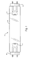
- FIG. 1 or FIG. 1a there is shown a representative discharge lamp 10, which is generally known in the art.
- the lamp 10 has a glass tube or light-transmissive envelope 12 which has a circular cross-section, and would include the conventional electrodes 14, fill gas 16, and mercury components (not shown) known in the art.
- the tube 12 is hermetically sealed at both ends by bases 18.
- the electrodes 14 are mounted in the bases 18, such that they sustain an arc discharge upon the application of power from a conventional lamp power source (not shown). Adjacent the base(s) 18 the lamp is configured to have a "pinch" area 20, where the quartz envelope diameter is constricted to provide support for the electrode assembly.
- FIG. 1a shows the foil 22 attached to electrode 14.
- All or any portion of the inner surface of the glass tube 12 may be coated with one or more coating layers (not shown), such as a transmissive barrier coating layer and/or a reflective barrier coating layer, of the type disclosed in U.S. Patent No. 5,602,444 , to our common assignee.
- a transmissive barrier coating layer and/or a reflective barrier coating layer of the type disclosed in U.S. Patent No. 5,602,444 , to our common assignee.
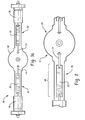
- FIG. 2 provides an expanded view of the pinch area 20 of a discharge lamp according to the invention. This corresponds to the type of lamp shown in FIG. 1a .
- foil 22 connects to electrode 14.
- the quartz envelope 12, while it is wider in region 24 representing the central portion of this type of lamp, is "pinched" in the area 26 of the electrode/foil connection, bringing the quartz into closer proximity with the electrode assembly than might otherwise be established.
- the pinch design is used to provide physical support for the electrode assembly.
- the coating comprises at least a Ni-Mo-Cr composite metal.
- This coating according to the invention is characterized by a high melting point and low diffusion distance.
- the term “diffusion distance” refers to the distance traveled by an atom of a material, here a coating material, before it is trapped by atoms of the material into which it is diffusing.
- the coating may comprise certain oxides, such as titanium oxide, zinc oxide, indium oxide, aluminum oxide, and composites such as TiInO, SrTiO, LaSrTiO 3 , CuAlS. It is important for the coating to be conducting so that it does not interfere with operation of the lamp.
- the coating may be doped to further enhance the performance thereof.
- Dopants may be selected from such materials as silicon, boron and carbon, which may be added as ions or in the elemental form by diffusing them into the coating composition at a very high temperature, after deposition of the coating.
- the coating of the invention comprises several layers.
- the first layer of the coating is deposited at a thickness of about at least about 4/5 of a nanometer. This deposition may be accomplished by any known deposition technique.
- the layer is deposited at a temperature of at least 400°C. Deposition at this temperature causes the barrier layer material to form a layer of nanoclusters of the material, as opposed to just a thin film of the nature deposited at lower temperatures, conventionally about 100°C.
- the thin layer of material deposited at this lower temperature undergoes at least partial diffusion of the metal of the coating into the metal foil.
- the metal coating material does not diffuse into the foil or coil material, but rather is deposited as a coating of ultra hard nanoclusters, characterized by the fact that once deposited they remain substantially as an ultra hard surface layer, even when exposed to high temperature.
- FIG. 3 sets forth a coated foil in cross section. It is seen in this figure that the first layer of the coating 28 resides on the surface of the metal foil in the form of the noted nanoclusters. In this figure, the second layer 30 is deposited in the form of a thin film corresponding to the oxide material referred to above. The coating further exhibits an interface 32 between the nanocluster layer and the thin film, and an interface 34 between the coating and the quartz envelope.
- the nanocluster coating layer comprises, for example Au, Ni, or Pt
- it can be deposited by sputtering. This deposition process is then followed by annealing at about 400°C for up to about 5 hours. The time necessary to deposit and anneal the coating is dependent on the coating thickness desired.
- the deposition temperature is determined by the metal content of the coating, i.e., metals with higher melting points require higher temperature deposition, or lower temperature deposition for a longer time period.
- the nanocluster coating layer is formed from, for example zinc, titanium oxide, indium oxide, or a sulfide or boride
- the layer can be deposited by conventional chemical vapor deposition techniques.
- chemical vapor deposition is the deposition of a high-purity, high-performance coating by exposing the surface to be coated, in this case the foil assembly, to one or more volatile coating precursors.
- Activation and process conditions vary depending on the type of process used to initiate the chemical reaction, for example: operating pressure CVD, including but not limited to atmospheric pressure CVD, low-pressure CVD, and the like; vapor CVD, including but not limited to aerosol CVD, liquid injection CVD, and the like; plasma enhanced CVD; atomic layer CVD; hot wire CVD; metal-organic CVD; and others.
- operating pressure CVD including but not limited to atmospheric pressure CVD, low-pressure CVD, and the like
- vapor CVD including but not limited to aerosol CVD, liquid injection CVD, and the like
- plasma enhanced CVD atomic layer CVD
- hot wire CVD hot wire CVD
- metal-organic CVD metal-organic CVD
- the invention further includes the addition to the foregoing oxide layers of a dopant.
- the oxide materials may be coated with a very thin layer of silicon, boron or carbon, for example, to further reduce the thermal expansion mismatch between the quartz envelope and the material most closely adjacent or proximate thereto.
- the size of the nanoclusters which comprise the coating described herein may vary. Generally, the clusters are larger as the layer of coating increases in thickness due to the fact that the clusters grow linearly with increased coating thickness.
- a second layer having a thickness of about 1500 nanometers is deposited.
- This secondary layer of the coating according to the invention may be formed from the same material as the initial layer, or may be formed from another metal composition.
- the entire coating, including the initial and secondary or additional layers, comprises Ni-Mo-Cr.
- a coating comprising a mixture of components, such as the Ni-Mo-Cr coating, may exhibit better resistance to stress due to the fact that the mixed coating is likely to be more granular. While a single component coating is sufficient to block oxidation of the foil/electrode assembly, it may not resolve problems related to stress as efficiently as a mixed coating layer.
- the coating may comprise an initial gold nanocluster layer, for example, followed by an indium oxide/zinc oxide secondary layer.
- either layer or both layers may be doped with, for example, silicon.
- an oxide containing material as the second layer of the coating, the coating can be made more susceptible to bonding of other materials.
- a nanocluster layer of metal such as gold
- a second layer comprising TiInO.
- this ordering of layers is not necessary and the layers may be deposited in any order, i.e. metal or oxide/carbide/nitride first followed by the other. Both layers may be deposited using the same deposition technique, or different deposition processing may be employed.
- the initial layer is preferably deposited as a nanocluster layer
- the secondary or subsequent coating layer or layers may be deposited as a thicker nanocluster layer or as a thin film layer of the stated approximate thickness. Even where the latter thin film construction is used, the initial nanocluster layer provides a barrier against coating metal diffusion into the metal coil.
- the multiple layer coating comprising at least the initial deposition layer and the secondary deposition layer as provided herein, not only addresses the problem of thermal mismatch between the quartz or other lamp envelope and the electrode/foil assembly, but further functions to reduce oxidation of the molybdenum foil.
- the coating layer is gold or platinum, because these metals do not oxidize, once the coating is deposited, there is no possibility that lamp failure will result from oxidative failure of the electrode assembly.
- the coating layer is alternatively comprised of, for example, zinc or indium oxide, or any other material already in the oxide state, further oxidation is not possible or only negligible.
- the inventive nanocluster coating including at least an initial nanocluster layer and a secondary layer, deposited onto the foil/coil assembly in the pinch area of the lamp protects the electrode and the foil/coil from oxidative failure, resulting in shortened lamp life. This is important, especially at higher operating temperatures, on the average of about 500°C to 600°C. At elevated temperatures in this range, oxidation of the foil/electrode assembly occurs faster due to molybdenum diffusion and oxidation.
- the surface of the foil Before deposition of the coating, the surface of the foil can be etched to exhibit a roughness of greater than 100nm. This etching process is used to enhance the adaptability of the foil to the quartz envelope. When the quartz envelope undergoes the pinch process, the quartz becomes soft and rough due to the temperature of the process. This creates two problems. First, the quartz is now rough in the area where it is being used to create a seal with the foil, which is smooth, making the creation of a good seal, which will completely control oxygen access to the electrode assembly, difficult. The second problem arises during lamp use as the quartz and foil experience thermal mismatch. Optimally, the foil would expand and contract with the quartz. Roughing the surface of the foil is one means to help avoid these problems.
- the coating herein addresses these issues by providing an enhanced seal between the foil and the quartz, and by providing enhanced slip.
- the non-oxidizing coating eliminates the possibility of the foil oxidizing. Further, the coating composition reduces the thermal mismatch between the foil and the quartz significantly.
- the nanocluster coating layer offers yet a further advantage.
- the coating may also function as a dampening spring. This occurs as the quartz envelope begins to absorb heat generated by lamp operation.
- the stress of the heat deposited in the pinch area of the lamp which in a conventional lamp lacking the nanocluster coating may result in envelope softening or electrode oxidative degradation, among other types of failure, is instead absorbed by the nanocluster coating layer. Absorption of this heat energy by the coating layer stabilizes the foil assembly, or provides a dampening effect with regard to the propagation of heat-generated degradation, thus stalling potential lamp failure.
- one or more additional layer(s) may be added during deposition of the coating.
- This additional layer or layers may have a thickness of up to about 5 nm. If added, this layer functions to provide further adaptability of the coating layer to the quartz, and can be formed of any of the oxides mentioned hereinabove and deposited by any known deposition technique.
- a lamp including a conventional molybdenum foil/electrode assembly was coated with a 10nm Ni/Au nanocluster layer, deposited by sputtering, and over-coated with a TiO 2 /Si oxide layer exhibiting a thickness of between 200-400nm.
- Deposition of both layers was conducted using a sputtering deposition process, conducted at 300-400°C.
- the molybdenum foil/electrode assembly was brought to a temperature of 200°C prior to the deposition of the coating and was maintained at this temperature until the doeposition chamber was evacuated, about 30 minutes after deposition.
- the coating was deposited at the rate of 2A/sec. During deposition the substrate was constantly rotated at an angle of greater than 30 degrees to ensure uniform but rough coverage.
- the coating process was completed, comparative testing was conducted in two manners.
- the coated molybdenum foil/electrode assembly and an identical electrode assembly but in the uncoated state were placed in an open air oven, the temperature of which was raised to 600°C. At this temperature, simulating elevated operating temperature, the molybdenum foil coated as set forth above in accord with the disclosure herein exhibited no oxidative degradation after more than 50 hours.
- the uncoated molybdenum foil failed after only 2 minutes at the elevated temperature, the failure being visually noticeable by the oxidation and cracking of the uncoated foil.
- the foils were subject to power cycling. Specifically, the foils, coated and uncoated, were subjected to 28 amp power, cycled through the foil at a rate of 30 cylces/day. This test regimen is comparable to operation of an actual lamp at 700°C for 300 hours. After only 20 cycles, the uncoated foil failed and could no longer support the applied charge. The coated foil, in contrast, continued to support the applied charge through the entire test period, at the end of which time the coated foil exhibited only slight and almost no visible sign of degradation. Upon examination it was confirmed that the uncoated foil had experienced degradation at the molybdenum-oxide envelope interface during the pinch process, as evidenced by the presence of stress risers. Figure 3 clearly shows the stress risers referred to.
- the coated electrode assembly when examined after 50 hours of testing showed no sign of stress risers.
- the foregoing results can be extrapolated to determine the effect the coating of the disclosure would have on the foil assembly during the pinch process and in operation.
- the results indicate the ability of the coating to remain adhesively bound to the foil assembly at operating temperatures in excess of 600°C. This is critical for use in certain lamp applications where elevated temperatures, in addition to accumulating heat energy cause lamps to fail early. This conclusion is supported by the lack of crack formation and oxidation on the coated assembly after testing. It is fully expected that the coating described herein will be suitable for use in any number of applications exhibiting potential for a thermal mismatch in a metal/ceramic system.
Landscapes
- Vessels And Coating Films For Discharge Lamps (AREA)
Priority Applications (1)
| Application Number | Priority Date | Filing Date | Title |
|---|---|---|---|
| PL08771296T PL2183763T3 (pl) | 2007-08-01 | 2008-06-18 | Zespół połączenia metalu z tlenkiem odporny na działanie wysokich temperatur roboczych i zmniejszający powstawania pęknięć |
Applications Claiming Priority (2)
| Application Number | Priority Date | Filing Date | Title |
|---|---|---|---|
| US11/832,230 US7863818B2 (en) | 2007-08-01 | 2007-08-01 | Coil/foil-electrode assembly to sustain high operating temperature and reduce shaling |
| PCT/US2008/067265 WO2009017891A1 (en) | 2007-08-01 | 2008-06-18 | Metal and oxide interface assembly to sustain high operating temperature and reduce shaling |
Publications (2)
| Publication Number | Publication Date |
|---|---|
| EP2183763A1 EP2183763A1 (en) | 2010-05-12 |
| EP2183763B1 true EP2183763B1 (en) | 2014-03-12 |
Family
ID=39739890
Family Applications (1)
| Application Number | Title | Priority Date | Filing Date |
|---|---|---|---|
| EP08771296.4A Not-in-force EP2183763B1 (en) | 2007-08-01 | 2008-06-18 | Metal and oxide interface assembly to sustain high operating temperature and reduce shaling |
Country Status (6)
| Country | Link |
|---|---|
| US (1) | US7863818B2 (enExample) |
| EP (1) | EP2183763B1 (enExample) |
| JP (1) | JP5400776B2 (enExample) |
| CN (1) | CN101772826B (enExample) |
| PL (1) | PL2183763T3 (enExample) |
| WO (1) | WO2009017891A1 (enExample) |
Families Citing this family (4)
| Publication number | Priority date | Publication date | Assignee | Title |
|---|---|---|---|---|
| US8035285B2 (en) * | 2009-07-08 | 2011-10-11 | General Electric Company | Hybrid interference coatings, lamps, and methods |
| US10529551B2 (en) * | 2012-11-26 | 2020-01-07 | Lucidity Lights, Inc. | Fast start fluorescent light bulb |
| DE102015218878A1 (de) * | 2015-09-30 | 2017-03-30 | Osram Gmbh | Gleichstrom-Gasentladungslampe mit einer thoriumfreien Kathode |
| US10236174B1 (en) | 2017-12-28 | 2019-03-19 | Lucidity Lights, Inc. | Lumen maintenance in fluorescent lamps |
Citations (1)
| Publication number | Priority date | Publication date | Assignee | Title |
|---|---|---|---|---|
| US20030052608A1 (en) * | 2001-09-12 | 2003-03-20 | Ushiodenki Kabushiki Kaisha | Discharge lamp |
Family Cites Families (21)
| Publication number | Priority date | Publication date | Assignee | Title |
|---|---|---|---|---|
| US2697130A (en) * | 1950-12-30 | 1954-12-14 | Westinghouse Electric Corp | Protection of metal against oxidation |
| NL106429C (nl) * | 1959-09-23 | 1963-11-15 | Philips Nv | Werkwijze ter vervaardiging van een elektrische lamp, alsmede volgens deze werkwijze vervaardigde elektrische lamp |
| US3420944A (en) * | 1966-09-02 | 1969-01-07 | Gen Electric | Lead-in conductor for electrical devices |
| DE3812084A1 (de) | 1988-04-12 | 1989-10-26 | Philips Patentverwaltung | Metallhalogenid-hochdruckgasentladungslampe |
| US5021711A (en) * | 1990-10-29 | 1991-06-04 | Gte Products Corporation | Quartz lamp envelope with molybdenum foil having oxidation-resistant surface formed by ion implantation |
| JPH11111240A (ja) * | 1997-09-30 | 1999-04-23 | Toshiba Lighting & Technology Corp | 封止用金属箔、管球および照明器具 |
| WO2000010193A1 (en) * | 1998-08-13 | 2000-02-24 | Koninklijke Philips Electronics N.V. | Electric lamp having a coated external current conductor |
| DE19915920A1 (de) * | 1999-04-09 | 2000-10-19 | Heraeus Gmbh W C | Metallisches Bauteil und Entladungslampe |
| JP2000315456A (ja) * | 1999-04-30 | 2000-11-14 | Matsushita Electric Ind Co Ltd | 放電型ランプとその製造方法 |
| DE60039657D1 (de) | 1999-07-02 | 2008-09-11 | Phoenix Electric Co Ltd | Aufbauanordnung für Lampe und Dichtungsstruktur einer Lampe mit einer solchen Aufbauanordnung |
| AT4408U1 (de) * | 2000-05-18 | 2001-06-25 | Plansee Ag | Verfahren zur herstellung einer elektrischen lampe |
| JP3648184B2 (ja) * | 2001-09-07 | 2005-05-18 | 株式会社小糸製作所 | 放電ランプアークチューブおよび同アークチューブの製造方法 |
| JP3543799B2 (ja) * | 2001-10-17 | 2004-07-21 | ウシオ電機株式会社 | ショートアーク型超高圧放電ランプ |
| JP2003317659A (ja) * | 2002-04-25 | 2003-11-07 | Ushio Inc | 放電ランプ |
| DE10245922A1 (de) * | 2002-10-02 | 2004-04-15 | Philips Intellectual Property & Standards Gmbh | Hochdruckgasentladungslampe |
| JP2004273358A (ja) * | 2003-03-11 | 2004-09-30 | Harison Toshiba Lighting Corp | ガラス封着用金属線および管球ならびに電気部品 |
| JP4196850B2 (ja) * | 2004-02-16 | 2008-12-17 | ウシオ電機株式会社 | 箔シールランプ |
| US7126266B2 (en) * | 2004-07-14 | 2006-10-24 | The Board Of Trustees Of The University Of Illinois | Field emission assisted microdischarge devices |
| JP2007012508A (ja) * | 2005-07-01 | 2007-01-18 | Ushio Inc | 放電ランプ |
| US7719194B2 (en) * | 2006-05-12 | 2010-05-18 | General Electric Company | Inhibited oxidation foil connector for a lamp |
| JP2008181680A (ja) * | 2007-01-23 | 2008-08-07 | Harison Toshiba Lighting Corp | メタルハライドランプ、点灯装置、自動車用前照灯装置 |
-
2007
- 2007-08-01 US US11/832,230 patent/US7863818B2/en not_active Expired - Fee Related
-
2008
- 2008-06-18 WO PCT/US2008/067265 patent/WO2009017891A1/en not_active Ceased
- 2008-06-18 EP EP08771296.4A patent/EP2183763B1/en not_active Not-in-force
- 2008-06-18 JP JP2010520018A patent/JP5400776B2/ja not_active Expired - Fee Related
- 2008-06-18 CN CN200880101424XA patent/CN101772826B/zh not_active Expired - Fee Related
- 2008-06-18 PL PL08771296T patent/PL2183763T3/pl unknown
Patent Citations (1)
| Publication number | Priority date | Publication date | Assignee | Title |
|---|---|---|---|---|
| US20030052608A1 (en) * | 2001-09-12 | 2003-03-20 | Ushiodenki Kabushiki Kaisha | Discharge lamp |
Also Published As
| Publication number | Publication date |
|---|---|
| PL2183763T3 (pl) | 2014-07-31 |
| US7863818B2 (en) | 2011-01-04 |
| CN101772826A (zh) | 2010-07-07 |
| US20090033200A1 (en) | 2009-02-05 |
| JP5400776B2 (ja) | 2014-01-29 |
| JP2010535401A (ja) | 2010-11-18 |
| WO2009017891A1 (en) | 2009-02-05 |
| EP2183763A1 (en) | 2010-05-12 |
| CN101772826B (zh) | 2013-04-24 |
Similar Documents
| Publication | Publication Date | Title |
|---|---|---|
| EP0895275B1 (en) | Tungsten halogen lamp and method for manufacturing the same | |
| US20080176479A1 (en) | Conductive element and method of making | |
| EP2183763B1 (en) | Metal and oxide interface assembly to sustain high operating temperature and reduce shaling | |
| US6456005B1 (en) | Materials and methods for application of conducting members on arc tubes | |
| CN100345245C (zh) | 具有光学干涉滤光器的电灯 | |
| JP2002033079A (ja) | 電灯の製造方法 | |
| EP2020019B1 (en) | Lamp with a foil connector | |
| CA2767356C (en) | Hybrid interference coatings, lamps, and methods | |
| US7772749B2 (en) | Wavelength filtering coating for high temperature lamps | |
| CN1717773A (zh) | 高压气体放电灯 | |
| WO2005029536A2 (en) | Electric lamp with an optical interference film | |
| TWI274366B (en) | Cathode with integrated getter and low work function for cold cathode lamps | |
| US7719192B2 (en) | Metal halide lamp with intermetal interface gradient | |
| JP3119264B2 (ja) | 傾斜機能材料製閉塞体を具えた管球 | |
| US20080036377A1 (en) | Light Bulb Comprising An Illumination Body That Contains Carbide | |
| WO2005073998A2 (en) | Compact high-pressure discharge lamp and method of manufacturing | |
| JP2023174123A (ja) | 放電ランプおよび放電ランプ用電極の製造方法 | |
| JP2009206098A (ja) | クロムをコーティングしたニオビウムフィードスルーを備えるセラミック製の放電容器及び該放電容器を収納する放電灯 |
Legal Events
| Date | Code | Title | Description |
|---|---|---|---|
| PUAI | Public reference made under article 153(3) epc to a published international application that has entered the european phase |
Free format text: ORIGINAL CODE: 0009012 |
|
| 17P | Request for examination filed |
Effective date: 20100301 |
|
| AK | Designated contracting states |
Kind code of ref document: A1 Designated state(s): AT BE BG CH CY CZ DE DK EE ES FI FR GB GR HR HU IE IS IT LI LT LU LV MC MT NL NO PL PT RO SE SI SK TR |
|
| AX | Request for extension of the european patent |
Extension state: AL BA MK RS |
|
| 17Q | First examination report despatched |
Effective date: 20100531 |
|
| DAX | Request for extension of the european patent (deleted) | ||
| GRAP | Despatch of communication of intention to grant a patent |
Free format text: ORIGINAL CODE: EPIDOSNIGR1 |
|
| INTG | Intention to grant announced |
Effective date: 20131023 |
|
| GRAS | Grant fee paid |
Free format text: ORIGINAL CODE: EPIDOSNIGR3 |
|
| GRAA | (expected) grant |
Free format text: ORIGINAL CODE: 0009210 |
|
| AK | Designated contracting states |
Kind code of ref document: B1 Designated state(s): AT BE BG CH CY CZ DE DK EE ES FI FR GB GR HR HU IE IS IT LI LT LU LV MC MT NL NO PL PT RO SE SI SK TR |
|
| REG | Reference to a national code |
Ref country code: GB Ref legal event code: FG4D |
|
| REG | Reference to a national code |
Ref country code: CH Ref legal event code: EP |
|
| REG | Reference to a national code |
Ref country code: AT Ref legal event code: REF Ref document number: 656788 Country of ref document: AT Kind code of ref document: T Effective date: 20140315 |
|
| REG | Reference to a national code |
Ref country code: IE Ref legal event code: FG4D |
|
| REG | Reference to a national code |
Ref country code: NL Ref legal event code: T3 |
|
| REG | Reference to a national code |
Ref country code: DE Ref legal event code: R096 Ref document number: 602008030849 Country of ref document: DE Effective date: 20140424 |
|
| PG25 | Lapsed in a contracting state [announced via postgrant information from national office to epo] |
Ref country code: LT Free format text: LAPSE BECAUSE OF FAILURE TO SUBMIT A TRANSLATION OF THE DESCRIPTION OR TO PAY THE FEE WITHIN THE PRESCRIBED TIME-LIMIT Effective date: 20140312 Ref country code: NO Free format text: LAPSE BECAUSE OF FAILURE TO SUBMIT A TRANSLATION OF THE DESCRIPTION OR TO PAY THE FEE WITHIN THE PRESCRIBED TIME-LIMIT Effective date: 20140612 |
|
| PGFP | Annual fee paid to national office [announced via postgrant information from national office to epo] |
Ref country code: GB Payment date: 20140627 Year of fee payment: 7 |
|
| REG | Reference to a national code |
Ref country code: PL Ref legal event code: T3 |
|
| REG | Reference to a national code |
Ref country code: AT Ref legal event code: MK05 Ref document number: 656788 Country of ref document: AT Kind code of ref document: T Effective date: 20140312 |
|
| REG | Reference to a national code |
Ref country code: LT Ref legal event code: MG4D |
|
| PG25 | Lapsed in a contracting state [announced via postgrant information from national office to epo] |
Ref country code: FI Free format text: LAPSE BECAUSE OF FAILURE TO SUBMIT A TRANSLATION OF THE DESCRIPTION OR TO PAY THE FEE WITHIN THE PRESCRIBED TIME-LIMIT Effective date: 20140312 Ref country code: CY Free format text: LAPSE BECAUSE OF FAILURE TO SUBMIT A TRANSLATION OF THE DESCRIPTION OR TO PAY THE FEE WITHIN THE PRESCRIBED TIME-LIMIT Effective date: 20140312 Ref country code: SE Free format text: LAPSE BECAUSE OF FAILURE TO SUBMIT A TRANSLATION OF THE DESCRIPTION OR TO PAY THE FEE WITHIN THE PRESCRIBED TIME-LIMIT Effective date: 20140312 |
|
| PG25 | Lapsed in a contracting state [announced via postgrant information from national office to epo] |
Ref country code: LV Free format text: LAPSE BECAUSE OF FAILURE TO SUBMIT A TRANSLATION OF THE DESCRIPTION OR TO PAY THE FEE WITHIN THE PRESCRIBED TIME-LIMIT Effective date: 20140312 Ref country code: HR Free format text: LAPSE BECAUSE OF FAILURE TO SUBMIT A TRANSLATION OF THE DESCRIPTION OR TO PAY THE FEE WITHIN THE PRESCRIBED TIME-LIMIT Effective date: 20140312 |
|
| PGFP | Annual fee paid to national office [announced via postgrant information from national office to epo] |
Ref country code: PL Payment date: 20140609 Year of fee payment: 7 |
|
| PG25 | Lapsed in a contracting state [announced via postgrant information from national office to epo] |
Ref country code: BE Free format text: LAPSE BECAUSE OF FAILURE TO SUBMIT A TRANSLATION OF THE DESCRIPTION OR TO PAY THE FEE WITHIN THE PRESCRIBED TIME-LIMIT Effective date: 20140312 Ref country code: CZ Free format text: LAPSE BECAUSE OF FAILURE TO SUBMIT A TRANSLATION OF THE DESCRIPTION OR TO PAY THE FEE WITHIN THE PRESCRIBED TIME-LIMIT Effective date: 20140312 Ref country code: EE Free format text: LAPSE BECAUSE OF FAILURE TO SUBMIT A TRANSLATION OF THE DESCRIPTION OR TO PAY THE FEE WITHIN THE PRESCRIBED TIME-LIMIT Effective date: 20140312 Ref country code: RO Free format text: LAPSE BECAUSE OF FAILURE TO SUBMIT A TRANSLATION OF THE DESCRIPTION OR TO PAY THE FEE WITHIN THE PRESCRIBED TIME-LIMIT Effective date: 20140312 Ref country code: IS Free format text: LAPSE BECAUSE OF FAILURE TO SUBMIT A TRANSLATION OF THE DESCRIPTION OR TO PAY THE FEE WITHIN THE PRESCRIBED TIME-LIMIT Effective date: 20140712 Ref country code: BG Free format text: LAPSE BECAUSE OF FAILURE TO SUBMIT A TRANSLATION OF THE DESCRIPTION OR TO PAY THE FEE WITHIN THE PRESCRIBED TIME-LIMIT Effective date: 20140612 |
|
| PGFP | Annual fee paid to national office [announced via postgrant information from national office to epo] |
Ref country code: NL Payment date: 20140626 Year of fee payment: 7 Ref country code: DE Payment date: 20140627 Year of fee payment: 7 |
|
| PG25 | Lapsed in a contracting state [announced via postgrant information from national office to epo] |
Ref country code: SK Free format text: LAPSE BECAUSE OF FAILURE TO SUBMIT A TRANSLATION OF THE DESCRIPTION OR TO PAY THE FEE WITHIN THE PRESCRIBED TIME-LIMIT Effective date: 20140312 Ref country code: AT Free format text: LAPSE BECAUSE OF FAILURE TO SUBMIT A TRANSLATION OF THE DESCRIPTION OR TO PAY THE FEE WITHIN THE PRESCRIBED TIME-LIMIT Effective date: 20140312 Ref country code: ES Free format text: LAPSE BECAUSE OF FAILURE TO SUBMIT A TRANSLATION OF THE DESCRIPTION OR TO PAY THE FEE WITHIN THE PRESCRIBED TIME-LIMIT Effective date: 20140312 |
|
| REG | Reference to a national code |
Ref country code: DE Ref legal event code: R097 Ref document number: 602008030849 Country of ref document: DE |
|
| PG25 | Lapsed in a contracting state [announced via postgrant information from national office to epo] |
Ref country code: PT Free format text: LAPSE BECAUSE OF FAILURE TO SUBMIT A TRANSLATION OF THE DESCRIPTION OR TO PAY THE FEE WITHIN THE PRESCRIBED TIME-LIMIT Effective date: 20140714 |
|
| PLBE | No opposition filed within time limit |
Free format text: ORIGINAL CODE: 0009261 |
|
| STAA | Information on the status of an ep patent application or granted ep patent |
Free format text: STATUS: NO OPPOSITION FILED WITHIN TIME LIMIT |
|
| PG25 | Lapsed in a contracting state [announced via postgrant information from national office to epo] |
Ref country code: DK Free format text: LAPSE BECAUSE OF FAILURE TO SUBMIT A TRANSLATION OF THE DESCRIPTION OR TO PAY THE FEE WITHIN THE PRESCRIBED TIME-LIMIT Effective date: 20140312 Ref country code: MC Free format text: LAPSE BECAUSE OF FAILURE TO SUBMIT A TRANSLATION OF THE DESCRIPTION OR TO PAY THE FEE WITHIN THE PRESCRIBED TIME-LIMIT Effective date: 20140312 Ref country code: LU Free format text: LAPSE BECAUSE OF FAILURE TO SUBMIT A TRANSLATION OF THE DESCRIPTION OR TO PAY THE FEE WITHIN THE PRESCRIBED TIME-LIMIT Effective date: 20140618 |
|
| REG | Reference to a national code |
Ref country code: CH Ref legal event code: PL |
|
| 26N | No opposition filed |
Effective date: 20141215 |
|
| REG | Reference to a national code |
Ref country code: IE Ref legal event code: MM4A |
|
| REG | Reference to a national code |
Ref country code: DE Ref legal event code: R097 Ref document number: 602008030849 Country of ref document: DE Effective date: 20141215 |
|
| REG | Reference to a national code |
Ref country code: FR Ref legal event code: ST Effective date: 20150227 |
|
| PG25 | Lapsed in a contracting state [announced via postgrant information from national office to epo] |
Ref country code: IT Free format text: LAPSE BECAUSE OF FAILURE TO SUBMIT A TRANSLATION OF THE DESCRIPTION OR TO PAY THE FEE WITHIN THE PRESCRIBED TIME-LIMIT Effective date: 20140312 |
|
| PG25 | Lapsed in a contracting state [announced via postgrant information from national office to epo] |
Ref country code: IE Free format text: LAPSE BECAUSE OF NON-PAYMENT OF DUE FEES Effective date: 20140618 Ref country code: CH Free format text: LAPSE BECAUSE OF NON-PAYMENT OF DUE FEES Effective date: 20140630 Ref country code: LI Free format text: LAPSE BECAUSE OF NON-PAYMENT OF DUE FEES Effective date: 20140630 |
|
| PG25 | Lapsed in a contracting state [announced via postgrant information from national office to epo] |
Ref country code: FR Free format text: LAPSE BECAUSE OF NON-PAYMENT OF DUE FEES Effective date: 20140630 |
|
| PG25 | Lapsed in a contracting state [announced via postgrant information from national office to epo] |
Ref country code: SI Free format text: LAPSE BECAUSE OF FAILURE TO SUBMIT A TRANSLATION OF THE DESCRIPTION OR TO PAY THE FEE WITHIN THE PRESCRIBED TIME-LIMIT Effective date: 20140312 |
|
| REG | Reference to a national code |
Ref country code: DE Ref legal event code: R119 Ref document number: 602008030849 Country of ref document: DE |
|
| GBPC | Gb: european patent ceased through non-payment of renewal fee |
Effective date: 20150618 |
|
| REG | Reference to a national code |
Ref country code: NL Ref legal event code: MM Effective date: 20150701 |
|
| PG25 | Lapsed in a contracting state [announced via postgrant information from national office to epo] |
Ref country code: MT Free format text: LAPSE BECAUSE OF FAILURE TO SUBMIT A TRANSLATION OF THE DESCRIPTION OR TO PAY THE FEE WITHIN THE PRESCRIBED TIME-LIMIT Effective date: 20140312 |
|
| PG25 | Lapsed in a contracting state [announced via postgrant information from national office to epo] |
Ref country code: NL Free format text: LAPSE BECAUSE OF NON-PAYMENT OF DUE FEES Effective date: 20150701 Ref country code: DE Free format text: LAPSE BECAUSE OF NON-PAYMENT OF DUE FEES Effective date: 20160101 Ref country code: GB Free format text: LAPSE BECAUSE OF NON-PAYMENT OF DUE FEES Effective date: 20150618 |
|
| PG25 | Lapsed in a contracting state [announced via postgrant information from national office to epo] |
Ref country code: GR Free format text: LAPSE BECAUSE OF FAILURE TO SUBMIT A TRANSLATION OF THE DESCRIPTION OR TO PAY THE FEE WITHIN THE PRESCRIBED TIME-LIMIT Effective date: 20140613 |
|
| PG25 | Lapsed in a contracting state [announced via postgrant information from national office to epo] |
Ref country code: HU Free format text: LAPSE BECAUSE OF FAILURE TO SUBMIT A TRANSLATION OF THE DESCRIPTION OR TO PAY THE FEE WITHIN THE PRESCRIBED TIME-LIMIT; INVALID AB INITIO Effective date: 20080618 Ref country code: TR Free format text: LAPSE BECAUSE OF FAILURE TO SUBMIT A TRANSLATION OF THE DESCRIPTION OR TO PAY THE FEE WITHIN THE PRESCRIBED TIME-LIMIT Effective date: 20140312 |
|
| PG25 | Lapsed in a contracting state [announced via postgrant information from national office to epo] |
Ref country code: PL Free format text: LAPSE BECAUSE OF NON-PAYMENT OF DUE FEES Effective date: 20150618 |