EP2175251B1 - Spectroscope - Google Patents
Spectroscope Download PDFInfo
- Publication number
- EP2175251B1 EP2175251B1 EP08791860.3A EP08791860A EP2175251B1 EP 2175251 B1 EP2175251 B1 EP 2175251B1 EP 08791860 A EP08791860 A EP 08791860A EP 2175251 B1 EP2175251 B1 EP 2175251B1
- Authority
- EP
- European Patent Office
- Prior art keywords
- light
- prism
- beam deflector
- output
- wavelength
- Prior art date
- Legal status (The legal status is an assumption and is not a legal conclusion. Google has not performed a legal analysis and makes no representation as to the accuracy of the status listed.)
- Active
Links
- 239000013078 crystal Substances 0.000 claims description 101
- 230000003287 optical effect Effects 0.000 claims description 84
- 238000001514 detection method Methods 0.000 claims description 44
- 230000005684 electric field Effects 0.000 claims description 31
- 230000000694 effects Effects 0.000 claims description 29
- 230000010287 polarization Effects 0.000 claims description 13
- 239000000203 mixture Substances 0.000 claims description 3
- 230000008859 change Effects 0.000 description 36
- 238000005259 measurement Methods 0.000 description 32
- 239000006185 dispersion Substances 0.000 description 30
- 238000010586 diagram Methods 0.000 description 27
- 230000023077 detection of light stimulus Effects 0.000 description 19
- 230000004044 response Effects 0.000 description 17
- 239000011521 glass Substances 0.000 description 13
- 238000004611 spectroscopical analysis Methods 0.000 description 11
- 239000000463 material Substances 0.000 description 10
- 238000010408 sweeping Methods 0.000 description 6
- -1 LiIO3 Inorganic materials 0.000 description 4
- 239000002612 dispersion medium Substances 0.000 description 4
- 230000000644 propagated effect Effects 0.000 description 4
- 230000009467 reduction Effects 0.000 description 4
- 230000035945 sensitivity Effects 0.000 description 4
- 230000014509 gene expression Effects 0.000 description 3
- 230000007246 mechanism Effects 0.000 description 3
- 239000002609 medium Substances 0.000 description 3
- 229910019695 Nb2O6 Inorganic materials 0.000 description 2
- 230000005540 biological transmission Effects 0.000 description 2
- 230000000875 corresponding effect Effects 0.000 description 2
- 230000006872 improvement Effects 0.000 description 2
- 238000000034 method Methods 0.000 description 2
- 230000008569 process Effects 0.000 description 2
- 238000012545 processing Methods 0.000 description 2
- 238000007740 vapor deposition Methods 0.000 description 2
- 229910019670 (NH4)H2PO4 Inorganic materials 0.000 description 1
- 229910004613 CdTe Inorganic materials 0.000 description 1
- 229910005540 GaP Inorganic materials 0.000 description 1
- 229910001218 Gallium arsenide Inorganic materials 0.000 description 1
- 239000007836 KH2PO4 Substances 0.000 description 1
- 229910003334 KNbO3 Inorganic materials 0.000 description 1
- 229910013321 LiB3O5 Inorganic materials 0.000 description 1
- 229910003327 LiNbO3 Inorganic materials 0.000 description 1
- 229910012463 LiTaO3 Inorganic materials 0.000 description 1
- 229910020215 Pb(Mg1/3Nb2/3)O3PbTiO3 Inorganic materials 0.000 description 1
- 229910002370 SrTiO3 Inorganic materials 0.000 description 1
- 229910010252 TiO3 Inorganic materials 0.000 description 1
- 229910007709 ZnTe Inorganic materials 0.000 description 1
- 238000000862 absorption spectrum Methods 0.000 description 1
- 230000002411 adverse Effects 0.000 description 1
- 230000003466 anti-cipated effect Effects 0.000 description 1
- 229910002113 barium titanate Inorganic materials 0.000 description 1
- UHYPYGJEEGLRJD-UHFFFAOYSA-N cadmium(2+);selenium(2-) Chemical compound [Se-2].[Cd+2] UHYPYGJEEGLRJD-UHFFFAOYSA-N 0.000 description 1
- 238000004891 communication Methods 0.000 description 1
- 239000012141 concentrate Substances 0.000 description 1
- 230000001276 controlling effect Effects 0.000 description 1
- 238000007796 conventional method Methods 0.000 description 1
- 230000002596 correlated effect Effects 0.000 description 1
- 230000007547 defect Effects 0.000 description 1
- 230000000593 degrading effect Effects 0.000 description 1
- 230000001419 dependent effect Effects 0.000 description 1
- 238000011161 development Methods 0.000 description 1
- 230000018109 developmental process Effects 0.000 description 1
- 230000005611 electricity Effects 0.000 description 1
- 238000002189 fluorescence spectrum Methods 0.000 description 1
- 238000003754 machining Methods 0.000 description 1
- 229910000402 monopotassium phosphate Inorganic materials 0.000 description 1
- 230000010363 phase shift Effects 0.000 description 1
- GNSKLFRGEWLPPA-UHFFFAOYSA-M potassium dihydrogen phosphate Chemical compound [K+].OP(O)([O-])=O GNSKLFRGEWLPPA-UHFFFAOYSA-M 0.000 description 1
- 230000001902 propagating effect Effects 0.000 description 1
- SBIBMFFZSBJNJF-UHFFFAOYSA-N selenium;zinc Chemical compound [Se]=[Zn] SBIBMFFZSBJNJF-UHFFFAOYSA-N 0.000 description 1
- 238000007493 shaping process Methods 0.000 description 1
- 230000003595 spectral effect Effects 0.000 description 1
- 229910052950 sphalerite Inorganic materials 0.000 description 1
- 239000000126 substance Substances 0.000 description 1
- 238000011144 upstream manufacturing Methods 0.000 description 1
- 229910052984 zinc sulfide Inorganic materials 0.000 description 1
Images


Classifications
-
- G—PHYSICS
- G01—MEASURING; TESTING
- G01J—MEASUREMENT OF INTENSITY, VELOCITY, SPECTRAL CONTENT, POLARISATION, PHASE OR PULSE CHARACTERISTICS OF INFRARED, VISIBLE OR ULTRAVIOLET LIGHT; COLORIMETRY; RADIATION PYROMETRY
- G01J3/00—Spectrometry; Spectrophotometry; Monochromators; Measuring colours
- G01J3/12—Generating the spectrum; Monochromators
- G01J3/14—Generating the spectrum; Monochromators using refracting elements, e.g. prisms
-
- G—PHYSICS
- G01—MEASURING; TESTING
- G01J—MEASUREMENT OF INTENSITY, VELOCITY, SPECTRAL CONTENT, POLARISATION, PHASE OR PULSE CHARACTERISTICS OF INFRARED, VISIBLE OR ULTRAVIOLET LIGHT; COLORIMETRY; RADIATION PYROMETRY
- G01J3/00—Spectrometry; Spectrophotometry; Monochromators; Measuring colours
- G01J3/02—Details
- G01J3/0205—Optical elements not provided otherwise, e.g. optical manifolds, diffusers, windows
- G01J3/0237—Adjustable, e.g. focussing
-
- G—PHYSICS
- G01—MEASURING; TESTING
- G01J—MEASUREMENT OF INTENSITY, VELOCITY, SPECTRAL CONTENT, POLARISATION, PHASE OR PULSE CHARACTERISTICS OF INFRARED, VISIBLE OR ULTRAVIOLET LIGHT; COLORIMETRY; RADIATION PYROMETRY
- G01J3/00—Spectrometry; Spectrophotometry; Monochromators; Measuring colours
- G01J3/02—Details
- G01J3/06—Scanning arrangements arrangements for order-selection
-
- G—PHYSICS
- G01—MEASURING; TESTING
- G01J—MEASUREMENT OF INTENSITY, VELOCITY, SPECTRAL CONTENT, POLARISATION, PHASE OR PULSE CHARACTERISTICS OF INFRARED, VISIBLE OR ULTRAVIOLET LIGHT; COLORIMETRY; RADIATION PYROMETRY
- G01J3/00—Spectrometry; Spectrophotometry; Monochromators; Measuring colours
- G01J3/12—Generating the spectrum; Monochromators
- G01J3/18—Generating the spectrum; Monochromators using diffraction elements, e.g. grating
-
- G—PHYSICS
- G01—MEASURING; TESTING
- G01J—MEASUREMENT OF INTENSITY, VELOCITY, SPECTRAL CONTENT, POLARISATION, PHASE OR PULSE CHARACTERISTICS OF INFRARED, VISIBLE OR ULTRAVIOLET LIGHT; COLORIMETRY; RADIATION PYROMETRY
- G01J3/00—Spectrometry; Spectrophotometry; Monochromators; Measuring colours
- G01J3/28—Investigating the spectrum
- G01J3/30—Measuring the intensity of spectral lines directly on the spectrum itself
- G01J3/36—Investigating two or more bands of a spectrum by separate detectors
-
- G—PHYSICS
- G01—MEASURING; TESTING
- G01J—MEASUREMENT OF INTENSITY, VELOCITY, SPECTRAL CONTENT, POLARISATION, PHASE OR PULSE CHARACTERISTICS OF INFRARED, VISIBLE OR ULTRAVIOLET LIGHT; COLORIMETRY; RADIATION PYROMETRY
- G01J3/00—Spectrometry; Spectrophotometry; Monochromators; Measuring colours
- G01J3/02—Details
- G01J3/06—Scanning arrangements arrangements for order-selection
- G01J2003/064—Use of other elements for scan, e.g. mirror, fixed grating
Definitions
- the present invention relates to a spectroscope, and more particularly to a spectroscope for selecting an optical signal having an arbitrary wavelength.
- a spectroscope is employed for a device for measuring spectral characteristics of substances, such as absorption spectrums and fluorescence spectrums (see non-patent document 1).
- This spectroscope 100 includes a prism 101, which serves as spectroscopic means, a slit plate 102, which serves as wavelength selection means, and a photodetector 103.
- This spectroscope 200 includes a diffraction grating 201, which serves as spectroscopic means, a slit plate 202, which serve as wavelength selection means, and a photodetector 203.
- wavelength dispersion elements such as the prism 101 and the diffraction grating 201
- input light is spatially dispersed in directions that differ for individual wavelengths. From the dispersed light, only one portion is extracted by the wavelength selection means, and thus, light having a specified wavelength can be obtained.
- the prism 101 or the diffraction grating 201 is mechanically rotated, an arbitrary wavelength to be extracted can be selected.
- An arrayed waveguide grating 301 includes an input slab waveguide 303, connected to an input waveguide 302, an output slab waveguide 306, connected to an output waveguide 307, and arrayed waveguides 304, which connect the input slab waveguide 303 and the output slab waveguide 306.
- a specific length difference between adjacent waveguides is employed for the arrayed waveguides 304, and heaters 305a and 305b are relatively positioned for the individual waveguides.
- An optical signal received at the input waveguide 302 is transmitted, via the input slab waveguide 303, and distributed to the arrayed waveguides 304.
- the optical signal On the plane of incidence for the output slab waveguide 306, the optical signal is allocated for a different phase that is consonant with the wavelength of the signal. Since the output slab waveguide 306 serves as a collective lens, at the boundary between the output slab waveguide 306 and the output waveguide 307, the optical signal is collected at a different location in accordance with its wavelength. Therefore, only an optical signal having a specified wavelength, which has been collected at the boundary between the output slab waveguide 306 and the output waveguide 307, is output through the output waveguide 307.
- a current is supplied to the heater 305a or 305b, arranged along the arrayed waveguides 304, and a thermo-optic effect is employed to change the equivalent refractive index of the arrayed waveguides 304.
- the equivalent refractive index has been changed, the phases of optical signals passing through the arrayed waveguides 304 are shifted. Therefore, when a phase shift is controlled, only an optical signal having an arbitrary wavelength will be output through the output waveguide 307.
- Non-patent Document " The Physics of Light", Kohji Kushida, Published by Kyoritsu Shuppan Co. Ltd., First edition, Eighth impression, April 15, 1993 .
- the conventional spectroscopes in Figs. 1 and 2 must include a mechanical control unit, such as a motor for mechanically rotating either a prism or a diffraction grating, whichever serves as the spectroscopic means, and a drive circuit for driving the motor, and that the structure of the spectroscopes is increased.
- a mechanical control unit such as a motor for mechanically rotating either a prism or a diffraction grating, whichever serves as the spectroscopic means
- a drive circuit for driving the motor and that the structure of the spectroscopes is increased.
- this operation is performed mechanically, the response time required for varying a wavelength is long, and several ms are required.
- thermo-optic effect a large amount of electricity must be supplied to the heaters in order to produce the thermo-optic effect. Since a heat control mechanism is also required to supply the electric power and to cope with the heat that is generated, another problem is that downsizing of the device can not be attained. Furthermore, another defect is that the response time for varying a wavelength is long, i.e., 2 to 60 ms, because the thermo-optic effect is employed.
- Document JP 08159867 A discloses a light-waveform measuring apparatus. After the intensity is modulated by a light-modulating means, pulse light to be measured is made incident on a light deflecting means and swept for a prescribed duration. The intensity of the pulse light to be measured is lowered during the time except the sweeping time by modulation of the light-modulating means. Consequently, the intensity of the pulse light which is incident on a light detecting means is lowered during the time except the sweeping time. Scarce light to be measured can be transmitted through a slit during the period except the sweeping time by sufficiently lowering the light to be measured during the time except sweeping time.
- Document JP 2004 286582 discloses an electric field detection optical device and transceiver.
- the electric field detection optical device detects the electric field on the basis of the entered laser beam for detecting the electric field.
- An electric field detection optical part is mounted between a detected light output part and an entrance face of an electric-optic crystal, and comprises: a first cylindrical lens for focusing the laser beam in the facing direction of a signal electrode and a ground electrode and applying the laser beam to the entrance face of the electric-optic crystal member; and a second cylindrical lens mounted on an optical path of the laser beam in a state of being separated from an output face of the electric-optic crystal, and outputting the laser beam output from the output face of the electric-optical crystal as the parallel beam.
- a spectroscope comprising: a beam deflector that includes an electro-optic crystal, having an electro-optic effect, and paired electrodes used to apply an electric field inside the electro-optic crystal; spectroscopic means for dispersing light output by the beam deflector; and wavelength selection means for selecting light having an arbitrary wavelength from the light dispersed and output by the spectroscopic means.
- the beam deflector which includes the electro-optic crystal having an electro-optic effect, the spectroscopic means and the wavelength selection means are prepared, a short response time and downsizing of the device can be provided.
- the opening in the beam deflector is enlarged for the purpose of increasing the sensitivity of the spectroscope, in addition to a reduction in the response time and in the size of the spectroscope. That is, according to this aspect, the spectroscope is further configured that the width of the beam deflector is greater than the thickness of the beam deflector. Furthermore, the spectroscope of this aspect may further include means for projecting, to the beam deflector, light having an elliptic shape, in cross section. In this instance, the light having the elliptic shape, in cross section, enters the beam deflector, so that a direction along the long axis of the elliptic shape matches the direction of the width.
- the objective of a further aspect is that only a single operation is required to perform both a high resolution measurement and a wideband measurement, at the same time, and to employ both a low-dispersion prism and a high-dispersion prism as spectroscopic means. That is, for this aspect, the spectroscope is arranged such that: the spectroscopic means includes a first prism and a second prism for which refractive index dispersion is greater than that of the first prism; dividing means for outputting, in two different directions, light that is input, is further prepared; and the light output in the two different directions enter the first prism and the second prism.
- the dividing means may be arranged after the beam deflector and before the first and second prisms. Further, the dividing means may also output, in the two different directions, the light that is output by the beam deflector.
- the dividing means may be located in front of the beam deflector, and the light output in the two different directions may enter different areas in the beam deflector, and be transmitted to the first and the second prisms.
- the beam deflector may also include a first beam deflector and a second beam deflector, and the dividing means may be located in front of the first and the second beam deflectors, and the light output in the two different directions may enter the first and the second beam deflector and be transmitted to the first and the second prisms.
- the wavelength selection means may include first wavelength selection means, located at the rear of the first prism, and second wavelength selection means, located at the rear of the second prism, and the second wavelength means may be movable.
- the objective of a still further aspect is to provide a simple, high-resolution spectroscope, and at least one of either the input end or the output end of an electro-optic crystal, included in spectroscopic means, is wedge shaped.
- a spectroscope comprises: spectroscopic means, which includes an electro-optic crystal having an electro-optic effect and paired electrodes, used to apply an electric field inside the electro-optic crystal, and at the least, either an input end or an output end that is wedge shaped, so that the thickness of the end is gradually reduced from a first face, on which a first electrode of the paired electrodes is located, toward a second face, opposite the first face, on which a second electrode, of the paired electrodes, is located; and wavelength selection means for selecting light having an arbitrary wavelength from light that is dispersed and output by the spectroscopic means.
- the objectives of a further aspect are the acquisition of a high resolution without increasing the angle of the deflection of light that is output by a beam deflector, which includes an electro-optic crystal having an electro-optic effect, and a reduction in a required voltage that is to be applied to the beam deflector to obtain a predetermined resolution.
- a difference in optical path lengths is increased between a beam deflector and spectroscopic means, such as a prism or a diffraction grating.
- the spectroscope is arranged such that: a first input position denotes a position at which light output by the beam deflector enters the spectroscopic means when a first voltage is applied to the paired electrodes; a second input position denotes a position at which light output by the beam deflector enters the spectroscopic means when a second voltage is applied to the paired electrodes; a first output position denotes a position at which light is output from the spectroscopic means when the first voltage is applied to the paired electrodes; a second output position denotes a position at which light is output from the spectroscopic means when the second voltage is applied to the paired electrodes; and in a case wherein a voltage to be applied to the paired electrodes is changed from the first voltage to the second voltage, an output shift from the first output position to the second output position is greater than an incidence shift from the first input position to the second input position.
- a first angle may denote an angle formed, upon application of a third voltage to the paired electrodes, between the output plane of the spectroscopic means and the optical axis of light, having the shortest wavelength in a desired wavelength range for detection, that is included in light output by the beam deflector and that is output through the output plane of the spectroscopic means when the first electric field is applied for the detection of the shortest wavelength in the desired wavelength range
- a second angle may denote an angle that is formed, upon application of the fourth voltage to the paired electrodes, between the output plane of the spectroscopic means and the optical axis of light, having the longest wavelength in a desired wavelength range for detection, that is output through the output plane of the spectroscopic means when a second electric field is applied for the detection of light having the longest wavelength in the desired wavelength range.
- the first voltage and the second voltage may be set so that the second angle is greater than the first angle.
- the spectroscopic means may be a prism.
- a third input position denotes a position at which light output by the beam deflector enters the prism when the third voltage is applied to the paired electrodes for the detection of light having the shortest wavelength in a desired wavelength range
- a fourth input position denotes a position at which the light output by the beam deflector enters the prism when a fourth voltage is applied to the paired electrodes for the detection of the longest wavelength in the desired wavelength range
- a third output position denotes a position at which light from the prism is output when the third voltage is applied to the paired electrodes
- a fourth output position denotes a position at which light from the prism is output when a fourth voltage is applied to the paired electrodes
- ⁇ denotes an angle that is formed between the optical axis of light output by the beam deflector and the incidence plane of the prism when the third voltage is applied
- ⁇ denotes the angle of deflection of light output by the
- the optical path length difference L may be set for the beam deflector and the prism, so that a difference between F2 and F1,(F2 - F1), is a predetermined value.
- the spectroscope may further include a polarizer for projecting, onto the beam deflector, light consisting of only a component along a polarization axis, which is parallel to the electric field.
- the spectroscopic means is a prism.
- either the input end or the output end of the beam deflector may be wedge shaped, so that a thickness of the end is gradually reduced from the first face, where the first electrode of the paired electrodes is located, toward the second face, opposite the first face, where the second electrode of the paired electrodes is located.
- the wavelength selection means may be a slit plate.
- the electro-optic crystal is one of, KTa 1-x Nb x O 3 , K 1-y Li y Ta 1-x Nb x O 3 (0 ⁇ x ⁇ 1, 0 ⁇ y ⁇ 1).
- the beam deflector which includes an electro-optic crystal having an electro-optic effect
- the spectroscopic means and the wavelength selection means are prepared, a short response time and downsizing of the device can be obtained.
- the objective of the present invention is to provide a spectroscope for which the response time and the device size can be reduced, when compared with a conventional one.
- a beam deflector that deflects incident light, using an electro-optic crystal having an electro-optic effect, and outputs the deflected light is located upstream of a prism or a diffraction grating, which serves as spectroscopic means, in a direction in which dispersed light advances.
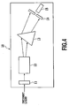
- Fig. 4 is a diagram illustrating the structure of a spectroscope having such an arrangement.
- a spectroscope 10 includes a polarizer 11 that polarizes incident light, a beam deflector 12 formed of a crystal having an electro-optic effect, a prism 13 that serves as spectroscopic means, a slit plate 14 that serves as wavelength selection means, and a photodetector 15.
- Example crystals having a large electro-optic constant are the following electro-optic crystals: KTaO 3 , KTa 1-x Nb x O 3 (0 ⁇ x1, hereinafter referred to as KTN), K 1-y Li y Ta 1-x Nb x O 3 (0 ⁇ x ⁇ 1, 0 ⁇ y ⁇ 1), LiNbO 3 , LiTaO 3 , LiIO 3 , KNbO 3 , KTiOPO 4 , BaTiO 3 , SrTiO 3 , Ba 1-x Sr x TiO 3 (0 ⁇ x ⁇ 1), Ba 1-x Sr x Nb 2 O 6 (0 ⁇ x ⁇ 1), Sr 0 . 75 Ba 0 .
- Ti/Pt/Au indicates that Pt and Au are laminated, in this order, on the lowermost Ti layer.
- the KTN crystal 21 is 6 mm long (z-axis), 4 mm wide (y-axis) and 0.5 mm thick (x-axis).
- the electrodes 22 and 23, arranged respectively on the upper and lower faces by vapor deposition, are 5 mm long along the z-axis.
- the positive electrode 22 is located on the upper face and the negative electrode 23 is located on the lower face; however, these electrodes may be inverted, or a power source that can switch polarities may be connected to them.
- the polarizer 11 for example, polarizes incident light, and transmits, to the KTN crystal 21, the resultant light of only a component that propagates along the polarization axis (x-axis) that is parallel to the electric field.
- the easy axis of transmission for the polarizer 11 is defined as a direction (x-axis) parallel to the electric field that is formed by the electrodes 22 and 23; however, the easy axis is not limited to this direction.
- the easy axis of transmission may be designated as a direction (y-axis) perpendicular to the direction parallel to the electric field, or a direction at an arbitrary angle relative to the direction parallel to the electric field. Or, the polarizer 11 may not be located.
- the importance of the embodiment of the present invention is that, as will be described later, light output by the beam deflector 12 should be deflected in accordance with the state under which a voltage is applied to the KTN crystal 21.
- the electric field is inclined by applying a voltage, and light that enters the KTN crystal 21 is deflected, although the degree of deflection varies, depending on the polarization state of the light that enters the KTN crystal 21. Therefore, an arbitrary polarization state is employed for the light that enters the KTN crystal 21.
- the polarizer 11 is located as shown in Fig. 4 , and only the component of the incident light propagating along the polarization axis (x-axis), which is parallel to the electric field, enters the KTN crystal 21.
- the gradient electric field inside the electro-optic crystal causes inclination in a change of a refractive index, which is provided by the electro-optic effect on the plane perpendicular to the optical axis of the incident beam. That is, the refractive index is inclined in accordance with the inclination of the electric field. Accordingly, when the refractive index is inclined, a gradient distribution is formed for the light velocity on the plane perpendicular to the axis of the light beam. As a result, during the propagation of light through the crystal, the direction traveled by the light is sequentially changed in accordance with the inclination of the refractive index, and deflection angles are accumulated.
- the deflection angle ⁇ of light output by the beam deflector 12 is a maximum of 125 mrad, relative to the application of a voltage of +250 V, or a maximum of -125 mrad, relative to the application of a voltage of -250 V. That is, in total, a deflection angle of close to 250 mrad can be obtained.
- the beam deflector 12 is employed to change the incidence angle of the prism 13 that serves as spectroscopic means, and a spectroscope that has a short response time can be provided. Furthermore, a mechanical control system is not required for the spectroscope, and the size of the device can be reduced. Since simply the application of the electric field is required for the KTN crystal 21, the consumption of current is low, and a thermal control mechanism is also not necessary. Furthermore, the response time for the beam deflector 12 is a period on the order of microseconds, and can be shorter by about three digits than that of a conventional spectroscope.
- a prism 13 is made, for example, of BK7 glass and is 15 mm long on a side used for transmitting light, and its apex a is 60 degrees.
- the length of an optical path extended from the beam deflector 12 to the prism 13 is 20 mm. It should be noted that the length of the optical path can be shortened by using a smaller prism 13.
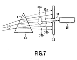
- reference numeral 31 denotes light having a wavelength that is selected from the incident light, and that passes through the slit plate 14.
- Reference numeral 32a denotes a light signal having a wavelength of 400 nm when an applied voltage is -55 V
- reference numeral 33a denotes a light signal having a wavelength of 700 nm when an applied voltage is -55 V
- reference numeral 32b denotes a light signal having a wavelength of 400 nm when an applied voltage is +55 V
- reference numeral 33b denotes a light signal having a wavelength of 700 nm when an applied voltage is +55 V.
- Fig. 7 assume that the wavelength range of incident light is 400 nm to 700 nm.
- the prism 13 is located so that when the voltage applied to the beam deflector 12 is +55 V, the light is input to the prism 13 at an incidence angle of 40 degrees, and the light signal 33b, which has a wavelength of 700 nm, is to pass through the slit plate 14 and be detected by the photodetector 15.
- the light output by the beam deflector 12 is dispersed by the prism 13 to light signals 32 and 33, in accordance with their wavelengths. Therefore, when a voltage applied to the beam deflector 12 is adjusted, the wavelength of the light passing through the slit plate 14 can be selected from the incident light.
- the angle of incidence for the prism 13 is changed from 40 degrees to 42 degrees by changing a voltage applied to the beam deflector 12 from +55 V to -55 V.
- Light signals covering the light signal 33b having a wavelength of 700 nm and the light signal 32b having a wavelength of 400 nm, can pass through the slit plate 14 and be detected by the photodetector 15. At this time, a period on the order of microseconds is required to sweep through the wavelength range of 700 nm to 400 nm.
- the width of the slit in the slit plate 14 is 200 ⁇ m.
- Wavelength resolution depends on a beam divergence angle, wavelength dispersion of the refractive index of a prism material, the incidence angle for the prism 13 and the distance between the prism 13 and the slit plate 14.
- the beam diameter of the beam deflector 12 is 400 ⁇ m
- the prism material is BK7
- the incidence angle for the prism 13 is 40 degrees
- the distance from the prism 13 to the slit plate 14 is 130 mm.
- the wavelength resolution at this time is about 4 nm, near a wavelength of 400 nm, or about 35 nm, near a wavelength of 700 nm.
- Table 1 shows a condition for the minimum angle of deviation when 550 nm is the central wavelength of incident light and a difference in the angle of refraction between a wavelength of 700 nm and a wavelength of 400 nm.
- the difference in the refraction angle is present because wavelength dependence of the refractive index differs for individual materials used for a prism.
- a difference in the refractive index between a wavelength of 700 nm and a wavelength of 400 nm is also shown in Table 1.
- the angle of deviation is an angle at which light is deflected by a prism. That is, this angle is formed by light entering the prism and light leaving the prism.
- the requisite condition for the minimum angle of deviation is a condition in which the angle of deviation is the minimum, and is established for the prism when the incidence angle and the output angle are equal. When this condition for the minimum deviation angle has been satisfied, the resolution is the greatest and the light reflection loss is the smallest.
- the wavelength resolution of the spectroscope is increased when a difference in the refraction angle is large, the highest wavelength resolution is obtained when SF10 glass is selected as a prism material. Further, the change in the incidence angle for the prism and the change in the output angle are substantially proportional to each other, so long as the change in the incidence angle is small, i.e., equal to or smaller than 10 degrees.
- Table 2 shows the change in the incidence angle used for sweeping the wavelength range of 700 nm to 400 nm.
- a change in a voltage applied to the beam deflector 12, which is required to change the incidence angle, is also shown in Table 2. The voltages applied to the beam deflector 12 can be obtained while referring to Fig. 6 .
- the wavelength resolution As is apparent from this, a trade-off relationship is established between the wavelength resolution and the applied voltage.
- BK7 glass is employed to preferentially perform the operation at a low voltage.
- the angle of incidence angle for the prism 13 is 40 degrees that is smaller than the condition for the minimum deviation angle (49.4 degrees), so that the wavelength resolution can be equal to or lower than 40 nm near a wavelength of 700 nm.
- the voltage applied to the beam deflector 12 at this time changes in a range between +55 and -55 V.
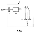
- a spectroscope for a second embodiment of the present invention is shown in Fig. 8 to provide a short time response and a small-sized device.
- a spectroscope 40 includes a deflection plate 41, which controls the deflection of incident light, a beam deflector 42, which is formed of a crystal having an electro-optic effect, a diffraction grating 43, which serves as spectroscopic means, a slit plate 44, which serves as wavelength selection means, and a photodetector 45.
- a diffraction grating is employed as spectroscopic means, instead of the prism used in the first embodiment.
- the diffraction grating 43 is a square with 20 mm sides, and 150 grooves/mm are formed in the surface.
- the length of an optical path, extending from the beam deflector 42 to the diffraction grating 43, is 20 mm. However, when a diffraction grating 43 having a smaller size is employed, the length of the optical path can be shortened.
- the wavelength range of incident light is 400 nm to 700 nm.
- the beam deflector 42, the diffraction grating 43, the slit plate 44 and the photodetector 45 are located so that upon application of a voltage of -85 V to the beam deflector 42, light is input to the diffraction grating 43 at an incidence angle of 43.5 degrees, and the diffracted light having a wavelength of 700 nm passes through the slit plate 44 and is detected by the photodetector 45. Subsequently, light output by the beam deflector 42 is dispersed, by the diffraction grating 43, in accordance with the wavelength.
- the wavelength of the light that is permitted to pass through the slit plate 44 can be selected from the incident light.
- the angle at which the incident light is input to the diffraction grating 43 is varied, between 43.5 degrees and 47.8 degrees.
- Light having a wavelength covering from 700 nm to 400 nm then passes through the slit plate 44, and is detected by the photodetector 45. At this time, only a period on the order of microseconds is required to sweep the wavelength range of from 700 nm to 400 nm.
- the slit width of the slit plate is 200 ⁇ m, and the wavelength resolution depends on a beam divergence angle, the number of grooves in the diffraction grating 43, the angle of incidence for the diffraction grating 43, and the distance between the diffraction grating 43 and the slit plate 44.
- the beam diameter of the beam deflector 42 is 400 ⁇ m
- 150 grooves/mm are provided for the diffraction grating 43
- the angle of incidence for the diffraction grating 43 is 43.5 degrees
- the distance from the diffraction grating 43 to the slit plate 44 is 120 mm.
- the wavelength resolution is about 4.5 nm near a wavelength of 400 nm, or about 9 nm near a wavelength of 700 nm.
- either the prism or the diffraction grating, which is spectroscopic means, is rotated to change the incidence angle for the incident light
- the beam deflector which is formed of a crystal having an electro-optic effect
- the spectroscope consumes only a small amount of power, and since a thermal control mechanism is not required, a smaller spectroscope can be provided.
- the arrangements in the first and second embodiments provide the above described effects and superior spectroscopes, they are very useful. These arrangements become even more useful since it is possible to obtain a high resolution without increasing the deflection angle of the beam deflector 12 or 42, or to reduce the voltage that is applied to the beam deflector 12 or 42 to acquire a predetermined resolution.
- a spectroscope that employs a prism, as spectroscopic means (a spectroscopic medium), with which a high resolution can be obtained without increasing the deflection angle for light output by a beam deflector, which includes an electro-optic crystal having an electro-optic effect, and for which, to acquire a predetermined resolution, a voltage applied to the beam deflector can be reduced.
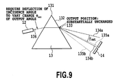
- Fig. 9 is a diagram for explaining the principle of spectroscopy for the the third embodiment.
- reference numeral 131 denotes the apex of a prism 13
- reference numeral 132 denotes the output plane of the prism 13, through which the light projected by the beam deflector 12 is output.
- Reference numeral 134a denotes light (also called output light 134a), which is part of the_light output by the prism 13 under a first voltage applied state of the beam deflector 12, that has the longest wavelength in a desired wavelength range for detection.
- reference numeral 134b denotes light (also called output light 134b), which is part of the light output by the prism 13 in the first voltage applied state of the beam deflector 12, that has the shortest wavelength in the desired wavelength range.
- Reference numeral 135a denotes light (also called output light 135a), which is part of the light output by the prism 13 when the beam deflector 12 is in a second voltage applied state differing from the first voltage applied state, that has the longest wavelength in a desired wavelength range for detection.
- reference numeral 135b denotes light (also called output light 135b), which is part of the light output by the prism 13 under the second voltage applied state of the beam deflector 12, that has the shortest wavelength in the desired wavelength range.
- the wavelength of light passing through the slit plate 14 be changed in accordance with the state under which the voltage is applied to the beam deflector 12.
- this condition is established in the following manner. Based on light having a wavelength that passes through the slit plate 14 and is detected by the photodetector 15, the individual voltage applied states of the beam deflector 12 are adjusted to control the deflection angle of light output by the beam deflector, and the angle at which light from the beam deflector 12 enters the prism 134 is changed.
- refraction at the output plane 132 for light having a long wavelength in a desired wavelength range to be detected should be greater than that for light having a short wavelength.
- the angle of incidence is controlled by the deflection of light that is output by the beam deflector 12, and the voltage applied state of the beam deflector 12 is controlled so that refraction at the output plane 132 for light detected that has a short wavelength is greater than that for light having a long wavelength.
- a voltage applied state is designated for deflecting the angle at which the incident light 136 enters the prism 13, so that a change ⁇ out varies for the output angle that is formed by the optical axes of light beams, output at the output plane 132, that have the longest wavelength and the shortest wavelength in a desired wavelength range to be detected.
- the voltage applied state of the beam deflector 12 indicates the level of a voltage (the strength of an electric field that is formed) that is applied to the KTN crystal 21 using the electrodes 22 and 23, and includes the state in which a voltage is not applied.
- the first voltage applied state is the state in which light having the shortest wavelength in a desired wavelength range for detection passes through the slit in the slit plate 14. Needless to say, an appropriate voltage applied state must be prepared for the detection of light having a wavelength lying between the longest and the shortest wavelengths in the desired wavelength range for detection.
- the deflection direction for light from the beam deflector 12 that enters the prism 13 is changed in accordance with the voltage applied state of the beam deflector 12.
- the input light is shown as light having a predetermined direction (input light 136), regardless of the application of a voltage to the beam deflector 12.
- the length of the example optical path from the beam deflector 12 to the prism 13 is 20 mm.
- the beam deflector 12 when the input light 136 has entered the prism 13 from the beam deflector 12, there is virtually no change in the input position on the incidence plane of the prism 13, whether the beam deflector 12 is in the first voltage applied state (corresponding to when light having the longest wavelength is detected in a desired wavelength range) or in the second voltage applied state (corresponding to when light having the longest wavelength is detected in the desired wavelength range). Therefore, in both the first voltage applied state and the second voltage applied state, light that enters and passes through the prism 13 is output at almost the same output position 133.
- a prism 13 having a high dispersion factor is required, and the deflection angle of the beam deflector 12 must be increased.
- a voltage applied to the beam deflector 12 must be increased.
- the deflection angle of the input light 136 which is projected from the beam deflector 12, must be increased, so that in the first voltage applied state, the light 134b having the shortest wavelength in the desired wavelength range for detection can pass through the slit in the slit plate 14, and in the second voltage applied state, the light 136 having the longest wavelength in the desired wavelength range can pass through the slit in the slit plate 14. Therefore, the level of a voltage applied to the beam deflector 12 must be increased to establish the second voltage applied state.
- performance at a high resolution indicates that light output by the spectroscopic means, such as a prism, is dispersed at a large angle in a wavelength range for detection. That is, an increase of the resolution can be provided by increasing an angle formed by the optical axis of the output light 134a and the optical axis of the output light 134b in Fig. 9 .
- the output angle of light should be changed by increasing the change in the deflection angle of the beam deflector 12, so that light across the entire wavelength range for detection can enter the slit of the slit plate 14. This is why, as described above, the voltage applied to the beam deflector 12 should be increased.
- the beamdeflector 12 and the prism 13 are located at a distance from each other, i.e., the optical path from the beam deflector 12 to the prism 13 is extended.
- the output position on the output plane 132 is shifted away from the output position, on the output plane 132, for light having a short wavelength that is to be detected.
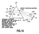
- Fig. 10 is a diagram for explaining the principle of spectroscopy according to this embodiment.
- reference numeral 140 denotes the output position of light on the output plane 132 while the beam deflector 12 is in the first voltage applied state.
- Reference numeral 141 denotes the output position of light on the output plane 132 while the beam deflector 12 is in the second voltage applied state.
- Reference numeral 142 denotes the incidence plane of the prism 13 for the arrangement wherein, in the structure in Fig. 9 (for a case wherein the optical path length between the beam deflector 12 and the prism 13 is 20 mm), the optical path between the beam deflector 12 and the prism 13 has an extended length (for a case wherein the length of the optical path from the beam deflector 12 to the prism 13 is 500 mm).
- Reference numeral 143 denotes the position on the incidence plane 142, at which light enters from the beam deflector 12 while in the first voltage applied state
- reference numeral 144 denotes the position on the incidence plane 142, at which light enters from the beam deflector while in the second voltage applied state.
- Reference numeral 145 denotes a virtual plane, which is the incidence plane of the prism 13 for light that enters from the beam deflector 12, assuming that the prism 13 is located at a distance of 20 mm from the beam deflector 12, as arranged in Fig. 10 (i.e., the arrangement in Fig. 9 is employed).
- Reference numeral 146 denotes the position, on the virtual incidence plane 145, at which light, from the beam deflector 12, enters in the first voltage applied state
- reference numeral 147 denotes the position on the virtual incidence plane 145 at which, based on the same assumption, light enters from the beam deflector 12 while in the second voltage applied state.
- the input position 146 for the first voltage applied state and the input position 147 for the second voltage applied state are not far from each other. Therefore, as shown in Fig. 9 , the output position on the prism 13 is not shifted, substantially, between the first voltage applied state and the second voltage applied state.
- the beam deflector 12 and the prism 13 are arranged at a distance as shown in Fig. 10 , the optical path from the beam deflector 12 to the prism 13 is extended, and as a result, the input position 143 for the first voltage applied state and the input position 144 for the second voltage applied state are located at a distance from each other. That is, the input position 144 on the incidence plane 142 in the second voltage applied state is shifted away from the input position 143 on the incidence plane 142 in the first voltage applied state.
- the optical path from the beam deflector 12 to the prism 13 is extended, for example, by increasing a distance between the beam deflector 12 and the prism 13, and the position at which light enters the prism 13 is shifted in accordance with the voltage applied state of the beam deflector 12. As a result, the position at which light is output from the prism 13 can be shifted.
- the output angle of the prism 13 is employed to control the input wavelength for the slit plate 14, while in this embodiment, both the output angle and the output position of the prism 13 are employed to control the input wavelength for the slit 14.
- this embodiment when the output position is shifted from the position 140 to the position 141, as shown in Fig. 10 , this encourages the change in wavelength to be detected, based on the change in the output angle. Therefore, when the same material is employed for a prism as a dispersion medium, the required deflection angle of the beam deflector 12 is smaller in the arrangement in Fig. 10 than in the arrangement in Fig. 9 , i.e., the level of voltage can be reduced.
- a high-dispersion prism should be employed to increase the change in the output angle, and the change in the deflection angle that determines the change in the output angle.
- shifting of the output position increases the change in the input wavelength for the slit plate 14, only smaller changes than those above are required for the output angle and the deflection angle. In other words, only a low voltage is required to obtain a high resolution.
- the beam deflector 12 which includes an electro-optic crystal, such as KTN, having an electro-optic effect
- the prism 13 which serves as spectroscopic means
- a shift in the output position at which light is output by the prism 13 (a distance between the output position 140 and the output position 141; an output shift distance) can be greater than a shift in the input position at which the light enters the prism 13 (the distance between the input position 143 and the input position 144; the input shift distance).
- the resolution can be improved without increasing the deflection angle of the beam deflector 12. Therefore, the improvement in resolution using a low drive voltage is enabled.
- the optical path between the beam deflector 12 and the prism 13 be designated to have an equal to or greater length than a length such that the output shift distance is increased.
- the output position is substantially unchanged, between the first voltage applied state and the second voltage applied state.
- angles are distributed at almost the same output position on the output plane of the prism 13, so that a long wavelength and a short wavelength in a desired wavelength range for detection. Therefore, to improve the resolution, a higher voltage must be applied to the beam deflector 12.
- the output position (the output position 140 in Fig. 10 ) for the detection of a short wavelength in a desired wavelength range) should differ from the output position (the output position 141 in Fig. 10 ) for the detection of a long wavelength in the desired wavelength range, i.e., the output position should be shifted.
- the output shift distance is considerably greater than the input shift distance, the output position can be greatly shifted. That is, when the optical path between the beam deflector 12 and the prism 13 is extended, the output position on the prism 13 is greatly shifted.
- the output position for the detection of a short wavelength in the desired wavelength range can be appropriately separated from the output position for the detection of a long wavelength in this wavelength range.
- This length refers to the predetermined optical path length previously described.
- the essence of this embodiment is that the beam deflector 12 and the prism 13 are arranged at a distance equivalent to a predetermined optical path length or longer.
- the present invention relates to a spectroscope, light having all the wavelengths in a targeted wavelength range (a desired wavelength range) be detected.
- a desired wavelength range a targeted wavelength range
- the output light 134b that is output at the output position 140 and has the shortest wavelength in the desired wavelength range be allowed to enter the slit in the slit plate 14
- the output light 135a that is output at the output position 141 and has the longest wavelength in the desired wavelength range be allowed to enter the slit in the slit plate 14.
- Fig. 11 is a diagram for explaining a condition, according to the embodiment, required to enable the detection of light having a wavelength in a desired wavelength range for detection.
- ⁇ 1 denotes an angle (also called an output angle ⁇ 1) formed, relative to the output plane 132 of the prism 13, by the optical axis of the output light 134b that is output on the output plane 132 in a case (first voltage applied state) wherein a voltage was applied to the beam deflector 12 for the detection of light having the shortest wavelength in a desired wavelength range.
- ⁇ 2 denotes an angle (also called an output angle ⁇ 2) formed, relative to the output plane 132 of the prism 13, by the optical axis of the output light 135a that is output on the output plane 132 in a case (a second voltage applied state) wherein a voltage was applied to the beam deflector 12 for the detection of light having the longest wavelength in the desired wavelength range.
- the output position on the output plane 132 of the prism 13 differs (is shifted) in accordance with the angle of deflection of light output by the beam deflector 12.
- the output position 141 of the output light 135a is shifted from the output position 140 of the output light 134b, and when the output angle ⁇ 1 is equal to the output angle ⁇ 2, i.e., when the output light 134b and the output light 135a are parallel to each other, the output light 135a, which is light having the longest wavelength in the desired wavelength range for detection, can not enter the slit in the slit plate 14.
- the light having the longest wavelength in the desired wavelength range can not be detected, and the detection of light in the desired wavelength range is not enabled.
- the output position is shifted between the first voltage applied state and the second voltage applied state to establish a condition ⁇ 1 ⁇ ⁇ 2, so that light having the longest wavelength and the shortest wavelength in a desired wavelength range can be detected.
- ⁇ 2 it is preferable that ⁇ 2 be as great as possible while ⁇ 1 ⁇ ⁇ 2 is satisfied.
- ⁇ 1 and ⁇ 2 are determined based on the length of the optical path, extended either between the beam deflector 12 and the prism 13 or in the prism, and a voltage applied to the KTN crystal 21 (the beam deflector 12). Therefore, in this embodiment, the first voltage applied state and the second voltage applied state are designated in accordance with the optical path length between the output position of the beam deflector 12 and the output position of the prism 13, so that a condition ⁇ 1 ⁇ ⁇ 2 is established.
- the beam deflector 12 Since it is important, for this embodiment, that the output position of the prism 13 be shifted based on the voltage applied state of the beam deflector 12, the beam deflector 12 is located at a distance from the prism 13, so that the input position for the prism 13 can be shifted based on the voltage applied state.
- the essential point is the extension of the optical path length between the beam deflector 12 and the prism 13, not the increase in the distance between the beam deflector 12 and the prism 13. That is, the essential point is not limited to a mode in which the distance between the beam deflector 12 and the prism 13 is physically extended.
- At least one mirror may be arranged between the beam deflector 12 and the prism 13, and light output by the beam deflector 12 may pass the mirror to enter the prism 13.
- An optical system employing a lens may also be employed. With this arrangement, a long optical path is obtained between the beam deflector 12 and the prism 13, although the beam deflector 12 and the prism 13 are physically located close to each other. Therefore, the size of the device can be reduced while extending the optical path from the beam deflector 12 to the prism 13.
- the output position of the prism 13 described above can be shifted. Therefore, when a large prism is employed instead of extending the optical path between the beam deflector 12 and the prism 13, the optical path length between the output position of the beam deflector 12 and the output position of the prism 13 can also be increased.
- the optical path from the beam deflector 12 to the prism 13 be extended and/or the size of the prism 13 be increased, in order to appropriately shift the output position of the prism 13 in the first voltage applied state and in the second voltage applied state.
- the photodetector 15 can not detect all of the light in the desired wavelength range simply by increasing the length of the optical path.
- one of the objectives of this embodiment is that the output position of the prism 13 be greatly changed for the detection of a long wavelength in a desired wavelength range and for the detection of a short wavelength in this wavelength range, and when the device functions as a spectroscope, it is important that both light having the longest wavelength and light having the shortest wavelength in the desired wavelength range should pass through the slit of the slit plate 14. That is, in this embodiment, it is important that light having the longest wavelength and light having the shortest wavelength in the desired wavelength range can be appropriately detected, regardless of whether, to improve the resolution, the optical path length between the beam deflector 12 and the prism 13 is increased, or a large prism is employed to extend the optical path for light that passes through the prism. Therefore, in this embodiment, based on the device structure that is provided, a voltage to be applied to the beam deflector 12 is designated to satisfy the condition ⁇ 1 ⁇ ⁇ 2.
- a large voltage is not required to be applied to the beam deflector 12 to provide a high resolution. That is, assuming that the same voltage is applied to the beam deflector 12 in this embodiment and to the beam deflector 12 in the first embodiment, a higher resolution can be obtained in this embodiment than in the first embodiment.
- a voltage applied to the beam deflector 12 in this embodiment can be lower than the voltage in the first embodiment.
- BK7 glass was employed as the prism 13 whose apex is 60°. Furthermore, a KTN crystal 21, 5 mm long and 0.5 mm thick, having a refractive index of 2.2 and S 11 of 1.0 x 10 14 m 2 /V 2 was employed for the beam deflector 12. The distance from the input position 143 to the apex 131 was 10 mm, and the distance from the output position to the slit plate 14 was 130 mm. A wavelength range of from 400 nm to 700 nm was to be detected for this example.
- the input positions (the input positions 143 and 144) for the prism 13 and the output positions (the output positions 140 and 141) for the prism 13 are determined based on a distance (an optical path length difference) L from the beam deflector 12 to the prism 13 and on the deflection angle of the beam deflector 12.
- ⁇ 3 is an angle at which the light output by the beam deflector 12 enters the prism at the input position 143 (an angle formed by the optical axis of light that enters the prism 13 and the incidence plane 142).
- F1 denotes a distance from the apex 131 to the output position 140
- ⁇ denotes the apex 131
- n denotes the refractive index of the prism 13
- F1 is represented by:
- F ⁇ 1 P ⁇ 1 ⁇ cos ⁇ + P ⁇ 1 ⁇ Tan ⁇ ⁇ - Sin - 1 1 / n ⁇ Sin ⁇ ⁇ Sin ⁇
- F2 is represented by:
- F ⁇ 2 P ⁇ 2 ⁇ cos ⁇ + P ⁇ 2 ⁇ Tan ⁇ ⁇ - Sin - 1 ⁇ 1 / n ⁇ Sin ⁇ ⁇ 3 - ⁇ ⁇ Sin ⁇
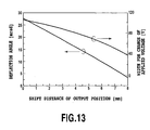
- Fig. 12 is a graph showing a relationship that was established, under the conditions represented in expressions (1) to (3), for a case wherein light was deflected by the beam deflector to detect the entire desired wavelength range, between a shift distance (F2 - F1) for the output positions for the prism 13 in the first voltage applied state and in the second voltage applied state, and the distance L from the beam deflector 12 to the prism 13.
- the deflection angle ⁇ is a deflection angle at which the beam deflector 12 is set in the second voltage applied state, i.e., a deflection angle required for performing spectroscopy to obtain light having the longest wavelength in the desired wavelength range. Therefore, when a low voltage (e.g., V ⁇ ) is set for the second voltage applied state to operate at a low drive voltage, simply a predetermined value need be designated for the shift distance between the output positions to obtain a satisfactorily high resolution. Then, an appropriate distance (optical path length difference) L can be obtained employing expressions (1) to (3).
- a shorter distance L is preferable while taking downsizing of the device into account; however, when the device is designed based on the above described relationship, only a little extension is required for the distance L, in the range 0 to 500 mm, to obtain a long output position shift distance.
- the distance L can be obtained to provide the output position shift distance required for a desired resolution. Therefore, the distance (optical path length difference) L between the beam deflector 12 and the prism 13 can be set to the optimal distance to obtain the desired resolution.
- the shift distance between the output positions is a large value, about 6 mm, which is substantially a fixed value. Therefore, from the viewpoint of this embodiment for increasing the output position shift distance to provide a high resolution at a low drive voltage, 500 mm or longer is preferable for the optical path between the beam deflector 12 and the prism 13.
- the shift distance for the output position is determined based on the length of the optical path between the beam deflector and the prism and the deflection angle of the beam deflector.
- the deflection angle of the beam deflector is shown in Fig. 13 , in correlation with the output position shift distance. This deflection angle indicates the deflection angle for the beam deflector required to detect a wavelength within a range of 400 nm to 700 nm.
- the distance between the beam deflector and the prism for the individual output position shift distance is as shown in Fig. 12 .
- the width for the change in an applied voltage is a difference between a voltage applied to detect a wavelength of 400 nm and a voltage applied to detect a wavelength of 700 nm.
- the deflection angle of the beam deflector is 28 mrad and the voltage applied is changed within the range of from +55 V to -55 V, and referring to Fig. 13 , 110 V is a difference between the voltage applied for detection of a wavelength of 400 nm and the voltage applied for detection of a wavelength of 700 nm.
- the distance (length of the optical path) between the beam deflector and the prism is 500 mm, 6 mm is obtained as the shift distance for the output position, and at this time, the deflection angle of 10 mrad is required for the beam deflector.
- a difference between the applied voltages is only 64 V, and a range only of from +32 V to -32 V is required to change the voltage applied. That is, only about 58% of a voltage need be applied, compared with when almost no shift appears in the output position (first basic arrangement). When the shift distance for the output position is increased, the effect produced by lowering the voltage applied becomes more noticeable.
- the effect in this embodiment is made more noticeable by dividing a voltage applied to the beam deflector 12 into two voltages: a DC voltage (bias voltage) used to determine the center of operating points, and an AC voltage used to control the wavelength of light that enters the slit of the slit plate 14.
- a DC voltage bias voltage
- AC voltage used to control the wavelength of light that enters the slit of the slit plate 14.
- the deflection angle of the beam deflector that includes an electro-optic crystal, such as KTN or KLTN is proportional to the square of the applied voltage, and when a change in the applied voltage is within the same range, the deflection angle is changed more greatly for a high voltage.
- a DC voltage (a bias voltage) for determining the center for the operating points is 240 V
- the range for the voltage change required to detect wavelengths of 400 nm to 700 nm is as shown in Table 3.
- a spectroscope which employs a diffraction grating as spectroscopic means (a spectroscopic medium) and for which a high resolution can be obtained without increasing the deflection angle of light output by a beam deflector that includes an electro-optic crystal having an electro-optic effect, and for which a voltage to be applied to the beam deflector can be lowered to acquire a predetermined resolution.
- the position at which light is output from a diffraction grating 43 be shifted, so that a high resolution can be obtained without increasing the deflection angle of light output by the beam deflector, and a voltage applied to the beam deflector can be lowered in order to obtain a predetermined resolution. For this reason, the length of the optical path between a beam deflector 42 and the diffraction grating 43 is increased. At this time, it is important that light having the longest wavelength and light having the shortest wavelength in a desired wavelength range can be detected to enable the detection of light having wavelengths in the entire desired wavelength range.
- the input position and the output position of the diffraction grating 43 are identical for light having a specific wavelength.
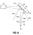
- Fig. 14 is a diagram for explaining a condition for this embodiment than enables the detection of light having a wavelength in a desired wavelength range.
- reference numeral 150 denotes a position at which light is output from an output surface 154 of the diffraction grating 43, for a case wherein the beam deflector 42 is in a third voltage applied state
- reference numeral 151 denotes a position at which light is output on the output surface 154, for a case wherein the beam deflector 42 is in a fourth voltage applied state.
- the third voltage applied state indicates the voltage applied state in which light having the longest wavelength in a desired wavelength range is allowed to pass through the slit in a slit plate 44.
- the fourth voltage applied state indicates the voltage applied state in which light having the shortest wavelength in the desired wavelength range is allowed to pass through the slit in the slit plate 44.
- Reference numeral 152a denotes light (also called output light 152a) that is included in light output by the diffraction grating 43 when it is in the third voltage applied state, and that has the shortest wavelength, in the desired wavelength range for detection.
- Reference numeral 152b denotes light (also called output light 152b) that is included in light output by the diffraction grating 43 when it is in the third voltage applied state, and that has the longest wavelength in the desired wavelength range for detection.
- Reference numeral 153a denotes light (also called output light 153a) that is included in light output by the diffraction grating 43 when it is in the fourth voltage applied state, and that has the shortest wavelength in the desired wavelength range for detection.
- Reference numeral 153b denotes light (also called output light 153b) that is included in light output by the diffraction grating 43 when it is in the fourth voltage applied state, and that has the longest wavelength in the desired wavelength range for detection.
- reference symbol ⁇ 1' denotes an angle (also called an output angle ⁇ 1') that is formed, relative to the output surface 154 of the diffraction grating 43, by the optical axis of the output light 152b diffracted on the output surface 154 in the state (the third voltage applied state) wherein a voltage is applied to the diffraction grating 43 for the detection of light having the longest wavelength in a desired wavelength range.
- Reference symbol ⁇ 2' denotes an angle (also called an output angle ⁇ 2') that is formed by, relative to the output surface 154 of the diffraction grating 43, the optical axis of the output light 153a diffracted on the output surface 154 in the state (the fourth voltage applied state) wherein a voltage is applied to the diffraction grating 43 for the detection of light having the shortest wavelength in the desired wavelength range.
- the beam deflector 42 is set to the third voltage applied state for the detection of light having the longest wavelength in the desired wavelength range for detection, and light output by the beam deflector 42 enters the output position 150. Then, the input light is dispersed at the output position 150, and light beams having individual frequencies that are diffracted from the output position 150 in consonance with their wavelengths. As a result, the output light 152 having the longest wavelength in the desired wavelength range enters the slit in the slit plate 44, and is detected by a photodetector 45.
- the beam deflector 42 When the beam deflector 42 is set to the fourth voltage applied state for the detection of light having the shortest wavelength in the desired wavelength range for detection, light output by the beam deflector 42 enters the diffraction grating 43 at the output position 151, which is shifted away from the output position 150. Therefore, in the fourth voltage applied state, dispersed light is output at the output position 151 that is different from that in the third voltage applied state. In this case, the output light 153a having the shortest wavelength in the desired wavelength range enters the slit of the slit plate 44, and is detected by the photodetector 45.
- the output light 152b in the third voltage applied state when the output light 152b in the third voltage applied state is parallel to the output light 153a in the fourth voltage applied state, the output light 153a can not enter the slit in the slit plate 44. Therefore, also in this embodiment, the length of the optical path between the output position of the beam deflector 42 and the output position of the diffraction grating 43 is employed to set the third voltage applied state and the fourth voltage applied state, so that a condition ⁇ 1' ⁇ 2' is established. At this time, it is preferable that ⁇ 2' be as great as possible while ⁇ 1' ⁇ ⁇ 2' is satisfied.
- the state in which a voltage is applied to the beam deflector is changed from the first voltage state to the second voltage state, or from the third voltage applied state to the fourth voltage applied state.
- changing the states is not limited to this.
- the state in which a voltage is applied to the beam deflector may be changed from the second voltage applied state to the first voltage applied state, or from the fourth voltage applied state to the third voltage applied state.
- the objective of this embodiment is simultaneous performance of high-resolution measurement and wideband measurement in one operation, in addition to reducing the time response and downsizing a device.
- chromatic dispersion at a wider angle is required using a dispersion medium, such as a prism.
- a deflection angle required for the beam deflector becomes greater.
- the refractive index dispersion of the dispersion medium must be lowered to conduct the wideband measurement, and in this case, the resolution would be degraded.
- a beam deflector that includes an electro-optic crystal, such as KTN
- KTN electro-optic crystal
- One beam of the separated light is employed for spectroscopy of the entire wavelength range to be measured, i.e., is employed for wideband measurement, and the other beam is employed for spectroscopy for one part of the wavelength range at a high resolution, i.e., is employed for high-resolution measurement.
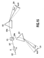
- Fig. 15 is a diagram illustrating a spectroscope according to this embodiment that can perform both high-resolution measurement and wideband measurement in one operation.
- a polarizing beam splitter 151 is located at the rear of a beam deflector 12 that includes a KTN crystal 21, and serves as means for outputting incident light in two different directions.
- p-polarization represents polarization in a direction that is perpendicular to the optical axis, and matches the direction of the electric field generated between electrodes arranged in the electro-optic crystal.
- p-polarization is in a direction perpendicular to the optical axis, and along the plane of the paper.
- s-polarization represents polarization in a direction that is perpendicular to the optical axis, and is orthogonal to the direction of the electric field generated between the electrodes of the electro-optic crystal.
- the s-polarization is in a direction perpendicular to the plane of the paper.
- the beam deflector 12 outputs the p-polarization component and the s-polarization component upon application of a voltage, for simplification of the drawing in Fig. 15 , the p-polarization component and the s-polarization component are collectively indicated as the light 157.
- the splitter 151 When the light 157 output by the beam deflector 12 enters the polarizing beam splitter 151, the splitter 151 separates the light 157 into the p-polarization component and the s-polarization component, and outputs these components in different directions. That is, the polarizing beam splitter 151 allows the p-polarization component of the input light 157 to pass through, and outputs this component as p-polarization light 158a. Further, the polarizing beam splitter 151 reflects the s-polarization component of the input light 157, and outputs this component as s-polarization light 158b.
- a prism 152 having a low refractive-index dispersion property (a small change in a refractive index according to a wavelength) is located on the side of the polarizing beam splitter 151 that outputs the light 158a.
- a prism 153 with a refractive-index dispersion property higher than that for the prism 152 (a large change in a refractive index according to a wavelength) is located on the side of the polarizing beam splitter 151 that outputs the light 158b.
- slit plates 154 and 155 are arranged as wavelength selection means respectively at the rear stages of the prisms 152 and 153.
- the incident light 156 that has an arbitrary polarization component, other than the p-polarization component and s-polarization component, enters the beam deflector 12.
- the p-polarization component and the s-polarization component are output by the beam deflector 12 at a predetermined deflection angle.
- the polarizing beam splitter 151 separates the input light 157 for the individual polarization components and outputs the light components in two different directions.
- the p-polarization component passes the polarization beam splitter 151, and enters the prism 152 as the light 158a, while the s-polarization component is reflected by the polarizing beam splitter 151, and enters the prism 153 as the light 158b.
- the light 158a is dispersed by the prism 152, and the entire wavelength range to be detected (the desired wavelength band) is measured by a photodetector (not shown) that is located at the rear of the slit plate 154.
- the detected wavelength range is 400 nm to 700 nm.
- the voltage application state required for the beam deflector 12, under which light having the longest wavelength in the desired wavelength range is permitted to pass through the slit plate 154 is defined as a fifth voltage applied state.
- the voltage application state required for the beam deflector 12, under which light having the shortest wavelength in the desired wavelength range is permitted to pass through the slit plate 155 is defined as a sixth voltage applied state.
- the entire desired wavelength range can be measured by changing the fifth voltage applied state to the sixth voltage applied state, as needed.
- a desired wavelength range for detection may be employed to designate the positions of the beam deflector 12, the polarizing beam splitter 151, the prism 152 and the slit plate 154, the material of the prism 152, the fifth and the sixth voltage applied states, etc.
- the other light 158b is dispersed by the prism 153, and only one part of the wavelength range for detection (the desired wavelength range) is measured, at a high resolution, using a photodetector (not shown) that is located at the rear of the slit plate 155.
- a wavelength range to be detected at a high resolution is 600 nm to 650 nm.
- the refractive index dispersion of the prism 153 is higher than the refractive index dispersion of the prism 152, which is used for detection of the entire desired wavelength range. Therefore, the prism 153 refracts light more than the prism 152.
- the wavelength range for example, of 500 nm to 750 nm is focused on, an angle formed by the optical axes of light having a wavelength of 500 nm and light having a wavelength of 750 nm, which are output by the prism 153 under a specific voltage applied state, is greater than an angle formed by the optical axes of light having a wavelength of 500 nm and light having a wavelength of 750 nm that are output by the prism 152.
- the width for a change in the wavelength is smaller for light that is output by the prism 153 and passes through the slit plate 155, than for light that is output by the prism 152 and passes through the slit plate 154.
- the prism 153 provides a higher resolution measurement than the prism 152. That is, in this embodiment, on the prism 153 side, detection of light having a wavelength of 600 nm is enabled in the fifth voltage applied state, and detection of light having a wavelength of 650 nm is enabled in the sixth voltage applied state.
- a desired wavelength range to be detected at a high resolution may be employed to designate the positions of the beam deflector 12, the polarizing beam splitter 151, the prism 153 and the slit plate 155, the material of the prism 153, the fifth voltage applied state and the sixth voltage applied state, etc.
- a measurement performed for the entire wavelength range to be detected and a measurement performed for one part of this wavelength range can be performed in only one operation, using the same device. That is, when the fifth voltage applied state is changed to the sixth voltage applied state, the entire wavelength range to be detected is measured on the prism 152 side, and one part of this wavelength range is measured on the prism 153 side.
- a wavelength range to be detected at a high resolution should be variable.
- a movable portion be provided for the slit plate 155 and that the slit plate 155 be moved as needed, so that a wavelength range to be detected at a high resolution can be varied.
- a wavelength range (e.g., 600 nm to 650 nm) can be fixed for high-resolution detection.
- a wavelength range for high-resolution detection can be varied by moving the slit plate 155.
- the slit plate 155 need simply be located along a rail, for example, and be manually moved, as desired.
- a power controller such as an actuator, may be provided to automatically move the slit plate 155.
- the wavelength range of light that enters the slit plate 155 becomes a desired wavelength range to be detected at a high resolution. Therefore, the wavelength range of light is changed in accordance with the position of the slit plate 155.
- the movable slit plate 155 for this embodiment is employed, a variable wavelength range is obtained for light that enters the slit plate 155.
- the position of the slit plate 155 is determined based on a desired wavelength range to be detected at a high resolution, so that when the fifth voltage applied state is changed to the sixth voltage applied state, light in the desired wavelength range enters the slit plate 155. In this manner, a variable wavelength range can be detected at a high resolution.
- the prism 152 which has a relatively low refractive index dispersion property
- the prism 153 which has a relatively high refractive index dispersion property
- the light 156 used for measurement is deflected by the beam deflector 12 and is separated into two beams, and these beams enter the prism 152, which has the low refractive index dispersion property
- the prism 153 which has the high refractive index dispersion property, to perform spectroscopy. Therefore, the entire desired wavelength range can be measured on the prism 152 side, while at the same time, a high-resolution measurement can be performed on the prism 153 side.
- the light deflected by the beam deflector 12 is separated into light used for measurement of the entire desired wavelength range to be detected and light used for high-resolution measurement, only the voltage control for the beam deflector 12 is required to perform both the measurement of the entire wavelength range and the high-resolution measurement.
- either the p-polarization component or the s-polarization may be employed for measurement of the entire wavelength range to be detected and for high-resolution measurement.
- the p-polarization component when employed, the high-resolution measurement is enabled for the same wavelength range, or wide-range measurement is enabled for the same resolution.
- the polarizing beam splitter 151 it is important that light deflected by the beam deflector 12 be separated into two beams to enter the prism 152 and the prism 153, and the use of the polarizing beam splitter 151 is not essential. Further, arbitrary means, such as a half-silvered mirror, may be employed for this embodiment, instead of the polarizing beam splitter 151, so long as the arbitrary means can separate and output incident light in two different directions.
- the p-polarization component or the s-polarization component enter the prisms 152 and 153 to perform appropriate measurement.
- the secondary electro-optic constants s 11 and s 12 of the KTN crystal 21 are provided with signs that are inverted from each other, the s-polarization component and the p-polarization component are deflected in opposite directions. Therefore, when the p-polarization component is employed for the individual prisms to perform measurement, the s-polarization component also enters the prisms and could adversely affect the measurement when the polarity of a voltage, applied to the beam deflector 12, is changed. This is why using either the p-polarization component or the s-polarization component is appropriate when a half-silvered mirror is employed.
- a polarizer can be located in front of the beam deflector 12 to allow either the p-polarization component or the s-polarization component to enter the beam deflector 12.
- the essential point of this embodiment is that the incident light 156 to be measured is separated, and that one of the separated lights enters the prism 152 to measure the entire desired wavelength range, while the other beam of the separated light enters the prism 153 to perform the high-resolution measurement.
- the incident light 156 may be separated into two beams to the front of the beam deflector 12, as shown in Fig. 16 .
- reference numeral 161 denotes a ⁇ /2 wave plate and reference numeral 162 denotes a mirror.
- the ⁇ /2 wave plate be employed to change the polarization direction of the s-polarization component that is separated by the polarizing beam splitter 151. That is, when the ⁇ /2 wave plate 161 is arranged to the rear of the polarizing beam splitter 151, from which the s-polarization component is output, the p-polarization component can enter both of the prisms 152 and 153.
- ⁇ /2 wave plate 161 is not necessarily provided.
- the mirror 162 is arranged to the rear of the ⁇ /2 wave plate 161, and is employed to change the direction of light that is output by the ⁇ /2 wave plate 161.
- the beam deflector 12 may also be located along the optical paths of the light beams that are obtained by the polarizing beam splitter 151.
- the objective of this embodiment is the provision of high sensitivity for a spectroscope, in addition to securing a short time response and a small-sized device.
- a beam deflector that includes an electro-optic crystal, such as KTN, and that the size of an opening in the input surface of the beam deflector be enlarged. Enlarging of the opening is especially important for spectroscopy of incoherent light that is difficult to concentrate, or to collimate at a small spot.
- a beam deflector includes an electro-optic crystal, such as KTN, having a secondary electro-optic effect, and deflects a light beam by generating the inclination of a refractive index between electrodes.
- an opening is enlarged, when a distance between the electrodes (thickness of the crystal) is a times, a voltage of a ⁇ a times is required to obtain the same deflection angle for the beam deflector.
- an electro-optic crystal such as KTN, employed in this embodiment, has a thickness (a distance between the electrodes) that is maintained at a value required to provide a specific deflection angle, and a width that is greater than the thickness, so that the opening can be enlarged in the input surface of the beam deflector without increasing the voltage that is required to obtain the specific deflection angle. Further, light having an elliptic shape in cross section is allowed to enter the beam deflector.
- the “thickness (of the electro-optic crystal)” represents the length of an electro-optic crystal from one face to the other on which the electrodes are arranged.
- the “width (of the electro-optic crystal)” represents the width of the electro-optic crystal in a direction across the thickness of the electro-optic crystal, or perpendicular to the direction in which light propagates in the electro-optic crystal.
- Fig. 18 is a perspective view of a beam deflector according to this embodiment.
- the width of a KTN crystal 21 is greater than the thickness. Therefore, the size of an opening in an input surface 181 of the beam deflector 12 can be increased, without changing the distance between electrodes 22 and 23. As a result, the raising of a required voltage can be prevented, even when the opening is enlarged.
- incident light 182 having an elliptic shape in cross section enters the input surface 181.
- the quantity of light input can be increased by a value equivalent to the extension of the long axis of the elliptic shape of the incident light 182 in cross section. Therefore, high sensitivity can be obtained for a spectroscope, without increasing the level of a required voltage.
- the incident light 182 which has an elliptic shape in cross section
- Means that facilitates the entry, to the input surface 182, of light having an elliptic shape in cross section is not limited to a cylindrical lens or a slit, and arbitrary means can be employed so long as the means can output the incident light as light having an elliptic shape in cross section.
- the opening can be enlarged by increasing the thickness of the KTN crystal 21; however, since the distance between the electrodes 22 and 23 is extended, as previously described, a higher voltage is required to obtain the same deflection angle.
- the direction of width that does not affect a required voltage is controlled, instead of controlling the thickness that affects a voltage, so that the opening size is enlarged without causing a rise in the voltage that is required. That is, the width of the KTN crystal 21 is set so greater than the thickness, while the voltage required for providing a specific deflection angle is maintained, i.e., while a thickness correlated with the required voltage is maintained. As a result, the size of the opening can be increased.
- the incident light 182 can appropriately enter the beam deflector 12, even when the light is incoherent light.
- the radius of the circle that is the cross section of the incident light becomes a limiting factor, from the viewpoint of the quantity of light input. Therefore, regardless of whether the opening is enlarged by increasing the width of the KTN crystal 21, the thickness of the KTN crystal 21 will not be increased, and an increase of the quantity of light input is not anticipated.
- the incident light 182 since the incident light 182 has an elliptic shape in cross section, the long axis of the elliptic shape of the incident light 182 can be increased by a length equivalent to an extension of the width of the KTN crystal 21. Accordingly, the quantity of light input to the beam deflector 12 can be increased, and the sensitivity can be improved.
- the size of the opening in the input surface of the beam deflector be enlarged, so that even incoherent light can be appropriately coupled with the beam deflector.
- the thickness of the electro-optic crystal is multiplied a times to extend the opening, a voltage required for the same deflection angle could be raised a ⁇ a times, and a voltage rise would have occurred. Therefore, in this embodiment, the width of an electro-optic crystal employed is greater than the thickness, so that the opening size can be extended while an increase in a required voltage can be prevented.
- the beam deflector when the beam deflector is provided by setting the width of the electro-optic crystal so greater than the thickness, thereby obtaining a large opening and preventing a rise in the level of a required voltage, incident light having an elliptic shape, in cross section, can enter the input surface of the beam deflector, so that the long axis of the elliptic shape is parallel to the width of the electro-optic crystal.
- the quantity of light input to the beam deflector can be increased and a high-sensitivity spectroscope can be provided.
- the objective of this embodiment is the provision of a simple, high-resolution spectroscope, in addition to securing a short time response and the downsizing of a device.
- a beam deflector and spectroscopic means such as a prism, like those that have been employed in the first to the sixth embodiments, can be provided using a single device.
- Fig. 19 is a diagram illustrating a spectroscope according to this embodiment.
- a spectroscope 190 includes a KTN crystal 191.
- An electrode 192 is formed on a first face of the KTN crystal 191, and an electrode 193 is formed on a second face, opposite the first face.
- Reference numeral 194 denotes the input end of the spectroscope 190
- reference numeral 195 denotes the output end of the spectroscope 190.
- the output end 195 of the spectroscope 190 (the KTN crystal 191) is wedge shaped, at an angle inward of the plane where a light beam is deflected by the application of a voltage, thereby providing a wedge shaped output end 196. That is, the wedge shaped output end 196 is formed at the output end 195, so that its thickness is gradually reduced and a slope is formed from the second face, where the electrode 193 is formed, toward the first face, where the electrode 192 is formed.
- the wedge shaped forming process can be performed by producing the beam deflector 12, shown in Fig. 5 , and cutting or grinding the output end.
- the light output from the wedge shaped output end 196 can be distributed in accordance with the state in which a voltage is applied to the electrodes 192 and 193.
- the output end 195 has an wedge shaped output end that forms an angle in a direction perpendicular to the plane where a light beam is deflected (referring to Fig. 19 , the wedged output end that is gradually thinned from the front on paper (or the rear on paper) to the rear on paper (or the front on paper)), the beam deflection direction does not match the dispersing direction using the slope of the wedge, and therefore, the device does not function as a spectroscope.
- the direction in which the thickness of the KTN crystal 191 is changed matches the direction in which the electric field is applied, the dispersing direction and the beam deflection direction are identical at the wedge shaped output end 196.
- the device can appropriately function as a spectroscope.
- an electro-optic crystal such as KTN
- KTN electro-optic crystal
- a refractive index is high for a short wavelength
- the output angle of each wavelength is changed when the light has reached the interface obliquely.
- the wedge shaped output end 196 is employed for this embodiment, light can be dispersed and output at the output end 196 for the individual wavelengths. Further, since the wedge shaped output end 196 is formed so that the direction in which the thickness is gradually reduced matches the direction of the electric field formed between the electrodes 192 and 193, the direction in which dispersed light is spread (the dispersing direction) can match the beam deflection direction, and the function of a spectroscope can be provided.
- a dispersing medium such as a prism or a diffraction grating, may be arranged to the rear of the spectroscope 190.
- the end to be wedge shaped is not limited to the output end, and may be the input end ( Fig. 20A ), or both the input end and the output end ( Figs. 20B or 20C ).
- Figs. 21 and 22 show relationships between an angle at which light that propagated in the KTN crystal 191 has reached the output end 195, and a dispersion angle that is a change in the angle at which light is externally output from the crystal.
- a difference in the output angle between the wavelengths 700 nm and 400 nm is described as a dispersion angle.
- the deflection angle inside the KTN crystal 191 is -50 mrad to 50 mrad, regardless of the wavelength.
- the example in Fig. 21 is a relationship established for a case wherein the output end 195 is not wedge shaped.
- the deflection angle inside the KTN crystal 195 is increased so the light obliquely reaches the output end 195, and the dispersion angle outside the crystal is also increased, but only to about 1 mrad.
- the example in Fig. 22 is provided for a case wherein the output end 195 is wedge shaped, so that an angle of 20 degrees (349 mrad) is formed relative to the wedge shaped output end 196 of the KTN crystal 191, when light is not deflected inside the KTN crystal 191, and shows a relationship established between the angle at which light reaches the wedge shaped output end 196 of the KTN crystal 191 and the dispersion angle.
- a refractive index difference is 0.1
- the maximum dispersion angle is 8 mrad
- the refractive index difference is 0.2
- the obtained dispersion angle is 19 mrad, at the maximum.
- the angle relative to the output end of the KTN crystal 191 is large, the dispersion angle is increased and remarkable effects can be obtained using the wedge shaped end.
- such a device can function as a spectroscope, and a spectroscope having a simple structure can be provided.
Landscapes
- Physics & Mathematics (AREA)
- Spectroscopy & Molecular Physics (AREA)
- General Physics & Mathematics (AREA)
- Spectrometry And Color Measurement (AREA)
- Optical Modulation, Optical Deflection, Nonlinear Optics, Optical Demodulation, Optical Logic Elements (AREA)
- Analysing Materials By The Use Of Radiation (AREA)
Claims (6)
- Spectroscope, comprenant :un déviateur de faisceau (12) qui comporte un cristal KTN (21) ayant une composition KTa1-xNbxO3 ou une composition K1-yLiyTa1-xNbxO3 (0<x<1, 0<y<1), ayant un effet électro-optique, et des électrodes appariées (22, 23) utilisées pour appliquer un champ électrique à l'intérieur du cristal KTN (21) ;un prisme (13) pour disperser une lumière délivrée en sortie par le déviateur de faisceau (12) ; etun moyen de sélection de longueur d'onde (14) pour sélectionner une lumière ayant une longueur d'onde arbitraire à partir de la lumière dispersée et délivrée en sortie par le prisme (13) ;dans lequel le déviateur de faisceau (12) délivre en sortie la lumière à différents angles de déviation dans un premier état de tension appliquée, dans lequel la tension est appliquée aux électrodes appariées (22, 23) pour la détection de la lumière ayant la longueur d'onde la plus courte dans une plage de longueur d'onde souhaitée pour la détection, et dans un deuxième état de tension appliquée dans lequel la tension est appliquée aux électrodes appariées (22, 23) pour la détection de la lumière ayant la longueur d'onde la plus longue dans la plage de longueur d'onde souhaitée pour la détection ;dans lequel le déviateur de faisceau (12) et le prisme (13) sont disposés à une distance équivalente à une longueur de trajet optique prédéterminée de sorte que la position d'entrée (143, 144 ; 150, 151), au niveau du prisme (13), d'un faisceau lumineux provenant du déviateur de faisceau (12) vers le prisme (13) soit différente au premier état de tension appliquée et au deuxième état de tension appliquée, et où le déviateur de faisceau (12) et le prisme (13) sont disposés de sorte qu'un angle d'entrée au prisme (13), qui est formé par un axe optique du faisceau lumineux entrant dans le prisme (13) et un plan d'incidence (142) formé par la surface du prisme (13), soit le plus petit dans le premier état de tension appliquée et l'angle d'entrée au prisme (13) est le plus grand dans le deuxième état de tension appliquée ;dans lequel le moyen de sélection de longueur d'onde (14) est disposé au niveau de la position où l'axe optique de la lumière de longueur d'onde la plus courte délivrée en sortie à partir du prisme (13) au premier état de tension appliquée et l'axe optique de la lumière de longueur d'onde la plus longue délivrée en sortie à partir du prisme (13) au deuxième état de tension appliquée sont croisés.
- Spectroscope selon la revendication 1, dans lequel une largeur pour le déviateur de faisceau (12) est supérieure à une épaisseur pour le déviateur de faisceau (12).
- Spectroscope selon la revendication 2, comprenant en outre :un moyen configuré pour projeter, au déviateur de faisceau (12), une lumière ayant une forme elliptique, en coupe transversale, où la lumière ayant la forme elliptique, en coupe transversale, pénètre le déviateur de faisceau (12), de sorte qu'une direction le long de l'axe long de la forme elliptique corresponde à la direction de la largeur du déviateur de faisceau (12).
- Spectroscope selon la revendication 1, comprenant en outre un polariseur (11) configuré pour projeter, sur le déviateur de faisceau (12), une lumière constituée seulement d'un composant le long d'un axe de polarisation, qui est parallèle au champ électrique.
- Spectroscope selon la revendication 1, dans lequel lorsque F1 désigne une distance depuis le sommet (131) du prisme (13) à une position de sortie (140) de la lumière, β désigne le sommet (131), n désigne l'indice de réfraction du prisme (13), P1 désigne une distance entre le sommet (131) et la position d'entrée (143) de la lumière, et θ3 désigne l'angle d'entrée au prisme (13) avec lequel la lumière délivrée en sortie par le déviateur de faisceau (12) pénètre le prisme (13) au niveau de la position d'entrée (143), F1 est représentée par :

où, lorsque F2 désigne une distance depuis le sommet (131) à la position de sortie (141), Φ désigne un angle de déviation nécessaire pour déplacer une position depuis la position d'entrée (143) à la position d'entrée (144), et P2 désigne une distance depuis le sommet (131) à la position d'entrée (144), F2 est représentée par :
- Spectroscope selon la revendication 1, dans lequel le moyen de sélection de longueur d'onde (14) est une plaque fendue.
Priority Applications (2)
| Application Number | Priority Date | Filing Date | Title |
|---|---|---|---|
| EP11183117.8A EP2402726B1 (fr) | 2007-07-31 | 2008-07-30 | Spectroscope |
| EP11183115.2A EP2402725B1 (fr) | 2007-07-31 | 2008-07-30 | Spectroscope |
Applications Claiming Priority (3)
| Application Number | Priority Date | Filing Date | Title |
|---|---|---|---|
| JP2007199741 | 2007-07-31 | ||
| JP2008165624 | 2008-06-25 | ||
| PCT/JP2008/063629 WO2009017142A1 (fr) | 2007-07-31 | 2008-07-30 | Spectroscope |
Related Child Applications (4)
| Application Number | Title | Priority Date | Filing Date |
|---|---|---|---|
| EP11183115.2A Division EP2402725B1 (fr) | 2007-07-31 | 2008-07-30 | Spectroscope |
| EP11183117.8A Division EP2402726B1 (fr) | 2007-07-31 | 2008-07-30 | Spectroscope |
| EP11183117.8 Division-Into | 2011-09-28 | ||
| EP11183115.2 Division-Into | 2011-09-28 |
Publications (3)
| Publication Number | Publication Date |
|---|---|
| EP2175251A1 EP2175251A1 (fr) | 2010-04-14 |
| EP2175251A4 EP2175251A4 (fr) | 2010-09-22 |
| EP2175251B1 true EP2175251B1 (fr) | 2013-05-15 |
Family
ID=40304372
Family Applications (3)
| Application Number | Title | Priority Date | Filing Date |
|---|---|---|---|
| EP08791860.3A Active EP2175251B1 (fr) | 2007-07-31 | 2008-07-30 | Spectroscope |
| EP11183117.8A Active EP2402726B1 (fr) | 2007-07-31 | 2008-07-30 | Spectroscope |
| EP11183115.2A Active EP2402725B1 (fr) | 2007-07-31 | 2008-07-30 | Spectroscope |
Family Applications After (2)
| Application Number | Title | Priority Date | Filing Date |
|---|---|---|---|
| EP11183117.8A Active EP2402726B1 (fr) | 2007-07-31 | 2008-07-30 | Spectroscope |
| EP11183115.2A Active EP2402725B1 (fr) | 2007-07-31 | 2008-07-30 | Spectroscope |
Country Status (5)
| Country | Link |
|---|---|
| US (1) | US8274653B2 (fr) |
| EP (3) | EP2175251B1 (fr) |
| JP (3) | JPWO2009017142A1 (fr) |
| CN (1) | CN101688808B (fr) |
| WO (1) | WO2009017142A1 (fr) |
Families Citing this family (14)
| Publication number | Priority date | Publication date | Assignee | Title |
|---|---|---|---|---|
| US8284809B2 (en) * | 2009-03-23 | 2012-10-09 | Lawrence Livermore National Security, Llc | Laser bandwidth interlock capable of single pulse detection and rejection |
| CN101887201B (zh) * | 2010-06-29 | 2013-06-05 | 中国科学院深圳先进技术研究院 | 波长选择装置 |
| JP2012163395A (ja) * | 2011-02-04 | 2012-08-30 | Ricoh Co Ltd | 分光装置 |
| CN102692734B (zh) * | 2012-06-07 | 2014-07-16 | 山东省科学院新材料研究所 | 一种基于ktn晶体二次电光效应的激光偏转调制方法 |
| CN103048118A (zh) * | 2012-08-24 | 2013-04-17 | 王艳文 | 一种快速定位三棱镜最小偏向角的方法 |
| JP2014134499A (ja) * | 2013-01-11 | 2014-07-24 | Nippon Telegr & Teleph Corp <Ntt> | 光干渉断層装置 |
| CN103969719A (zh) * | 2014-04-11 | 2014-08-06 | 京东方科技集团股份有限公司 | 一种三棱镜板和显示装置 |
| CN105572073B (zh) * | 2015-12-31 | 2018-05-18 | 哈尔滨工业大学 | 一种外加电场条件下测量液体折射率的方法 |
| CN105466888B (zh) * | 2015-12-31 | 2018-05-18 | 哈尔滨工业大学 | 一种外加电场条件下测量液体折射率的装置 |
| KR102539143B1 (ko) | 2016-09-21 | 2023-06-01 | 삼성전자주식회사 | 분광기 및 분광기 모듈 |
| CN111007057A (zh) * | 2019-12-23 | 2020-04-14 | 哈尔滨工业大学(威海) | 通用型重金属单元素检测仪及其应用方法 |
| EP3964815A4 (fr) * | 2020-07-09 | 2022-08-03 | Shenzhen Hypernano Optics Technology Co., Ltd | Système et procédé de test de la vitesse de réponse spectrale d'un filtre accordable |
| US20230266164A1 (en) * | 2020-07-15 | 2023-08-24 | Nippon Telegraph And Telephone Corporation | Spectroscopic device, spectrometry device, and spectroscopic method |
| CN113551779A (zh) * | 2021-08-11 | 2021-10-26 | 电子科技大学 | 一种用于航空发动机涡轮叶片测温的棱镜六通道系统 |
Family Cites Families (13)
| Publication number | Priority date | Publication date | Assignee | Title |
|---|---|---|---|---|
| US3462212A (en) * | 1965-10-18 | 1969-08-19 | Bell Telephone Labor Inc | Polychromatic beam deflection |
| US3667038A (en) * | 1970-06-17 | 1972-05-30 | Hewlett Packard Co | Acousto-optic rf spectrum analysis method and apparatus |
| JPH08159867A (ja) * | 1994-12-05 | 1996-06-21 | Hamamatsu Photonics Kk | 光波形測定装置 |
| JPH09145477A (ja) * | 1995-11-20 | 1997-06-06 | Tokyo Instr:Kk | 分光器 |
| JP3349353B2 (ja) * | 1996-07-30 | 2002-11-25 | 三菱重工業株式会社 | レーザを用いた固体粒子成分解析装置 |
| JP2000205954A (ja) * | 1999-01-08 | 2000-07-28 | Naba:Kk | 分光装置 |
| US6759235B2 (en) * | 2000-04-06 | 2004-07-06 | Quantum Dot Corporation | Two-dimensional spectral imaging system |
| CN2454767Y (zh) * | 2000-12-19 | 2001-10-17 | 中国科学院安徽光学精密机械研究所 | 机械扫描式高速光谱采集装置 |
| JP2003207394A (ja) * | 2002-01-10 | 2003-07-25 | Yokogawa Electric Corp | 分光測定装置 |
| JP2004286582A (ja) * | 2003-03-20 | 2004-10-14 | Nippon Telegr & Teleph Corp <Ntt> | 電界検出光学装置およびトランシーバ |
| JP4646506B2 (ja) * | 2003-09-11 | 2011-03-09 | オリンパス株式会社 | レーザ走査型顕微鏡 |
| JP4640577B2 (ja) * | 2004-11-12 | 2011-03-02 | 横河電機株式会社 | 光スペクトラムアナライザ |
| JP2008040089A (ja) * | 2006-08-04 | 2008-02-21 | Seiko Epson Corp | 電気光学素子及び走査型光学装置 |
-
2008
- 2008-07-30 WO PCT/JP2008/063629 patent/WO2009017142A1/fr active Application Filing
- 2008-07-30 EP EP08791860.3A patent/EP2175251B1/fr active Active
- 2008-07-30 CN CN2008800235616A patent/CN101688808B/zh active Active
- 2008-07-30 US US12/667,753 patent/US8274653B2/en active Active
- 2008-07-30 EP EP11183117.8A patent/EP2402726B1/fr active Active
- 2008-07-30 JP JP2009525425A patent/JPWO2009017142A1/ja active Pending
- 2008-07-30 EP EP11183115.2A patent/EP2402725B1/fr active Active
-
2012
- 2012-08-14 JP JP2012179850A patent/JP2012215595A/ja active Pending
-
2013
- 2013-07-19 JP JP2013150643A patent/JP5649246B2/ja active Active
Also Published As
| Publication number | Publication date |
|---|---|
| EP2402725B1 (fr) | 2017-09-27 |
| EP2175251A1 (fr) | 2010-04-14 |
| EP2175251A4 (fr) | 2010-09-22 |
| EP2402726A1 (fr) | 2012-01-04 |
| JP2013213838A (ja) | 2013-10-17 |
| JPWO2009017142A1 (ja) | 2010-10-21 |
| CN101688808B (zh) | 2012-01-25 |
| JP5649246B2 (ja) | 2015-01-07 |
| JP2012215595A (ja) | 2012-11-08 |
| US20110058166A1 (en) | 2011-03-10 |
| EP2402725A1 (fr) | 2012-01-04 |
| WO2009017142A1 (fr) | 2009-02-05 |
| US8274653B2 (en) | 2012-09-25 |
| CN101688808A (zh) | 2010-03-31 |
| EP2402726B1 (fr) | 2016-09-07 |
Similar Documents
| Publication | Publication Date | Title |
|---|---|---|
| EP2175251B1 (fr) | Spectroscope | |
| US9645291B1 (en) | Voltage-tunable optical filters for instrumentation applications | |
| US4905169A (en) | Method and apparatus for simultaneously measuring a plurality of spectral wavelengths present in electromagnetic radiation | |
| EP0250070B1 (fr) | Méthode optique d'analyse et appareil à accès rapide programmable à longueur d'onde accidentelle | |
| US7601977B2 (en) | Phase-matched terahertz emitter | |
| JP4514430B2 (ja) | 液晶系偏光分析装置 | |
| US7616308B2 (en) | Optical measurement apparatus and method | |
| JPH0473748B2 (fr) | ||
| EP0180449A2 (fr) | Filtre de dispersion accusto-optique | |
| US20070103778A1 (en) | Device for dispersing light pulses of which the spectral amplitude is programmable | |
| TW201518696A (zh) | 光譜系統以及基於梳的光譜法的方法 | |
| US11239626B2 (en) | Multi-pass etalon filter | |
| US4256405A (en) | Scanning spectrometer | |
| JP4640577B2 (ja) | 光スペクトラムアナライザ | |
| US9128059B2 (en) | Coherent anti-stokes raman spectroscopy | |
| US6204926B1 (en) | Methods and system for optically correlating ultrashort optical waveforms | |
| JPH0357942A (ja) | 干渉計形検出装置 | |
| Kawata | Instrumentation for near-infrared spectroscopy | |
| EP0851268A2 (fr) | Filtre acouto-optique accordable | |
| JP2023500015A (ja) | ラマンスペクトルを測定するための装置及びその方法 | |
| JP5584126B2 (ja) | 微小素子の特性決定方法及び装置 | |
| JP6549448B2 (ja) | 自己相関測定装置 | |
| JP7435784B2 (ja) | 分光装置、分光測定装置および分光方法 | |
| JP2008535018A (ja) | 繰返し光パルス信号の極短光パルスを検出し、それらの光パルスのパルス幅を決定する方法および装置 | |
| JP2020085545A (ja) | 光空間計測装置 |
Legal Events
| Date | Code | Title | Description |
|---|---|---|---|
| PUAI | Public reference made under article 153(3) epc to a published international application that has entered the european phase |
Free format text: ORIGINAL CODE: 0009012 |
|
| 17P | Request for examination filed |
Effective date: 20100112 |
|
| AK | Designated contracting states |
Kind code of ref document: A1 Designated state(s): AT BE BG CH CY CZ DE DK EE ES FI FR GB GR HR HU IE IS IT LI LT LU LV MC MT NL NO PL PT RO SE SI SK TR |
|
| AX | Request for extension of the european patent |
Extension state: AL BA MK RS |
|
| A4 | Supplementary search report drawn up and despatched |
Effective date: 20100820 |
|
| DAX | Request for extension of the european patent (deleted) | ||
| 17Q | First examination report despatched |
Effective date: 20110519 |
|
| GRAP | Despatch of communication of intention to grant a patent |
Free format text: ORIGINAL CODE: EPIDOSNIGR1 |
|
| GRAS | Grant fee paid |
Free format text: ORIGINAL CODE: EPIDOSNIGR3 |
|
| GRAA | (expected) grant |
Free format text: ORIGINAL CODE: 0009210 |
|
| AK | Designated contracting states |
Kind code of ref document: B1 Designated state(s): AT BE BG CH CY CZ DE DK EE ES FI FR GB GR HR HU IE IS IT LI LT LU LV MC MT NL NO PL PT RO SE SI SK TR |
|
| REG | Reference to a national code |
Ref country code: GB Ref legal event code: FG4D Ref country code: CH Ref legal event code: EP |
|
| REG | Reference to a national code |
Ref country code: AT Ref legal event code: REF Ref document number: 612384 Country of ref document: AT Kind code of ref document: T Effective date: 20130615 |
|
| REG | Reference to a national code |
Ref country code: IE Ref legal event code: FG4D |
|
| REG | Reference to a national code |
Ref country code: DE Ref legal event code: R096 Ref document number: 602008024616 Country of ref document: DE Effective date: 20130711 |
|
| REG | Reference to a national code |
Ref country code: AT Ref legal event code: MK05 Ref document number: 612384 Country of ref document: AT Kind code of ref document: T Effective date: 20130515 |
|
| REG | Reference to a national code |
Ref country code: LT Ref legal event code: MG4D |
|
| REG | Reference to a national code |
Ref country code: NL Ref legal event code: VDEP Effective date: 20130515 |
|
| PG25 | Lapsed in a contracting state [announced via postgrant information from national office to epo] |
Ref country code: NO Free format text: LAPSE BECAUSE OF FAILURE TO SUBMIT A TRANSLATION OF THE DESCRIPTION OR TO PAY THE FEE WITHIN THE PRESCRIBED TIME-LIMIT Effective date: 20130815 Ref country code: ES Free format text: LAPSE BECAUSE OF FAILURE TO SUBMIT A TRANSLATION OF THE DESCRIPTION OR TO PAY THE FEE WITHIN THE PRESCRIBED TIME-LIMIT Effective date: 20130826 Ref country code: LT Free format text: LAPSE BECAUSE OF FAILURE TO SUBMIT A TRANSLATION OF THE DESCRIPTION OR TO PAY THE FEE WITHIN THE PRESCRIBED TIME-LIMIT Effective date: 20130515 Ref country code: AT Free format text: LAPSE BECAUSE OF FAILURE TO SUBMIT A TRANSLATION OF THE DESCRIPTION OR TO PAY THE FEE WITHIN THE PRESCRIBED TIME-LIMIT Effective date: 20130515 Ref country code: GR Free format text: LAPSE BECAUSE OF FAILURE TO SUBMIT A TRANSLATION OF THE DESCRIPTION OR TO PAY THE FEE WITHIN THE PRESCRIBED TIME-LIMIT Effective date: 20130816 Ref country code: SE Free format text: LAPSE BECAUSE OF FAILURE TO SUBMIT A TRANSLATION OF THE DESCRIPTION OR TO PAY THE FEE WITHIN THE PRESCRIBED TIME-LIMIT Effective date: 20130515 Ref country code: PT Free format text: LAPSE BECAUSE OF FAILURE TO SUBMIT A TRANSLATION OF THE DESCRIPTION OR TO PAY THE FEE WITHIN THE PRESCRIBED TIME-LIMIT Effective date: 20130916 Ref country code: SI Free format text: LAPSE BECAUSE OF FAILURE TO SUBMIT A TRANSLATION OF THE DESCRIPTION OR TO PAY THE FEE WITHIN THE PRESCRIBED TIME-LIMIT Effective date: 20130515 Ref country code: IS Free format text: LAPSE BECAUSE OF FAILURE TO SUBMIT A TRANSLATION OF THE DESCRIPTION OR TO PAY THE FEE WITHIN THE PRESCRIBED TIME-LIMIT Effective date: 20130915 Ref country code: FI Free format text: LAPSE BECAUSE OF FAILURE TO SUBMIT A TRANSLATION OF THE DESCRIPTION OR TO PAY THE FEE WITHIN THE PRESCRIBED TIME-LIMIT Effective date: 20130515 |
|
| PG25 | Lapsed in a contracting state [announced via postgrant information from national office to epo] |
Ref country code: PL Free format text: LAPSE BECAUSE OF FAILURE TO SUBMIT A TRANSLATION OF THE DESCRIPTION OR TO PAY THE FEE WITHIN THE PRESCRIBED TIME-LIMIT Effective date: 20130515 Ref country code: BG Free format text: LAPSE BECAUSE OF FAILURE TO SUBMIT A TRANSLATION OF THE DESCRIPTION OR TO PAY THE FEE WITHIN THE PRESCRIBED TIME-LIMIT Effective date: 20130815 Ref country code: HR Free format text: LAPSE BECAUSE OF FAILURE TO SUBMIT A TRANSLATION OF THE DESCRIPTION OR TO PAY THE FEE WITHIN THE PRESCRIBED TIME-LIMIT Effective date: 20130515 |
|
| PG25 | Lapsed in a contracting state [announced via postgrant information from national office to epo] |
Ref country code: LV Free format text: LAPSE BECAUSE OF FAILURE TO SUBMIT A TRANSLATION OF THE DESCRIPTION OR TO PAY THE FEE WITHIN THE PRESCRIBED TIME-LIMIT Effective date: 20130515 |
|
| PG25 | Lapsed in a contracting state [announced via postgrant information from national office to epo] |
Ref country code: EE Free format text: LAPSE BECAUSE OF FAILURE TO SUBMIT A TRANSLATION OF THE DESCRIPTION OR TO PAY THE FEE WITHIN THE PRESCRIBED TIME-LIMIT Effective date: 20130515 Ref country code: BE Free format text: LAPSE BECAUSE OF FAILURE TO SUBMIT A TRANSLATION OF THE DESCRIPTION OR TO PAY THE FEE WITHIN THE PRESCRIBED TIME-LIMIT Effective date: 20130515 Ref country code: CZ Free format text: LAPSE BECAUSE OF FAILURE TO SUBMIT A TRANSLATION OF THE DESCRIPTION OR TO PAY THE FEE WITHIN THE PRESCRIBED TIME-LIMIT Effective date: 20130515 Ref country code: SK Free format text: LAPSE BECAUSE OF FAILURE TO SUBMIT A TRANSLATION OF THE DESCRIPTION OR TO PAY THE FEE WITHIN THE PRESCRIBED TIME-LIMIT Effective date: 20130515 Ref country code: DK Free format text: LAPSE BECAUSE OF FAILURE TO SUBMIT A TRANSLATION OF THE DESCRIPTION OR TO PAY THE FEE WITHIN THE PRESCRIBED TIME-LIMIT Effective date: 20130515 |
|
| PG25 | Lapsed in a contracting state [announced via postgrant information from national office to epo] |
Ref country code: RO Free format text: LAPSE BECAUSE OF FAILURE TO SUBMIT A TRANSLATION OF THE DESCRIPTION OR TO PAY THE FEE WITHIN THE PRESCRIBED TIME-LIMIT Effective date: 20130515 Ref country code: IT Free format text: LAPSE BECAUSE OF FAILURE TO SUBMIT A TRANSLATION OF THE DESCRIPTION OR TO PAY THE FEE WITHIN THE PRESCRIBED TIME-LIMIT Effective date: 20130515 Ref country code: NL Free format text: LAPSE BECAUSE OF FAILURE TO SUBMIT A TRANSLATION OF THE DESCRIPTION OR TO PAY THE FEE WITHIN THE PRESCRIBED TIME-LIMIT Effective date: 20130515 Ref country code: MC Free format text: LAPSE BECAUSE OF FAILURE TO SUBMIT A TRANSLATION OF THE DESCRIPTION OR TO PAY THE FEE WITHIN THE PRESCRIBED TIME-LIMIT Effective date: 20130515 |
|
| REG | Reference to a national code |
Ref country code: CH Ref legal event code: PL |
|
| PLBE | No opposition filed within time limit |
Free format text: ORIGINAL CODE: 0009261 |
|
| STAA | Information on the status of an ep patent application or granted ep patent |
Free format text: STATUS: NO OPPOSITION FILED WITHIN TIME LIMIT |
|
| 26N | No opposition filed |
Effective date: 20140218 |
|
| REG | Reference to a national code |
Ref country code: IE Ref legal event code: MM4A |
|
| PG25 | Lapsed in a contracting state [announced via postgrant information from national office to epo] |
Ref country code: CH Free format text: LAPSE BECAUSE OF NON-PAYMENT OF DUE FEES Effective date: 20130731 Ref country code: LI Free format text: LAPSE BECAUSE OF NON-PAYMENT OF DUE FEES Effective date: 20130731 |
|
| REG | Reference to a national code |
Ref country code: DE Ref legal event code: R097 Ref document number: 602008024616 Country of ref document: DE Effective date: 20140218 |
|
| PG25 | Lapsed in a contracting state [announced via postgrant information from national office to epo] |
Ref country code: IE Free format text: LAPSE BECAUSE OF NON-PAYMENT OF DUE FEES Effective date: 20130730 |
|
| PG25 | Lapsed in a contracting state [announced via postgrant information from national office to epo] |
Ref country code: CY Free format text: LAPSE BECAUSE OF FAILURE TO SUBMIT A TRANSLATION OF THE DESCRIPTION OR TO PAY THE FEE WITHIN THE PRESCRIBED TIME-LIMIT Effective date: 20130515 Ref country code: MT Free format text: LAPSE BECAUSE OF FAILURE TO SUBMIT A TRANSLATION OF THE DESCRIPTION OR TO PAY THE FEE WITHIN THE PRESCRIBED TIME-LIMIT Effective date: 20130515 Ref country code: TR Free format text: LAPSE BECAUSE OF FAILURE TO SUBMIT A TRANSLATION OF THE DESCRIPTION OR TO PAY THE FEE WITHIN THE PRESCRIBED TIME-LIMIT Effective date: 20130515 |
|
| PG25 | Lapsed in a contracting state [announced via postgrant information from national office to epo] |
Ref country code: HU Free format text: LAPSE BECAUSE OF FAILURE TO SUBMIT A TRANSLATION OF THE DESCRIPTION OR TO PAY THE FEE WITHIN THE PRESCRIBED TIME-LIMIT; INVALID AB INITIO Effective date: 20080730 Ref country code: LU Free format text: LAPSE BECAUSE OF NON-PAYMENT OF DUE FEES Effective date: 20130730 |
|
| REG | Reference to a national code |
Ref country code: FR Ref legal event code: PLFP Year of fee payment: 9 |
|
| REG | Reference to a national code |
Ref country code: FR Ref legal event code: PLFP Year of fee payment: 10 |
|
| REG | Reference to a national code |
Ref country code: FR Ref legal event code: PLFP Year of fee payment: 11 |
|
| PGFP | Annual fee paid to national office [announced via postgrant information from national office to epo] |
Ref country code: GB Payment date: 20230720 Year of fee payment: 16 |
|
| PGFP | Annual fee paid to national office [announced via postgrant information from national office to epo] |
Ref country code: FR Payment date: 20230725 Year of fee payment: 16 Ref country code: DE Payment date: 20230719 Year of fee payment: 16 |