EP2162762B1 - Virtueller pet-detektor und quasi-gepixeltes ableseschema für pet - Google Patents
Virtueller pet-detektor und quasi-gepixeltes ableseschema für pet Download PDFInfo
- Publication number
- EP2162762B1 EP2162762B1 EP08738026.7A EP08738026A EP2162762B1 EP 2162762 B1 EP2162762 B1 EP 2162762B1 EP 08738026 A EP08738026 A EP 08738026A EP 2162762 B1 EP2162762 B1 EP 2162762B1
- Authority
- EP
- European Patent Office
- Prior art keywords
- photodetectors
- time stamp
- virtual pixel
- photodetector
- gamma ray
- Prior art date
- Legal status (The legal status is an assumption and is not a legal conclusion. Google has not performed a legal analysis and makes no representation as to the accuracy of the status listed.)
- Active
Links
- 239000013078 crystal Substances 0.000 claims description 72
- 238000000034 method Methods 0.000 claims description 25
- 230000005251 gamma ray Effects 0.000 claims description 21
- 238000003491 array Methods 0.000 claims description 8
- 238000002059 diagnostic imaging Methods 0.000 claims description 5
- 230000008569 process Effects 0.000 claims description 2
- 230000004044 response Effects 0.000 claims description 2
- 238000010200 validation analysis Methods 0.000 description 12
- 238000002600 positron emission tomography Methods 0.000 description 11
- 230000008901 benefit Effects 0.000 description 7
- 238000001514 detection method Methods 0.000 description 6
- 230000008878 coupling Effects 0.000 description 5
- 238000010168 coupling process Methods 0.000 description 5
- 238000005859 coupling reaction Methods 0.000 description 5
- 238000013461 design Methods 0.000 description 5
- 238000004519 manufacturing process Methods 0.000 description 5
- 238000002603 single-photon emission computed tomography Methods 0.000 description 5
- XUIMIQQOPSSXEZ-UHFFFAOYSA-N Silicon Chemical compound [Si] XUIMIQQOPSSXEZ-UHFFFAOYSA-N 0.000 description 4
- 238000003384 imaging method Methods 0.000 description 4
- 229910052710 silicon Inorganic materials 0.000 description 4
- 239000010703 silicon Substances 0.000 description 4
- 239000000872 buffer Substances 0.000 description 3
- 238000013507 mapping Methods 0.000 description 3
- 229940121896 radiopharmaceutical Drugs 0.000 description 3
- 239000012217 radiopharmaceutical Substances 0.000 description 3
- 230000002799 radiopharmaceutical effect Effects 0.000 description 3
- 238000012879 PET imaging Methods 0.000 description 2
- 230000006399 behavior Effects 0.000 description 2
- 210000004556 brain Anatomy 0.000 description 2
- 230000000694 effects Effects 0.000 description 2
- 230000010354 integration Effects 0.000 description 2
- 230000005855 radiation Effects 0.000 description 2
- 238000012546 transfer Methods 0.000 description 2
- WQZGKKKJIJFFOK-GASJEMHNSA-N Glucose Natural products OC[C@H]1OC(O)[C@H](O)[C@@H](O)[C@@H]1O WQZGKKKJIJFFOK-GASJEMHNSA-N 0.000 description 1
- 206010028980 Neoplasm Diseases 0.000 description 1
- 201000011510 cancer Diseases 0.000 description 1
- 230000015556 catabolic process Effects 0.000 description 1
- 238000006243 chemical reaction Methods 0.000 description 1
- 230000001010 compromised effect Effects 0.000 description 1
- 230000007812 deficiency Effects 0.000 description 1
- 230000001934 delay Effects 0.000 description 1
- 230000001747 exhibiting effect Effects 0.000 description 1
- 239000008103 glucose Substances 0.000 description 1
- 239000003292 glue Substances 0.000 description 1
- 230000003993 interaction Effects 0.000 description 1
- 238000005259 measurement Methods 0.000 description 1
- 238000012636 positron electron tomography Methods 0.000 description 1
- 238000012545 processing Methods 0.000 description 1
- 230000002285 radioactive effect Effects 0.000 description 1
- 230000009467 reduction Effects 0.000 description 1
- 230000035945 sensitivity Effects 0.000 description 1
- 239000007787 solid Substances 0.000 description 1
- 239000012536 storage buffer Substances 0.000 description 1
- 230000033772 system development Effects 0.000 description 1
- 238000012360 testing method Methods 0.000 description 1
- 230000007704 transition Effects 0.000 description 1
- 238000012795 verification Methods 0.000 description 1
- 238000004876 x-ray fluorescence Methods 0.000 description 1
Images
Classifications
-
- G—PHYSICS
- G01—MEASURING; TESTING
- G01T—MEASUREMENT OF NUCLEAR OR X-RADIATION
- G01T1/00—Measuring X-radiation, gamma radiation, corpuscular radiation, or cosmic radiation
- G01T1/16—Measuring radiation intensity
- G01T1/20—Measuring radiation intensity with scintillation detectors
- G01T1/202—Measuring radiation intensity with scintillation detectors the detector being a crystal
-
- G—PHYSICS
- G01—MEASURING; TESTING
- G01T—MEASUREMENT OF NUCLEAR OR X-RADIATION
- G01T1/00—Measuring X-radiation, gamma radiation, corpuscular radiation, or cosmic radiation
- G01T1/16—Measuring radiation intensity
- G01T1/161—Applications in the field of nuclear medicine, e.g. in vivo counting
- G01T1/164—Scintigraphy
- G01T1/1641—Static instruments for imaging the distribution of radioactivity in one or two dimensions using one or several scintillating elements; Radio-isotope cameras
- G01T1/1644—Static instruments for imaging the distribution of radioactivity in one or two dimensions using one or several scintillating elements; Radio-isotope cameras using an array of optically separate scintillation elements permitting direct location of scintillations
-
- A—HUMAN NECESSITIES
- A61—MEDICAL OR VETERINARY SCIENCE; HYGIENE
- A61B—DIAGNOSIS; SURGERY; IDENTIFICATION
- A61B6/00—Apparatus for radiation diagnosis, e.g. combined with radiation therapy equipment
- A61B6/02—Devices for diagnosis sequentially in different planes; Stereoscopic radiation diagnosis
- A61B6/03—Computerised tomographs
- A61B6/037—Emission tomography
-
- G—PHYSICS
- G01—MEASURING; TESTING
- G01T—MEASUREMENT OF NUCLEAR OR X-RADIATION
- G01T1/00—Measuring X-radiation, gamma radiation, corpuscular radiation, or cosmic radiation
- G01T1/16—Measuring radiation intensity
- G01T1/161—Applications in the field of nuclear medicine, e.g. in vivo counting
- G01T1/164—Scintigraphy
- G01T1/1641—Static instruments for imaging the distribution of radioactivity in one or two dimensions using one or several scintillating elements; Radio-isotope cameras
- G01T1/1642—Static instruments for imaging the distribution of radioactivity in one or two dimensions using one or several scintillating elements; Radio-isotope cameras using a scintillation crystal and position sensing photodetector arrays, e.g. ANGER cameras
-
- G—PHYSICS
- G01—MEASURING; TESTING
- G01T—MEASUREMENT OF NUCLEAR OR X-RADIATION
- G01T1/00—Measuring X-radiation, gamma radiation, corpuscular radiation, or cosmic radiation
- G01T1/16—Measuring radiation intensity
- G01T1/20—Measuring radiation intensity with scintillation detectors
- G01T1/2018—Scintillation-photodiode combinations
- G01T1/20184—Detector read-out circuitry, e.g. for clearing of traps, compensating for traps or compensating for direct hits
-
- G—PHYSICS
- G01—MEASURING; TESTING
- G01T—MEASUREMENT OF NUCLEAR OR X-RADIATION
- G01T1/00—Measuring X-radiation, gamma radiation, corpuscular radiation, or cosmic radiation
- G01T1/29—Measurement performed on radiation beams, e.g. position or section of the beam; Measurement of spatial distribution of radiation
- G01T1/2914—Measurement of spatial distribution of radiation
- G01T1/2985—In depth localisation, e.g. using positron emitters; Tomographic imaging (longitudinal and transverse section imaging; apparatus for radiation diagnosis sequentially in different planes, steroscopic radiation diagnosis)
Definitions
- PET positron emission tomography
- SPECT single photon emission computed tomography
- Scintillator pixel size in PET is a primary factor determining the spatial resolution of the resulting image.
- the scanner geometry and pixel size are optimized to maximize the scanner performance and competitiveness.
- typical pixel size used in a full-body scanner is 4x4 mm 2
- a pixel size of 2x2 mm 2 to 1x1 mm 2 may be used to increase the resolution.
- a 1:1 coupling between scintillator pixels and photo-detectors is often used to optimize performance, and translates into a need for a custom-designed light detector for each specific application. This, however, implies significant changes to the light detection chain as well. In conventional systems using photomultiplier tubes and Anger logic, this further means that the light guide design and the size of the photomultiplier tubes must be adapted, thus leading to higher system development and manufacturing costs.
- each scintillator element improves spatial resolution, and the plurality of detectors can determine where in the scintillator the scintillation event occurs.
- timing resolution for determining time-of-flight measurements can be compromised, since each of the multiple detectors only sees a fraction of the light and may receive it with different delays.
- coupling each scintillator with a corresponding detector optimizes the timing resolution, but reduces spatial resolution.
- the single detector that receives all of the light from the crystal can provide an accurate time stamp, but resolution is limited to the size of the scintillator.
- the scintillator crystals are coupled to the light detectors either on 1:1 basis (pixelated readout) or through a light guide using Anger logic for crystal identification.
- pixelated readout is the vast number of channels and, as the crystal size gets smaller, the cost of the photodetectors.
- Anger logic-based systems map many crystals onto few photodetectors, leading to smaller number of channels at the cost of increased pile-up and dead time and thus reduced count rate capability.
- WO 2006/111883 A2 discloses a radiation detector that includes an array of detector pixels each including an array of detector cells. Each detector cell includes a photodiode biased in a breakdown region and digital circuitry coupled with the photodiode and configured to output a first digital value in a quiescent state and a second digital value responsive to photon detection by the photodiode. Digital triggering circuitry is configured to output a trigger signal indicative of a start of an integration time period responsive to a selected number of one or more of the detector cells transitioning from the first digital value to the second digital value.; Readout digital circuitry accumulates a count of a number of transitions of detector cells of the array of detector cells from the first digital state to the second digital state over the integration time period.
- a virtual pixel for a diagnostic imaging system is defined in claim 1.
- a method of calculating a time stamp for a virtual pixel is defined in claim 4.
- One advantage is that detector array design cost is reduced.
- Another advantage resides in a universal detector array chip for multiple sizes of scanners.
- Another advantage resides in improved compatibility between detector arrays or scanners utilizing crystals of different sizes.
- FIGURE 1 illustrates a virtual pixel that is employed on a detector chip that is configured to be optically coupled with any of a variety of scintillator arrays (not shown).
- a "virtual" pixel can be a configurable combination of photodetectors and scintillator crystals, designed to act or appear as a given standard type of detector, such as a 4x4 array of 1x1mm 2 photodetectors, or some other size array of a given size of photodetectors.
- the universal chip reduces manufacturing costs by enabling the same chip to be used on a variety of PET scanners.
- CMOS-based photodetector The redesign, manufacturing and testing of a new CMOS-based photodetector is a costly endeavor.
- This problem can be surmounted by combining several small pixels into larger virtual pixels, which can be performed either in hardware, or in software.
- four solid state detectors can be arranged in a square and can be operated as four independent detectors, grouped together to operate as a single detector, etc.
- the virtual pixel facilitates introducing virtualization to PET detectors based on a digital silicon photomultiplier, which integrates the light sensing element and the readout circuits onto the chip.
- the virtual pixel illustrated in Figure 1 shows a software-based virtualization scheme
- subsequent figures show additional circuits that facilitate connecting several smaller photodetectors 12 into larger virtual pixels, which are matched to the application without sacrificing detector performance.
- a one-size-fits-all detector is designed, thus saving costs on design and manufacturing and leading to improved readout performance compared to a monolithic pixel of the same size.
- the virtual pixel comprises a scintillator crystal 10 of a given size and multiple smaller photodetector pixels 12.
- a virtualizer 14 e.g. a processor
- a final "hit" which describes a perceived gamma ray registration event at a portion of the virtual pixel crystal.
- hardware that improves timing resolution and reduces data rate may be employed in conjunction with the virtual pixel.
- the following example is presented to illustrate a scenario in which the virtual pixels are useful. For instance, it may be desirable to implement a photodetector with a smallest practical pixel size, such as 1x1 mm 2 in the case of an animal scanner, and then glue larger crystals to 2x2 or 4x4 photodetectors, if the detector is to be used in a brain or a human scanner.
- a photodetector with a smallest practical pixel size, such as 1x1 mm 2 in the case of an animal scanner, and then glue larger crystals to 2x2 or 4x4 photodetectors, if the detector is to be used in a brain or a human scanner.
- either 4 or 16 photodetector pixels can detect the photons emitted from the crystal and an external logic, implemented in a separate field programmable gate array (FPGA) or the like, can combine the pixels to get the energy and the time of the gamma hit.
- FPGA field programmable gate array
- the trigger lines of the photodetectors can be combined together in a symmetrical way, as described below with regard to Figure 2 .
- software may be employed to permit a user to select (e.g., via a pull-down menu or some other interface) virtual pixel size based on an application for which the virtual pixel is to be employed in a detector array.
- Software may also be employed to select active trigger lines in a hard virtual pixel, which facilitates manipulating behavior of the virtual pixel.
- FIGURE 2 shows a hardware-based virtual pixel that is employed on a universal chip in a manner similar to the software-based virtual pixel described above.
- the virtual pixel includes trigger lines 22 that connect smaller photodetectors 12 comprised by the virtual pixel.
- time-to-digital converters (TDC) 26 can be employed to measure the time of the first photon arriving at any of the combined pixels.
- TDC time-to-digital converters
- a combination of the validation signal is employed to validate the resulting hit, as described in U.S. Patent Application No. 11/467,670 , entitled “Digital Silicon Photomultiplier,” filed on August 28, 2006. The validation signal is used to determine if the event is a real hit or if the acquisition has been started by a dark count.
- a validation signal is useful because the first cell that fires stops the TDC and starts the acquisition. Therefore, in the case of a dark count, the validation prevents the pixel from executing a full acquisition and then discarding the data right afterwards. Doing so would increase the dead time of the pixel, as any hit during that time would lead to an incorrect time stamp and also likely to an incorrect energy.
- a trigger network is hierarchically subdivided into vertical column lines that trigger a horizontal trigger line, which is then connected to the TDC.
- the validation of a hit means that more than one column trigger line indicates a hit for the hit to be validated. For instance, according to an example, if four columns exhibit activity within approximately 5 ns, then the event can be considered a real hit. Otherwise, the pixel can be quickly reset to get prepare for the next hit.
- the probability of detecting 4 dark counts in a respective line within 5 ns is sufficiently low to make the foregoing validation scheme highly efficient.
- at least one of the photodetectors validates the hit.
- the photodetectors 12 included in the virtual pixel contribute directly to the time stamp of the hit, as their trigger lines are connected through a balanced network connected to an additional TDC component 26 .
- the TDC component includes an accumulator as well, which sums partial photon counts from the respective photodetectors comprised by the virtual pixel.
- the photon statistics remain substantially unchanged.
- a 2x2mm 2 virtual pixel is shown in Figure 2 , four of the virtual pixels can be used to implement a 4x4mm 2 pixel, if desired, and so on.
- a selector/multiplexer 28 selects which data to forward to one or more output buffers (not shown).
- software determines which trigger lines to activate in the hard virtual pixel in order to manipulate pixel behavior.
- the time stamp and energy of the final hit are computed by an algorithm, which can also be implemented in an external FPGA for performance reasons, if desired.
- the algorithm uses the time stamps and energies from all pixels included in the virtual pixel, and computes the time stamp and the energy of the hit as if all pixels were connected together. While computing the total energy is straightforward, computing the time stamp can be more complicated.
- the time stamp can be computed in a way similar to that which is used in Anger-logic, as an energy-weighted sum of the partial time-stamps. That is, as illustrated in Figure 2A , each of the four illustrated detectors responds to the scintillation with a respective pulse A, B, C, and D, whose beginning is indicative of time and whose area is indicative of energy.
- this method involves several multiply-add operations and a fixed-point division to be implemented in hardware.
- Another method uses the time stamp of the hit with the highest energy (e.g., C, in the example of Figure 2A ), assuming this time stamp to be most accurate because of the photon statistics.
- the earliest timestamp (e.g., A, in Figure 2A ) can be used independently of the energy of the partial hit - this method mimics the hard-wiring of the trigger lines of the virtual pixels.
- error e.g., quantum noise, TDC shifts, and numerical errors
- soft virtualization is relatively cheap and does not need any additional hardware, which can lead to a potentially higher manufacturing yield because of a lower number of gates.
- FIGURE 3 is an illustration of a hardware-based virtual pixel that facilitates using Anger logic to determine a time stamp for a gamma ray hit on the virtual pixel.
- a photodetector chip can be optimized for a scanner with 2x2mm 2 crystals, as shown in the figure.
- the same chip can be used in a full-body scanner, where 2x2 pixels are combined to realize a 4x4mm 2 virtual pixel with timing resolution optimized for time of flight (TOF).
- TOF time of flight
- the same detector could also be connected to a light guide and 1x1mm 2 crystals, for instance in an animal scanner.
- a mapping scheme can also be used without a light guide.
- the circuitry implementing the Anger logic can be placed on the chip itself, thus making the type of readout transparent to the rest of the system.
- the orientation of the photodetector pixels 12 comprised by the virtual pixel can be optimized to minimize any "dead area" due to the electronics, as shown in Figure 3 . Additionally, space between pixels 12 can be utilized for processing circuitry and the like.
- the trigger network 22 forms a symmetrical balanced tree of buffers.
- hit validation logic (not shown) is connected in a similar way to facilitate separating triggers due to dark counts from the real hits. At least one of the validation signals from each pixel can indicate a valid hit for the acquisition to continue.
- the validation logic in the real pixels can be superseded by the validation logic of the virtual pixel in order to accomplish this.
- the acquisition sequence can be controlled by a virtual pixel state machine.
- the readout time of the virtual pixel is substantially identical to the readout time of the small pixels making up the virtual pixel, compared to a monolithic large pixel where the readout time increases with pixel size. This is the result of the parallel readout of the smaller pixels, which can be done faster than in a large pixel having more lines to read.
- a combination of both hard and soft virtual pixels is possible.
- a combination of separate hard and soft virtual pixels can be employed in a single virtual pixel array.
- a single virtual pixel can employ any or all of the features of a soft virtual pixel, such as described with regard to Figure 1 , as well as any or all of the features of a hard virtual pixel, such as described with regard to Figures 2 and 3 .
- a virtual pixel array whether employing soft or hard virtual pixels, can employ virtual pixels of different sizes, in order to localize a desired pixel size on a given region of interest or the like.
- a combination of virtual pixel sizes is used in a single detector array.
- 1x1 virtual pixels can be employed about a region of interest to maximize spatial resolution at that location, while larger virtual pixels (e.g., 2x2, 4x4, etc.) may be employed elsewhere.
- a 1x1 virtual pixel is employed for spatial resolution purposes, and a 2x2 or 4x4 virtual pixel adjacent thereto is employed for timing resolution purposes.
- a pattern of alternating virtual pixel sizes is employed in the same detector array.
- FIGURE 4 illustrates an example of a quasi-pixelated readout scheme for PET or SPECT imaging systems, maintaining the advantage of classical pixelated readout methods, including direct coupling of crystals to individual photodetectors, while reducing the number of readout channels by a factor of four.
- a detector array 50 is described, in which the number of photodetectors 52 and electronics channels used to achieve a given level of sensitivity is reduced, thus allowing reduction in the costs of the detector front-end.
- direct coupling of the crystals 54 to the photosensitive surface mitigates a need for a light guide.
- crystal pitch can be half the size of photodetector pitch. As shown in Figure 4 , crystals 54 are connected directly to the sensitive surface of the photodetectors 52.
- the crystal size is approximately 1 ⁇ 2 of the photodetector pitch, leading to a 4:1 mapping.
- the crystals are arranged such that one crystal delivers all light to the center photodetector alone, 2 crystals share the light 1:1 with the detectors adjacent to each side half, and 4 crystals share 1 ⁇ 4 of the light with the detectors adjacent at the corners.
- a simple lookup table-based logic e.g., discretized Anger logic or the like
- the detector array 50 offers the advantage of allowing pixelated readout with only 1 ⁇ 4 of the channels needed in conventional designs, thus reducing the costs of the electronics backend. Contrary to true pixelated readout, only 25 % of the gamma ray hits lead to single-channel dead time. 50 % of the hits lead to double-channel dead time, and in the remaining 25% of the hits, four channels are dead due to the light sharing between neighboring photodetectors.
- the detector additionally allows for the detection of Compton crosstalk when individual interactions are separated by at least two crystals.
- crystal 1 delivers 100% of its received light to photodetector 1
- crystals 2 and 3 each present 50 % of their received light with photodetector pairs 1 and 2, and 1 and 3, respectively.
- Crystal 4 distributes its received light equally to all four photodetectors, and so on.
- the mounting of the crystals 54 in a staggered, offset position relative to the photodetectors 52 improves spatial resolution. For instance, if 100% of the light from a given crystal is received by only one of the photodetectors, then a processor 56 determines that the crystal is under the center of the photodetector registering the light. For example, the processor evaluates a lookup table stored in memory 58 to identify the specific crystal transferring light to the photodetector the position of which is known. In Figure 4 , when photodetector 1 registers a light transfer and no other photodetectors register a transference, the processor determines that the hit occurred on crystal 1, since crystal 1 is the only crystal that can transfer a full burst of light to photodetector 1.
- the processor similarly determines that the light is from the scintillation crystal that spans those two photodetectors. For instance, if photodetector 1 registers a transference of light, a lookup of the table in memory 58, performed by the processor 56, will indicate that the hit was received at crystal 1, crystal 2, or crystal 3. By evaluating whether other photodetectors registered an equal light transference, the processor can cross-index the photodetectors to isolate the precise crystal. In this example, if photodetector 2 registers a light transference equal to that registered by photodetector 1, then the processor determines that the hit occurred at crystal 2. Alternatively, if photodetector 3 registers a light burst equal to that registered by photodetector 1, then the processor determines that crystal 3 received the hit.
- the scintillator crystal is determined to be positioned equally under the four detectors.
- the processor determines that the hit was received at crystal 4. In this manner, relatively simple ratios can be used to resolve the spatial position of the scintillation with a resolution smaller than the size of the detector.
- an embodiment can employ a pixel with one Geiger-mode avalanche photodiode (APD), which can facilitate achieving good timing resolution for any size scintillator crystal of a given aspect ratio.
- APD Geiger-mode avalanche photodiode
- FIGURE 5 illustrates a method 60 of using a software-based virtual pixel to facilitate combining smaller real pixels.
- a software-based virtual pixel is employed, such as the virtual pixel described with regard to Figure 1 .
- the time stamps and energies from all real pixels in the virtual pixel are evaluated. Total energy is computed at 66, for instance by summing all energies registered on real pixels in the virtual pixel.
- Time stamp for the hit registered on the virtual pixel is computed, at 68. Computing the time stamp is performed according to one or more different techniques.
- the time stamp is computed using an Anger logic technique, wherein the computed time stamp is the energy-weighted sum of the partial time stamps.
- the time stamp computed at 68 is the time stamp of the highest-energy hit, which is assumed to be the most accurate based on photon statistics.
- the time stamp computed at 68 is the earliest time stamp associated with the hit, independent of the energy of the partial hit. This embodiment mimics a hard-wired trigger line such as the trigger line described with regard to the hardware-based virtual pixel of Figures 2 and 3 , as well as Figure 6 below. In this manner, virtual pixel cost is minimized because the software-based virtual pixel does not need any additional hardware.
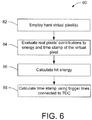
- FIGURE 6 illustrates a method 80 of using a hardware-based virtual pixel to facilitate combining smaller real pixels.
- a hardware-based virtual pixel is employed, which comprises a plurality of smaller real pixels, such as is described with regard to Figures 2 and 3 , above.
- contributions of each real pixel to total energy and time stamp of the virtual pixel are evaluated.
- the total energy registered at the virtual pixels is calculated, such as by summing the energies of all real pixels in the virtual pixel.
- the time stamp for a gamma ray hit is determined using hardwired trigger lines and a TDC and component. For instance, since all pixels comprised by the hard virtual pixel have trigger lines connected through a balanced network connected to a TDC, all pixels can contribute directly to the time stamp of the hit.
- Anger logic can be employed to facilitate using a standard chip with a given crystal size for larger or smaller scanning applications.
- a photodetector chip can be optimized for a scanner with 2x2mm 2 crystals, and same chip can be used in a full-body scanner, if four 2x2 pixels are combined to realize a 4x4mm 2 virtual pixel with timing resolution optimized for TOF.
- the same detector chip can be connected to a light guide and 1x1mm 2 crystals, for example in an animal scanner.
- the 2x2mm 2 chip can be coupled to 1x1mm 2 crystals in a mapping such as is described above with regard to Figure 4 .
- the circuitry implementing the Anger logic can be placed on the same chip, thus making the type of readout transparent to the rest of the system.
- the orientation of the photodetector pixels building a virtual pixel can be optimized to minimize the dead area due to the electronics, as shown in Figure 3 , above.
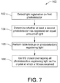
- FIGURE 7 illustrates a method 100 of enabling a quasi-pixelated readout scheme and reducing readout channels for a detector comprising photodetectors directly coupled to a number of scintillation crystals, such as detector 50 described above.
- the crystals have a pitch one-half the size of the pitch of the photodetectors to which they are coupled.
- a hit is detected on a first photodetector.
- a determination is made regarding whether a second photodetector, adjacent to the first photo detector, has registered a hit comprising a substantially equal amount of light.
- a table lookup is performed for all adjacent photodetectors registering substantially equal hits, in order to determine where the hit was received.
- a crystal that received the hit is identified based on the photodetectors that registered the substantially equal hits.
- a first photodetector registers a hit at 102 and no second photodetector registers a hit per the determination at 104.
- a lookup of the table at 106 results in an identification of a single crystal at 108, which is the crystal that is coupled solely to the first photodetector and does not overlay any other photodetectors.
- the lookup at 106 will result in an identification, at 108, of the crystal that overlaps both of the photodetectors and no other photodetector.
- four photodetectors register substantially equal hits as determined at 102 and 104. In this case, the lookup at 106 will identify the crystal that overlaps a corner of all four photodetectors, at 108.
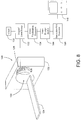
- FIGURE 8 illustrates a diagnostic imaging device 120 such as may be employed in conjunction with one or more of the detectors, detector arrays, pixel arrays, virtual pixels, and/or methods described herein.
- the diagnostic imaging device 120 includes a housing 122 and a subject support 124. Enclosed within the housing 122 is a detector array 126.
- the detector array 126 includes a plurality of individual detector elements 128.
- the array 126 is arranged so that detector elements 128 are distributed evenly about an imaging region 130.
- the detector array 126 can be a ring of detectors 128, multiple rings, or discrete flat panels disposed opposing each other.
- each detector has a plurality of counterpart detectors across the imaging region to facilitate coincidence detection.
- PET positron emission tomography
- pairs of gamma rays are produced by a positron annihilation event in the imaging region and travel in opposite directions. These gamma rays are detected as pairs, with a slight delay (on the order of nanoseconds) between detections if one gamma ray travels farther to reach a detector than the other.
- the radiopharmaceutical contains a radioactive element coupled to a tag molecule.
- the tag molecule is associated with the region to be imaged, and tends to gather there through normal body processes. For example, rapidly multiplying cancer cells tend to expend abnormally high amounts of energy duplicating themselves. So, the radiopharmaceutical can be linked to a molecule, such as glucose that a cell typically metabolizes to create energy, gather in such regions and appear as "hot spots" in the image. Other techniques monitor tagged molecules flowing in the circulatory system.
- the selected radioisotope emits positrons.
- the positron can only move a very short distance (on the order of nanometers) before it is annihilated in an annihilation reaction that creates two oppositely directed gamma rays.
- the pair of gamma rays travel in opposite directions at the speed of light striking an opposing pair of detectors.
- a triggering processor 132 monitors each detector 128 for an energy spike, e.g., integrated area under the pulse, characteristic of the energy of each received gamma ray.
- the triggering processor 132 checks a clock 133 and stamps each detected gamma ray with a time of leading edge receipt stamp.
- the time stamp is first used by an event verification processor 134 to determine which gamma rays are a pair which defines a line of response (LOR).
- gamma rays travel at the speed of light, if detected gamma rays arrive more than several nanoseconds apart, they probably were not generated by the same annihilation event and are discarded. Timing is especially important in TOF-PET, as the minute difference in substantially simultaneous events can be used to further localize the annihilation event along the LOR. As computer processor clock speeds become faster, the higher the accuracy with which an event can be localized along its LOR. In a SPECT camera, the LOR or trajectory for each detected gamma ray is determined by collimation.
- LORs are stored in an event storage buffer 144, and a reconstruction processor 146 reconstructs the LORs into an image representation of the subject using filtered backprojection or other appropriate reconstruction algorithm.
- the reconstruction can then be displayed for a user on a display device 148, printed, saved for later use, and the like.
Claims (5)
- Virtuelles Pixel-Array für ein System zur diagnostischen Bildgebung, das Folgendes umfasst:ein virtuelles Pixel umfassend mindestens ein Szintillatorkristall (10);eine Vielzahl von optisch mit dem Szintillatorkristall (10) gekoppelten Photodetektoren (12), die konfiguriert sind, um in Reaktion auf die Szintillationen in dem Kristall Ausgangssignale zu erzeugen; undeine Virtualisierungseinheit (14), die konfiguriert ist, um die zu einem Gammastrahlaufprall auf das Szintillatorkristall, wie er durch die Vielzahl von Photodetektoren erkannt wird, gehörenden Ausgangssignale zu verarbeiten und einen Zeitstempel für jeden Gammastrahlaufprall zu berechnen;wobei das virtuelle Pixel ein software-basiertes Pixel ist und die Virtualisierungseinheit (14) einen Algorithmus nutzt, der konfiguriert ist, um die Gesamtenergie des Gammastrahlaufpralls durch Kombinieren der Energien zu berechnen, die durch die Vielzahl von Photodetektoren (12), welche zu dem Gammastrahlaufprall gehören, detektiert werden, und wobei der Algorithmus weiterhin konfiguriert ist, um den Zeitstempel zu berechnen;
dadurch gekennzeichnet, dass die Virtualisierungseinheit (14) entweder:i) konfiguriert ist, um den Zeitstempel als eine energie-gewichtete Summe eines partiellen Photodetektor-Zeitstempels anhand der Ausgangssignale von jedem der Vielzahl von Photodetektoren (12) zu berechnen; oderii) konfiguriert ist, um den Zeitstempel als eine Funktion des Ausgangssignals eines Photodetektors (12) zu berechnen, der ein höchstes Energieniveau relativ zu anderen Photodetektoren (12) in dem virtuellen Pixel registriert. - System nach Anspruch 1, wobei die Vielzahl von Photodetektoren (12) vier Photodetektoren umfasst, die in einem 2x2-Array angeordnet sind.
- System nach Anspruch 2, das weiterhin Folgendes umfasst:eine Vielzahl von Szintillatorkristallen, die in einem rechteckigen Raster angeordnet sind;eine Vielzahl von 2x2-Arrays von Photodetektoren, die optisch mit den Szintillatorkristallen in einer Versatzbeziehung derartig gekoppelt sind, dass in jedem 2x2-Array einer der Photodetektoren optisch mit nur einem Szintillatorkristall gekoppelt ist, einer der Photodetektoren optisch mit zwei der Szintillatorkristalle gekoppelt ist und zwei der Photodetektoren optisch mit vier der Szintillatorkristalle gekoppelt sind.
- Verfahren zum Berechnen eines Zeitstempels für ein virtuelles Pixel, einschließlich:Empfangen eines Gammastrahlaufpralls auf ein Szintillatorkristall (10) des virtuellen Pixels;Evaluieren von Ausgangssignalen von jedem von einer Vielzahl von Photodetektoren (12), die optisch mit dem Szintillatorkristall gekoppelt sind, um eine Energie und einen Photodetektor-Zeitstempel für jeden zu dem Gammastrahlaufprall gehörenden Photodetektor zu ermitteln;Berechnen einer Gesamtenergie des Gammastrahlaufpralls durch Kombinieren der Energien, die durch die Vielzahl von Photodetektoren (12), welche zu dem Gammastrahlaufprall gehören, detektiert werden; undBerechnen eines Zeitstempels für den Gammastrahlaufprall als eine Funktion des durch mindestens einen Photodetektor (12) in der Vielzahl von Photodetektoren registrierten Photodetektor-Zeitstempels;gekennzeichnet durch entweder:i) Berechnen des Zeitstempels für den Gammastrahlaufprall als eine energie-gewichtete Summe eines partiellen Photodetektor-Zeitstempels anhand von jedem der Vielzahl von Photodetektoren (12), die zu dem Gammastrahlaufprall gehören; oderii) Berechnen des Zeitstempels als eine Funktion eines Photodetektor-Zeitstempels eines Photodetektors (12), der ein höchstes Energieniveau relativ zu anderen Photodetektoren in dem virtuellen Pixel registriert.
- Verfahren nach Anspruch 4, weiterhin umfassend das Berechnen des Zeitstempels als eine Funktion von partiellen Zeitstempeln, die bei einem Zeit-zu-Digitalwanderl (26) über ein Netzwerk empfangen werden, das eine Triggerleitung von jedem der Vielzahl von Photodetektoren verbindet.
Applications Claiming Priority (2)
| Application Number | Priority Date | Filing Date | Title |
|---|---|---|---|
| US93828207P | 2007-05-16 | 2007-05-16 | |
| PCT/IB2008/051663 WO2008142590A2 (en) | 2007-05-16 | 2008-04-29 | Virtual pet detector and quasi-pixelated readout scheme for pet |
Publications (2)
| Publication Number | Publication Date |
|---|---|
| EP2162762A2 EP2162762A2 (de) | 2010-03-17 |
| EP2162762B1 true EP2162762B1 (de) | 2016-06-08 |
Family
ID=40032243
Family Applications (1)
| Application Number | Title | Priority Date | Filing Date |
|---|---|---|---|
| EP08738026.7A Active EP2162762B1 (de) | 2007-05-16 | 2008-04-29 | Virtueller pet-detektor und quasi-gepixeltes ableseschema für pet |
Country Status (6)
| Country | Link |
|---|---|
| US (2) | US9423511B2 (de) |
| EP (1) | EP2162762B1 (de) |
| JP (1) | JP5641930B2 (de) |
| CN (2) | CN101680953B (de) |
| RU (1) | RU2473099C2 (de) |
| WO (1) | WO2008142590A2 (de) |
Families Citing this family (41)
| Publication number | Priority date | Publication date | Assignee | Title |
|---|---|---|---|---|
| US8410451B2 (en) | 2009-04-09 | 2013-04-02 | Boss Physical Sciences Llc | Neutron fluorescence with synchronized gamma detector |
| JP5413019B2 (ja) * | 2009-07-27 | 2014-02-12 | 大日本印刷株式会社 | 放射線画像処理装置、放射線画像処理方法及び放射線画像処理プログラム |
| WO2011037945A2 (en) | 2009-09-22 | 2011-03-31 | Boss Physical Sciences Llc | Organic-scintillator compton gamma ray telescope |
| RU2567400C2 (ru) * | 2010-08-26 | 2015-11-10 | Конинклейке Филипс Электроникс Н.В. | Пикселированное детекторное устройство |
| US8946643B2 (en) * | 2010-10-09 | 2015-02-03 | Fmi Technologies, Inc. | Virtual pixelated detector for pet and/or spect |
| KR101233984B1 (ko) | 2011-04-28 | 2013-02-18 | 서강대학교산학협력단 | 한층 섬광결정을 이용하여 영상을 재구성하는 방법 |
| WO2012152587A2 (en) * | 2011-05-10 | 2012-11-15 | Eberhard-Karls-Universität Tübingen Universitätsklinikum | Gamma detector based on geigermode avalanche photodiodes |
| US9176241B2 (en) | 2011-08-03 | 2015-11-03 | Koninklijke Philips N.V. | Position-sensitive readout modes for digital silicon photomultiplier arrays |
| JP6312606B2 (ja) | 2012-01-31 | 2018-04-18 | ユーティー−バッテル・エルエルシー | 行および列の加算を使用する中性子カメラおよびその操作方法 |
| US8680474B2 (en) * | 2012-03-02 | 2014-03-25 | Luxen Technologies, Inc. | Parallel readout integrated circuit architecture for X-ray image sensor |
| US9140804B2 (en) * | 2012-03-30 | 2015-09-22 | General Electric Company | Methods and systems for determining timing recovery information in a positron emission tomography (PET) system |
| EP2733189B1 (de) * | 2012-11-14 | 2019-10-16 | Koninklijke Philips N.V. | Szintillatormaterial |
| JP6306062B2 (ja) * | 2013-03-08 | 2018-04-04 | コーニンクレッカ フィリップス エヌ ヴェKoninklijke Philips N.V. | 検出された放射量子のタイムスタンピング |
| WO2014180487A1 (en) * | 2013-05-07 | 2014-11-13 | Cern - European Organization For Nuclear Research | A detector configuration with semiconductor photomultiplier strips and differential readout |
| CN104656115B (zh) * | 2013-11-19 | 2018-04-24 | 苏州瑞派宁科技有限公司 | 一种时间标记组合的方法与系统 |
| CN104116519B (zh) * | 2014-07-30 | 2016-09-07 | 西安电子科技大学 | 基于多边形视野对称性的旋转双平板pet系统及其成像方法 |
| CN105655435B (zh) | 2014-11-14 | 2018-08-07 | 苏州瑞派宁科技有限公司 | 光电转换器、探测器及扫描设备 |
| CN104570042B (zh) * | 2014-12-11 | 2017-10-03 | 沈阳东软医疗系统有限公司 | 一种核探测器晶体位置的识别方法和装置 |
| CN104539243B (zh) * | 2014-12-12 | 2017-11-21 | 北京永新医疗设备有限公司 | 伽玛射线的位置读出装置和伽玛射线的位置读出系统 |
| US9606245B1 (en) | 2015-03-24 | 2017-03-28 | The Research Foundation For The State University Of New York | Autonomous gamma, X-ray, and particle detector |
| JP6454612B2 (ja) * | 2015-06-24 | 2019-01-16 | 株式会社リガク | X線データ処理装置、その方法およびプログラム |
| CN105182401B (zh) | 2015-09-30 | 2019-05-21 | 东软医疗系统股份有限公司 | 一种核探测器晶体位置识别装置 |
| CN105590029B (zh) * | 2015-12-23 | 2018-07-10 | 中国科学院深圳先进技术研究院 | 一种基于双端探测器的晶体分辨图计算方法和装置 |
| US10686003B2 (en) * | 2015-12-31 | 2020-06-16 | General Electric Company | Radiation detector assembly |
| ES2672118B1 (es) * | 2016-10-25 | 2019-03-28 | General Equipment For Medical Imaging S A | Metodo de generacion de imagenes nucleares para dispositivos de imagen nuclear con detectores de cristal continuo |
| JP6822859B2 (ja) | 2017-01-24 | 2021-01-27 | キヤノンメディカルシステムズ株式会社 | 検出装置及び検出方法 |
| WO2019041172A1 (en) * | 2017-08-30 | 2019-03-07 | Shenzhen United Imaging Healthcare Co., Ltd. | SYSTEM, METHOD AND DETECTOR MODULE FOR PET IMAGING |
| CN107440734B (zh) * | 2017-09-04 | 2020-12-01 | 东软医疗系统股份有限公司 | 一种pet扫描方法和装置 |
| US10775516B2 (en) | 2017-10-24 | 2020-09-15 | Saint-Gobain Ceramics & Plastics, Inc. | Radiation detection apparatus having an analyzer within a housing |
| CN108926356B (zh) * | 2018-05-31 | 2022-03-25 | 上海联影医疗科技股份有限公司 | 探测器光子到达信息确定方法、装置和医疗设备 |
| EP3887867A4 (de) | 2018-11-30 | 2022-11-02 | Saint-Gobain Ceramics & Plastics Inc. | Strahlungsdetektor mit reflektor |
| CN109884682B (zh) * | 2019-02-01 | 2020-12-01 | 东软医疗系统股份有限公司 | 一种晶体位置查找表的生成方法、装置、设备及介质 |
| EP3924754A4 (de) | 2019-02-15 | 2022-12-07 | The Research Foundation for The State University of New York | Hochauflösender tiefencodierender pet-detektor mit prismatoidem lichtleiterarray |
| US11039801B2 (en) * | 2019-07-02 | 2021-06-22 | GE Precision Healthcare LLC | Systems and methods for high-resolution spectral computed tomography imaging |
| CN110426730B (zh) * | 2019-07-19 | 2022-11-01 | 东软医疗系统股份有限公司 | 信号读出电路、信号读出方法及装置 |
| CN110403622B (zh) * | 2019-07-23 | 2023-03-21 | 上海联影医疗科技股份有限公司 | 生成查找表的寻峰方法、装置、计算机设备和存储介质 |
| CN110596725B (zh) * | 2019-09-19 | 2022-03-04 | 深圳奥锐达科技有限公司 | 基于插值的飞行时间测量方法及测量系统 |
| ES2843924B2 (es) * | 2020-01-20 | 2024-01-02 | Univ Valencia Politecnica | Dispositivo para la deteccion de rayos gamma con codificacion de profundidad de interaccion y tiempo de vuelo |
| DE102020120788B3 (de) | 2020-08-06 | 2021-12-09 | Helmholtz-Zentrum Dresden - Rossendorf E. V. | Multipixel-photodetektor mit avalanche-photodioden, strahlungsdetektor und positronen-emissions-tomograph |
| JP2022077085A (ja) * | 2020-11-11 | 2022-05-23 | キヤノンメディカルシステムズ株式会社 | 放射線検出器 |
| JP2023161476A (ja) * | 2022-04-25 | 2023-11-07 | キヤノンメディカルシステムズ株式会社 | Pet装置、画像処理方法及びプログラム |
Citations (1)
| Publication number | Priority date | Publication date | Assignee | Title |
|---|---|---|---|---|
| US6169285B1 (en) * | 1998-10-23 | 2001-01-02 | Adac Laboratories | Radiation-based imaging system employing virtual light-responsive elements |
Family Cites Families (33)
| Publication number | Priority date | Publication date | Assignee | Title |
|---|---|---|---|---|
| US4560882A (en) * | 1984-08-31 | 1985-12-24 | Regents Of The University Of California | High-efficiency X-radiation converters |
| US4864140A (en) * | 1987-08-31 | 1989-09-05 | The University Of Michigan | Coincidence detection system for positron emission tomography |
| US5319204A (en) * | 1992-05-13 | 1994-06-07 | Board Of Regents, The University Of Texas System | Positron emission tomography camera with quadrant-sharing photomultipliers and cross-coupled scintillating crystals |
| US5391879A (en) * | 1993-11-19 | 1995-02-21 | Minnesota Mining And Manufacturing Company | Radiation detector |
| DE69528949T2 (de) * | 1994-10-03 | 2003-08-28 | Koninkl Philips Electronics Nv | Verbessertes Gammakamera-System |
| US5715292A (en) * | 1994-11-25 | 1998-02-03 | Loral Fairchild Corporation | Digital sensor cassette for mammography |
| EP0958508B1 (de) * | 1997-02-10 | 2007-03-28 | THE UNIVERSITY OF ALBERTA, SIMON FRASER UNIVERSITY, THE UNIV. OF VICTORIA,THE UNIV. OF BRITISH COLUMBIA, carrying on as TRIUMF | Unterteilter szintillationsdetektor zur feststellung der koordinaten von photoneninteraktionen |
| TW541184B (en) * | 1997-04-30 | 2003-07-11 | Univ Leland Stanford Junior | Use of annexin for imaging cell death in vivo |
| US6114703A (en) * | 1997-10-21 | 2000-09-05 | The Regents Of The University Of California | High resolution scintillation detector with semiconductor readout |
| JPH11128214A (ja) * | 1997-10-30 | 1999-05-18 | Shimadzu Corp | X線診断装置 |
| EP1040650B1 (de) * | 1997-12-18 | 2001-07-04 | Simage Oy | Vorrichtung zur strahlungsbildaufnahme |
| US6362479B1 (en) * | 1998-03-25 | 2002-03-26 | Cti Pet Systems, Inc. | Scintillation detector array for encoding the energy, position, and time coordinates of gamma ray interactions |
| US6678411B1 (en) * | 1999-06-04 | 2004-01-13 | Look Dynamics, Inc. | Apparatus and method for characterizing, encoding, storing, and searching images by shape |
| US6437338B1 (en) * | 1999-09-29 | 2002-08-20 | General Electric Company | Method and apparatus for scanning a detector array in an x-ray imaging system |
| GB0029430D0 (en) * | 2000-12-04 | 2001-01-17 | Univ Leicester | Devices for imaging radionuclide emissions |
| JP2002181938A (ja) * | 2000-12-19 | 2002-06-26 | Shimadzu Corp | 放射線検出器 |
| US6393097B1 (en) * | 2000-12-22 | 2002-05-21 | Ge Medical Systems Global Technology Company, Llc | Digital detector method for dual energy imaging |
| JP2002207080A (ja) * | 2001-01-10 | 2002-07-26 | Shimadzu Corp | 放射線検出器 |
| IL143980A0 (en) * | 2001-06-25 | 2002-04-21 | Imarad Imaging Systems Ltd | Three dimensional radiation detection |
| US6510195B1 (en) * | 2001-07-18 | 2003-01-21 | Koninklijke Philips Electronics, N.V. | Solid state x-radiation detector modules and mosaics thereof, and an imaging method and apparatus employing the same |
| JP2003050280A (ja) * | 2001-08-03 | 2003-02-21 | Konica Corp | 放射線画像検出器 |
| AU2003217283A1 (en) * | 2002-02-01 | 2003-10-08 | Board Of Regents, The University Of Texas System | A production method for making position-sensitive radiation detector arrays |
| US6868138B2 (en) * | 2002-05-29 | 2005-03-15 | The Regents Of The University Of Michigan | Method, processor and computed tomography (CT) machine for generating images utilizing high and low sensitivity data collected from a flat panel detector having an extended dynamic range |
| US6885827B2 (en) * | 2002-07-30 | 2005-04-26 | Amplification Technologies, Inc. | High sensitivity, high resolution detection of signals |
| DE10307752B4 (de) * | 2003-02-14 | 2007-10-11 | Siemens Ag | Röntgendetektor |
| US7164136B2 (en) * | 2003-10-07 | 2007-01-16 | Siemens Medical Solutions Usa, Inc. | Detector array using a continuous light guide |
| US20050098732A1 (en) * | 2003-11-10 | 2005-05-12 | Ls Technologies, Inc. | Flat-panel detector utilizing electrically interconnecting tiled photosensor arrays |
| EP1709462A1 (de) * | 2004-01-15 | 2006-10-11 | Koninklijke Philips Electronics N.V. | Über eine nachschlagetabelle erzielte ereignis-positionsbestimmung |
| WO2006018766A2 (en) * | 2004-08-13 | 2006-02-23 | Koninklijke Philips Electronics, N.V. | Timing calibration for a tof-pet scanner |
| US20060131508A1 (en) * | 2004-12-22 | 2006-06-22 | Burr Kent C | Systems and methods for improving position resolution of charge-sharing position sensitive detectors |
| JP5623700B2 (ja) * | 2005-04-22 | 2014-11-12 | コーニンクレッカ フィリップス エヌ ヴェ | 飛行時間能力を有するpet/mriスキャナ |
| ATE514105T1 (de) * | 2005-04-22 | 2011-07-15 | Koninkl Philips Electronics Nv | Digitaler silicium-photovervielfacher für ein tof-pet |
| JP4877766B2 (ja) * | 2006-08-25 | 2012-02-15 | 独立行政法人放射線医学総合研究所 | 陽電子放射断層撮像装置及び放射線検出器 |
-
2008
- 2008-04-29 RU RU2009146553/28A patent/RU2473099C2/ru not_active IP Right Cessation
- 2008-04-29 JP JP2010508010A patent/JP5641930B2/ja active Active
- 2008-04-29 EP EP08738026.7A patent/EP2162762B1/de active Active
- 2008-04-29 CN CN200880015943.4A patent/CN101680953B/zh active Active
- 2008-04-29 CN CN201410330669.7A patent/CN104076383B/zh active Active
- 2008-04-29 US US12/600,072 patent/US9423511B2/en active Active
- 2008-04-29 WO PCT/IB2008/051663 patent/WO2008142590A2/en active Application Filing
-
2016
- 2016-07-14 US US15/209,842 patent/US11119227B2/en active Active
Patent Citations (1)
| Publication number | Priority date | Publication date | Assignee | Title |
|---|---|---|---|---|
| US6169285B1 (en) * | 1998-10-23 | 2001-01-02 | Adac Laboratories | Radiation-based imaging system employing virtual light-responsive elements |
Also Published As
| Publication number | Publication date |
|---|---|
| CN104076383B (zh) | 2017-08-15 |
| US20160320496A1 (en) | 2016-11-03 |
| US20100219345A1 (en) | 2010-09-02 |
| US9423511B2 (en) | 2016-08-23 |
| WO2008142590A3 (en) | 2009-08-06 |
| RU2473099C2 (ru) | 2013-01-20 |
| JP2010527021A (ja) | 2010-08-05 |
| EP2162762A2 (de) | 2010-03-17 |
| CN101680953A (zh) | 2010-03-24 |
| US11119227B2 (en) | 2021-09-14 |
| RU2009146553A (ru) | 2011-06-27 |
| CN101680953B (zh) | 2014-08-13 |
| WO2008142590A2 (en) | 2008-11-27 |
| CN104076383A (zh) | 2014-10-01 |
| JP5641930B2 (ja) | 2014-12-17 |
Similar Documents
| Publication | Publication Date | Title |
|---|---|---|
| US11119227B2 (en) | Virtual pet detector and quasi-pixelated readout scheme for pet | |
| EP1875271B1 (de) | Digitaler silicium-photovervielfacher für ein tof-pet | |
| RU2543544C2 (ru) | Рет-детекторная система с улучшенными характеристиками количественной оценки | |
| US7601963B2 (en) | High-resolution depth-of-interaction PET detector | |
| EP3153889B1 (de) | Strahlungsdetektionsvorrichtung und strahlungserkennungsverfahren für eine nuklearmedizinische diagnostikvorrichtung | |
| US7193208B1 (en) | Time-of-flight capable high resolution pet detector | |
| US8530846B2 (en) | Apparatus and methods for detector scatter recovery for nuclear medicine imaging systems | |
| EP1627239B1 (de) | Detektormodul zur erfassung von ionisierender strahlung | |
| Lewellen | The challenge of detector designs for PET | |
| US9069089B2 (en) | Methods and systems for increasing the sensitivity of simultaneous multi-isotope positron emission tomography | |
| US7956331B2 (en) | Scintillation detector for positron emission tomography | |
| US9182506B2 (en) | Methods and systems for signal communication in gamma ray detectors | |
| US8466418B2 (en) | Gamma ray detector, radiation diagnostic device, tomography device, and method of analyzing tomography device | |
| JP6257928B2 (ja) | ガンマ線検出器 | |
| JP2005043104A (ja) | 放射線位置検出器の校正方法 | |
| CN106461792B (zh) | 在辐射粒子探测器中的闪烁事件定位 | |
| CN107874773B (zh) | 光子检测方法、装置、设备和系统及存储介质 | |
| US7253415B2 (en) | Method and apparatus for vetoing random coincidences in positron emission tomographs | |
| US20040159791A1 (en) | Pet/spect nuclear scanner | |
| EP4095565A1 (de) | Vorrichtung zur detektion von gammastrahlen mit wechselwirkungstiefe und flugzeitcodierung | |
| US20230236328A1 (en) | Method and apparatus for improved photosensor light collection in a radiation detector | |
| JP2017166863A (ja) | 放射線検出器およびそれを備えたtof−pet装置 |
Legal Events
| Date | Code | Title | Description |
|---|---|---|---|
| PUAI | Public reference made under article 153(3) epc to a published international application that has entered the european phase |
Free format text: ORIGINAL CODE: 0009012 |
|
| 17P | Request for examination filed |
Effective date: 20100208 |
|
| AK | Designated contracting states |
Kind code of ref document: A2 Designated state(s): AT BE BG CH CY CZ DE DK EE ES FI FR GB GR HR HU IE IS IT LI LT LU LV MC MT NL NO PL PT RO SE SI SK TR |
|
| AX | Request for extension of the european patent |
Extension state: AL BA MK RS |
|
| 17Q | First examination report despatched |
Effective date: 20110531 |
|
| DAX | Request for extension of the european patent (deleted) | ||
| RAP1 | Party data changed (applicant data changed or rights of an application transferred) |
Owner name: PHILIPS INTELLECTUAL PROPERTY & STANDARDS GMBH Owner name: KONINKLIJKE PHILIPS N.V. |
|
| GRAP | Despatch of communication of intention to grant a patent |
Free format text: ORIGINAL CODE: EPIDOSNIGR1 |
|
| INTG | Intention to grant announced |
Effective date: 20151217 |
|
| GRAS | Grant fee paid |
Free format text: ORIGINAL CODE: EPIDOSNIGR3 |
|
| GRAA | (expected) grant |
Free format text: ORIGINAL CODE: 0009210 |
|
| AK | Designated contracting states |
Kind code of ref document: B1 Designated state(s): AT BE BG CH CY CZ DE DK EE ES FI FR GB GR HR HU IE IS IT LI LT LU LV MC MT NL NO PL PT RO SE SI SK TR |
|
| REG | Reference to a national code |
Ref country code: GB Ref legal event code: FG4D |
|
| REG | Reference to a national code |
Ref country code: CH Ref legal event code: EP |
|
| REG | Reference to a national code |
Ref country code: IE Ref legal event code: FG4D |
|
| REG | Reference to a national code |
Ref country code: AT Ref legal event code: REF Ref document number: 805631 Country of ref document: AT Kind code of ref document: T Effective date: 20160715 |
|
| REG | Reference to a national code |
Ref country code: DE Ref legal event code: R096 Ref document number: 602008044609 Country of ref document: DE |
|
| REG | Reference to a national code |
Ref country code: LT Ref legal event code: MG4D |
|
| REG | Reference to a national code |
Ref country code: NL Ref legal event code: MP Effective date: 20160608 |
|
| PG25 | Lapsed in a contracting state [announced via postgrant information from national office to epo] |
Ref country code: FI Free format text: LAPSE BECAUSE OF FAILURE TO SUBMIT A TRANSLATION OF THE DESCRIPTION OR TO PAY THE FEE WITHIN THE PRESCRIBED TIME-LIMIT Effective date: 20160608 Ref country code: NO Free format text: LAPSE BECAUSE OF FAILURE TO SUBMIT A TRANSLATION OF THE DESCRIPTION OR TO PAY THE FEE WITHIN THE PRESCRIBED TIME-LIMIT Effective date: 20160908 Ref country code: LT Free format text: LAPSE BECAUSE OF FAILURE TO SUBMIT A TRANSLATION OF THE DESCRIPTION OR TO PAY THE FEE WITHIN THE PRESCRIBED TIME-LIMIT Effective date: 20160608 |
|
| REG | Reference to a national code |
Ref country code: AT Ref legal event code: MK05 Ref document number: 805631 Country of ref document: AT Kind code of ref document: T Effective date: 20160608 |
|
| PG25 | Lapsed in a contracting state [announced via postgrant information from national office to epo] |
Ref country code: HR Free format text: LAPSE BECAUSE OF FAILURE TO SUBMIT A TRANSLATION OF THE DESCRIPTION OR TO PAY THE FEE WITHIN THE PRESCRIBED TIME-LIMIT Effective date: 20160608 Ref country code: LV Free format text: LAPSE BECAUSE OF FAILURE TO SUBMIT A TRANSLATION OF THE DESCRIPTION OR TO PAY THE FEE WITHIN THE PRESCRIBED TIME-LIMIT Effective date: 20160608 Ref country code: ES Free format text: LAPSE BECAUSE OF FAILURE TO SUBMIT A TRANSLATION OF THE DESCRIPTION OR TO PAY THE FEE WITHIN THE PRESCRIBED TIME-LIMIT Effective date: 20160608 Ref country code: NL Free format text: LAPSE BECAUSE OF FAILURE TO SUBMIT A TRANSLATION OF THE DESCRIPTION OR TO PAY THE FEE WITHIN THE PRESCRIBED TIME-LIMIT Effective date: 20160608 Ref country code: SE Free format text: LAPSE BECAUSE OF FAILURE TO SUBMIT A TRANSLATION OF THE DESCRIPTION OR TO PAY THE FEE WITHIN THE PRESCRIBED TIME-LIMIT Effective date: 20160608 Ref country code: GR Free format text: LAPSE BECAUSE OF FAILURE TO SUBMIT A TRANSLATION OF THE DESCRIPTION OR TO PAY THE FEE WITHIN THE PRESCRIBED TIME-LIMIT Effective date: 20160909 |
|
| PG25 | Lapsed in a contracting state [announced via postgrant information from national office to epo] |
Ref country code: IS Free format text: LAPSE BECAUSE OF FAILURE TO SUBMIT A TRANSLATION OF THE DESCRIPTION OR TO PAY THE FEE WITHIN THE PRESCRIBED TIME-LIMIT Effective date: 20161008 Ref country code: RO Free format text: LAPSE BECAUSE OF FAILURE TO SUBMIT A TRANSLATION OF THE DESCRIPTION OR TO PAY THE FEE WITHIN THE PRESCRIBED TIME-LIMIT Effective date: 20160608 Ref country code: SK Free format text: LAPSE BECAUSE OF FAILURE TO SUBMIT A TRANSLATION OF THE DESCRIPTION OR TO PAY THE FEE WITHIN THE PRESCRIBED TIME-LIMIT Effective date: 20160608 Ref country code: CZ Free format text: LAPSE BECAUSE OF FAILURE TO SUBMIT A TRANSLATION OF THE DESCRIPTION OR TO PAY THE FEE WITHIN THE PRESCRIBED TIME-LIMIT Effective date: 20160608 Ref country code: EE Free format text: LAPSE BECAUSE OF FAILURE TO SUBMIT A TRANSLATION OF THE DESCRIPTION OR TO PAY THE FEE WITHIN THE PRESCRIBED TIME-LIMIT Effective date: 20160608 |
|
| PG25 | Lapsed in a contracting state [announced via postgrant information from national office to epo] |
Ref country code: PT Free format text: LAPSE BECAUSE OF FAILURE TO SUBMIT A TRANSLATION OF THE DESCRIPTION OR TO PAY THE FEE WITHIN THE PRESCRIBED TIME-LIMIT Effective date: 20161010 Ref country code: BE Free format text: LAPSE BECAUSE OF FAILURE TO SUBMIT A TRANSLATION OF THE DESCRIPTION OR TO PAY THE FEE WITHIN THE PRESCRIBED TIME-LIMIT Effective date: 20160608 Ref country code: PL Free format text: LAPSE BECAUSE OF FAILURE TO SUBMIT A TRANSLATION OF THE DESCRIPTION OR TO PAY THE FEE WITHIN THE PRESCRIBED TIME-LIMIT Effective date: 20160608 Ref country code: AT Free format text: LAPSE BECAUSE OF FAILURE TO SUBMIT A TRANSLATION OF THE DESCRIPTION OR TO PAY THE FEE WITHIN THE PRESCRIBED TIME-LIMIT Effective date: 20160608 |
|
| REG | Reference to a national code |
Ref country code: DE Ref legal event code: R097 Ref document number: 602008044609 Country of ref document: DE |
|
| PLBE | No opposition filed within time limit |
Free format text: ORIGINAL CODE: 0009261 |
|
| STAA | Information on the status of an ep patent application or granted ep patent |
Free format text: STATUS: NO OPPOSITION FILED WITHIN TIME LIMIT |
|
| REG | Reference to a national code |
Ref country code: FR Ref legal event code: PLFP Year of fee payment: 10 |
|
| 26N | No opposition filed |
Effective date: 20170309 |
|
| PG25 | Lapsed in a contracting state [announced via postgrant information from national office to epo] |
Ref country code: DK Free format text: LAPSE BECAUSE OF FAILURE TO SUBMIT A TRANSLATION OF THE DESCRIPTION OR TO PAY THE FEE WITHIN THE PRESCRIBED TIME-LIMIT Effective date: 20160608 Ref country code: SI Free format text: LAPSE BECAUSE OF FAILURE TO SUBMIT A TRANSLATION OF THE DESCRIPTION OR TO PAY THE FEE WITHIN THE PRESCRIBED TIME-LIMIT Effective date: 20160608 |
|
| REG | Reference to a national code |
Ref country code: CH Ref legal event code: PL |
|
| REG | Reference to a national code |
Ref country code: IE Ref legal event code: MM4A |
|
| PG25 | Lapsed in a contracting state [announced via postgrant information from national office to epo] |
Ref country code: MC Free format text: LAPSE BECAUSE OF FAILURE TO SUBMIT A TRANSLATION OF THE DESCRIPTION OR TO PAY THE FEE WITHIN THE PRESCRIBED TIME-LIMIT Effective date: 20160608 |
|
| PG25 | Lapsed in a contracting state [announced via postgrant information from national office to epo] |
Ref country code: LU Free format text: LAPSE BECAUSE OF NON-PAYMENT OF DUE FEES Effective date: 20170429 Ref country code: CH Free format text: LAPSE BECAUSE OF NON-PAYMENT OF DUE FEES Effective date: 20170430 Ref country code: LI Free format text: LAPSE BECAUSE OF NON-PAYMENT OF DUE FEES Effective date: 20170430 |
|
| REG | Reference to a national code |
Ref country code: DE Ref legal event code: R082 Ref document number: 602008044609 Country of ref document: DE Representative=s name: MEISSNER BOLTE PATENTANWAELTE RECHTSANWAELTE P, DE Ref country code: DE Ref legal event code: R081 Ref document number: 602008044609 Country of ref document: DE Owner name: PHILIPS GMBH, DE Free format text: FORMER OWNER: PHILIPS INTELLECTUAL PROPERTY & STANDARDS GMBH, 20099 HAMBURG, DE |
|
| PG25 | Lapsed in a contracting state [announced via postgrant information from national office to epo] |
Ref country code: IE Free format text: LAPSE BECAUSE OF NON-PAYMENT OF DUE FEES Effective date: 20170429 |
|
| REG | Reference to a national code |
Ref country code: FR Ref legal event code: PLFP Year of fee payment: 11 |
|
| PGFP | Annual fee paid to national office [announced via postgrant information from national office to epo] |
Ref country code: IT Payment date: 20180424 Year of fee payment: 11 |
|
| PG25 | Lapsed in a contracting state [announced via postgrant information from national office to epo] |
Ref country code: MT Free format text: LAPSE BECAUSE OF NON-PAYMENT OF DUE FEES Effective date: 20170429 |
|
| PG25 | Lapsed in a contracting state [announced via postgrant information from national office to epo] |
Ref country code: HU Free format text: LAPSE BECAUSE OF FAILURE TO SUBMIT A TRANSLATION OF THE DESCRIPTION OR TO PAY THE FEE WITHIN THE PRESCRIBED TIME-LIMIT; INVALID AB INITIO Effective date: 20080429 |
|
| PG25 | Lapsed in a contracting state [announced via postgrant information from national office to epo] |
Ref country code: BG Free format text: LAPSE BECAUSE OF FAILURE TO SUBMIT A TRANSLATION OF THE DESCRIPTION OR TO PAY THE FEE WITHIN THE PRESCRIBED TIME-LIMIT Effective date: 20160608 |
|
| PG25 | Lapsed in a contracting state [announced via postgrant information from national office to epo] |
Ref country code: CY Free format text: LAPSE BECAUSE OF NON-PAYMENT OF DUE FEES Effective date: 20160608 |
|
| PG25 | Lapsed in a contracting state [announced via postgrant information from national office to epo] |
Ref country code: TR Free format text: LAPSE BECAUSE OF FAILURE TO SUBMIT A TRANSLATION OF THE DESCRIPTION OR TO PAY THE FEE WITHIN THE PRESCRIBED TIME-LIMIT Effective date: 20160608 |
|
| PG25 | Lapsed in a contracting state [announced via postgrant information from national office to epo] |
Ref country code: IT Free format text: LAPSE BECAUSE OF NON-PAYMENT OF DUE FEES Effective date: 20190429 |
|
| PGFP | Annual fee paid to national office [announced via postgrant information from national office to epo] |
Ref country code: GB Payment date: 20220419 Year of fee payment: 15 Ref country code: FR Payment date: 20220427 Year of fee payment: 15 |
|
| PGFP | Annual fee paid to national office [announced via postgrant information from national office to epo] |
Ref country code: DE Payment date: 20220628 Year of fee payment: 16 |
|
| GBPC | Gb: european patent ceased through non-payment of renewal fee |
Effective date: 20230429 |
|
| PG25 | Lapsed in a contracting state [announced via postgrant information from national office to epo] |
Ref country code: GB Free format text: LAPSE BECAUSE OF NON-PAYMENT OF DUE FEES Effective date: 20230429 |
|
| PG25 | Lapsed in a contracting state [announced via postgrant information from national office to epo] |
Ref country code: GB Free format text: LAPSE BECAUSE OF NON-PAYMENT OF DUE FEES Effective date: 20230429 Ref country code: FR Free format text: LAPSE BECAUSE OF NON-PAYMENT OF DUE FEES Effective date: 20230430 |