EP2160764B1 - Integrierte schaltung mit einer unteroberflächendiode - Google Patents
Integrierte schaltung mit einer unteroberflächendiode Download PDFInfo
- Publication number
- EP2160764B1 EP2160764B1 EP08732969A EP08732969A EP2160764B1 EP 2160764 B1 EP2160764 B1 EP 2160764B1 EP 08732969 A EP08732969 A EP 08732969A EP 08732969 A EP08732969 A EP 08732969A EP 2160764 B1 EP2160764 B1 EP 2160764B1
- Authority
- EP
- European Patent Office
- Prior art keywords
- region
- integrated circuit
- type
- diode
- substrate
- Prior art date
- Legal status (The legal status is an assumption and is not a legal conclusion. Google has not performed a legal analysis and makes no representation as to the accuracy of the status listed.)
- Not-in-force
Links
Images



Classifications
-
- H—ELECTRICITY
- H10—SEMICONDUCTOR DEVICES; ELECTRIC SOLID-STATE DEVICES NOT OTHERWISE PROVIDED FOR
- H10D—INORGANIC ELECTRIC SEMICONDUCTOR DEVICES
- H10D84/00—Integrated devices formed in or on semiconductor substrates that comprise only semiconducting layers, e.g. on Si wafers or on GaAs-on-Si wafers
-
- H—ELECTRICITY
- H10—SEMICONDUCTOR DEVICES; ELECTRIC SOLID-STATE DEVICES NOT OTHERWISE PROVIDED FOR
- H10D—INORGANIC ELECTRIC SEMICONDUCTOR DEVICES
- H10D84/00—Integrated devices formed in or on semiconductor substrates that comprise only semiconducting layers, e.g. on Si wafers or on GaAs-on-Si wafers
- H10D84/201—Integrated devices formed in or on semiconductor substrates that comprise only semiconducting layers, e.g. on Si wafers or on GaAs-on-Si wafers characterised by the integration of only components covered by H10D1/00 or H10D8/00, e.g. RLC circuits
- H10D84/204—Integrated devices formed in or on semiconductor substrates that comprise only semiconducting layers, e.g. on Si wafers or on GaAs-on-Si wafers characterised by the integration of only components covered by H10D1/00 or H10D8/00, e.g. RLC circuits of combinations of diodes or capacitors or resistors
- H10D84/221—Integrated devices formed in or on semiconductor substrates that comprise only semiconducting layers, e.g. on Si wafers or on GaAs-on-Si wafers characterised by the integration of only components covered by H10D1/00 or H10D8/00, e.g. RLC circuits of combinations of diodes or capacitors or resistors of only diodes
-
- H—ELECTRICITY
- H10—SEMICONDUCTOR DEVICES; ELECTRIC SOLID-STATE DEVICES NOT OTHERWISE PROVIDED FOR
- H10D—INORGANIC ELECTRIC SEMICONDUCTOR DEVICES
- H10D84/00—Integrated devices formed in or on semiconductor substrates that comprise only semiconducting layers, e.g. on Si wafers or on GaAs-on-Si wafers
- H10D84/80—Integrated devices formed in or on semiconductor substrates that comprise only semiconducting layers, e.g. on Si wafers or on GaAs-on-Si wafers characterised by the integration of at least one component covered by groups H10D12/00 or H10D30/00, e.g. integration of IGFETs
- H10D84/811—Combinations of field-effect devices and one or more diodes, capacitors or resistors
-
- H—ELECTRICITY
- H10—SEMICONDUCTOR DEVICES; ELECTRIC SOLID-STATE DEVICES NOT OTHERWISE PROVIDED FOR
- H10D—INORGANIC ELECTRIC SEMICONDUCTOR DEVICES
- H10D89/00—Aspects of integrated devices not covered by groups H10D84/00 - H10D88/00
- H10D89/60—Integrated devices comprising arrangements for electrical or thermal protection, e.g. protection circuits against electrostatic discharge [ESD]
- H10D89/601—Integrated devices comprising arrangements for electrical or thermal protection, e.g. protection circuits against electrostatic discharge [ESD] for devices having insulated gate electrodes, e.g. for IGFETs or IGBTs
- H10D89/611—Integrated devices comprising arrangements for electrical or thermal protection, e.g. protection circuits against electrostatic discharge [ESD] for devices having insulated gate electrodes, e.g. for IGFETs or IGBTs using diodes as protective elements
Definitions
- the present disclosure relates generally to integrated circuits and, more specifically, to a pair of parallel diodes in the integrated circuit.
- Zener or avalanche diodes are used to limit voltages seen by components in an integrated circuit. These diodes are either discrete components external to the integrated circuit or specially integrated into the integrated circuit with the elements they are to protect. Discrete diodes add to the overall costs at the component and the printed circuit board level. Integrated circuit Zener diodes add to the cost by increasing the die area.
- Certain circuits parasitic have intentional inductances that lead to large voltage spikes during fast switching events. Voltage spikes frequently exceed the breakdown of the integrated circuit transistors especially, when the transistors drain to source on-resistance is being minimized. Depending upon the device's architecture, repetitive breakdown events lead to hot carrier charge be trapped. Lateral MOS transistors are particularly susceptible.
- the document US2007/0063274 discloses an overvoltage protective pn juction region formed below an element formation region.
- the document WO2005/117133 discloses ESD protection structures for semiconductor elements comprising at least one semiconductor diode.
- An integrated circuit of the present disclosure as recited in claim 1 includes a first and second diode connected in parallel.
- the first diode has a first breakdown voltage and has first P type region and first N type region adjacent to each other at the surface of the substrate to form a lateral diode.
- the second diode has a second breakdown voltage less than the first breakdown voltage and has a second P type region and second N type region lateral adjacent to each other in the substrate to form a lateral diode below the surface.
- the first and second N type regions overlap and the first and second P type region are electrically connected whereby the first and second diodes are in parallel.
- the second P type and N type regions have a maximum impurity concentration below the surface of the substrate.
- the substrate may include a lateral insulation, for example a trench in the surface, and the second diode is below the trench.
- the first and second P type regions may be spaced in the substrate and are electrically connected by interconnects above the substrate. The first and second P type regions may alternatively overlap to form the electrical connection.
- the first and second P type regions may be a common P type region abutting the first N type region at the surface and the second N type region below the surface.
- the common P type region and the N type region have a maximum impurity concentration below the surface of the substrate.
- the first P type region may be a body of a lateral field effect transistor and the first N type region is a drain region of the field effect transistor.
- the field effect transistor may be an insulated gate field effect transistor.
- Figure 1 is cross-sectional view of an integrated circuit of the prior art.
- Figure 2 is cross-sectional view of an integrated circuit including a pair of parallel diodes according to a first embodiment of the present disclosure.
- Figure 3 is cross-sectional view of the integrated circuit including a pair of parallel diodes according to second and third embodiments of the present disclosure.
- Figure 6 is a table of the repetitive TLP response of eight samples of the devices of Fig. 1-3 .
- Figure 1 illustrates an integrated circuit 10 including a field effect transistor FET 12 of the prior art as an example of an integrated circuit in which the subsurface diode of the present disclosure can be used.
- the integrated circuit includes a substrate 14 shown as a high voltage N type well having a surface 15.
- Field effect transistor 12 includes a P type body region 16 formed in the surface 15 and a P type contact 18 within the P type body 16.
- An N type region 20 is formed in the P body 16 as the source region.
- N type drain region 22 is formed in the surface 15 and spaced from the P body 16 by a surface region 30 of the substrate 14. In some integrated circuits, P type region 16 and N type drain region 22 may overlap.
- An N type drain contact region 24 is formed in the surface 15 of the N type drain region 22.
- the gate 26 extends from the source region 20 across the body region 16 and the adjacent portion of the region 30 of the substrate 14 and onto the drain region 22.
- the structure is a known example of a lateral field effect transistor.
- the cross section is representative of multi drains or fingers of a single field effect transistor or may represent a plurality of parallel field effect transistors.
- the point of breakdown of the field effect transistors is in the region 30 of the substrate 14 between the P body region 16 and the N drain region 22.
- the hot carrier charges are trapped in the gate oxide 28 after repetitive breakdown events. This charge trapping shifts the transistor's parameters over time.
- An avalanche diode 40 may be included in the integrated circuit 10 as illustrated in Figure 2 .
- the transistor's periodicity is broken by the insertion of the avalanche diode 40.
- the avalanche diode 40 includes a P type anode region 42 adjacent and intersecting an N type cathode region 44.
- the cathode region 44 overlaps the drain region 22.
- the anode region 42 includes a P+ anode contact region 46 at the surface 15 of the substrate 14.
- the anode contact region 46 is electrically connected by interconnects 50 with the P contact 18 for the body 16 of the transistor 12. This places the avalanche diode 40 in parallel with the lateral PN diode formed by the body 16 and the drain 22.
- the example in Figure 2 shows trench isolation regions 32 of insulated material at the intersection of the anode region 42 and the cathode region 44. This displaces the breakdown of the avalanche diode 40 below the surface region 15 of the substrate 14.
- the breakdown region is illustrated at 52 at the bottom of the trench region 32.
- the anode region 42 and cathode region 44 are formed as retrograde regions where in the maximum impurity concentration, illustrated by dashed line 48, is below the surface 15 of the substrate 14. This may be formed by ion implantation with subsequent diffusion resulting from the various processing steps.
- the breakdown voltage of the avalanche diode 40 is less than that of the breakdown voltage of the transistor at region 30.
- the structure is two parallel diodes with one of them having a low breakdown voltage and a subsurface breakdown path.
- the reverse breakdown voltage of the avalanche diode 40 will be generally in the range of 12 to 25 volts depending upon the structure of the anode region 42 and the cathode region 44.
- the P+ anode contact 46 can either be embedded into a multi-drain strip arrangement or can be made to the P+ guard ring of the transistor 12 (not shown).
- FIG. 3 Two alternative embodiments are shown in Figure 3 .
- the anode region 42A and the cathode region 44A of diode 40A overlap the body regions 16 and the drain region 22 respectively of transistor 12A. These overlapping regions produce the parallel connection of the two diodes without additional metal interconnects.
- the region 30 of the substrate 14 has a lower impurity concentration, forming a higher voltage junction with the body region 16.
- the higher impurity concentration, low junction voltage anode and cathode regions 42A and 44A intersect and have a breakdown path 52 below the surface.
- the anode region 42A and the cathode region 44A are retrograde regions having their highest impurity concentration at dashed line 48 below the surface 15 of the substrate 14.
- the retrograde regions 42B and 44B are coincidence with and formed not only the avalanche diode's 40B anode and cathode regions but also formed the body and the drain regions of the transistor 12B.
- the avalanche diode breakdowns at 52 is below the surface 15 and conducts carries away from the gate oxide 28. The majority of the avalanche current is swept up through the drain and source body terminals. Since the avalanche current does not interact with the gate oxide, transistor drift is reduced.
- the integrated circuit's maximum concentration will be at approximately 0.5 to 2 microns from the surface 15.
- the embodiments of Figures 2 and 3 have been created using NWELL and PWELL implants which are part of known standard CMOS process as an example. Further device optimization can be achieved by adding dedicated drain/cathode implants and/or body/anode implants.
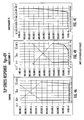
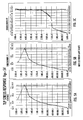
- FIGS 4 through 6 The response of various embodiments compared to the prior art are illustrated in Figures 4 through 6 .
- the control device is that of prior art Figure 1
- embodiment 1 is that of Figure 2
- the embodiment 2 is that of transistor 12B and diode 40B of Figure 3 .
- Figures 4A through 4C and 5A though 5C show the TLP stress response at gate to source voltage of zero and five volts respectively.
- Figure 6 is a table of eight samples that were built and tested for the repetitive TLP stress response at a current of 100 microamperes per 100 nanoseconds every two seconds and a gate to source voltage of 0 volts. The failure of sample 1 of embodiment 2 was not reproducible.
- the subsurface avalanche diode may be used with other diode structures to protect other structures from voltage spikes and specifically repetitive voltage spikes.
Landscapes
- Metal-Oxide And Bipolar Metal-Oxide Semiconductor Integrated Circuits (AREA)
- Insulated Gate Type Field-Effect Transistor (AREA)
Claims (11)
- Integrierte Schaltung, umfassend:ein Substrat mit einer Oberfläche;eine erste Diode mit einer ersten Durchbruchspannung und mit einer ersten P-Typ-Region und einer ersten N-Typ-Region, die an der Oberfläche des Substrats zueinander benachbart sind, um eine laterale Diode zu bilden;eine zweite Diode mit einer zweiten Durchbruchspannung, die kleiner als die erste Durchbruchspannung ist, und mit einer zweiten P-Typ-Region und einer zweiten N-Typ-Region, die in dem Substrat lateral zueinander benachbart sind, um eine laterale Diode unterhalb der Oberfläche zu bilden; undwobei die erste und die zweite N-Typ-Region einander überlappen und die erste und die zweite P-Typ-Region elektrisch verbunden sind, wodurch die erste und die zweite Diode parallel sind.
- Integrierte Schaltung gemäß Anspruch 1, wobei die zweite P-Typ-Region und N-Typ-Region eine maximale Störstellenkonzentration unterhalb der Oberfläche des Substrats haben.
- Integrierte Schaltung gemäß Anspruch 1, wobei das Substrat einen Isolationsgraben in der Oberfläche aufweist und die zweite Diode unterhalb des Grabens liegt.
- Integrierte Schaltung gemäß Anspruch 1, wobei die erste und die zweite P-Typ-Region in dem Substrat beabstandet sind und durch Verbindungen oberhalb des Substrats elelctrisch verbunden sind.
- Integrierte Schaltung gemäß Anspruch 1, wobei die erste und die zweite P-Typ-Region einander überlappen, um die elektrische Verbindung zu bilden.
- Integrierte Schaltung gemäß Anspruch 1, wobei die erste und die zweite P-Typ-Region eine gemeinsame P-Typ-Region sind, die an die erste N-Typ-Region an der Oberfläche und an die zweite N-Typ-Region unterhalb der Oberfläche angrenzt.
- Integrierte Schaltung gemäß Anspruch 6, wobei die gemeinsame P-Typ-Region und die N-Typ-Region eine maximale Störstellenkonzentration unterhalb der Oberfläche des Substrat haben.
- Integrierte Schaltung gemäß Anspruch 1, wobei die erste P-Typ-Region ein Body eines lateralen Feldeffekttransistors ist und die erste N-Typ-Region eine Drain-Region des Feldeffekttransistors ist.
- Integrierte Schaltung gemäß Anspruch 8, wobei der Feldeffekttransistor ein Feldeffekttransistor mit isoliertem Gate ist.
- Integrierte Schaltung gemäß Anspruch 1, wobei die erste P- und die erste N-Typ-Region dieselbe Struktur wie Wannenregionen von lateralen CMOS-Feldeffekttransistoren sind.
- Integrierte Schaltung gemäß Anspruch 1, wobei die zweite Diode eine Durchbruchregion hat und die zweite P- und die zweite N-Typ-Region retrograde Regionen sind, die sich von der Durchbruchregion der zweiten Diode bis benachbart zu der Oberfläche erstrecken.
Applications Claiming Priority (3)
| Application Number | Priority Date | Filing Date | Title |
|---|---|---|---|
| US94545107P | 2007-06-21 | 2007-06-21 | |
| US12/037,569 US7700977B2 (en) | 2007-06-21 | 2008-02-26 | Integrated circuit with a subsurface diode |
| PCT/US2008/058560 WO2008156888A1 (en) | 2007-06-21 | 2008-03-28 | Integrated circuit with a subsurface diode |
Publications (2)
| Publication Number | Publication Date |
|---|---|
| EP2160764A1 EP2160764A1 (de) | 2010-03-10 |
| EP2160764B1 true EP2160764B1 (de) | 2013-01-30 |
Family
ID=40135591
Family Applications (1)
| Application Number | Title | Priority Date | Filing Date |
|---|---|---|---|
| EP08732969A Not-in-force EP2160764B1 (de) | 2007-06-21 | 2008-03-28 | Integrierte schaltung mit einer unteroberflächendiode |
Country Status (6)
| Country | Link |
|---|---|
| US (1) | US7700977B2 (de) |
| EP (1) | EP2160764B1 (de) |
| KR (1) | KR20100031701A (de) |
| CN (1) | CN101681910B (de) |
| TW (1) | TW200901438A (de) |
| WO (1) | WO2008156888A1 (de) |
Families Citing this family (6)
| Publication number | Priority date | Publication date | Assignee | Title |
|---|---|---|---|---|
| US20110121387A1 (en) * | 2009-11-23 | 2011-05-26 | Francois Hebert | Integrated guarded schottky diode compatible with trench-gate dmos, structure and method |
| US20110156682A1 (en) * | 2009-12-30 | 2011-06-30 | Dev Alok Girdhar | Voltage converter with integrated schottky device and systems including same |
| US8492225B2 (en) * | 2009-12-30 | 2013-07-23 | Intersil Americas Inc. | Integrated trench guarded schottky diode compatible with powerdie, structure and method |
| US20110156810A1 (en) * | 2009-12-30 | 2011-06-30 | Intersil Americas Inc. | Integrated dmos and schottky |
| JP2014056989A (ja) | 2012-09-13 | 2014-03-27 | Toshiba Corp | 半導体記憶装置 |
| CN106449634B (zh) * | 2016-09-23 | 2019-06-14 | 矽力杰半导体技术(杭州)有限公司 | 瞬态电压抑制器及其制造方法 |
Citations (2)
| Publication number | Priority date | Publication date | Assignee | Title |
|---|---|---|---|---|
| WO2005117133A2 (de) * | 2004-05-25 | 2005-12-08 | Infineon Technologies Ag | Esd-schutzstrukturen für halbleiterbauelemente |
| US20060043489A1 (en) * | 2004-08-30 | 2006-03-02 | Industrial Technology Research Insititute | Diode and applications thereof |
Family Cites Families (13)
| Publication number | Priority date | Publication date | Assignee | Title |
|---|---|---|---|---|
| JPS6377155A (ja) | 1986-09-19 | 1988-04-07 | Fujitsu Ltd | オ−プンドレイン出力回路 |
| US4736271A (en) * | 1987-06-23 | 1988-04-05 | Signetics Corporation | Protection device utilizing one or more subsurface diodes and associated method of manufacture |
| FR2684240B1 (fr) * | 1991-11-21 | 1994-02-18 | Sgs Thomson Microelectronics Sa | Transistor mos a zener de protection integree. |
| FR2688942A1 (fr) * | 1992-03-20 | 1993-09-24 | Sgs Thomson Microelectronics | Diode a avalanche enterree. |
| JP3173268B2 (ja) * | 1994-01-06 | 2001-06-04 | 富士電機株式会社 | Mis電界効果トランジスタを備えた半導体装置 |
| SE512661C2 (sv) * | 1996-11-13 | 2000-04-17 | Ericsson Telefon Ab L M | Lateral bipolär hybridtransistor med fälteffektmod och förfarande vid densamma |
| JP3090081B2 (ja) * | 1997-03-12 | 2000-09-18 | 日本電気株式会社 | 半導体装置 |
| GB9921071D0 (en) * | 1999-09-08 | 1999-11-10 | Univ Montfort | Insulated base transistor |
| GB9921068D0 (en) * | 1999-09-08 | 1999-11-10 | Univ Montfort | Bipolar mosfet device |
| US7056761B1 (en) * | 2003-03-14 | 2006-06-06 | National Semiconductor Corporation | Avalanche diode with breakdown voltage controlled by gate length |
| US7250668B2 (en) * | 2005-01-20 | 2007-07-31 | Diodes, Inc. | Integrated circuit including power diode |
| JP4785113B2 (ja) * | 2005-02-24 | 2011-10-05 | オンセミコンダクター・トレーディング・リミテッド | 半導体装置 |
| JP4927340B2 (ja) * | 2005-02-24 | 2012-05-09 | オンセミコンダクター・トレーディング・リミテッド | 半導体装置 |
-
2008
- 2008-02-26 US US12/037,569 patent/US7700977B2/en not_active Expired - Fee Related
- 2008-03-27 TW TW097110951A patent/TW200901438A/zh unknown
- 2008-03-28 CN CN2008800209772A patent/CN101681910B/zh not_active Expired - Fee Related
- 2008-03-28 EP EP08732969A patent/EP2160764B1/de not_active Not-in-force
- 2008-03-28 KR KR1020097027435A patent/KR20100031701A/ko not_active Withdrawn
- 2008-03-28 WO PCT/US2008/058560 patent/WO2008156888A1/en not_active Ceased
Patent Citations (2)
| Publication number | Priority date | Publication date | Assignee | Title |
|---|---|---|---|---|
| WO2005117133A2 (de) * | 2004-05-25 | 2005-12-08 | Infineon Technologies Ag | Esd-schutzstrukturen für halbleiterbauelemente |
| US20060043489A1 (en) * | 2004-08-30 | 2006-03-02 | Industrial Technology Research Insititute | Diode and applications thereof |
Also Published As
| Publication number | Publication date |
|---|---|
| KR20100031701A (ko) | 2010-03-24 |
| EP2160764A1 (de) | 2010-03-10 |
| CN101681910A (zh) | 2010-03-24 |
| CN101681910B (zh) | 2011-12-21 |
| US20080315329A1 (en) | 2008-12-25 |
| WO2008156888A1 (en) | 2008-12-24 |
| TW200901438A (en) | 2009-01-01 |
| US7700977B2 (en) | 2010-04-20 |
Similar Documents
| Publication | Publication Date | Title |
|---|---|---|
| US11888047B2 (en) | Lateral transistors and methods with low-voltage-drop shunt to body diode | |
| US7902604B2 (en) | Configuration of gate to drain (GD) clamp and ESD protection circuit for power device breakdown protection | |
| KR100220385B1 (ko) | 정전기 보호 소자 | |
| US7701012B2 (en) | Complementary zener triggered bipolar ESD protection | |
| JP4772843B2 (ja) | 半導体装置及びその製造方法 | |
| JP5703829B2 (ja) | 半導体装置 | |
| US20180090479A1 (en) | Semiconductor Devices and Methods for Forming a Semiconductor Device | |
| EP2160764B1 (de) | Integrierte schaltung mit einer unteroberflächendiode | |
| US9620498B2 (en) | Configuration of gate to drain (GD) clamp and ESD protection circuit for power device breakdown protection | |
| KR101596235B1 (ko) | 와이드 갭 반도체장치 | |
| CN101714575A (zh) | 静电放电保护半导体器件及其制造方法 | |
| KR20130124560A (ko) | 반도체 장치 및 반도체 장치의 제조 방법 | |
| KR100624911B1 (ko) | 정전기 방전 보호 소자 | |
| US7750428B2 (en) | Semiconductor device and method for producing it | |
| KR20160030030A (ko) | 반도체 장치 | |
| US7619280B2 (en) | Current sense trench type MOSFET with improved accuracy and ESD withstand capability | |
| US9748221B2 (en) | Electrostatic discharge protection device and manufacturing method thereof | |
| EP1498956A1 (de) | Halbleiterelement und verfahren zu seiner herstellung | |
| KR100554038B1 (ko) | 반도체 장치 | |
| KR100339426B1 (ko) | 이에스디(esd) 보호회로 | |
| EP3261126A1 (de) | Hochspannungshalbleiterbauelement und verfahren zur herstellung davon | |
| KR19990006882A (ko) | 반도체 장치 | |
| HK1062957A1 (en) | Method of forming a semiconductor device | |
| HK1062957B (en) | Method of forming a semiconductor device |
Legal Events
| Date | Code | Title | Description |
|---|---|---|---|
| PUAI | Public reference made under article 153(3) epc to a published international application that has entered the european phase |
Free format text: ORIGINAL CODE: 0009012 |
|
| 17P | Request for examination filed |
Effective date: 20100121 |
|
| AK | Designated contracting states |
Kind code of ref document: A1 Designated state(s): AT BE BG CH CY CZ DE DK EE ES FI FR GB GR HR HU IE IS IT LI LT LU LV MC MT NL NO PL PT RO SE SI SK TR |
|
| AX | Request for extension of the european patent |
Extension state: AL BA MK RS |
|
| 17Q | First examination report despatched |
Effective date: 20100408 |
|
| DAX | Request for extension of the european patent (deleted) | ||
| REG | Reference to a national code |
Ref country code: DE Ref legal event code: R079 Ref document number: 602008022000 Country of ref document: DE Free format text: PREVIOUS MAIN CLASS: H01L0027080000 Ipc: H01L0027020000 |
|
| GRAP | Despatch of communication of intention to grant a patent |
Free format text: ORIGINAL CODE: EPIDOSNIGR1 |
|
| RIC1 | Information provided on ipc code assigned before grant |
Ipc: H01L 27/08 20060101ALI20121008BHEP Ipc: H01L 27/06 20060101ALI20121008BHEP Ipc: H01L 27/02 20060101AFI20121008BHEP |
|
| GRAS | Grant fee paid |
Free format text: ORIGINAL CODE: EPIDOSNIGR3 |
|
| GRAA | (expected) grant |
Free format text: ORIGINAL CODE: 0009210 |
|
| AK | Designated contracting states |
Kind code of ref document: B1 Designated state(s): AT BE BG CH CY CZ DE DK EE ES FI FR GB GR HR HU IE IS IT LI LT LU LV MC MT NL NO PL PT RO SE SI SK TR |
|
| REG | Reference to a national code |
Ref country code: GB Ref legal event code: FG4D |
|
| REG | Reference to a national code |
Ref country code: CH Ref legal event code: EP |
|
| REG | Reference to a national code |
Ref country code: AT Ref legal event code: REF Ref document number: 595849 Country of ref document: AT Kind code of ref document: T Effective date: 20130215 Ref country code: CH Ref legal event code: EP |
|
| REG | Reference to a national code |
Ref country code: IE Ref legal event code: FG4D |
|
| REG | Reference to a national code |
Ref country code: DE Ref legal event code: R096 Ref document number: 602008022000 Country of ref document: DE Effective date: 20130321 |
|
| REG | Reference to a national code |
Ref country code: AT Ref legal event code: MK05 Ref document number: 595849 Country of ref document: AT Kind code of ref document: T Effective date: 20130130 |
|
| REG | Reference to a national code |
Ref country code: LT Ref legal event code: MG4D |
|
| REG | Reference to a national code |
Ref country code: NL Ref legal event code: VDEP Effective date: 20130130 |
|
| PG25 | Lapsed in a contracting state [announced via postgrant information from national office to epo] |
Ref country code: BG Free format text: LAPSE BECAUSE OF FAILURE TO SUBMIT A TRANSLATION OF THE DESCRIPTION OR TO PAY THE FEE WITHIN THE PRESCRIBED TIME-LIMIT Effective date: 20130430 Ref country code: AT Free format text: LAPSE BECAUSE OF FAILURE TO SUBMIT A TRANSLATION OF THE DESCRIPTION OR TO PAY THE FEE WITHIN THE PRESCRIBED TIME-LIMIT Effective date: 20130130 Ref country code: BE Free format text: LAPSE BECAUSE OF FAILURE TO SUBMIT A TRANSLATION OF THE DESCRIPTION OR TO PAY THE FEE WITHIN THE PRESCRIBED TIME-LIMIT Effective date: 20130130 Ref country code: SE Free format text: LAPSE BECAUSE OF FAILURE TO SUBMIT A TRANSLATION OF THE DESCRIPTION OR TO PAY THE FEE WITHIN THE PRESCRIBED TIME-LIMIT Effective date: 20130130 Ref country code: NO Free format text: LAPSE BECAUSE OF FAILURE TO SUBMIT A TRANSLATION OF THE DESCRIPTION OR TO PAY THE FEE WITHIN THE PRESCRIBED TIME-LIMIT Effective date: 20130430 Ref country code: IS Free format text: LAPSE BECAUSE OF FAILURE TO SUBMIT A TRANSLATION OF THE DESCRIPTION OR TO PAY THE FEE WITHIN THE PRESCRIBED TIME-LIMIT Effective date: 20130530 Ref country code: ES Free format text: LAPSE BECAUSE OF FAILURE TO SUBMIT A TRANSLATION OF THE DESCRIPTION OR TO PAY THE FEE WITHIN THE PRESCRIBED TIME-LIMIT Effective date: 20130511 Ref country code: LT Free format text: LAPSE BECAUSE OF FAILURE TO SUBMIT A TRANSLATION OF THE DESCRIPTION OR TO PAY THE FEE WITHIN THE PRESCRIBED TIME-LIMIT Effective date: 20130130 |
|
| PG25 | Lapsed in a contracting state [announced via postgrant information from national office to epo] |
Ref country code: GR Free format text: LAPSE BECAUSE OF FAILURE TO SUBMIT A TRANSLATION OF THE DESCRIPTION OR TO PAY THE FEE WITHIN THE PRESCRIBED TIME-LIMIT Effective date: 20130501 Ref country code: PT Free format text: LAPSE BECAUSE OF FAILURE TO SUBMIT A TRANSLATION OF THE DESCRIPTION OR TO PAY THE FEE WITHIN THE PRESCRIBED TIME-LIMIT Effective date: 20130530 Ref country code: SI Free format text: LAPSE BECAUSE OF FAILURE TO SUBMIT A TRANSLATION OF THE DESCRIPTION OR TO PAY THE FEE WITHIN THE PRESCRIBED TIME-LIMIT Effective date: 20130130 Ref country code: FI Free format text: LAPSE BECAUSE OF FAILURE TO SUBMIT A TRANSLATION OF THE DESCRIPTION OR TO PAY THE FEE WITHIN THE PRESCRIBED TIME-LIMIT Effective date: 20130130 Ref country code: LV Free format text: LAPSE BECAUSE OF FAILURE TO SUBMIT A TRANSLATION OF THE DESCRIPTION OR TO PAY THE FEE WITHIN THE PRESCRIBED TIME-LIMIT Effective date: 20130130 Ref country code: NL Free format text: LAPSE BECAUSE OF FAILURE TO SUBMIT A TRANSLATION OF THE DESCRIPTION OR TO PAY THE FEE WITHIN THE PRESCRIBED TIME-LIMIT Effective date: 20130130 Ref country code: PL Free format text: LAPSE BECAUSE OF FAILURE TO SUBMIT A TRANSLATION OF THE DESCRIPTION OR TO PAY THE FEE WITHIN THE PRESCRIBED TIME-LIMIT Effective date: 20130130 |
|
| PG25 | Lapsed in a contracting state [announced via postgrant information from national office to epo] |
Ref country code: HR Free format text: LAPSE BECAUSE OF FAILURE TO SUBMIT A TRANSLATION OF THE DESCRIPTION OR TO PAY THE FEE WITHIN THE PRESCRIBED TIME-LIMIT Effective date: 20130130 |
|
| PG25 | Lapsed in a contracting state [announced via postgrant information from national office to epo] |
Ref country code: CZ Free format text: LAPSE BECAUSE OF FAILURE TO SUBMIT A TRANSLATION OF THE DESCRIPTION OR TO PAY THE FEE WITHIN THE PRESCRIBED TIME-LIMIT Effective date: 20130130 Ref country code: DK Free format text: LAPSE BECAUSE OF FAILURE TO SUBMIT A TRANSLATION OF THE DESCRIPTION OR TO PAY THE FEE WITHIN THE PRESCRIBED TIME-LIMIT Effective date: 20130130 Ref country code: MC Free format text: LAPSE BECAUSE OF NON-PAYMENT OF DUE FEES Effective date: 20130331 Ref country code: SK Free format text: LAPSE BECAUSE OF FAILURE TO SUBMIT A TRANSLATION OF THE DESCRIPTION OR TO PAY THE FEE WITHIN THE PRESCRIBED TIME-LIMIT Effective date: 20130130 Ref country code: RO Free format text: LAPSE BECAUSE OF FAILURE TO SUBMIT A TRANSLATION OF THE DESCRIPTION OR TO PAY THE FEE WITHIN THE PRESCRIBED TIME-LIMIT Effective date: 20130130 Ref country code: EE Free format text: LAPSE BECAUSE OF FAILURE TO SUBMIT A TRANSLATION OF THE DESCRIPTION OR TO PAY THE FEE WITHIN THE PRESCRIBED TIME-LIMIT Effective date: 20130130 |
|
| REG | Reference to a national code |
Ref country code: CH Ref legal event code: PL |
|
| PG25 | Lapsed in a contracting state [announced via postgrant information from national office to epo] |
Ref country code: CY Free format text: LAPSE BECAUSE OF FAILURE TO SUBMIT A TRANSLATION OF THE DESCRIPTION OR TO PAY THE FEE WITHIN THE PRESCRIBED TIME-LIMIT Effective date: 20130130 |
|
| PLBE | No opposition filed within time limit |
Free format text: ORIGINAL CODE: 0009261 |
|
| STAA | Information on the status of an ep patent application or granted ep patent |
Free format text: STATUS: NO OPPOSITION FILED WITHIN TIME LIMIT |
|
| GBPC | Gb: european patent ceased through non-payment of renewal fee |
Effective date: 20130430 |
|
| REG | Reference to a national code |
Ref country code: FR Ref legal event code: ST Effective date: 20131129 |
|
| PG25 | Lapsed in a contracting state [announced via postgrant information from national office to epo] |
Ref country code: IT Free format text: LAPSE BECAUSE OF FAILURE TO SUBMIT A TRANSLATION OF THE DESCRIPTION OR TO PAY THE FEE WITHIN THE PRESCRIBED TIME-LIMIT Effective date: 20130130 |
|
| REG | Reference to a national code |
Ref country code: IE Ref legal event code: MM4A |
|
| 26N | No opposition filed |
Effective date: 20131031 |
|
| REG | Reference to a national code |
Ref country code: DE Ref legal event code: R119 Ref document number: 602008022000 Country of ref document: DE Effective date: 20131001 |
|
| PG25 | Lapsed in a contracting state [announced via postgrant information from national office to epo] |
Ref country code: GB Free format text: LAPSE BECAUSE OF NON-PAYMENT OF DUE FEES Effective date: 20130430 Ref country code: CH Free format text: LAPSE BECAUSE OF NON-PAYMENT OF DUE FEES Effective date: 20130331 Ref country code: IE Free format text: LAPSE BECAUSE OF NON-PAYMENT OF DUE FEES Effective date: 20130328 Ref country code: DE Free format text: LAPSE BECAUSE OF NON-PAYMENT OF DUE FEES Effective date: 20131001 Ref country code: LI Free format text: LAPSE BECAUSE OF NON-PAYMENT OF DUE FEES Effective date: 20130331 Ref country code: FR Free format text: LAPSE BECAUSE OF NON-PAYMENT OF DUE FEES Effective date: 20130402 |
|
| PG25 | Lapsed in a contracting state [announced via postgrant information from national office to epo] |
Ref country code: MT Free format text: LAPSE BECAUSE OF FAILURE TO SUBMIT A TRANSLATION OF THE DESCRIPTION OR TO PAY THE FEE WITHIN THE PRESCRIBED TIME-LIMIT Effective date: 20130130 |
|
| PG25 | Lapsed in a contracting state [announced via postgrant information from national office to epo] |
Ref country code: TR Free format text: LAPSE BECAUSE OF FAILURE TO SUBMIT A TRANSLATION OF THE DESCRIPTION OR TO PAY THE FEE WITHIN THE PRESCRIBED TIME-LIMIT Effective date: 20130130 |
|
| PG25 | Lapsed in a contracting state [announced via postgrant information from national office to epo] |
Ref country code: HU Free format text: LAPSE BECAUSE OF FAILURE TO SUBMIT A TRANSLATION OF THE DESCRIPTION OR TO PAY THE FEE WITHIN THE PRESCRIBED TIME-LIMIT; INVALID AB INITIO Effective date: 20080328 Ref country code: LU Free format text: LAPSE BECAUSE OF NON-PAYMENT OF DUE FEES Effective date: 20130328 |