EP2159833A2 - Verfahren zur Herstellung einer Halbleitervorrichtung - Google Patents
Verfahren zur Herstellung einer Halbleitervorrichtung Download PDFInfo
- Publication number
- EP2159833A2 EP2159833A2 EP09169108A EP09169108A EP2159833A2 EP 2159833 A2 EP2159833 A2 EP 2159833A2 EP 09169108 A EP09169108 A EP 09169108A EP 09169108 A EP09169108 A EP 09169108A EP 2159833 A2 EP2159833 A2 EP 2159833A2
- Authority
- EP
- European Patent Office
- Prior art keywords
- film
- etching
- conductive film
- gate conductive
- pillar
- Prior art date
- Legal status (The legal status is an assumption and is not a legal conclusion. Google has not performed a legal analysis and makes no representation as to the accuracy of the status listed.)
- Granted
Links
Images









Classifications
-
- H—ELECTRICITY
- H10—SEMICONDUCTOR DEVICES; ELECTRIC SOLID-STATE DEVICES NOT OTHERWISE PROVIDED FOR
- H10P—GENERIC PROCESSES OR APPARATUS FOR THE MANUFACTURE OR TREATMENT OF DEVICES COVERED BY CLASS H10
- H10P74/00—Testing or measuring during manufacture or treatment of wafers, substrates or devices
- H10P74/23—Testing or measuring during manufacture or treatment of wafers, substrates or devices characterised by multiple measurements, corrections, marking or sorting processes
- H10P74/238—Testing or measuring during manufacture or treatment of wafers, substrates or devices characterised by multiple measurements, corrections, marking or sorting processes comprising acting in response to an ongoing measurement without interruption of processing, e.g. endpoint detection or in-situ thickness measurement
-
- H—ELECTRICITY
- H10—SEMICONDUCTOR DEVICES; ELECTRIC SOLID-STATE DEVICES NOT OTHERWISE PROVIDED FOR
- H10D—INORGANIC ELECTRIC SEMICONDUCTOR DEVICES
- H10D30/00—Field-effect transistors [FET]
- H10D30/01—Manufacture or treatment
- H10D30/021—Manufacture or treatment of FETs having insulated gates [IGFET]
- H10D30/025—Manufacture or treatment of FETs having insulated gates [IGFET] of vertical IGFETs
-
- H—ELECTRICITY
- H10—SEMICONDUCTOR DEVICES; ELECTRIC SOLID-STATE DEVICES NOT OTHERWISE PROVIDED FOR
- H10D—INORGANIC ELECTRIC SEMICONDUCTOR DEVICES
- H10D30/00—Field-effect transistors [FET]
- H10D30/60—Insulated-gate field-effect transistors [IGFET]
- H10D30/63—Vertical IGFETs
-
- H—ELECTRICITY
- H10—SEMICONDUCTOR DEVICES; ELECTRIC SOLID-STATE DEVICES NOT OTHERWISE PROVIDED FOR
- H10D—INORGANIC ELECTRIC SEMICONDUCTOR DEVICES
- H10D64/00—Electrodes of devices having potential barriers
- H10D64/20—Electrodes characterised by their shapes, relative sizes or dispositions
- H10D64/27—Electrodes not carrying the current to be rectified, amplified, oscillated or switched, e.g. gates
- H10D64/311—Gate electrodes for field-effect devices
-
- H—ELECTRICITY
- H10—SEMICONDUCTOR DEVICES; ELECTRIC SOLID-STATE DEVICES NOT OTHERWISE PROVIDED FOR
- H10D—INORGANIC ELECTRIC SEMICONDUCTOR DEVICES
- H10D84/00—Integrated devices formed in or on semiconductor substrates that comprise only semiconducting layers, e.g. on Si wafers or on GaAs-on-Si wafers
- H10D84/01—Manufacture or treatment
- H10D84/0123—Integrating together multiple components covered by H10D12/00 or H10D30/00, e.g. integrating multiple IGBTs
- H10D84/0126—Integrating together multiple components covered by H10D12/00 or H10D30/00, e.g. integrating multiple IGBTs the components including insulated gates, e.g. IGFETs
- H10D84/0165—Integrating together multiple components covered by H10D12/00 or H10D30/00, e.g. integrating multiple IGBTs the components including insulated gates, e.g. IGFETs the components including complementary IGFETs, e.g. CMOS devices
- H10D84/0195—Integrating together multiple components covered by H10D12/00 or H10D30/00, e.g. integrating multiple IGBTs the components including insulated gates, e.g. IGFETs the components including complementary IGFETs, e.g. CMOS devices the components including vertical IGFETs
-
- H—ELECTRICITY
- H10—SEMICONDUCTOR DEVICES; ELECTRIC SOLID-STATE DEVICES NOT OTHERWISE PROVIDED FOR
- H10P—GENERIC PROCESSES OR APPARATUS FOR THE MANUFACTURE OR TREATMENT OF DEVICES COVERED BY CLASS H10
- H10P14/00—Formation of materials, e.g. in the shape of layers or pillars
- H10P14/40—Formation of materials, e.g. in the shape of layers or pillars of conductive or resistive materials
-
- H—ELECTRICITY
- H10—SEMICONDUCTOR DEVICES; ELECTRIC SOLID-STATE DEVICES NOT OTHERWISE PROVIDED FOR
- H10D—INORGANIC ELECTRIC SEMICONDUCTOR DEVICES
- H10D84/00—Integrated devices formed in or on semiconductor substrates that comprise only semiconducting layers, e.g. on Si wafers or on GaAs-on-Si wafers
- H10D84/01—Manufacture or treatment
- H10D84/02—Manufacture or treatment characterised by using material-based technologies
- H10D84/03—Manufacture or treatment characterised by using material-based technologies using Group IV technology, e.g. silicon technology or silicon-carbide [SiC] technology
- H10D84/038—Manufacture or treatment characterised by using material-based technologies using Group IV technology, e.g. silicon technology or silicon-carbide [SiC] technology using silicon technology, e.g. SiGe
Definitions
- the present invention relates to a method of producing a semiconductor device, and more particularly to a structure and a production method for an SGT (Surrounding Gate Transistor) which is a vertical MOS transistor comprising a pillar-shaped semiconductor layer having a sidewall serving as a channel region, and a gate electrode formed to surround the channel region.
- SGT Standardrounding Gate Transistor
- the present invention relates to a method of producing a semiconductor device in which a source diffusion layer, a drain diffusion layer and a pillar-shaped semiconductor layer are vertically arranged on an upper side of a substrate in a layered manner, and a gate is arranged around a sidewall of the pillar-shaped semiconductor layer.
- the present invention relates to a method of producing a semiconductor device in which a source diffusion layer, a drain diffusion layer and a pillar-shaped semiconductor layer are vertically arranged on an upper side of a substrate in a layered manner, and a gate is arranged around a sidewall of the pillar-shaped semiconductor layer.
- an SGT Square Gate Transistor
- a source, a gate and a drain are arranged in a vertical direction, so that an occupancy area can be significantly reduced as compared with a conventional planar transistor.
- FIG. 22(a) shows a top plan view of a CMOS inverter configured using the SGT disclosed in the Patent Document 1
- FIG. 22(b) is a sectional view taken along the cutting-plane line A-A' in the top plan view of FIG. 22(a) .
- an N-well 302 and a P-well 303 are formed in an upper region of a Si substrate 301.
- a pillar-shaped silicon layer 305 forming a PMOS (PMOS-forming pillar-shaped silicon layer 305) and a pillar-shaped silicon layer 306 forming an NMOS (NMOS-forming pillar-shaped silicon layer 306) are formed on a surface of the Si substrate, specifically on respective ones of the N-well region and the P-well region, and a gate 308 is formed to surround the pillar-shaped silicon layers. Then, each of a P + drain diffusion layer 310 formed beneath the PMOS-forming pillar-shaped silicon layer, and a N + drain diffusion layer 312 formed beneath the NMOS-forming pillar-shaped silicon layer, is connected to an output terminal Vout.
- a source diffusion layer 309 formed on a top of the PMOS-forming pillar-shaped silicon layer is connected to a power supply potential Vcc, and a source diffusion layer 311 formed on a top of the NMOS-forming pillar-shaped silicon layer is connected to a ground potential Vss. Further, the gate 308 common to the PMOS and the NMOS is connected to an input terminal Vin. In this manner, the CMOS inverter is formed.
- FIG. 23 show a schematic process flow for forming a pillar-shaped silicon layer and a gate electrode in an SGT disclosed in the Non-Patent Document 1.
- FIG. 23(b) a silicon substrate 402 illustrated in FIG. 23 (a) is etched to form a pillar-shaped silicon layer 403.
- a gate dielectric film 404 is formed.
- a gate conductive film 405 is formed.
- FIG. 23(d) a gate conductive film 405 is formed.
- the gate conductive film 405, and a portion of the gate dielectric film 404 on a top of the pillar-shaped silicon layer are polished by chemical mechanical polishing (CMP).
- CMP chemical mechanical polishing
- the gate conductive film 405 is etched back in such a manner that the gate conductive film 405 surrounding the pillar-shaped silicon layer is fabricated to have a desired gate length.
- a resist 406 for a gate line pattern is formed by lithography.
- the gate conductive film 405 is etched to form a gate electrode and a gate line.
- the SGT production method illustrated in FIG. 23 has the following problem.
- an etching end-point has to be based on a designated etching time, because it is unable to employ an end-point detection process based on monitoring a change in plasma emission intensity.
- a variation in etching rate of an etching apparatus in each lot or in each wafer has a direct impact on gate length to cause a significantly large variation in gate length.
- the larger variation in gate length undesirably leads to a larger variation in transistor characteristics.
- it has advantages to employ an end-point detection process capable of absorbing the variation in etching rate in each lot or in each wafer.
- the stable gate length may be produced using an end-point detection process based on monitoring a plasma emission intensity during dry etching for setting a gate length.
- a method of producing a semiconductor device in which a source diffusion layer, a drain diffusion layer and a pillar-shaped semiconductor layer are vertically arranged on an upper side of a substrate in a layered manner, and a gate is arranged around a sidewall of the pillar-shaped semiconductor layer, wherein the pillar-shaped semiconductor layer is provided on a semiconductor substrate, and a dielectric film is provided on respective surfaces of the semiconductor substrate and the pillar-shaped semiconductor layer.
- the method comprises the steps of: forming a first gate conductive film to cover respective surfaces of the pillar-shaped semiconductor layer and a hard mask formed on top of the pillar-shaped semiconductor layer; flattening an upper portion of the first gate conductive film using the hard mask as a stopper; forming a second gate conductive film on a surface of the flattened first gate conductive film; anisotropically etching the second gate conductive film; monitoring an intensity of plasma emission from the second gate conductive film during the etching, to detect an end-point of the etching of the second gate conductive film, based on a change in the plasma emission intensity; and anisotropically etching the first gate conductive film, wherein an etching rate of the first gate conductive film is determined based on an etching rate of the second gate conductive film calculated from a film thickness of the second gate conductive film and a time taken from initiation to completion of the etching of the second gate conductive film, and a relative ratio between respective etching rates of the first
- each of the first gate conductive film and the second gate conductive film is made of polysilicon.
- the first gate conductive film and the second gate conductive film are made of a same metal material.
- the first gate conductive film and the second gate conductive film are made of different metal materials, respectively.
- a method of producing a semiconductor device in which a source diffusion layer, a drain diffusion layer and a pillar-shaped semiconductor layer are vertically arranged on an upper side of a substrate in a layered manner, and a gate is arranged around a sidewall of the pillar-shaped semiconductor layer, wherein the pillar-shaped semiconductor layer is provided on a semiconductor substrate.
- the method comprises the steps of: forming a first dielectric film to cover respective surfaces of the pillar-shaped semiconductor layer and a hard mask formed on top of the pillar-shaped semiconductor layer; flattening an upper portion of the first dielectric film using the hard mask as a stopper; forming a second dielectric film on a surface of the flattened first dielectric film; anisotropically etching the second dielectric film; monitoring an intensity of plasma emission from the second dielectric film during the etching, to detect an end-point of the etching of the second dielectric film, based on a change in the plasma emission intensity; and anisotropically etching the first dielectric film, wherein an etching rate of the first dielectric film is determined based on an etching rate of the second dielectric film calculated from a film thickness of the second dielectric film and a time taken from initiation to completion of the etching of the second dielectric film, and a relative ratio between respective etching rates of the first and second dielectric films, to detect an end-point
- each of the first dielectric film and the second dielectric film is made of a silicon oxide.
- it is intended to produce a semiconductor device with a stable gate length, using an end-point detection process based on monitoring a plasma emission intensity during dry etching for setting a gate length.
- a semiconductor device production method of the present invention comprises the steps of: forming a first dielectric or gate conductive film to allow a pillar-shaped semiconductor layer to be buried therein; flattening the first dielectric or gate conductive film while detecting an end-point using a stopper formed on top of the pillar-shaped semiconductor layer; forming a second dielectric or gate conductive film; etching the second dielectric or gate conductive film and calculating an etching rate during the etching; and detecting an end-point of etching of the first dielectric or gate conductive film, based on the etching rate of the second dielectric or gate conductive film during etching-back of the second dielectric or gate conductive film, to control an etching amount of the first dielectric or gate conductive film.
- the present disclosure also relates to a semiconductor device manufactured by the methods disclosed in the present application.
- Embodiments are also directed to apparatuses for carrying out the disclosed methods and including apparatus parts for performing described method steps.
- the method steps may be performed by way of hardware components, firmware, software, a computer programmed by appropriate software, by any combination thereof or in any other manner.
- the present invention will now be described based on an SGT production method according to an embodiment thereof, which is capable of detecting an etching end-point by monitoring a plasma emission intensity, during dry etching for forming a gate electrode.
- An SGT production method provides a technique of, during dry etching for forming a gate conductive film to have a desired gate length, accurately controlling an etching amount of the gate conductive film, using an end-point detection process based on monitoring a plasma emission intensity.
- FIG. 1(a) is a top plan view showing an NMOS SGT produced by the method according to the first embodiment
- FIG. 1(b) is a sectional view taken along the line A-A' in FIG. 1(a) .
- a pillar-shaped silicon layer 102 is formed on a silicon substrate 101, and a gate dielectric film 105 and a gate electrode 106a are formed around the pillar-shaped silicon layer 102.
- An N + drain diffusion layer 103 is formed beneath the pillar-shaped silicon layer 102, and an N + source diffusion layer 104 is formed on a top of the pillar-shaped silicon layer 102.
- a contact 107, a contact 108, and a contact 109, are formed on the N + drain diffusion layer 103, the N + source diffusion layer 104, and a gate line 106b extending from the gate electrode 106a, respectively.
- FIGS. 2(a) to 14(b) show one example of the SGT production method which allows for the etching for accurately forming a pillar-shaped silicon layer.
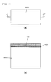
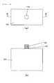
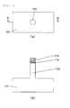
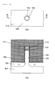
- the figure suffixed by (a) is a top plan view
- the figure suffixed by (b) is a sectional view taken along the line A-A'.
- a pad oxide film 112 is formed on a silicon substrate 101 to serve as a pad for reducing a stress between the silicon substrate and an after-mentioned hard mask. Subsequently, a silicon nitride film 110 is formed on the pad oxide film 112 to serve as a hard mask.
- a resist is patterned by lithography using a mask for a pillar-shaped silicon layer, and the pad oxide film 112 and the hard mask 110 are patterned by dry etching.
- the silicon substrate 101 is etched using the hard mask 110 to form a pillar-shaped silicon layer 102.
- an N+ diffusion layer 103 is formed in a diffusion region beneath the pillar-shaped silicon layer 102, by means of ion implantation or the like.
- a gate dielectric film 105 is formed.
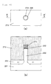
- a first gate conductive film 106 made of polysilicon is formed to allow the pillar-shaped silicon layer 102 to be buried therein.
- respective portions of the first gate conductive film 106 and the gate dielectric film 105 above the pillar-shaped silicon layer 102 are polished by chemical mechanical polishing (CMP), to flatten a top surface of the first gate conductive film 106.
- CMP chemical mechanical polishing
- the flattening of a top of the gate conductive film 106 by CMP facilitates control of a gate length, as described later.
- the hard mask 110 on top of the pillar-shaped silicon layer is used as a CMP stopper.
- a silicon nitride film may be used as the hard mask, as in the first embodiment. In this case, a selectivity ratio between the hard mask and the gate conductive film can be set to a large value to control a CMP amount with high repeatability.
- a second gate conductive film 111 made of polysilicon is formed.
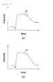
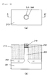
- FIG. 9(b) shows a structure at a timing when an etching end-point is detected after the hard mask is exposed.
- the plasma emission intensity sharply increases just after initiation of the etching (point A1).
- an amount of polysilicon to be etched decreases.
- the plasma emission intensity starts decreasing (point B1).
- An etching end-point can be detected by monitoring the above decrease in the plasma emission intensity.
- a film thickness of the second gate conductive film to be etched before the exposure of the hard mask depends on an amount of the second gate conductive film to be formed.
- an etching rate of the second gate conductive film 111 can be calculated based on the film thickness of the second gate conductive and a time taken from initiation to completion of the etching.
- the top of the first conductive film 106 flattened by polishing in advance as described above makes it possible to accurately determine an etched amount and an etching time of the second gate conductive film so as to accurately calculate an etching rate of the second gate conductive film.
- This etching rate can be used to calculate an overetching amount for a desired film thickness in consideration of an etching rate during etching of the first gate conductive film, so that a gate length can be set in a stable manner.
- an etching rate for actually etching the first gate conductive film can be calculated, based on an etching rate of the second gate conductive film calculated during actual etching of the second gate conductive film, and a relative ratio between respective etching rates of the first and second gate conductive films. Then, an etching time required for allowing the first gate conductive film to have a desired film thickness can be accurately obtained based on the above etching rate of the first gate conductive film.
- the hard mask 110 on top of the pillar-shaped silicon layer also has a function of protecting the pillar-shaped silicon layer from being etched during the above etching.
- each of the first gate conductive film and the second gate conductive film is made of polysilicon.
- the first gate conductive film and the second gate conductive film may be made of the same metal material.
- the first gate conductive film and the second gate conductive film may be made of the different metal material.
- an intensity of plasma emission from the second gate conductive film has a characteristic curve as shown in FIG. 10(b) . Specifically, the plasma emission intensity sharply increases just after initiation of the etching (point A2). Then, when the hard mask is exposed, the second gate conductive film is fully etched away. Thus, the plasma emission intensity starts decreasing (point B2).
- An etching end-point can be detected by monitoring the above decrease in the plasma emission intensity. Regardless of whether the first gate conductive film and the second gate conductive film are made of the same material or made of different materials, respectively, an etching amount of the first gate conductive film can be controlled in the same manner, as long as a relative ratio between respective etching rates of the first and second gate conductive films can be found out.
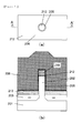
- an etching time of the first gate conductive film is determined based on an accurate etching rate of the first gate conductive film.
- the gate conductive film is formed to have a desired gate length for a gate electrode, as shown in FIGS. 11 (a) and 11(b) .
- the pad oxide film 112 and the hard mask 110 is removed by dry etching or wet etching. Subsequently, the gate conductive film is patterned to form a gate electrode 106a surrounding the pillar-shaped silicon layer, and a gate line 106b on which a contact is to be formed.
- an N+ source diffusion layer 104 is formed in an upper portion of the pillar-shaped silicon layer, by means of ion implantation or the like.
- an interlayer film is formed, and a contact (107, 108, 109) is formed.
- a contact 107, 108, 109 is formed.
- an SGT is formed.
- An SGT production method provides a technique of, during dry etching for forming a silicon oxide film to have a desired thickness for reducing a gate capacitance in such a manner as to be interposed between a gate electrode and a portion of a substrate beneath a pillar-shaped silicon layer, accurately controlling an etching amount of the silicon oxide film, using an end-point detection process based on monitoring a plasma emission intensity.
- FIG. 15(a) is a top plan view showing an NMOS SGT produced by the method according to the second embodiment
- FIG. 15(b) is a sectional view taken along the line A-A' in FIG. 15(a) .
- a pillar-shaped silicon layer 202 is formed on a silicon substrate 201, and a gate dielectric film 205 and a gate electrode 206a are formed around the pillar-shaped silicon layer 202.
- An N + drain diffusion layer 203 is formed beneath the pillar-shaped silicon layer 202, and an N + source diffusion layer 204 is formed on a top of the pillar-shaped silicon layer 202.
- a silicon oxide film 213 is formed between the N + drain diffusion layer 203 and the gate electrode 206a to reduce a gate capacitance.
- a contact 207, a contact 208, and a contact 209, are formed on the N + drain diffusion layer 203, the N + source diffusion layer 204, and a gate line 206b extending from the gate electrode 206a, respectively.
- the silicon oxide film 213 has a small film thickness of several tens of nm. Thus, it is necessary to accurately control the film thickness.
- a voltage ranging from zero to Vcc is applied to the gate electrode 206a to allow the SGT to operate as a transistor.
- FIGS. 16(a) to 21(b) show one example of the SGT production method.
- the figure suffixed by (a) is a top plan view
- the figure suffixed by (b) is a sectional view taken along the line A-A'.
- the step of forming an N + drain diffusion layer (see FIGS. 5(a) and 5(b) ) and any step therebefore are the same as those in the first embodiment. Thus, the following description will be made about steps subsequent to the N + drain diffusion layer forming step.
- a silicon oxide film 213 is formed to allow a pillar-shaped silicon layer 202 to be buried therein.
- a portion of the silicon oxide film 213 above the pillar-shaped silicon layer are polished by CMP, to flatten a top surface of the silicon oxide film.
- a hard mask 210 on top of the pillar-shaped silicon layer is used as a CMP stopper.
- a silicon nitride film may be used as the hard mask.
- a selectivity ratio between the hard mask and the silicon oxide film can be set to a large value to control a CMP amount with high repeatability.
- a silicon oxide film 213 is formed to allow the pillar-shaped silicon layer 202 to be buried therein.
- FIGS. 19(a) and 19(b) the silicon oxide film is etched back.
- FIG. 19(b) shows a structure at a timing when an etching end-point is detected after the silicon nitride film serving as the hard mask is exposed.
- An algorism for use in the end-point detection is the same as that (see FIG. 10(a) ) in the first embodiment.
- an etching rate of the silicon oxide film 213 is calculated, and an etching time required for allowing the silicon oxide film to have a desired film thickness is determined based on the calculated etching rate, in the same manner as that in the first embodiment.
- the silicon oxide film 213 is formed on the N+ drain diffusion layer 203 to have a desired film thickness for reducing a gate capacitance, as shown in FIGS. 20(a) and 20(b) .
- a gate dielectric film 205 and a gate conductive film 206 are formed. Subsequent steps are the same as those in the first embodiment, and their description will be omitted here.
- the present invention is not limited to the above embodiments, but encompasses any other SGT production method which comprises the steps of: forming a first dielectric or gate conductive film to allow a pillar-shaped semiconductor layer to be buried therein; flattening the first dielectric or gate conductive film while detecting an end-point using a stopper formed on top of the pillar-shaped semiconductor layer; forming a second dielectric or gate conductive film; etching the second dielectric or gate conductive film and calculating an etching rate during the etching; and detecting an end-point of etching of the first dielectric or gate conductive film, based on the etching rate of the second dielectric or gate conductive film during etching-back of the second dielectric or gate conductive film, to control an etching amount of the first dielectric or gate conductive film.
- the SGT production method of the present invention is capable of, during dry etching for forming a gate electrode, controlling an etching amount using an end-point detection process, to stably set a gate length and a substantial height dimension of a pillar-shaped silicon layer. This makes it possible to produce an SGT with stable characteristics.
Landscapes
- Insulated Gate Type Field-Effect Transistor (AREA)
- Drying Of Semiconductors (AREA)
- Electrodes Of Semiconductors (AREA)
Applications Claiming Priority (1)
| Application Number | Priority Date | Filing Date | Title |
|---|---|---|---|
| PCT/JP2008/065718 WO2010026620A1 (ja) | 2008-09-02 | 2008-09-02 | 半導体の製造方法 |
Publications (3)
| Publication Number | Publication Date |
|---|---|
| EP2159833A2 true EP2159833A2 (de) | 2010-03-03 |
| EP2159833A3 EP2159833A3 (de) | 2010-06-09 |
| EP2159833B1 EP2159833B1 (de) | 2015-04-29 |
Family
ID=41376396
Family Applications (1)
| Application Number | Title | Priority Date | Filing Date |
|---|---|---|---|
| EP20090169108 Active EP2159833B1 (de) | 2008-09-02 | 2009-09-01 | Verfahren zur Herstellung einer Halbleitervorrichtung |
Country Status (6)
| Country | Link |
|---|---|
| EP (1) | EP2159833B1 (de) |
| KR (1) | KR101255411B1 (de) |
| CN (1) | CN101667558B (de) |
| SG (1) | SG159460A1 (de) |
| TW (1) | TW201011864A (de) |
| WO (1) | WO2010026620A1 (de) |
Families Citing this family (2)
| Publication number | Priority date | Publication date | Assignee | Title |
|---|---|---|---|---|
| CN102479732B (zh) * | 2010-11-30 | 2013-12-25 | 中国科学院微电子研究所 | 监控栅槽刻蚀的方法 |
| CN112331615B (zh) * | 2021-01-06 | 2021-04-02 | 晶芯成(北京)科技有限公司 | 半导体器件的形成方法 |
Citations (1)
| Publication number | Priority date | Publication date | Assignee | Title |
|---|---|---|---|---|
| JPH02188966A (ja) | 1989-01-17 | 1990-07-25 | Toshiba Corp | Mos型半導体装置 |
Family Cites Families (7)
| Publication number | Priority date | Publication date | Assignee | Title |
|---|---|---|---|---|
| JP3230846B2 (ja) * | 1992-07-30 | 2001-11-19 | 株式会社東芝 | 半導体装置および半導体集積回路装置 |
| KR100475459B1 (ko) | 1998-02-11 | 2005-05-27 | 삼성전자주식회사 | 반도체 건식식각공정의 이피디용 파장 결정방법 및 이를 이용한이피디방법 |
| US6281068B1 (en) * | 1998-04-30 | 2001-08-28 | International Business Machines Corporation | Method for buried plate formation in deep trench capacitors |
| KR100473857B1 (ko) * | 2002-06-12 | 2005-03-10 | (주)쎄미시스코 | 반도체 건식 식각공정에서의 식각 종료점 검출방법 |
| JP2004128094A (ja) * | 2002-09-30 | 2004-04-22 | Toshiba Corp | 半導体装置の製造方法及び半導体製造システム |
| JP2004296491A (ja) * | 2003-03-25 | 2004-10-21 | Sanyo Electric Co Ltd | 半導体装置 |
| JP2006310651A (ja) * | 2005-04-28 | 2006-11-09 | Toshiba Corp | 半導体装置の製造方法 |
-
2008
- 2008-09-02 WO PCT/JP2008/065718 patent/WO2010026620A1/ja not_active Ceased
-
2009
- 2009-08-11 SG SG200905346-3A patent/SG159460A1/en unknown
- 2009-08-28 TW TW098128961A patent/TW201011864A/zh unknown
- 2009-09-01 EP EP20090169108 patent/EP2159833B1/de active Active
- 2009-09-01 KR KR1020090082204A patent/KR101255411B1/ko not_active Expired - Fee Related
- 2009-09-02 CN CN200910167294.6A patent/CN101667558B/zh active Active
Patent Citations (1)
| Publication number | Priority date | Publication date | Assignee | Title |
|---|---|---|---|---|
| JPH02188966A (ja) | 1989-01-17 | 1990-07-25 | Toshiba Corp | Mos型半導体装置 |
Non-Patent Citations (1)
| Title |
|---|
| RUIGANG LI ET AL.: "50 nm Vertical Surround Gate MOSFET with S-Factor of 75 mV/dec", DEVICE RESEARCH CONFERENCE, 2001, pages 63 |
Also Published As
| Publication number | Publication date |
|---|---|
| KR101255411B1 (ko) | 2013-04-17 |
| CN101667558A (zh) | 2010-03-10 |
| EP2159833B1 (de) | 2015-04-29 |
| EP2159833A3 (de) | 2010-06-09 |
| WO2010026620A1 (ja) | 2010-03-11 |
| CN101667558B (zh) | 2014-03-12 |
| SG159460A1 (en) | 2010-03-30 |
| KR20100027990A (ko) | 2010-03-11 |
| TW201011864A (en) | 2010-03-16 |
Similar Documents
| Publication | Publication Date | Title |
|---|---|---|
| US8211809B2 (en) | Method of producing semiconductor device | |
| TWI524397B (zh) | 具有改善的閾値電壓表現的取代金屬閘極的積體電路及其製造方法 | |
| US7754593B2 (en) | Semiconductor device and manufacturing method therefor | |
| US10084040B2 (en) | Seamless gap fill | |
| US20150024584A1 (en) | Methods for forming integrated circuits with reduced replacement metal gate height variability | |
| CN105977282A (zh) | 用于制造生物传感器的微阱的方法 | |
| CN103021867B (zh) | 沟槽型金属-氧化物-半导体势垒肖特基器件的形成方法 | |
| JPH07263677A (ja) | 半導体装置およびその製造方法 | |
| US8026141B2 (en) | Method of producing semiconductor | |
| US10014385B2 (en) | Manufacturing method of semiconductor device and semiconductor device | |
| EP2159833A2 (de) | Verfahren zur Herstellung einer Halbleitervorrichtung | |
| US9054025B2 (en) | Process for controlling shallow trench isolation step height | |
| EP2242108A1 (de) | Verfahren zur herstellung eines halbleiters | |
| CN100468679C (zh) | 半导体器件及半导体器件的制造方法和评估方法 | |
| JP2010098157A (ja) | 半導体装置の製造方法 | |
| JP2008072032A (ja) | 半導体装置の製造方法 | |
| US8530247B2 (en) | Control of implant pattern critical dimensions using STI step height offset | |
| JP4735876B2 (ja) | 半導体装置の製造方法 | |
| JP2010062565A6 (ja) | 半導体装置の製造方法 | |
| JP5258121B2 (ja) | 半導体の製造方法 | |
| US12471356B2 (en) | Stepped isolation regions | |
| JP2002252349A (ja) | パターンの形成方法 | |
| US20050067658A1 (en) | Dry etching method for semiconductor device | |
| US20080242023A1 (en) | Method for preparing a metal-oxide-semiconductor transistor | |
| US20160064293A1 (en) | Semiconductor arrangement and formation thereof |
Legal Events
| Date | Code | Title | Description |
|---|---|---|---|
| PUAI | Public reference made under article 153(3) epc to a published international application that has entered the european phase |
Free format text: ORIGINAL CODE: 0009012 |
|
| AK | Designated contracting states |
Kind code of ref document: A2 Designated state(s): AT BE BG CH CY CZ DE DK EE ES FI FR GB GR HR HU IE IS IT LI LT LU LV MC MK MT NL NO PL PT RO SE SI SK SM TR |
|
| PUAL | Search report despatched |
Free format text: ORIGINAL CODE: 0009013 |
|
| AK | Designated contracting states |
Kind code of ref document: A3 Designated state(s): AT BE BG CH CY CZ DE DK EE ES FI FR GB GR HR HU IE IS IT LI LT LU LV MC MK MT NL NO PL PT RO SE SI SK SM TR |
|
| 17P | Request for examination filed |
Effective date: 20101209 |
|
| RAP1 | Party data changed (applicant data changed or rights of an application transferred) |
Owner name: UNISANTIS ELECTRONICS SINGAPORE PTE. LTD. |
|
| RAP1 | Party data changed (applicant data changed or rights of an application transferred) |
Owner name: UNISANTIS ELECTRONICS SINGAPORE PTE. LTD. |
|
| 17Q | First examination report despatched |
Effective date: 20130328 |
|
| RIN1 | Information on inventor provided before grant (corrected) |
Inventor name: ARAI, SHINTARO Inventor name: MASUOKA, FUJIO |
|
| GRAP | Despatch of communication of intention to grant a patent |
Free format text: ORIGINAL CODE: EPIDOSNIGR1 |
|
| RIC1 | Information provided on ipc code assigned before grant |
Ipc: H01L 21/336 20060101AFI20150113BHEP Ipc: H01L 29/78 20060101ALI20150113BHEP Ipc: H01L 21/8238 20060101ALN20150113BHEP Ipc: H01L 21/66 20060101ALI20150113BHEP |
|
| INTG | Intention to grant announced |
Effective date: 20150202 |
|
| GRAS | Grant fee paid |
Free format text: ORIGINAL CODE: EPIDOSNIGR3 |
|
| GRAA | (expected) grant |
Free format text: ORIGINAL CODE: 0009210 |
|
| AK | Designated contracting states |
Kind code of ref document: B1 Designated state(s): AT BE BG CH CY CZ DE DK EE ES FI FR GB GR HR HU IE IS IT LI LT LU LV MC MK MT NL NO PL PT RO SE SI SK SM TR |
|
| REG | Reference to a national code |
Ref country code: GB Ref legal event code: FG4D |
|
| REG | Reference to a national code |
Ref country code: CH Ref legal event code: EP |
|
| REG | Reference to a national code |
Ref country code: AT Ref legal event code: REF Ref document number: 724855 Country of ref document: AT Kind code of ref document: T Effective date: 20150515 |
|
| REG | Reference to a national code |
Ref country code: IE Ref legal event code: FG4D |
|
| REG | Reference to a national code |
Ref country code: DE Ref legal event code: R096 Ref document number: 602009030925 Country of ref document: DE Effective date: 20150611 |
|
| REG | Reference to a national code |
Ref country code: DE Ref legal event code: R082 Ref document number: 602009030925 Country of ref document: DE Representative=s name: KINDERMANN, PETER, DIPL.-ING.UNIV., DE |
|
| REG | Reference to a national code |
Ref country code: NL Ref legal event code: VDEP Effective date: 20150429 |
|
| REG | Reference to a national code |
Ref country code: AT Ref legal event code: MK05 Ref document number: 724855 Country of ref document: AT Kind code of ref document: T Effective date: 20150429 |
|
| REG | Reference to a national code |
Ref country code: FR Ref legal event code: PLFP Year of fee payment: 7 |
|
| REG | Reference to a national code |
Ref country code: LT Ref legal event code: MG4D |
|
| PG25 | Lapsed in a contracting state [announced via postgrant information from national office to epo] |
Ref country code: NL Free format text: LAPSE BECAUSE OF FAILURE TO SUBMIT A TRANSLATION OF THE DESCRIPTION OR TO PAY THE FEE WITHIN THE PRESCRIBED TIME-LIMIT Effective date: 20150429 |
|
| PG25 | Lapsed in a contracting state [announced via postgrant information from national office to epo] |
Ref country code: HR Free format text: LAPSE BECAUSE OF FAILURE TO SUBMIT A TRANSLATION OF THE DESCRIPTION OR TO PAY THE FEE WITHIN THE PRESCRIBED TIME-LIMIT Effective date: 20150429 Ref country code: NO Free format text: LAPSE BECAUSE OF FAILURE TO SUBMIT A TRANSLATION OF THE DESCRIPTION OR TO PAY THE FEE WITHIN THE PRESCRIBED TIME-LIMIT Effective date: 20150729 Ref country code: PT Free format text: LAPSE BECAUSE OF FAILURE TO SUBMIT A TRANSLATION OF THE DESCRIPTION OR TO PAY THE FEE WITHIN THE PRESCRIBED TIME-LIMIT Effective date: 20150831 Ref country code: FI Free format text: LAPSE BECAUSE OF FAILURE TO SUBMIT A TRANSLATION OF THE DESCRIPTION OR TO PAY THE FEE WITHIN THE PRESCRIBED TIME-LIMIT Effective date: 20150429 Ref country code: ES Free format text: LAPSE BECAUSE OF FAILURE TO SUBMIT A TRANSLATION OF THE DESCRIPTION OR TO PAY THE FEE WITHIN THE PRESCRIBED TIME-LIMIT Effective date: 20150429 Ref country code: LT Free format text: LAPSE BECAUSE OF FAILURE TO SUBMIT A TRANSLATION OF THE DESCRIPTION OR TO PAY THE FEE WITHIN THE PRESCRIBED TIME-LIMIT Effective date: 20150429 |
|
| PG25 | Lapsed in a contracting state [announced via postgrant information from national office to epo] |
Ref country code: LV Free format text: LAPSE BECAUSE OF FAILURE TO SUBMIT A TRANSLATION OF THE DESCRIPTION OR TO PAY THE FEE WITHIN THE PRESCRIBED TIME-LIMIT Effective date: 20150429 Ref country code: AT Free format text: LAPSE BECAUSE OF FAILURE TO SUBMIT A TRANSLATION OF THE DESCRIPTION OR TO PAY THE FEE WITHIN THE PRESCRIBED TIME-LIMIT Effective date: 20150429 Ref country code: IS Free format text: LAPSE BECAUSE OF FAILURE TO SUBMIT A TRANSLATION OF THE DESCRIPTION OR TO PAY THE FEE WITHIN THE PRESCRIBED TIME-LIMIT Effective date: 20150829 Ref country code: GR Free format text: LAPSE BECAUSE OF FAILURE TO SUBMIT A TRANSLATION OF THE DESCRIPTION OR TO PAY THE FEE WITHIN THE PRESCRIBED TIME-LIMIT Effective date: 20150730 |
|
| PG25 | Lapsed in a contracting state [announced via postgrant information from national office to epo] |
Ref country code: EE Free format text: LAPSE BECAUSE OF FAILURE TO SUBMIT A TRANSLATION OF THE DESCRIPTION OR TO PAY THE FEE WITHIN THE PRESCRIBED TIME-LIMIT Effective date: 20150429 Ref country code: DK Free format text: LAPSE BECAUSE OF FAILURE TO SUBMIT A TRANSLATION OF THE DESCRIPTION OR TO PAY THE FEE WITHIN THE PRESCRIBED TIME-LIMIT Effective date: 20150429 |
|
| REG | Reference to a national code |
Ref country code: DE Ref legal event code: R097 Ref document number: 602009030925 Country of ref document: DE |
|
| PG25 | Lapsed in a contracting state [announced via postgrant information from national office to epo] |
Ref country code: RO Free format text: LAPSE BECAUSE OF NON-PAYMENT OF DUE FEES Effective date: 20150429 Ref country code: SK Free format text: LAPSE BECAUSE OF FAILURE TO SUBMIT A TRANSLATION OF THE DESCRIPTION OR TO PAY THE FEE WITHIN THE PRESCRIBED TIME-LIMIT Effective date: 20150429 Ref country code: CZ Free format text: LAPSE BECAUSE OF FAILURE TO SUBMIT A TRANSLATION OF THE DESCRIPTION OR TO PAY THE FEE WITHIN THE PRESCRIBED TIME-LIMIT Effective date: 20150429 Ref country code: PL Free format text: LAPSE BECAUSE OF FAILURE TO SUBMIT A TRANSLATION OF THE DESCRIPTION OR TO PAY THE FEE WITHIN THE PRESCRIBED TIME-LIMIT Effective date: 20150429 |
|
| PLBE | No opposition filed within time limit |
Free format text: ORIGINAL CODE: 0009261 |
|
| STAA | Information on the status of an ep patent application or granted ep patent |
Free format text: STATUS: NO OPPOSITION FILED WITHIN TIME LIMIT |
|
| 26N | No opposition filed |
Effective date: 20160201 |
|
| PG25 | Lapsed in a contracting state [announced via postgrant information from national office to epo] |
Ref country code: LU Free format text: LAPSE BECAUSE OF FAILURE TO SUBMIT A TRANSLATION OF THE DESCRIPTION OR TO PAY THE FEE WITHIN THE PRESCRIBED TIME-LIMIT Effective date: 20150901 Ref country code: MC Free format text: LAPSE BECAUSE OF FAILURE TO SUBMIT A TRANSLATION OF THE DESCRIPTION OR TO PAY THE FEE WITHIN THE PRESCRIBED TIME-LIMIT Effective date: 20150429 |
|
| REG | Reference to a national code |
Ref country code: CH Ref legal event code: PL |
|
| PG25 | Lapsed in a contracting state [announced via postgrant information from national office to epo] |
Ref country code: SI Free format text: LAPSE BECAUSE OF FAILURE TO SUBMIT A TRANSLATION OF THE DESCRIPTION OR TO PAY THE FEE WITHIN THE PRESCRIBED TIME-LIMIT Effective date: 20150429 |
|
| REG | Reference to a national code |
Ref country code: IE Ref legal event code: MM4A |
|
| PG25 | Lapsed in a contracting state [announced via postgrant information from national office to epo] |
Ref country code: LI Free format text: LAPSE BECAUSE OF NON-PAYMENT OF DUE FEES Effective date: 20150930 Ref country code: CH Free format text: LAPSE BECAUSE OF NON-PAYMENT OF DUE FEES Effective date: 20150930 Ref country code: IE Free format text: LAPSE BECAUSE OF NON-PAYMENT OF DUE FEES Effective date: 20150901 |
|
| PG25 | Lapsed in a contracting state [announced via postgrant information from national office to epo] |
Ref country code: BE Free format text: LAPSE BECAUSE OF FAILURE TO SUBMIT A TRANSLATION OF THE DESCRIPTION OR TO PAY THE FEE WITHIN THE PRESCRIBED TIME-LIMIT Effective date: 20150429 |
|
| REG | Reference to a national code |
Ref country code: FR Ref legal event code: PLFP Year of fee payment: 8 |
|
| PG25 | Lapsed in a contracting state [announced via postgrant information from national office to epo] |
Ref country code: MT Free format text: LAPSE BECAUSE OF FAILURE TO SUBMIT A TRANSLATION OF THE DESCRIPTION OR TO PAY THE FEE WITHIN THE PRESCRIBED TIME-LIMIT Effective date: 20150429 |
|
| PG25 | Lapsed in a contracting state [announced via postgrant information from national office to epo] |
Ref country code: SM Free format text: LAPSE BECAUSE OF FAILURE TO SUBMIT A TRANSLATION OF THE DESCRIPTION OR TO PAY THE FEE WITHIN THE PRESCRIBED TIME-LIMIT Effective date: 20150429 Ref country code: HU Free format text: LAPSE BECAUSE OF FAILURE TO SUBMIT A TRANSLATION OF THE DESCRIPTION OR TO PAY THE FEE WITHIN THE PRESCRIBED TIME-LIMIT; INVALID AB INITIO Effective date: 20090901 Ref country code: BG Free format text: LAPSE BECAUSE OF FAILURE TO SUBMIT A TRANSLATION OF THE DESCRIPTION OR TO PAY THE FEE WITHIN THE PRESCRIBED TIME-LIMIT Effective date: 20150429 |
|
| PG25 | Lapsed in a contracting state [announced via postgrant information from national office to epo] |
Ref country code: SE Free format text: LAPSE BECAUSE OF FAILURE TO SUBMIT A TRANSLATION OF THE DESCRIPTION OR TO PAY THE FEE WITHIN THE PRESCRIBED TIME-LIMIT Effective date: 20150429 Ref country code: CY Free format text: LAPSE BECAUSE OF FAILURE TO SUBMIT A TRANSLATION OF THE DESCRIPTION OR TO PAY THE FEE WITHIN THE PRESCRIBED TIME-LIMIT Effective date: 20150429 |
|
| PG25 | Lapsed in a contracting state [announced via postgrant information from national office to epo] |
Ref country code: TR Free format text: LAPSE BECAUSE OF FAILURE TO SUBMIT A TRANSLATION OF THE DESCRIPTION OR TO PAY THE FEE WITHIN THE PRESCRIBED TIME-LIMIT Effective date: 20150429 |
|
| REG | Reference to a national code |
Ref country code: FR Ref legal event code: PLFP Year of fee payment: 9 |
|
| PG25 | Lapsed in a contracting state [announced via postgrant information from national office to epo] |
Ref country code: MK Free format text: LAPSE BECAUSE OF FAILURE TO SUBMIT A TRANSLATION OF THE DESCRIPTION OR TO PAY THE FEE WITHIN THE PRESCRIBED TIME-LIMIT Effective date: 20150429 |
|
| REG | Reference to a national code |
Ref country code: FR Ref legal event code: PLFP Year of fee payment: 10 |
|
| REG | Reference to a national code |
Ref country code: DE Ref legal event code: R082 Ref document number: 602009030925 Country of ref document: DE Representative=s name: PAGE, WHITE & FARRER GERMANY LLP, DE Ref country code: DE Ref legal event code: R082 Ref document number: 602009030925 Country of ref document: DE Representative=s name: GULDE & PARTNER PATENT- UND RECHTSANWALTSKANZL, DE |
|
| REG | Reference to a national code |
Ref country code: DE Ref legal event code: R079 Ref document number: 602009030925 Country of ref document: DE Free format text: PREVIOUS MAIN CLASS: H01L0021336000 Ipc: H10D0030010000 |
|
| PGFP | Annual fee paid to national office [announced via postgrant information from national office to epo] |
Ref country code: DE Payment date: 20250919 Year of fee payment: 17 |
|
| PGFP | Annual fee paid to national office [announced via postgrant information from national office to epo] |
Ref country code: IT Payment date: 20250923 Year of fee payment: 17 |
|
| PGFP | Annual fee paid to national office [announced via postgrant information from national office to epo] |
Ref country code: GB Payment date: 20250918 Year of fee payment: 17 |
|
| PGFP | Annual fee paid to national office [announced via postgrant information from national office to epo] |
Ref country code: FR Payment date: 20250919 Year of fee payment: 17 |
|
| REG | Reference to a national code |
Ref country code: DE Ref legal event code: R082 Ref document number: 602009030925 Country of ref document: DE Representative=s name: GULDE & PARTNER PATENT- UND RECHTSANWALTSKANZL, DE |